WO1997049778A1 - Materiau absorbant les ultraviolets et plaques d'absorption des ultraviolets - Google Patents
Materiau absorbant les ultraviolets et plaques d'absorption des ultraviolets Download PDFInfo
- Publication number
- WO1997049778A1 WO1997049778A1 PCT/JP1997/002240 JP9702240W WO9749778A1 WO 1997049778 A1 WO1997049778 A1 WO 1997049778A1 JP 9702240 W JP9702240 W JP 9702240W WO 9749778 A1 WO9749778 A1 WO 9749778A1
- Authority
- WO
- WIPO (PCT)
- Prior art keywords
- ultraviolet
- group
- ultraviolet absorbing
- substrate
- carbon atoms
- Prior art date
- Legal status (The legal status is an assumption and is not a legal conclusion. Google has not performed a legal analysis and makes no representation as to the accuracy of the status listed.)
- Ceased
Links
Classifications
-
- C—CHEMISTRY; METALLURGY
- C03—GLASS; MINERAL OR SLAG WOOL
- C03C—CHEMICAL COMPOSITION OF GLASSES, GLAZES OR VITREOUS ENAMELS; SURFACE TREATMENT OF GLASS; SURFACE TREATMENT OF FIBRES OR FILAMENTS MADE FROM GLASS, MINERALS OR SLAGS; JOINING GLASS TO GLASS OR OTHER MATERIALS
- C03C17/00—Surface treatment of glass, not in the form of fibres or filaments, by coating
- C03C17/28—Surface treatment of glass, not in the form of fibres or filaments, by coating with organic material
- C03C17/30—Surface treatment of glass, not in the form of fibres or filaments, by coating with organic material with silicon-containing compounds
-
- C—CHEMISTRY; METALLURGY
- C09—DYES; PAINTS; POLISHES; NATURAL RESINS; ADHESIVES; COMPOSITIONS NOT OTHERWISE PROVIDED FOR; APPLICATIONS OF MATERIALS NOT OTHERWISE PROVIDED FOR
- C09K—MATERIALS FOR MISCELLANEOUS APPLICATIONS, NOT PROVIDED FOR ELSEWHERE
- C09K3/00—Materials not provided for elsewhere
-
- B—PERFORMING OPERATIONS; TRANSPORTING
- B32—LAYERED PRODUCTS
- B32B—LAYERED PRODUCTS, i.e. PRODUCTS BUILT-UP OF STRATA OF FLAT OR NON-FLAT, e.g. CELLULAR OR HONEYCOMB, FORM
- B32B17/00—Layered products essentially comprising sheet glass, or glass, slag, or like fibres
- B32B17/06—Layered products essentially comprising sheet glass, or glass, slag, or like fibres comprising glass as the main or only constituent of a layer, next to another layer of a specific material
- B32B17/10—Layered products essentially comprising sheet glass, or glass, slag, or like fibres comprising glass as the main or only constituent of a layer, next to another layer of a specific material of synthetic resin
- B32B17/10005—Layered products essentially comprising sheet glass, or glass, slag, or like fibres comprising glass as the main or only constituent of a layer, next to another layer of a specific material of synthetic resin laminated safety glass or glazing
-
- B—PERFORMING OPERATIONS; TRANSPORTING
- B32—LAYERED PRODUCTS
- B32B—LAYERED PRODUCTS, i.e. PRODUCTS BUILT-UP OF STRATA OF FLAT OR NON-FLAT, e.g. CELLULAR OR HONEYCOMB, FORM
- B32B17/00—Layered products essentially comprising sheet glass, or glass, slag, or like fibres
- B32B17/06—Layered products essentially comprising sheet glass, or glass, slag, or like fibres comprising glass as the main or only constituent of a layer, next to another layer of a specific material
- B32B17/10—Layered products essentially comprising sheet glass, or glass, slag, or like fibres comprising glass as the main or only constituent of a layer, next to another layer of a specific material of synthetic resin
- B32B17/10005—Layered products essentially comprising sheet glass, or glass, slag, or like fibres comprising glass as the main or only constituent of a layer, next to another layer of a specific material of synthetic resin laminated safety glass or glazing
- B32B17/10165—Functional features of the laminated safety glass or glazing
-
- C—CHEMISTRY; METALLURGY
- C08—ORGANIC MACROMOLECULAR COMPOUNDS; THEIR PREPARATION OR CHEMICAL WORKING-UP; COMPOSITIONS BASED THEREON
- C08G—MACROMOLECULAR COMPOUNDS OBTAINED OTHERWISE THAN BY REACTIONS ONLY INVOLVING UNSATURATED CARBON-TO-CARBON BONDS
- C08G77/00—Macromolecular compounds obtained by reactions forming a linkage containing silicon with or without sulfur, nitrogen, oxygen or carbon in the main chain of the macromolecule
- C08G77/04—Polysiloxanes
- C08G77/38—Polysiloxanes modified by chemical after-treatment
- C08G77/382—Polysiloxanes modified by chemical after-treatment containing atoms other than carbon, hydrogen, oxygen or silicon
- C08G77/388—Polysiloxanes modified by chemical after-treatment containing atoms other than carbon, hydrogen, oxygen or silicon containing nitrogen
-
- C—CHEMISTRY; METALLURGY
- C09—DYES; PAINTS; POLISHES; NATURAL RESINS; ADHESIVES; COMPOSITIONS NOT OTHERWISE PROVIDED FOR; APPLICATIONS OF MATERIALS NOT OTHERWISE PROVIDED FOR
- C09D—COATING COMPOSITIONS, e.g. PAINTS, VARNISHES OR LACQUERS; FILLING PASTES; CHEMICAL PAINT OR INK REMOVERS; INKS; CORRECTING FLUIDS; WOODSTAINS; PASTES OR SOLIDS FOR COLOURING OR PRINTING; USE OF MATERIALS THEREFOR
- C09D183/00—Coating compositions based on macromolecular compounds obtained by reactions forming in the main chain of the macromolecule a linkage containing silicon, with or without sulfur, nitrogen, oxygen, or carbon only; Coating compositions based on derivatives of such polymers
- C09D183/04—Polysiloxanes
- C09D183/08—Polysiloxanes containing silicon bound to organic groups containing atoms other than carbon, hydrogen, and oxygen
-
- G—PHYSICS
- G02—OPTICS
- G02F—OPTICAL DEVICES OR ARRANGEMENTS FOR THE CONTROL OF LIGHT BY MODIFICATION OF THE OPTICAL PROPERTIES OF THE MEDIA OF THE ELEMENTS INVOLVED THEREIN; NON-LINEAR OPTICS; FREQUENCY-CHANGING OF LIGHT; OPTICAL LOGIC ELEMENTS; OPTICAL ANALOGUE/DIGITAL CONVERTERS
- G02F1/00—Devices or arrangements for the control of the intensity, colour, phase, polarisation or direction of light arriving from an independent light source, e.g. switching, gating or modulating; Non-linear optics
- G02F1/01—Devices or arrangements for the control of the intensity, colour, phase, polarisation or direction of light arriving from an independent light source, e.g. switching, gating or modulating; Non-linear optics for the control of the intensity, phase, polarisation or colour
- G02F1/13—Devices or arrangements for the control of the intensity, colour, phase, polarisation or direction of light arriving from an independent light source, e.g. switching, gating or modulating; Non-linear optics for the control of the intensity, phase, polarisation or colour based on liquid crystals, e.g. single liquid crystal display cells
- G02F1/133—Constructional arrangements; Operation of liquid crystal cells; Circuit arrangements
- G02F1/1333—Constructional arrangements; Manufacturing methods
- G02F1/1335—Structural association of cells with optical devices, e.g. polarisers or reflectors
- G02F1/133509—Filters, e.g. light shielding masks
-
- Y—GENERAL TAGGING OF NEW TECHNOLOGICAL DEVELOPMENTS; GENERAL TAGGING OF CROSS-SECTIONAL TECHNOLOGIES SPANNING OVER SEVERAL SECTIONS OF THE IPC; TECHNICAL SUBJECTS COVERED BY FORMER USPC CROSS-REFERENCE ART COLLECTIONS [XRACs] AND DIGESTS
- Y10—TECHNICAL SUBJECTS COVERED BY FORMER USPC
- Y10T—TECHNICAL SUBJECTS COVERED BY FORMER US CLASSIFICATION
- Y10T428/00—Stock material or miscellaneous articles
- Y10T428/25—Web or sheet containing structurally defined element or component and including a second component containing structurally defined particles
- Y10T428/259—Silicic material
-
- Y—GENERAL TAGGING OF NEW TECHNOLOGICAL DEVELOPMENTS; GENERAL TAGGING OF CROSS-SECTIONAL TECHNOLOGIES SPANNING OVER SEVERAL SECTIONS OF THE IPC; TECHNICAL SUBJECTS COVERED BY FORMER USPC CROSS-REFERENCE ART COLLECTIONS [XRACs] AND DIGESTS
- Y10—TECHNICAL SUBJECTS COVERED BY FORMER USPC
- Y10T—TECHNICAL SUBJECTS COVERED BY FORMER US CLASSIFICATION
- Y10T428/00—Stock material or miscellaneous articles
- Y10T428/31504—Composite [nonstructural laminate]
- Y10T428/31551—Of polyamidoester [polyurethane, polyisocyanate, polycarbamate, etc.]
- Y10T428/31609—Particulate metal or metal compound-containing
- Y10T428/31612—As silicone, silane or siloxane
-
- Y—GENERAL TAGGING OF NEW TECHNOLOGICAL DEVELOPMENTS; GENERAL TAGGING OF CROSS-SECTIONAL TECHNOLOGIES SPANNING OVER SEVERAL SECTIONS OF THE IPC; TECHNICAL SUBJECTS COVERED BY FORMER USPC CROSS-REFERENCE ART COLLECTIONS [XRACs] AND DIGESTS
- Y10—TECHNICAL SUBJECTS COVERED BY FORMER USPC
- Y10T—TECHNICAL SUBJECTS COVERED BY FORMER US CLASSIFICATION
- Y10T428/00—Stock material or miscellaneous articles
- Y10T428/31504—Composite [nonstructural laminate]
- Y10T428/31652—Of asbestos
- Y10T428/31663—As siloxane, silicone or silane
-
- Y—GENERAL TAGGING OF NEW TECHNOLOGICAL DEVELOPMENTS; GENERAL TAGGING OF CROSS-SECTIONAL TECHNOLOGIES SPANNING OVER SEVERAL SECTIONS OF THE IPC; TECHNICAL SUBJECTS COVERED BY FORMER USPC CROSS-REFERENCE ART COLLECTIONS [XRACs] AND DIGESTS
- Y10—TECHNICAL SUBJECTS COVERED BY FORMER USPC
- Y10T—TECHNICAL SUBJECTS COVERED BY FORMER US CLASSIFICATION
- Y10T428/00—Stock material or miscellaneous articles
- Y10T428/31504—Composite [nonstructural laminate]
- Y10T428/31652—Of asbestos
- Y10T428/31667—Next to addition polymer from unsaturated monomers, or aldehyde or ketone condensation product
Definitions
- the present invention relates to an ultraviolet absorbing material and an ultraviolet absorbing plate.
- the method (1) of treating with an ultraviolet-absorbing substance includes an inorganic ultraviolet absorber and an organic ultraviolet absorber.
- Inorganic UV absorbers for example, JP-A-5-339033, JP-A-5-345569, JP-A-6-56466, etc.
- many long-wavelength kits are accompanied by coloring.
- organic UV absorbers have a wide absorption band, so that various types of absorption wavelengths can be obtained by selecting the type, concentration, and film thickness of the absorber.
- Systems using various organic UV absorbers have been studied so far, and when cutting to the long wavelength region, use one with a maximum absorption wavelength in the long wavelength region or increase the concentration or film thickness.
- those having a maximum absorption wavelength in a long wavelength region have poor light resistance, and the absorption capacity decreases with time.
- Japanese Patent Application Laid-Open No. Hei 6-145,887 there is also a problem that the use of a fluorescent whitening agent results in poor visibility due to fluorescence.
- Benzophenone and benzotriazole UV absorbers are compared The light resistance is good, and the concentration and film thickness can be increased to clear relatively long wavelengths.
- the concentration and film thickness can be increased to clear relatively long wavelengths.
- the film thickness is limited to about several tens of ⁇ m. In order to cut to a long wavelength region with this film thickness, it is necessary to add an ultraviolet absorber at a considerably high concentration. However, there is a problem in that simply adding it at a high concentration causes precipitation of the ultraviolet absorber and premature drop due to long-term use.
- one of the objects of the present invention is to realize a long-wavelength power that is easy to synthesize, does not cause bleed-out of an ultraviolet absorber even during long-term use, and contains a high concentration of an ultraviolet absorber.
- Another object of the present invention is to provide an ultraviolet absorbing material which does not cause any adverse effects even when the ultraviolet absorbing agent is excellent in weather resistance and heat resistance.
- An object of the present invention is to provide an ultraviolet absorbing plate capable of focusing on a long wavelength region of ultraviolet light without lowering the transmittance of the region. Disclosure of the invention
- the ultraviolet absorbing material of the present invention comprises: (a) an amino silane compound represented by the following general formula (1) or a derivative thereof;
- R 1 is an alkylene group having 1 to 10 carbon atoms, or a general formula — (CH 2 ) m -N H— [m is a divalent group represented by l ⁇ m ⁇ 4], and each R 2 is the same or different and represents a hydrogen atom, a hydroxyl group, a halogen atom, a carbon atom of 1 And represents an alkyl group having up to 10 or an alkoxy group having 1 to 10 carbon atoms. However, at least one of all R 2 represents an alkoxy group.
- n represents an integer of n ⁇ 0.
- the ultraviolet absorbing plate of the present invention is provided with an ultraviolet absorbing layer provided on a substrate to be processed, wherein the ultraviolet absorbing layer is formed of an ultraviolet absorbing material having an amide bond and a Si 10 bond. is there.
- the ultraviolet absorber comprises: (a) an aminosilane compound represented by the following general formula (1) or a derivative thereof;
- R 1 represents an alkylene group having 1 to 10 carbon atoms, or a divalent group represented by the general formula — (CH 2 ) m-NH— [m is an integer of l ⁇ m ⁇ 4]
- each R 2 is the same or different, and represents a hydrogen atom, a hydroxyl group, a halogen atom, an alkyl group having 1 to 10 carbon atoms, or an alkoxy group having 1 to 10 carbon atoms. At least one of 2 represents an alkoxy group, and n represents an integer of n ⁇ 0.
- reaction between the above-mentioned amino silane compound or its derivative and an ultraviolet absorber having a carboxyl group in the molecule is carried out in the presence of a silicone resin, or silicon is added after the reaction. Is preferred.
- the ultraviolet absorber comprises: (a) an amino silane compound represented by the following general formula (1) or a derivative thereof;
- R 1 represents an alkylene group having 1 or more carbon atoms: L 0, or a divalent group represented by the general formula — (CH 2 ) m -NH— [m is an integer of l ⁇ m ⁇ 4]
- each R 2 is the same or different and represents a hydrogen atom, a hydroxyl group, a halogen atom, an alkyl group having 1 to 10 carbon atoms, or an alkoxy group having 1 to 10 carbon atoms. At least one of R 2 represents an alkoxy group, and n represents an integer of n ⁇ 0.
- the substrate to be processed is formed by laminating a plurality of transparent substrates, and the ultraviolet absorbing layer is provided at least at one position between the transparent substrates.
- a transparent conductive film is provided on the substrate to be processed on the ultraviolet absorption layer side. It is preferable to have an overcoat layer between the ultraviolet absorbing layer and the transparent conductive film.
- FIG. 1 is a schematic sectional view showing an example of the ultraviolet absorbing plate of the present invention.
- FIG. 2 is a schematic sectional view showing another example of the ultraviolet absorbing plate of the present invention.
- FIG. 3 is a schematic sectional view showing another example of the ultraviolet absorbing plate of the present invention.
- FIG. 4 is a schematic sectional view showing another example of the ultraviolet absorbing plate of the present invention.
- FIG. 5 is a graph showing an ultraviolet-visible absorption spectrum of the ultraviolet absorbing glass prepared in Example 1.
- FIG. 6 is a graph showing an ultraviolet-visible absorption spectrum of the ultraviolet absorbing glass prepared in Example 9.
- FIG. 7 is a graph showing an ultraviolet-visible absorption spectrum of the ultraviolet absorbing glass prepared in Example 13;
- FIG. 8 is a graph showing an ultraviolet-visible absorption spectrum of the ultraviolet absorbing glass prepared in Example 17.
- FIG. 9 is a graph showing an ultraviolet-visible absorption spectrum of the ultraviolet absorbing glass prepared in Example 21.
- FIG. 10 is a graph showing an ultraviolet-visible absorption spectrum of the ultraviolet absorbing glass prepared in Example 25.
- FIG. 11 is a graph showing an ultraviolet-visible absorption spectrum of the ultraviolet absorbing glass prepared in Comparative Example 3.
- FIG. 12 is a graph for explaining, in a model, the principle of how to determine the rate of change in ultraviolet absorption capacity.
- the substrate to be processed in the present invention may be a transparent substrate or an opaque substrate, or may be a plurality of laminated substrates.
- the transparent substrate is not particularly limited, but, for example, colorless or colored glass, clear glass, meshed glass, heat-reflecting glass, heat-absorbing glass, tempered glass, glass block, or the like, or colorless or colored Transparent resin may be used.
- Transparent resins include polyethylene terephthalate, polyamide, polysulfone, polyether sulfone, polyether ketone, polyphenylene sulfide, polycarbonate, polyimide, and polymethyl methacrylate. And polystyrene.
- Transparent in the present invention means having a visible light transmittance of 3 to 100%, preferably 10 to 100%.
- the substrate in the present invention means a smooth surface at room temperature. The surface may be flat or curved, may be deformed by stress, or may be a container.
- the material of the opaque substrate is not particularly limited, and includes, for example, various types of glass such as soda-lime glass and borate glass, synthetic resin, paper, wood, woven fabric, nonwoven fabric, knitted fabric, and a combination of two or more thereof.
- the composite material used can be used.
- the above synthetic resins include polyethylene terephthalate, polyamide, polysulfone, polyethersulfone, polyphenylene sulfide, polycarbonate, polyimide, polymethylmethacrylate, polystyrene, etc. Is mentioned.
- the opaque substrate can be white or colored.
- the term "opaque” in the present invention refers to substantially impervious to visible light, and the opaque substrate of the present invention generally has a light transmittance of less than 3%, preferably less than 2% at a thickness of 2 / m.
- the opaque substrate used in the present invention usually has a so-called surface macroscopically, but the surface does not need to be microscopically smooth. Also, the surface of the opaque substrate may be flat or curved, and the surface may be deformed by external force. It is essential that the ultraviolet absorbing layer in the present invention has an amide bond (—CONH—) and a Si—0 bond. Preferably, it is desirable to have a structure in which the amide bond and the Si 10 bond are further bonded by some kind of bonding group.
- linking group for example,
- the content of the amide bond and the Si—0 bond in the ultraviolet absorbing layer is such that 1-10 bonds per mole of the amide bond is usually 1 to 50 mol, preferably 1 to 3 mol. 0 mol, more preferably in the range of 1 to 15 mol is desirable.
- a preferred embodiment of the ultraviolet absorbing plate of the present invention includes a transparent substrate and an ultraviolet absorbing layer.
- a transparent ultraviolet-absorbing transparent plate is extracted with boiling acetone for 24 hours, the following equation (1) is obtained.
- the absorbance change before the extraction is calculated using the absorbance at any one wavelength in the ultraviolet region when the absorbance is substantially 1.
- the change in the ultraviolet absorption ability can be easily confirmed by the ultraviolet absorption spectrum.
- Fig. 12 shows a model of the principle of how to determine the rate of change in ultraviolet absorptivity.
- the wavelength at an absorbance of 1 before extraction is about 383 nm.
- the absorbance at the wavelength after extraction is about 0.07. Therefore, the rate of change in ultraviolet absorption capacity in this case is found to be 93%.
- the rate of change in ultraviolet absorption capacity usually occurs because components derived from the ultraviolet absorbing compound (usually an organic ultraviolet absorbing compound) used for forming the ultraviolet absorbing layer are eluted into acetone.
- the ultraviolet absorbing component forms a chemical bond with other members in the ultraviolet absorbing layer, the ultraviolet absorbing component is not substantially eluted.
- benzotriazole is used as an ultraviolet absorbing compound.
- an organic ultraviolet absorber having a skeleton or a benzofunone skeleton (described later)
- the resulting ultraviolet absorbing layer usually has a benzotriazole skeleton, a benzophenone skeleton or a structure derived therefrom.
- the ultraviolet absorbing compound in the ultraviolet absorbing layer is bonded to the base material through an amide bond, Even if the ultraviolet absorbing layer is boiled in acetone, the structure derived from the ultraviolet absorbing agent is not extracted, or the amount of the extraction is extremely small. The amount of change can be small.
- the method for producing such a specific ultraviolet absorbing layer is not particularly limited, and can be obtained by any method. Suitable methods include the following methods. That is, (a) an aminosilane compound or its derivative represented by the following general formula (1) (hereinafter, referred to as “component A”); and (b) an ultraviolet absorber having a carboxyl group in the molecule (hereinafter, referred to as “component A”). This is referred to as “component B.) A method in which an amide bond derived from a substance or a derivative thereof is reacted to generate an ultraviolet absorber, and the ultraviolet absorber is applied on a transparent substrate or the like and cured.
- component A an aminosilane compound or its derivative represented by the following general formula (1)
- component A an ultraviolet absorber having a carboxyl group in the molecule
- R 2 R 2 ⁇ ! Is an alkylene group having 1 to 5 carbon atoms, preferably 1 to 5 or a divalent group represented by the general formula — (CH 2 ) m-NH- (m is an integer of l ⁇ m ⁇ 4) Show.
- Examples of the alkylene group for R 1 include a methylene group, an ethylene group, a trimethylene group, a propylene group and the like.
- each of R 2 may be the same Wakashi Ku different groups, a hydrogen atom, a hydroxyl group, a carbon number 1 to 1 0, favored properly 1-3 alkyl group, having 1 to 1 0 carbon atoms, the preferred properly It represents an alkoxy group having 1 to 5 or a aryl group having 6 to 10 carbon atoms, preferably 6 to 8 carbon atoms. At least one of all R 2 is preferably an alkoxy group having 1 to 5 carbon atoms.
- n represents an integer n ⁇ 0, preferably 0 ⁇ n ⁇ 3.
- the amino silane compound represented by the general formula (1) is preferably 3-amino propyl ethoxy silane, 3-amino propyl diisopropyl ethoxy silane, 3-amino propyl methyl ethoxy silane. , 3-aminopropylpolydimethylsiloxane, N- (2-aminoethyl) -13-aminopropyltrimethoxysilane, 3-aminopropyltris (methoxhetoxy) silane, etc. And hydrolysates thereof can be preferably cited as derivatives of the aminosilane compound.
- These aminosilane compounds or derivatives thereof can be produced by a known method.
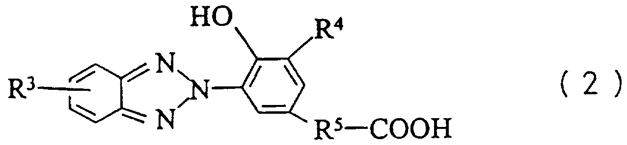
- the ultraviolet absorber having a carboxyl group in the molecule as the component B include a compound having one or more carboxyl groups in a side chain of the molecule, preferably an organic compound, and a benzotriazole skeleton. Or a compound having a benzophenone skeleton And the like.
- a compound represented by the following general formula (2) is preferably exemplified.
- R 3 represents a hydrogen atom, a halogen atom or an alkyl group having 1 to 10 carbon atoms, preferably 1 to 6 carbon atoms.
- the halogen atom include fluorine, chlorine, bromine and iodine
- examples of the alkyl group include a methyl group, an ethyl group, a propyl group, an i-propyl group, a butyl group, a t-butyl group and a cyclohexyl group.
- the substitution position of R 3 is the 4-position or 5-position of the benzotriazole skeleton, and the halogen atom and the alkyl group are usually located at the 4-position.
- R 4 represents a hydrogen atom or an alkyl group having 1 to 10 carbon atoms, preferably 1 to 6 carbon atoms.
- the alkyl group include a methyl group, an ethyl group, a propyl group, an i-propyl group, a butyl group, a t-butyl group, and a cyclohexyl group.
- R 5 represents an alkylene group or an alkylidene group having 1 to 10 carbon atoms, preferably 1 to 3 carbon atoms.
- Examples of the alkylene group include a methylene group, an ethylene group, a trimethylene group, and a propylene group.
- the alkylidene group include an ethylidene group and a propylidene group.
- the compound represented by the general formula (2) includes 3- (5-chloro-2H-benzotriazole-2-yl) -1-5- (1,1-dimethylethyl) -14-hydroxybenzenebenzenepropane Acid, 3- (2H-benzotriazole-2-yl) -14-hydroxybenzeneethaneanoic acid, 3- (5-methyl-12H-benzotriazole-2-yl) -1-5- (1-methyl) (Tilethyl) 1-4 — Hydroxybenzenepropanoic acid and the like.
- Preferable examples of the compound having a benzofunonone skeleton include benzophenone-based compounds represented by the following general formulas (3) to (6).
- R 7 and R 8 are the same or different groups and represent a hydroxyl group, an alkyl group or an alkoxy group having 1 to 10 carbon atoms, preferably 1 to 6 carbon atoms.
- n and m indicate integers in the range of 0 ⁇ m ⁇ 3 and 0 ⁇ n ⁇ 3.
- alkyl group include methyl, ethyl, propyl, i-propyl, butyl, t-butyl, and cyclohexyl groups.
- Alkoxy groups include methoxy and ethoxy groups. , Propoxy, i-propoxy, butoxy and the like.
- R 6 is 1 to the number of carbon atoms 1 0, and preferred rather represents an alkylene group or alkylidene group of 1 to 3.
- alkylene group include a methylene group, an ethylene group, a trimethylene group, a propylene group, and the like, and an alkylidene group.
- Examples include an ethylidene group and a propylidene group.
- Compounds having such a benzophenone skeleton include 2-hydroxy-4-methoxybenzophenone-15-hydroxycarboxylic acid and 2,2'-dihydroxy-14-methoxybenzophenone. Preferred are 5-5-carboxylic acid and 4- (2-hydroxybenzoyl) -13-hydroxybenzenepropanoic acid.
- the ultraviolet absorber having the benzotriazole skeleton or benzofuninone skeleton can be produced by a known method.
- the above-mentioned ultraviolet absorber which can be used for forming an ultraviolet ray absorbing layer having an amide bond and a Si 10 bond on a substrate to be processed, preferably comprises at least the above-mentioned components A and B. It contains a component that has been reacted to generate an amide bond derived from component A. This reaction is usually mainly a dehydration reaction. At this time, the amount of the amide bond generated by the reaction is not particularly limited, but is usually 100 mol% of the whole amino silane of component A, but may be less than 100 mol%. Absent. The lower limit is about 50 mol%.
- component A and component B In the ultraviolet absorber, other components can be coexistent with component A and component B as long as the object of the present invention is not impaired. Other components can be present during the reaction of component A and component B or after the reaction. Next, these other components will be described.
- component C An example of another component is a silicone resin (hereinafter referred to as “component C”).
- component C a reactive silicone resin, that is, a silicone resin having a functional group capable of reacting with the alkoxysilyl group portion of the component A (usually a dehydration reaction and a Z or dealcoholization reaction) is preferable.
- the functional group an alkoxysilyl group ⁇ silanol group or the like is preferable.
- such a reactive silicone resin can be easily synthesized by a partial hydrolysis reaction of an alkoxysilane / chlorosilane and a subsequent condensation reaction.
- Commercially available products include pure silicone varnish (for example, trade name “X07931—Cryer”: manufactured by Okitsumo Co., Ltd.) and silicon resin (for example, trade name “SR2410”: Toray ' Suitable examples include Dow Corning Silicone Co., Ltd.) and acrylic modified silicone resin (for example, trade name "Sylacoat 100": Chisso Co., Ltd.).
- the silicone resin can be used in the form of a solution using various solvents as long as the object of the present invention is not impaired. Examples of the solvent include, but are not particularly limited to, various hydrocarbon solvents, ketones, ethers, esters, ether esters, and the like. Further, a silicone resin modified in various ways may be used.
- Component C is allowed to coexist during the reaction of component A and component B or after the reaction, but it is particularly preferable to coexist when component A and component B react.
- component D various silane compounds having an epoxy group in the molecule (epoxysilanes) (hereinafter, referred to as “component D”), and are preferably represented by the following general formula (7). And epoxysilanes shown in (8).
- R 9 and R 11 are the same or different groups, and have an alkylene group having 1 to 10 carbon atoms, preferably 1 to 5 carbon atoms, or a compound represented by the formula: R—0—R′— , R and R 'each represent a divalent group represented by an alkylene group having 1 to 10 carbon atoms, preferably 1 to 5 carbon atoms, and each R 1 (5 is the same or different A hydrogen atom, a hydroxyl group, an alkyl or alkoxy group having 1 to 10 carbon atoms, preferably 1 to 5 carbon atoms, or an aryl group having 6 to 10 carbon atoms, preferably 6 to 8 carbon atoms.
- at least one of all R 10 is an alkoxy group, preferably an alkoxy group having 1 to 5 carbon atoms, wherein n is n ⁇ 0, preferably 0 ⁇ n 3 Indicates an integer.
- alkylene group examples include a methylene group, a trimethylene group, and a tetramethylene group. And the like can be suitably exemplified.
- Preferable examples of the alkyl group include a methyl group, an ethyl group, a propyl group, an i-propyl group, a butyl group, a t-butyl group, a pentyl group, a hexyl group, a heptyl group, and an octyl group.
- alkoxy group examples include a methoxy group, an ethoxy group, a propoxy group, a butoxy group, a t-butoxy group, a pentyloxy group, and a hexyloxy group.
- aryl group examples include a phenyl group and a triaryl group. And the like.
- Component D includes 3-glycidoxyprovir trimethoxysilane, dimethoxy — 3 —glycidoxypropylmethylsilane, 2- (3,4-epoxycyclohexylethyl) trimethoxysilane, dimethylethoxy 3 —Glycidoxypropylsilane, 1,3-bis (3-glycidoxypropyl) 1-1,3-dimethyl-1,3-dimethoxydisiloxane or a mixture thereof are preferred.
- Component D may be used after being hydrolyzed in advance.
- the epoxy group can be used by ring-opening polymerization with an appropriate polymerization catalyst in advance.
- the polymerization catalyst Lewis acid catalysts such as boron trifluoride getyl ether complex, aluminum chloride and getyl zinc are suitable.
- the polymerization conditions for ring-opening polymerization of the epoxy group are not particularly limited, but are usually from 180 ° C to 130 ° C (: preferably from about 120 ° C to about 80 ° C,
- the reaction time can be appropriately selected depending on the reaction conditions, the reaction mode, etc., and is usually preferably from 10 minutes to 10 hours, and preferably from about 1 hour to 6 hours.
- aromatic hydrocarbon solvents such as toluene, xylene and the like, various ketones, esters and the like.
- Component D is allowed to coexist during or after the reaction of components A and B, but is preferably added after the reaction of components A and B. However, in the case of using the above-mentioned component D in which the epoxy group of the epoxy group has been subjected to ring-opening polymerization, it is preferable to add it during the reaction of component A and component B.
- component E polyether-modified polysiloxanes
- component E polyether-modified polysiloxanes
- R 12 , R 13 and R 14 are the same or different groups and represent an alkylene group having 1 to 10 carbon atoms, preferably 1 to 5 carbon atoms
- each R 15 is The same or different groups, such as a hydrogen atom, a hydroxyl group, an alkyl or alkoxy group having 1 to 10 carbon atoms, preferably 1 to 5 carbon atoms, or a carbon atom having 6 to 10 carbon atoms, preferably 6 to 10 carbon atoms; 8 shows the reel group.
- at least one of all R 15 is an alkoxy group having 1 to 10 carbon atoms.
- n, and p are respectively m ⁇ 0, preferably 0 ⁇ m ⁇ 100, n ⁇ 0, preferably 0 ⁇ n ⁇ 10, p ⁇ 0, preferably 0 ⁇ p ⁇ 10 Indicates an integer.
- the alkylene group include a methylene group, a trimethylene group, and a tetramethylene group.
- Preferred examples of the alkyl group include a methyl group, an ethyl group, a propyl group, an i-propyl group, a butyl group, a t_butyl group, a pentyl group, a hexyl group, a heptyl group, and an octyl group.
- alkoxy group examples include a methoxy group, an ethoxy group, a propoxy group, a butoxy group, a t-butoxy group, a pentyloxy group, and a hexyloxy group.
- aryl group examples include a phenyl group and a tolyl group.
- component E represented by such a general formula
- component E represented by such a general formula
- Ether polypropylene glycol bis (triethoxysilylethyl) ether, or a mixture thereof.
- component E a component which has been hydrolyzed in advance may be used.
- Component E is allowed to coexist during the reaction of components A and B or after the reaction, but is preferably added during the reaction of components A and B.
- the adhesiveness to the substrate can be improved without impairing the heat resistance of the obtained ultraviolet absorbing layer. Even more excellent effects can be exhibited, such as making it hard to crack even when formed into a thick film.
- Component F examples include an inorganic fine particle dispersion (hereinafter, referred to as “component F”).
- Component F is not particularly limited, but includes silica, alumina, and titanium oxide. And a dispersion of fine particles such as antimony oxide.
- the particle diameter of the fine particles is about 1 to 100 nm, and examples of the dispersion medium include water, methanol, xylene, and methyl ethyl ketone.
- the brand name “LUDOX LS” manufactured by DuPont
- XBA-ST brand name “manufactured by Nissan Chemical Industries, Ltd.) are preferred.
- Component F is allowed to coexist during or after the reaction of components A and B, but is preferably added during the reaction of components A and B.
- Each of the above other components can be produced by a known method.
- the preparation of the ultraviolet absorbing material capable of forming the specific ultraviolet absorbing layer on the substrate to be processed includes, for example, a method of reacting component A and component B at least,
- the reaction may be carried out in the co-presence of the above-mentioned components, or after the completion of these reactions, by adding the above-mentioned other components.
- the reaction conditions are not particularly limited as long as the amide bond derived from the component A is generated, and may be appropriately selected.
- the components A and B and, if desired, other components are dissolved in a solvent.
- the reaction is carried out in the presence of a solvent after mixing at room temperature to 350 ° C., preferably 60 to 250 ° C., usually for 5 minutes to 50 hours, preferably 10 minutes. It can be suitably carried out under conditions of up to 20 hours. These reaction operations can be performed repeatedly.
- the solvent used in this reaction is not particularly limited as long as the object of the present invention is not impaired.
- examples thereof include aromatic solvents such as toluene and xylene; ketone solvents such as cyclohexanone; and mixtures thereof.
- the use ratio of component A and component B is not particularly limited, but the amount of component B used is usually 5 to 90% by mass, preferably 5 to 90% by mass based on the total amount of component A and component B. Can be arbitrarily selected in the range of 10 to 80% by mass.
- the amount of each of the other components used is not particularly limited, but the amount of the silicone resin (component C) used is determined by the amount of the component.
- the amount is 5 to 300 parts by mass, preferably 20 to 150 parts by mass, based on 100 parts by mass of the total of A and component B.
- the amount of the epoxysilanes (component E) used is preferably 100 to 500 parts by mass, more preferably 100 to 400 parts by mass, based on 100 parts by mass of the total of components A and B. desirable.
- the amount of the component (component E) used is preferably 100 to 500 parts by mass, more preferably 100 to 400 parts by mass, based on 100 parts by mass of the total of components A and B. .
- the inorganic fine particle dispersion (component F) is used in an amount of 5 to 400 parts by mass, preferably 10 to 20 parts by mass, as inorganic fine particles with respect to 100 parts by mass of the total of components A and B. 0 parts by weight is desirable.
- the obtained ultraviolet absorber may be applied as it is, as it is, or after adding other components as it is. Alternatively, after obtaining the coating component, various additional components may be added. It may be applied afterwards.
- the optional components include various antioxidants; quencher; radical scavengers; inorganic and organic acids such as hydrochloric acid, sulfuric acid, and acetic acid; boron trifluoride / getyl ether complex; Lewis acids such as tribasic; bases such as rhodium hydroxide, sodium hydroxide, tritylamine and aniline; and organic metals such as dibutyltin dilaurate and titanium tetraisopropoxide.
- inorganic and organic acids such as hydrochloric acid, sulfuric acid, and acetic acid
- boron trifluoride / getyl ether complex Lewis acids such as tribasic
- bases such as rhodium hydroxide, sodium hydroxide, tritylamine and aniline
- organic metals such as dibutyltin dilaurate and titanium tetraisopropoxide.
- Such as a catalyst having a curing promoting action (usually 0.1 to 5.0 mass% is preferable for UV-absorbing materials); toluene, xylene, ethanol, isopropanol, cinnamon, dimethylformamide And solvents such as cyclohexanone, 1-methoxy-2-acetoxypropane and the like.
- the formation of the ultraviolet absorbing layer can be performed by, for example, a method in which the ultraviolet absorbing material or the like is applied on a substrate to be processed and cured.
- the coating component is usually in a liquid state, and the coating method is not particularly limited, and a known method can be appropriately selected. For example, a spin coat, a spray coat, a cast coat, a blade coat, a dip coat, a flow coat and the like can be mentioned.
- the curing reaction can be carried out usually at room temperature to 250 ° C., preferably at about 40 to 200 ° C., when the catalyst having the above-mentioned curing promoting action is used.
- the curing can be carried out at room temperature to 350 ° C, preferably at 60 to 250 ° C, without using the above catalyst.
- the time required for curing is appropriately selected and is usually about 10 minutes to 5 hours.
- the thickness of the ultraviolet absorbing layer formed on the substrate to be processed is not particularly limited and can be appropriately selected, and is usually in a range of about 0.5 to 50 m. If it is less than 0.5 m, sufficient ultraviolet shielding ability may not be obtained, and if it exceeds 50; m, it may be difficult to apply it without causing cracks.
- an ultraviolet absorbing plate having an ultraviolet absorbing layer having an amide bond and a Si 10 bond on a substrate to be processed can be obtained.
- the ultraviolet absorbing plate of the present invention is preferably capable of largely or completely attenuating transmitted light in an ultraviolet region of 300 to 400 nm, specifically, 95% or more.
- the transmitted light in the ultraviolet region can be cut by 98% or more, and in a more preferred embodiment, it can be cut by 99% or more.
- the ultraviolet absorbing layer is substantially transparent, and hardly causes or does not cause any decrease in transmittance in the visible region of the substrate. Therefore, it is preferable that the final ultraviolet absorbing plate is also transparent.
- the ultraviolet absorbing plate of the present invention includes at least a substrate to be processed and an ultraviolet absorbing layer, but further has an abrasion resistance by providing an overcoat layer on the ultraviolet absorbing layer.
- the material for forming the overcoat layer is not particularly limited, but is usually formed of a resin having excellent heat resistance. Specifically, polyimide, polyamide, polycarbonate, and polyethylene relay are used. , Polyethersulfone, melamine resin, phenol resin, epoxy resin, silicone resin such as silicone varnish, and urea resin. Of these, silicone resin overcoating agents are most suitable. These may be used in combination. Glass fillers and inorganic powders are also used in combination. As the inorganic powder, usually Z n 0, T i 0 2 , C e 0 2, fine particles such as silica force used.
- silicone resin-bar coating agents include silicone resin dispersions of inorganic fine particles such as colloidal silica and partial hydrolysis products and partial polycondensation products of silanes such as alkoxysilanes and chlorosilanes. Things. Specifically, commercially available products include Toshigard 510 (manufactured by Toshiba Silicone), APZ7703, APZ7705 (manufactured by Nippon Tunica), and polysilazane (manufactured by Tonen) such as N-L110 and N-L710. No. It is also known that a partial hydrolysis product of epoxysilane is excellent in abrasion resistance as an overcoating agent.
- the method for forming the overcoat layer is not particularly limited, and a known method may be appropriately selected. Usually, a solution of the resin constituting the overcoat layer or a solution of the precursor is used. Is obtained by applying After application, it may be necessary depending on the properties of each resin. Necessary processing is performed, and an overcoat layer is obtained.
- the overcoat layer can also be provided by a method of attaching a film made of the above resin.
- a catalyst such as dibutyltin dilaurate is added thereto, and after application, the mixture is heated and cured at about 100 to 200 ° C for about 5 minutes to 2 hours. 1 to 20 m can be obtained.
- the acrylic resin resin precursor is used, it is cured by heating at 130 to 190 ° C. for 5 minutes to 2 hours after application, to obtain 10 to 100; An overcoat layer of um can be obtained.
- a photocurable acrylic resin precursor or the like it is usually placed within 5 minutes by applying it and then irradiating it with a high-pressure mercury lamp. Can be obtained.
- a known method is used as a coating method. For example, a spin coat, a spray coat, a cast coat, a blade coat, a dip coat and the like can be used.
- the surface of the UV-absorbing layer is subjected to light surface modification and primer treatment before the formation of the overcoat layer to improve the coatability of the overcoat material and to adhere the overcoat layer to the UV-absorbing layer. Performance can be improved.
- the ultraviolet absorbing plate of the present invention may further include a thin film of a metal oxide or the like having a heat ray reflecting function or a heat insulating function on the overcoat layer.
- the thin film can be formed by a method such as vacuum evaporation, sputtering, or a sol-gel method, and can impart a heat ray reflecting function or a heat insulating function to the ultraviolet absorbing transparent plate.
- the UV absorbing plate of the present invention has a great feature of being capable of cutting ultraviolet light in a longer wavelength region than conventional ones, and is not particularly limited in its use, but may be used for UV cut glass, multilayer glass, laminated glass, and the like. Glass, heat-reflecting UV cut glass, UV / heat absorbing glass, anti-fog UV cut glass, etc., residential windows, show windows, functional glass for automobiles, vehicles, aircraft, ships, etc., and resin films UV cut films having a structure in which the above-mentioned UV absorbing layer is formed on a substrate to be processed, and agricultural and greenhouse films.
- the UV absorbing plate of the present invention can be used for various optical filters, for example, exhibiting an ultraviolet absorbing effect disposed outside or inside the above various elements. It can also be cited as a suitable filter for use as a filter. Examples of the form of the ultraviolet absorbing plate of the present invention as the filter include various types of substrates for LCDs, such as those exemplified above, substrates for an elecrochromic element, and substrates for a photochromic element.
- These optical filters can be provided at arbitrary positions such as various elements.
- the ultraviolet absorbing plate according to the present invention is an ultraviolet absorbing multilayer plate, that is, an ultraviolet absorbing transparent plate composed of two or more transparent substrates and provided with an ultraviolet absorbing layer on the transparent substrate is essential. If so, the mode is to be appropriately selected according to the purpose.
- the following embodiments are exemplified as combinations of transparent substrates.
- UV absorbing transparent plate and transparent plate without UV layer (ie transparent substrate) (2) Use two UV absorbing transparent plates
- the materials of the transparent plates may be the same or different.
- the ultraviolet absorbing layer provided in the transparent plate may be either a form exposed to the outside when formed as a multilayer plate or a form built in the inside, It is more preferable to be built-in.
- These transparent plates may be in close contact with each other, the transparent plates may be in close contact with each other via a functional material, and the transparent plates are arranged at an appropriate interval, and the space between them is vacuum and dried.
- a form filled with air, an inert gas, or a functional material may be used.
- the ultraviolet absorbing multilayer plate can be produced by a known method except that at least one ultraviolet absorbing transparent plate produced as described above is used.
- the following is an example of a specific multilayer plate.
- a multi-layer glass it can be easily produced by appropriately combining a spacer, a corner key, a desiccant, a sealing agent, a sealing material, and the like, and the material thereof is not particularly limited.
- a metal sir usually made of aluminum or an alloy or a resin sir such as vinyl chloride is used.
- a metal or resin-made corner key is generally used as a corner key for combining a spacer.
- a porous substance such as silica gel or zeolite is usually used.
- a polyisobutylene-based sealing material based on butyl rubber or the like is used.
- a polysulfide type seal or the like is used.
- a laminated glass for example, a polyvinyl butyral resin, a polyurethane resin, an ethylene-vinyl acetate copolymer or the like is usually used as the interlayer.
- a resin film such as polycarbonate-polyester is sandwiched between two sheets of glass via an intermediate film.
- the ultraviolet absorbing plate according to the present invention is an ultraviolet absorbing transparent conductive substrate, that is, when an ultraviolet absorbing layer is provided on a transparent substrate having a transparent conductive film, the ultraviolet absorbing layer and the transparent conductive film are provided. May be provided adjacent to the above.
- the transparent conductive film used in the present invention is not particularly limited as long as it satisfies transparency.
- Examples thereof include a thin film of a metal such as gold and silver, and a conductive film made of a metal oxide.
- a metal oxide for example, IT 0 (I n 2 0 3 - S n 0 2), tin oxide, zinc oxide, vanadium oxide is used.
- the film thickness is usually from 100 to 500 ⁇ , preferably from 500 to 300 ⁇ .
- the surface resistance (resistivity) is appropriately selected depending on the use of the substrate of the present invention, but is usually from 0.5 to 500 000 (; 2 , preferably from 2 to 5 ⁇ / Zcm). 2
- the method for forming the transparent conductive film is not particularly limited, and a known method is appropriately selected and used depending on the type of the above-mentioned metal-metal oxide used as the conductive layer.
- a tinting method, a sputtering method or a sol-gel method is used.
- it is desirable that the substrate temperature is formed within the range of 100 to 350 ° C.
- a preferred configuration in the case of the ultraviolet absorbing transparent conductive substrate has a specific ultraviolet absorbing layer between the transparent substrate and the transparent conductive film.
- an overcoat layer may or may not be provided between the ultraviolet absorbing layer and the transparent conductive film, the simplest example is shown in FIG.
- An ultraviolet absorbing layer 2, an overcoat layer 3, and a transparent conductive film 4 are sequentially provided.
- one or more intermediate layers 5 can be provided between the transparent substrate 1 and the ultraviolet absorbing layer 2.
- the function of the intermediate layer 5 is not particularly limited, for example, the far the deterioration of the organic ultraviolet absorber in order to suppress by ultraviolet, ultraviolet absorbing layer containing Z n O, inorganic oxides such as C e 0 2, T i 0 2
- an intermediate layer containing a silane coupling agent, a surfactant or the like can be provided.
- the transparent conductive substrate has such features and can be used for various purposes, such as an electrochromic element for dimming and display, a liquid crystal element for display, and the like. It can be used for an excellent effect.
- the present invention will be described specifically with reference to examples, but the present invention is not limited to the examples.
- the measurement of the ultraviolet absorbance and the light transmittance for obtaining the change rate of the ultraviolet absorption capacity in the examples was performed using a product name “U-3300 type spectrophotometer” manufactured by Hitachi, Ltd. ⁇ ⁇ ⁇ ! Performed at ⁇ 500 nm.
- One or more intermediate layers 6 may be provided. Although the function of the intermediate layer 6 is not particularly limited, for example, in order to improve the adhesion between the ultraviolet absorbing layer 2 and the overcoat layer 3, an intermediate layer containing a silane coupling agent and a surfactant is used. Can be. Furthermore, as shown in FIG. 4, one or more intermediate layers 5 and 6 are provided between the transparent substrate 1 and the ultraviolet absorbing layer 2 and between the ultraviolet absorbing layer 2 and the overcoat layer 3, respectively. You can also. The functions of the intermediate layers 5 and 6 are not particularly limited, but the same functions as those described in FIGS. 2 and 3 can be provided.
- the laminated structure can be provided not only on one side of the substrate but also on both sides of the substrate.
- the ultraviolet absorbing material of the present invention exhibits a favorable ultraviolet blocking effect and is suitable as a coating material that can easily provide weather resistance and heat resistance.
- the ultraviolet absorbing plate of the present invention has an amide bond and a Si 10 bond as the ultraviolet absorbing layer, and maintains good durability even when the ultraviolet absorbing component is contained at a high concentration.
- it has excellent weather resistance and heat resistance, and can irradiate ultraviolet rays to a long wavelength region with almost no decrease in transmittance in the visible region. As a result, it has extremely excellent resistance to UV degradation and is effective as a long-life material and product.
- the ultraviolet absorbing plate of the present invention when it is a transparent conductive substrate, it has both high conductivity and excellent ultraviolet blocking effect. In particular, by appropriately selecting the ultraviolet absorbing layer, wavelengths of 400 nm or less can be extremely clearly blocked. In addition, the effect of the overcoat layer provided between the transparent conductive film and the ultraviolet absorbing layer makes it possible to easily form the transparent conductive film, and furthermore, the electric conductive layer formed using the same. It is possible to protect the device from ultraviolet light. Further, by chemically bonding the ultraviolet absorber to the polymer, a stable ultraviolet absorbing layer can be obtained when forming the transparent conductive film, and the transparent conductive substrate having the ultraviolet absorbing layer can be easily formed.
- the above-mentioned ultraviolet absorbing material is spray-coated on a glass substrate, left at room temperature for 20 minutes, and then heated at 200 ° C. for 20 minutes. Thereby, an ultraviolet absorbing glass having an ultraviolet absorbing layer having a thickness of about 17 m (an ultraviolet absorbing plate) ) was prepared.
- FIG. 5 shows the measurement results of the ultraviolet-visible absorption spectrum of this ultraviolet absorbing glass. As shown in Fig. 5, this glass completely blocked ultraviolet rays of 400 nm or less. In addition, this glass exhibited an excellent UV blocking effect over a long period of time.
- Example 2
- Example 3 Using the ultraviolet absorbing glass produced in Example 1 and a commercially available soda lime glass, a double-layer glass was produced by an ordinary method.
- the aluminum base, corner key, butyl rubber, desiccant, and polysulfide were manufactured by Tipa Kako.
- the obtained double-glazed glass had excellent heat insulation properties, had a long service life, and completely blocked out ultraviolet rays.
- Example 3
- Spray-coated silicone resin (APZ-7705, manufactured by Nippon Tunica) on the UV-absorbing layer of the UV-absorbing glass prepared in Example 1 above, dried at 100 ° C for 20 minutes, and dried to a thickness of about 2 m protective film was provided.
- FIG. 5 shows the spectral transmittance of this transparent conductive substrate.
- the ultraviolet absorbing material prepared in Example 1 is spray-coated on a red stainless steel plate, left at room temperature for 20 minutes, heated at 200 ° C. for 20 minutes, and has a thickness of about 17 m. A plate was made. When the obtained resin plate was left under ultraviolet irradiation, the degree of fading was extremely small as compared with the uncoated one.
- Example 5
- UV absorber plate having a UV absorber layer about 10 m thick.
- Example 6 When the UV-visible absorption spectrum of this UV-absorbing glass was measured, it was found that, as in Example 1, the UV was completely blocked. This glass exhibited an excellent UV-blocking effect over a long period of time.
- Example 6 When the UV-visible absorption spectrum of this UV-absorbing glass was measured, it was found that, as in Example 1, the UV was completely blocked. This glass exhibited an excellent UV-blocking effect over a long period of time.
- UV absorbing double glazing Using the ultraviolet absorbing glass prepared in Example 5 and a commercially available soda-lime glass, a double-layer glass was prepared by a usual method.
- the aluminum spacer, corner key, butyl rubber, desiccant, and polysulfide were manufactured by Tipa Kako.
- the obtained double glazing was excellent in heat insulation, had a long service life, and completely blocked out ultraviolet rays.
- Example 7
- a silicone resin (APZ-7705, manufactured by Nippon Tunica, Inc.) was spray-coated on the UV-absorbing layer of the UV-absorbing glass prepared in Example 5 described above, and dried at 100 for 20 minutes. A 2 um protective film was provided.
- Example 8 Perform sputtering evening-rings of I TO at a substrate temperature of 2 5 0 ° C on the ultraviolet absorbing glass, to form a thickness of about 3 30 0 angstroms, a transparent conductive film of the resistor 7. 5 QZc m 2, UV-blocking A transparent conductive substrate having a function was obtained. In this case, as in the case of Example 5, almost no change was observed in comparison with the spectrum before the sputtering. Example 8
- the ultraviolet absorber prepared in Example 5 above was spray-coated on a red polyethylene terephthalate (PET) plate, left at room temperature for 20 minutes, and then heated at 200 ° C for 20 minutes to obtain a thickness of about 1 mm.
- a UV-absorbing resin plate having the UV-absorbing layer was prepared. When the obtained resin plate was allowed to stand under ultraviolet irradiation, the degree of fading was extremely small as compared with the uncoated one.
- Silicone varnish (trade name: X0—7931—Crya, manufactured by Okitsumo Co., Ltd.) 17.7 g and 3 g of 3-aminopropyltriethoxyethoxysilane in 35 g of xylene While dissolving and heating to 8 crc, 5 g of the compound A prepared in Example 1 was gradually added. After the addition was completed, the temperature was raised to 130 ° C and refluxed for 3 hours to obtain a solution-like ultraviolet absorber (coating liquid).
- the above UV absorber is spray-coated on a glass substrate, left at room temperature for 20 minutes, and then heated at 200 ° C for 20 minutes to produce an ultraviolet absorbing glass having an ultraviolet absorbing layer with a thickness of about 17 m. did.
- a cross-cut test was performed on the ultraviolet absorbing glass, 50% peeling was observed.
- the obtained ultraviolet-absorbing glass was extracted with boiling acetone for 24 hours, and the rate of change in ultraviolet-absorbing capacity was measured by the aforementioned mathematical formula (1), and was about 3%. From this, it was found that the ultraviolet absorber was bonded to the resin via the aminosilane.
- FIG. 6 shows the results of measuring the ultraviolet-visible absorption spectrum of the ultraviolet absorbing glass. As shown in Fig. 6, it was found that this glass completely blocked ultraviolet rays of 400 nm or less. Further, the result of the JIS K540 pencil hardness test of the ultraviolet absorbing layer was 2H. Even when this ultraviolet absorbing glass was left in a sunshine meter for 100 hours, the change in ultraviolet absorbing ability was 2% or less.
- Example 10 Example 10
- Example 1 Using the ultraviolet absorbing glass produced in Example 9 and a commercially available soda lime glass, a double-layer glass was produced by an ordinary method.
- the aluminum spacer, corner key, butyl rubber, desiccant, and polysulfide were manufactured by Tipa Kako.
- the obtained double glazing was excellent in heat insulation, had a long service life, and completely blocked out ultraviolet rays.
- Example 1 1
- a silicone resin (APZ-7705, manufactured by Nippon Tunica, Inc.) was spray-coated on the UV-absorbing layer of the UV-absorbing glass prepared in Example 9 above, and dried at 100 ° C. for 20 minutes. A 2 m protective film was provided.
- Example 1 2 Perform sputtering Tali ring of I TO at a substrate temperature 2 50 ° C on a UV-absorbing glass having the protective film, a film thickness of about 3 3 00 angstroms, the resistance 7. 5 Q / cm 2 translucency transparent conductive film formed Thus, a transparent conductive substrate having an ultraviolet blocking ability was obtained.
- FIG. 6 shows the spectral transmittance of this transparent conductive substrate.
- the ultraviolet absorbing material prepared in Example 9 above was spray-coated on the red nonwoven fabric, left at room temperature for 20 minutes, and then heated at 200 ° C for 20 minutes to obtain an ultraviolet absorbing layer having a thickness of about 17 // m.
- An ultraviolet-absorbing resin plate having the following was prepared. When the obtained resin plate was left under ultraviolet irradiation, the degree of fading was less than that of the uncoated one.
- Silicon varnish (trade name: X0-793 1—Clear, manufactured by Okitsumo Co., Ltd.) 17.7 g and 3 g of 3-aminopropyltriethoxysilane are dissolved in 35 g of xylene, and 80 C While heating the mixture, 5 g of the compound A prepared in Example 1 was gradually added. After the addition was completed, the temperature was raised to 130 ° C and refluxed for 3 hours. After cooling, 16 g of 3-glycidoxypropyltrimethoxysilane was added to obtain an ultraviolet absorber (coating solution).
- the above-mentioned ultraviolet absorbing material is spray-coated on a glass substrate, left at room temperature for 20 minutes, and then heated at 200 ° C. for 20 minutes to obtain an ultraviolet absorbing glass having an ultraviolet absorbing layer having a thickness of about 17 / zm. Produced. Also, whether such observed separation at cross-cut adhesion test as in Example 9 ivy n And cutting a portion of the ultraviolet absorbing layer, was analyzed by 13 C-NMR, a peak of carbonyl from the amino linkage thereof (about 1 73 p pm) was observed, similarly S i by 29 S i one N MR The presence of a —0 bond was also confirmed.
- FIG. 7 shows the results of measuring the ultraviolet visible absorption spectrum of the obtained glass plate. From FIG. 7, it was found that this glass had excellent ultraviolet ray blocking ability as in Example 1. This UV-absorbing glass exhibited an excellent UV-blocking effect over a long period of time.
- Example 15 Using the ultraviolet absorbing glass produced in Example 13 and a commercially available soda lime glass, a double-layer glass was produced by a usual method.
- the aluminum paste, corner key, butyl rubber, desiccant, and polysulfide were manufactured by Tipa Kako.
- the obtained double glazing was excellent in heat insulation, had a long service life, and completely blocked out ultraviolet rays.
- Example 15
- a silicone resin (AP Z-7705, manufactured by Nippon Tunicar Co.) is spray-coated on the ultraviolet absorbing layer of the ultraviolet absorbing glass produced in Example 13 above, dried at 100 for 20 minutes, and has a thickness of about 2 ⁇ . Was provided.
- Example 16 On the ultraviolet absorbing glass having the protective film subjected to sputtering Tali ring of IT 0 at a substrate temperature of 250 ° C, to form a film thickness of about 3300 angstroms, the resistance 7. 5 cm 2 permeable transparent conductive film, ultraviolet shielding performance was obtained.
- FIG. 7 shows the spectral transmittance of this transparent conductive substrate.
- Example 17 The ultraviolet absorbing material prepared in Example 13 above was spray-coated on a red acrylic plate, left at room temperature for 20 minutes, and then heated at 200 ° C for 20 minutes to form an ultraviolet absorbing layer having a thickness of about 17 ⁇ m. An ultraviolet absorbing resin plate having the same was prepared. The obtained resin plate is left under UV irradiation At that time, the degree of fading was less than that of the uncoated one.
- Example 17
- Silicone varnish (trade name: XO-7931-Krya, manufactured by Okitsumo Co., Ltd.) 17.7 g and 3 g of 3-aminopropyltriethoxysilane are dissolved in 35 g of xylene and heated to 80 ° C. 5 g of the compound A prepared in Example 1 was gradually added thereto. After the addition was completed, the temperature was raised to 130 ° C and refluxed for 3 hours. After allowing to cool, 16 g of 3-glycidoxyprovirt rimethoxysilane and 8 g of a colloidal sily dispersion (manufactured by Nissan Chemical Co., Ltd., trade name: MIBK-ST) were added to obtain an ultraviolet absorber (coating solution).
- MIBK-ST colloidal sily dispersion
- the above-mentioned ultraviolet absorbing material was spray-coated on a glass substrate, left at room temperature for 20 minutes, and then heated at 200 ° C. for 20 minutes to produce an ultraviolet absorbing glass having an ultraviolet absorbing layer having a thickness of about 17 m.
- the JIS K 5400 pencil hardness test result of the ultraviolet absorbing layer was 4 mm.
- FIG. 8 shows the measurement results of the ultraviolet-visible absorption spectrum of the obtained glass plate. From FIG. 8, it was found that this glass had excellent ultraviolet ray blocking ability as in Example 1. This UV-absorbing glass exhibited an excellent UV-blocking effect over a long period of time.
- Example 18
- Example 19 Using the ultraviolet absorbing glass prepared in Example 17 and a commercially available soda lime glass, a double-layer glass was prepared by a usual method. The aluminum paste, corner key, petil gum, desiccant and polysulfide were manufactured by Tipa Kako. The obtained double glazing was excellent in heat insulation, had a long service life, and completely blocked out ultraviolet rays.
- Example 19 Using the ultraviolet absorbing glass prepared in Example 17 and a commercially available soda lime glass, a double-layer glass was prepared by a usual method. The aluminum paste, corner key, petil gum, desiccant and polysulfide were manufactured by Tipa Kako. The obtained double glazing was excellent in heat insulation, had a long service life, and completely blocked out ultraviolet rays. Example 19
- Example 20 ITO sputtering was performed on the ultraviolet absorbing glass prepared in Example 17 at a substrate temperature of 250 ° C. to obtain a transparent film having a thickness of about 330 ⁇ and a resistance of 7.5 ⁇ / cm 2 . A conductive film was formed, and a transparent conductive substrate having ultraviolet blocking ability was obtained.
- FIG. 8 shows the spectral transmittance of the obtained transparent conductive substrate.
- Example 2 1 ITO sputtering was performed at a substrate temperature of 250 on the ultraviolet absorbing glass prepared in Example 17 above to form a transparent conductive film having a thickness of about 330 ⁇ and a resistance of 7.5 ⁇ / cm 2 .
- a transparent conductive substrate having ultraviolet blocking ability was obtained.
- the UV-visible absorption spectrum of this substrate was measured, it was found that the substrate had excellent ultraviolet shielding ability as in Example 1. In addition, it exhibited ultraviolet blocking ability for a long time.
- Example 2 1 ITO sputtering was performed at a substrate temperature of 250 on the ultraviolet absorbing glass prepared in Example 17 above to form a transparent conductive film having a thickness of about 330 ⁇ and a resistance of 7.5 ⁇ / cm 2 .
- the ultraviolet absorber prepared in Example 17 above was spray-coated on a red polycarbonate plate, left at room temperature for 20 minutes, and then heated at 200 ° C. for 20 minutes to obtain a purple film having a thickness of about 17 im.
- An ultraviolet absorbing resin plate having an external line absorbing layer was produced. When the obtained resin plate was left under ultraviolet irradiation, the degree of fading was less than that of the uncoated one.
- Example 22
- Silicone varnish (trade name: XO—7931—Crya, manufactured by Okitsumo Co., Ltd.) 17.7 g and 3 g of 3-aminopropyltriethoxysilane are dissolved in 29 g of xylene, and the mixture is dissolved at 80 ° C. While heating the mixture, 5 g of the compound A prepared in Example 1 was gradually added. After the addition was completed, the temperature was raised to 130 ° C and refluxed for 3 hours. After cooling, 22 g of the above epoxysilane polymer solution was added to obtain an ultraviolet absorber.
- UV-absorbing layer ⁇ ISK 540
- the pencil hardness test result was 6 mm.
- FIG. 9 shows the measurement results of the ultraviolet-visible absorption spectrum of the obtained glass plate. From FIG. 9, it was found that this glass had excellent ultraviolet ray blocking ability as in Example 1. This UV-absorbing glass exhibited an excellent UV-blocking effect over a long period of time.
- Example 23
- Example 24 Using the ultraviolet absorbing glass produced in Example 22 and a commercially available soda lime glass, a double glazing was produced by a usual method.
- the aluminum paste, corner key, butyl rubber, desiccant and polysulfide were made by Tipa Kako.
- the obtained double glazing was excellent in heat insulation, had a long service life, and completely blocked out ultraviolet rays.
- Example 24
- a resin (APZ-7775, manufactured by Nippon Tunicer Co., Ltd.) was spray-coated and dried at 100 ° C for 20 minutes to provide a protective film having a thickness of about 2.
- Example 2 5 ITO sputtering was performed on the UV-absorbing glass having the above protective film at a substrate temperature of 250 ° C, and a transparent conductive film having a thickness of about 330 ⁇ and a resistance of 7.5 QZ cm 2 was formed. Thus, a transparent conductive substrate having ultraviolet blocking ability was obtained.
- FIG. 9 shows the spectral transmittance of this transparent conductive substrate.
- the ultraviolet absorber prepared in Example 22 above was spray-coated on a red plywood, left at room temperature for 20 minutes, and then heated at 200 ° C for 20 minutes to absorb ultraviolet light having a thickness of about 17 m. An ultraviolet absorbing resin plate having a coating was produced. When the obtained resin plate was left under ultraviolet irradiation, the degree of fading was less than that of the uncoated one.
- Example 26
- Example 22 To the ultraviolet absorbing material (coating solution) produced in Example 22 above, 8 g of a colloidal silicic acid dispersion (manufactured by Nissan Chemical Co., Ltd., trade name: MIBK-ST) was further added, and this was added to the ultraviolet absorbing material (New Coating liquid).
- a colloidal silicic acid dispersion manufactured by Nissan Chemical Co., Ltd., trade name: MIBK-ST
- This new coating solution is spray-coated on a glass substrate, left at room temperature for 20 minutes, and then heated at 150 for 30 minutes to produce a glass plate with an ultraviolet absorbing layer with a thickness of about 15 / zm. did.
- the UV-visible absorption spectrum of the obtained glass plate was measured. As a result, it was found that the glass plate had excellent ultraviolet blocking ability as in Example 1. In addition, it exhibited the ability to block ultraviolet rays for a long time.
- Example 2 8 ITO was sputtered on the UV absorbing glass prepared in Example 26 at a substrate temperature of 250 ° C. to obtain a transparent conductive film having a thickness of about 330 ⁇ and a resistance of 7.5 ⁇ / cm 2. A film was formed, and a transparent conductive substrate having ultraviolet blocking ability was obtained. Got When the ultraviolet-visible absorption spectrum of the substrate was measured, it was found that the substrate had excellent ultraviolet ray blocking ability as in Example 1. In addition, it exhibited ultraviolet blocking ability for a long time.
- Example 2 8 ITO was sputtered on the UV absorbing glass prepared in Example 26 at a substrate temperature of 250 ° C. to obtain a transparent conductive film having a thickness of about 330 ⁇ and a resistance of 7.5 ⁇ / cm 2. A film was formed, and a transparent conductive substrate having ultraviolet blocking ability was obtained. Got When the ultraviolet-visible absorption spectrum of the substrate was measured, it was found that the substrate had excellent ultraviolet ray blocking ability as in Example 1. In addition, it exhibited ultraviolet blocking ability for
- FIG. 10 shows the measurement results of the ultraviolet-visible absorption spectrum of the obtained glass plate. From FIG. 10, it was found that this ultraviolet absorbing glass had excellent ultraviolet blocking ability as in Example 1. This UV absorbing glass exhibited an excellent UV blocking effect over a long period of time.
- Example 2 9
- Example 30 Using the ultraviolet absorbing glass prepared in Example 28 and a commercially available soda lime glass, a double-layer glass was prepared by a usual method.
- the aluminum base, corner key, butyl rubber, desiccant, and polysulfide were manufactured by Tipa Kako.
- the obtained double glazing was excellent in heat insulation, had a long service life, and completely blocked out ultraviolet rays.
- Example 30
- a silicone resin (APZ-7705, manufactured by Nippon Tunica) was spray-coated on the UV-absorbing layer of the UV-absorbing glass prepared in Example 28, and dried at 100 ° C. for 20 minutes. m protective film was provided.
- Example 31 Perform sputtering Tali ring of I TO at a substrate temperature of 250 ° C on the ultraviolet absorbing glass having the protective film, a film thickness of about 3300 angstroms, a permeable transparent conductive film of the resistor 7. S QZ cm 2 to form an ultraviolet blocking A transparent conductive substrate having a function was obtained. FIG. 10 shows the spectral transmittance of this transparent conductive substrate.
- Example 32 The ultraviolet absorbing material prepared in Example 28 above was spray-coated on a red ceramic plate, left at room temperature for 20 minutes, and then heated at 200 ° C for 20 minutes to form an ultraviolet absorbing layer having a thickness of about 17 m. An ultraviolet absorbing resin plate having the same was prepared. When the obtained resin plate was left under ultraviolet irradiation, the degree of fading was less than that of the uncoated one.
- Example 32
- This new coating solution was spray-coated on a glass substrate, left at room temperature for 20 minutes, and then heated at 150 ° C for 30 minutes to produce a glass plate having an ultraviolet absorbing layer with a thickness of about 15 m formed thereon.
- the UV-visible absorption spectrum of the obtained glass plate was measured. As a result, it was found that the glass plate had excellent ultraviolet blocking ability as in Example 1. In addition, it exhibited the ability to block ultraviolet rays for a long time.
- the ITO By performing sputtering, a transparent conductive film having a film thickness of about 330 ⁇ and a resistance of 7.5 ⁇ / cm 2 was formed, and a transparent conductive substrate having ultraviolet blocking ability was obtained.
- the UV-visible absorption spectrum of the obtained substrate was measured, it was found that the substrate had excellent UV-ray blocking ability as in Example 1. In addition, it exhibited ultraviolet blocking ability for a long time. Comparative Example 1
- Silicon corn varnish (trade name: X0—7931—Clear, manufactured by Okitsumo Co., Ltd.)
- tin dilaurate 201 diluted with 20 ml of dimethylformamide (DMF), it was spray-coated on a glass substrate.
- DMF dimethylformamide
- Silicone varnish (trade name: X 0—7 931—Crya, manufactured by Okitsumo Co., Ltd.) To 22.2 g, 3— (5-chloro-2H—benzotriazole-2-yl) 5 1- (1,1-dimethylethyl) 1-4-hydroxyl-benzenepropanoic acid octyl ester (TI NUV IN 109, trade name; Ciba-Geigy) 2. Add 2 g, and add n- After adding butyltin dilaurate 201, diluting with 20 ml of DMF, it was spray-coated on a glass substrate. After drying on a hot plate at 60 ° C.
- a ZnO ultrafine particle dispersion paint (UV-S-400, manufactured by Resino Color Industrial Co., Ltd.) is applied on a glass substrate by dip coating, and is cured by heating at 200 ° C for 20 minutes to a thickness of about 2 / m ultraviolet absorbing layer was produced.
- a polymer layer having a thickness of about 2 ⁇ m was prepared by spin-coating a methylene chloride solution of polyethersulfone (“VICTREX” PES 4100 P, manufactured by ICI). Further, an ultraviolet absorbing layer having a thickness of about 15 m was produced using the silicone varnish of Example 2.
- Polyimide varnish (RN-812, manufactured by Nissan Chemical Industries, Ltd.) was spin-coated on the ultraviolet absorbing layer thus obtained. After the solvent was dried on the hot plate at 60, it was heated and cured at 200 ° C for 30 minutes during opening to obtain a protective layer with a thickness of about 2 m. Further, ITO is sputtered on the substrate at a substrate temperature of 250 ° C or less to obtain a transparent conductive substrate having a film thickness of 2050 ⁇ and a surface resistance of 9.5 QZ cm 2 , which is capable of blocking ultraviolet rays.
- FIG. 11 shows the spectral transmittance of this transparent conductive substrate.
Landscapes
- Chemical & Material Sciences (AREA)
- Organic Chemistry (AREA)
- Chemical Kinetics & Catalysis (AREA)
- Materials Engineering (AREA)
- Engineering & Computer Science (AREA)
- General Chemical & Material Sciences (AREA)
- Life Sciences & Earth Sciences (AREA)
- Health & Medical Sciences (AREA)
- Medicinal Chemistry (AREA)
- Polymers & Plastics (AREA)
- Geochemistry & Mineralogy (AREA)
- Wood Science & Technology (AREA)
- Laminated Bodies (AREA)
- Surface Treatment Of Glass (AREA)
- Paints Or Removers (AREA)
Description




Claims


Priority Applications (5)
| Application Number | Priority Date | Filing Date | Title |
|---|---|---|---|
| NZ333312A NZ333312A (en) | 1996-06-27 | 1997-06-27 | Ultraviolet absorbing material comprising an aminosilane and ultraviolet absorbing plate |
| AU32760/97A AU720744B2 (en) | 1996-06-27 | 1997-06-27 | Ultraviolet absorbing material and ultraviolet absorbing plate |
| EP97928502A EP0913446B1 (en) | 1996-06-27 | 1997-06-27 | Ultraviolet absorbing material and ultraviolet absorbing plate |
| US09/202,812 US6190777B1 (en) | 1996-06-27 | 1997-06-27 | Ultraviolet absorbing material and ultraviolet absorbing plate |
| DE69738927T DE69738927D1 (de) | 1996-06-27 | 1997-06-27 | Ultraviolettabsorbierendes material und ultravioletabsorbierende platte |
Applications Claiming Priority (14)
| Application Number | Priority Date | Filing Date | Title |
|---|---|---|---|
| JP8/167116 | 1996-06-27 | ||
| JP16711696A JP3768294B2 (ja) | 1996-06-27 | 1996-06-27 | 紫外線吸収性材料の製造方法 |
| JP17010096 | 1996-06-28 | ||
| JP8/170100 | 1996-06-28 | ||
| JP1046897 | 1997-01-23 | ||
| JP9024334A JPH10202778A (ja) | 1997-01-23 | 1997-01-23 | 紫外線吸収複層板 |
| JP9/24334 | 1997-01-23 | ||
| JP9024333A JPH10202777A (ja) | 1997-01-23 | 1997-01-23 | 積層体 |
| JP9/24333 | 1997-01-23 | ||
| JP9/24335 | 1997-01-23 | ||
| JP9/10468 | 1997-01-23 | ||
| JP02433597A JP3933234B2 (ja) | 1997-01-23 | 1997-01-23 | 紫外線吸収透明導電基板 |
| JP13200297A JPH10265241A (ja) | 1996-06-28 | 1997-05-22 | 紫外線吸収透明板 |
| JP9/132002 | 1997-05-22 |
Publications (1)
| Publication Number | Publication Date |
|---|---|
| WO1997049778A1 true WO1997049778A1 (fr) | 1997-12-31 |
Family
ID=27563548
Family Applications (1)
| Application Number | Title | Priority Date | Filing Date |
|---|---|---|---|
| PCT/JP1997/002240 Ceased WO1997049778A1 (fr) | 1996-06-27 | 1997-06-27 | Materiau absorbant les ultraviolets et plaques d'absorption des ultraviolets |
Country Status (9)
| Country | Link |
|---|---|
| US (1) | US6190777B1 (ja) |
| EP (1) | EP0913446B1 (ja) |
| KR (1) | KR20000022257A (ja) |
| CN (1) | CN1150288C (ja) |
| AU (1) | AU720744B2 (ja) |
| CA (1) | CA2258779A1 (ja) |
| DE (1) | DE69738927D1 (ja) |
| NZ (1) | NZ333312A (ja) |
| WO (1) | WO1997049778A1 (ja) |
Families Citing this family (24)
| Publication number | Priority date | Publication date | Assignee | Title |
|---|---|---|---|---|
| DE19724397A1 (de) * | 1997-06-10 | 1999-01-14 | Bayer Ag | UV-Stabilisatoren für Siloxan-Systeme |
| KR100723599B1 (ko) * | 1999-02-25 | 2007-06-04 | 가부시키가이샤 아드반스트 디스프레이 | 반사형 액정표시장치 및 그 제조방법과 반사형액정표시장치의 제조용 마스크 |
| JP3398638B2 (ja) * | 2000-01-28 | 2003-04-21 | 科学技術振興事業団 | 発光ダイオードおよび半導体レーザーとそれらの製造方法 |
| US6946676B2 (en) * | 2001-11-05 | 2005-09-20 | 3M Innovative Properties Company | Organic thin film transistor with polymeric interface |
| US7410691B2 (en) * | 2001-12-27 | 2008-08-12 | Ppg Industries Ohio, Inc. | Photochromic optical article |
| US7291293B2 (en) * | 2003-02-28 | 2007-11-06 | Northwestern University | Vapor deposited electro-optic films self-assembled through hydrogen bonding |
| US7144966B2 (en) * | 2004-03-04 | 2006-12-05 | Basf Corporation | Acrylic composition for use in coating applications and a method of forming the same |
| US20050196626A1 (en) * | 2004-03-04 | 2005-09-08 | Knox Carol L. | Photochromic optical article |
| US7189456B2 (en) * | 2004-03-04 | 2007-03-13 | Transitions Optical, Inc. | Photochromic optical article |
| US7261843B2 (en) * | 2004-03-04 | 2007-08-28 | Transitions Optical, Inc. | Photochromic optical article |
| US20050196616A1 (en) * | 2004-03-04 | 2005-09-08 | Stewart Kevin J. | Photochromic optical article |
| US7811480B2 (en) * | 2004-03-04 | 2010-10-12 | Transitions Optical, Inc. | Photochromic optical article |
| US8030376B2 (en) | 2006-07-12 | 2011-10-04 | Minusnine Technologies, Inc. | Processes for dispersing substances and preparing composite materials |
| EP2036714A1 (de) * | 2007-09-06 | 2009-03-18 | Schott AG | Element mit einem Schutzglas gegen ionisierende Strahlung |
| EP2431433B1 (en) | 2009-05-15 | 2020-12-30 | AGC Inc. | Coating fluid for forming ultraviolet-absorbing film, and ultraviolet-absorbing glass article |
| JP2014018996A (ja) * | 2012-07-13 | 2014-02-03 | Mitsubishi Plastics Inc | 農業用多層フィルム |
| CN105248444B (zh) * | 2015-11-09 | 2017-07-18 | 中国农业大学 | 一种以二氧化硅为载体的辣根素微囊缓释剂及其制备方法 |
| KR101749174B1 (ko) * | 2016-01-18 | 2017-06-21 | 영창케미칼 주식회사 | 반사방지 코팅액 조성물 및 이를 이용한 반사방지 코팅막 |
| US11048112B2 (en) | 2017-09-29 | 2021-06-29 | Sekisui Chemical Co., Ltd. | Glass structure |
| CN111162170B (zh) * | 2018-11-08 | 2022-05-03 | 杭州纤纳光电科技有限公司 | 掺杂紫外线吸收剂的钙钛矿薄膜及制备方法和太阳能电池 |
| US20220355567A1 (en) * | 2019-12-19 | 2022-11-10 | 3M Innovative Properties Company | Composite cooling film comprising a reflective microporous layer and a uv-absorbing layer |
| CN111430550A (zh) * | 2020-03-26 | 2020-07-17 | 杭州纤纳光电科技有限公司 | 带紫外保护层的钙钛矿电池组件及其制备方法 |
| CN115678198A (zh) * | 2021-07-27 | 2023-02-03 | 中国石油化工股份有限公司 | 沥青抗紫外老化剂及其制法和应用 |
| CN114136015B (zh) * | 2021-11-18 | 2024-06-04 | 航天材料及工艺研究所 | 一种吸收发射比可调的智能热控器件及其制备方法 |
Citations (9)
| Publication number | Priority date | Publication date | Assignee | Title |
|---|---|---|---|---|
| JPS612103B2 (ja) * | 1981-06-17 | 1986-01-22 | Shinetsu Chem Ind Co | |
| JPH01238592A (ja) * | 1988-03-18 | 1989-09-22 | Asahi Shiyueebell Kk | 新規シラン化合物及びそれを含有する紫外線吸収剤 |
| JPH05117545A (ja) * | 1990-01-08 | 1993-05-14 | Dow Corning Corp | 放射線硬化性コーテイング組成物 |
| JPH0687189A (ja) * | 1992-09-08 | 1994-03-29 | Toray Ind Inc | 透明成形体 |
| JPH07309629A (ja) * | 1994-03-24 | 1995-11-28 | Mitsuboshi Belting Ltd | ハイブリッドガラス製造用の前駆体組成物およびハイブリッドガラスの製造方法 |
| JPH08245944A (ja) * | 1995-03-13 | 1996-09-24 | Nippon Oil Co Ltd | 紫外線吸収剤及びコーティング材料 |
| JPH08271872A (ja) * | 1995-04-04 | 1996-10-18 | Nippon Oil Co Ltd | 透明導電基板 |
| JPH08295845A (ja) * | 1995-04-25 | 1996-11-12 | Sekisui Chem Co Ltd | 被覆用組成物及び積層体の製造方法 |
| JPH09143404A (ja) * | 1995-11-24 | 1997-06-03 | Matsushita Electric Works Ltd | 紫外線カットコーティング材及び紫外線吸収層を有する物品 |
Family Cites Families (12)
| Publication number | Priority date | Publication date | Assignee | Title |
|---|---|---|---|---|
| US4278804A (en) | 1980-05-30 | 1981-07-14 | General Electric Company | Ultraviolet light absorbing agents and compositions and articles containing same |
| JPS612103A (ja) | 1984-06-14 | 1986-01-08 | Nippon Telegr & Teleph Corp <Ntt> | プラスチツク光フアイバ−の製造方法 |
| JPS6154800A (ja) | 1984-08-27 | 1986-03-19 | Pioneer Electronic Corp | ステレオ用スピ−カシステム |
| JPS62262002A (ja) * | 1986-05-07 | 1987-11-14 | Seiko Epson Corp | カラ−フイルタ |
| US4863802A (en) | 1987-12-31 | 1989-09-05 | General Electric Company | UV-stabilized coatings |
| JPH0345094A (ja) | 1989-07-13 | 1991-02-26 | Nec Corp | データ放送受信方式 |
| JPH0398021A (ja) * | 1989-09-12 | 1991-04-23 | Toyota Motor Corp | 液晶セル |
| JPH05339033A (ja) | 1992-03-31 | 1993-12-21 | Sumitomo Cement Co Ltd | 紫外線遮断ガラスの製造方法、自動車用窓ガラス及び建築用窓ガラス |
| JPH05345639A (ja) | 1992-04-15 | 1993-12-27 | Honjiyou Chem Kk | 透明酸化亜鉛膜形成用溶液組成物 |
| JPH0656466A (ja) | 1992-08-05 | 1994-03-01 | Asahi Glass Co Ltd | 日射透過率及び紫外線透過率の小さいガラス |
| JP3477723B2 (ja) | 1992-09-09 | 2003-12-10 | 東レ株式会社 | 紫外線吸収剤及びそれを含む紫外線吸収組成物 |
| JP2972827B2 (ja) | 1992-11-09 | 1999-11-08 | セントラル硝子株式会社 | 紫外線吸収透明体 |
-
1997
- 1997-06-27 US US09/202,812 patent/US6190777B1/en not_active Expired - Fee Related
- 1997-06-27 CA CA002258779A patent/CA2258779A1/en not_active Abandoned
- 1997-06-27 WO PCT/JP1997/002240 patent/WO1997049778A1/ja not_active Ceased
- 1997-06-27 KR KR1019980710677A patent/KR20000022257A/ko not_active Withdrawn
- 1997-06-27 DE DE69738927T patent/DE69738927D1/de not_active Expired - Lifetime
- 1997-06-27 AU AU32760/97A patent/AU720744B2/en not_active Ceased
- 1997-06-27 NZ NZ333312A patent/NZ333312A/en unknown
- 1997-06-27 EP EP97928502A patent/EP0913446B1/en not_active Expired - Lifetime
- 1997-06-27 CN CNB971958866A patent/CN1150288C/zh not_active Expired - Fee Related
Patent Citations (9)
| Publication number | Priority date | Publication date | Assignee | Title |
|---|---|---|---|---|
| JPS612103B2 (ja) * | 1981-06-17 | 1986-01-22 | Shinetsu Chem Ind Co | |
| JPH01238592A (ja) * | 1988-03-18 | 1989-09-22 | Asahi Shiyueebell Kk | 新規シラン化合物及びそれを含有する紫外線吸収剤 |
| JPH05117545A (ja) * | 1990-01-08 | 1993-05-14 | Dow Corning Corp | 放射線硬化性コーテイング組成物 |
| JPH0687189A (ja) * | 1992-09-08 | 1994-03-29 | Toray Ind Inc | 透明成形体 |
| JPH07309629A (ja) * | 1994-03-24 | 1995-11-28 | Mitsuboshi Belting Ltd | ハイブリッドガラス製造用の前駆体組成物およびハイブリッドガラスの製造方法 |
| JPH08245944A (ja) * | 1995-03-13 | 1996-09-24 | Nippon Oil Co Ltd | 紫外線吸収剤及びコーティング材料 |
| JPH08271872A (ja) * | 1995-04-04 | 1996-10-18 | Nippon Oil Co Ltd | 透明導電基板 |
| JPH08295845A (ja) * | 1995-04-25 | 1996-11-12 | Sekisui Chem Co Ltd | 被覆用組成物及び積層体の製造方法 |
| JPH09143404A (ja) * | 1995-11-24 | 1997-06-03 | Matsushita Electric Works Ltd | 紫外線カットコーティング材及び紫外線吸収層を有する物品 |
Non-Patent Citations (1)
| Title |
|---|
| See also references of EP0913446A4 * |
Also Published As
| Publication number | Publication date |
|---|---|
| US6190777B1 (en) | 2001-02-20 |
| AU720744B2 (en) | 2000-06-08 |
| EP0913446A4 (en) | 2002-10-16 |
| EP0913446A1 (en) | 1999-05-06 |
| EP0913446B1 (en) | 2008-08-20 |
| CN1223681A (zh) | 1999-07-21 |
| NZ333312A (en) | 2000-06-23 |
| AU3276097A (en) | 1998-01-14 |
| CN1150288C (zh) | 2004-05-19 |
| CA2258779A1 (en) | 1997-12-31 |
| KR20000022257A (ko) | 2000-04-25 |
| DE69738927D1 (de) | 2008-10-02 |
Similar Documents
| Publication | Publication Date | Title |
|---|---|---|
| US6190777B1 (en) | Ultraviolet absorbing material and ultraviolet absorbing plate | |
| JP5480373B2 (ja) | 太陽光制御特性を有する航空機用透明材 | |
| JP3370205B2 (ja) | 透明導電基板 | |
| KR20010069207A (ko) | 태양광선과 열선을 반사하는 적층 글레이징 | |
| CN115782323B (zh) | 玻璃叠层体 | |
| US6072018A (en) | High abrasion resistant coating material | |
| JP2972827B2 (ja) | 紫外線吸収透明体 | |
| JP2026512963A (ja) | 乗り物用の照明可能な積層グレージングおよび該グレージングを備えた乗り物 | |
| JPH10265241A (ja) | 紫外線吸収透明板 | |
| JP7080726B2 (ja) | ガラス積層体 | |
| JPH08133792A (ja) | 熱線反射紫外線吸収透明体 | |
| JP3933234B2 (ja) | 紫外線吸収透明導電基板 | |
| JPH0812375A (ja) | 撥水性物品及びその製造方法 | |
| JP4429467B2 (ja) | 透明導電性フィルム | |
| JP2882725B2 (ja) | 紫外線吸収断熱ガラス | |
| WO1999035102A1 (fr) | Plaque transparente ignifuge et resistant au feu, absorbant les ultraviolets | |
| JP7856639B2 (ja) | 光吸収性組成物、光吸収膜、光吸収膜の製造方法、及び光学フィルタ | |
| JPH10202778A (ja) | 紫外線吸収複層板 | |
| JPH10152349A (ja) | 紫外線吸収着色ガラス | |
| JP3923581B2 (ja) | エレクトロクロミック素子 | |
| JP2001262061A (ja) | 常温硬化性日射遮蔽膜形成用塗布液およびこれを用いた日射遮蔽膜ならびに日射遮蔽機能を有する基材 | |
| JP2001262064A (ja) | 常温硬化性日射遮蔽膜形成用塗布液およびこれを用いた日射遮蔽膜ならびに日射遮蔽機能を有する基材 | |
| JPH10204410A (ja) | 紫外線吸収材料の製造方法 | |
| JPH10219231A (ja) | 紫外線吸収材料の製造方法 | |
| WO2024090311A1 (ja) | 光吸収性組成物、光吸収性組成物の製造方法、光吸収膜、光学フィルタ、及び光学フィルタの製造方法 |
Legal Events
| Date | Code | Title | Description |
|---|---|---|---|
| WWE | Wipo information: entry into national phase |
Ref document number: 97195886.6 Country of ref document: CN |
|
| AK | Designated states |
Kind code of ref document: A1 Designated state(s): AU CA CN KR NZ US |
|
| AL | Designated countries for regional patents |
Kind code of ref document: A1 Designated state(s): AT BE CH DE DK ES FI FR GB GR IE IT LU MC NL PT SE |
|
| DFPE | Request for preliminary examination filed prior to expiration of 19th month from priority date (pct application filed before 20040101) | ||
| 121 | Ep: the epo has been informed by wipo that ep was designated in this application | ||
| WWE | Wipo information: entry into national phase |
Ref document number: 333312 Country of ref document: NZ |
|
| ENP | Entry into the national phase |
Ref document number: 2258779 Country of ref document: CA Ref document number: 2258779 Country of ref document: CA Kind code of ref document: A |
|
| WWE | Wipo information: entry into national phase |
Ref document number: 09202812 Country of ref document: US Ref document number: 1997928502 Country of ref document: EP |
|
| WWE | Wipo information: entry into national phase |
Ref document number: 1019980710677 Country of ref document: KR |
|
| WWP | Wipo information: published in national office |
Ref document number: 1997928502 Country of ref document: EP |
|
| WWP | Wipo information: published in national office |
Ref document number: 1019980710677 Country of ref document: KR |
|
| WWW | Wipo information: withdrawn in national office |
Ref document number: 1019980710677 Country of ref document: KR |
|
| WWG | Wipo information: grant in national office |
Ref document number: 1997928502 Country of ref document: EP |