WO2000054343A1 - Materiau de conversion thermoelectrique et procede de production associe - Google Patents
Materiau de conversion thermoelectrique et procede de production associe Download PDFInfo
- Publication number
- WO2000054343A1 WO2000054343A1 PCT/JP2000/001469 JP0001469W WO0054343A1 WO 2000054343 A1 WO2000054343 A1 WO 2000054343A1 JP 0001469 W JP0001469 W JP 0001469W WO 0054343 A1 WO0054343 A1 WO 0054343A1
- Authority
- WO
- WIPO (PCT)
- Prior art keywords
- thermoelectric conversion
- conversion material
- atomic
- material according
- elements
- Prior art date
- Legal status (The legal status is an assumption and is not a legal conclusion. Google has not performed a legal analysis and makes no representation as to the accuracy of the status listed.)
- Ceased
Links
Classifications
-
- H—ELECTRICITY
- H10—SEMICONDUCTOR DEVICES; ELECTRIC SOLID-STATE DEVICES NOT OTHERWISE PROVIDED FOR
- H10N—ELECTRIC SOLID-STATE DEVICES NOT OTHERWISE PROVIDED FOR
- H10N10/00—Thermoelectric devices comprising a junction of dissimilar materials, i.e. devices exhibiting Seebeck or Peltier effects
- H10N10/80—Constructional details
- H10N10/85—Thermoelectric active materials
- H10N10/851—Thermoelectric active materials comprising inorganic compositions
- H10N10/8556—Thermoelectric active materials comprising inorganic compositions comprising compounds containing germanium or silicon
Definitions
- the present invention relates to a novel thermoelectric conversion material in which various types of additive elements are contained in pure Si, in which a polycrystalline Si-rich phase crystal grain and one or more types of additive elements precipitated at the grain boundary are added.
- a crystal structure having an elemental rich phase By forming a crystal structure having an elemental rich phase, the Seebeck coefficient is extremely large and the thermal conductivity is as small as 50 W / m, K or less, and the thermoelectric conversion efficiency can be significantly increased.
- the present invention relates to a Si-based thermoelectric conversion material having a polycrystalline structure characterized by abundant Si as a main component and extremely low environmental pollution. Background art
- Thermoelectric conversion elements are devices that are expected to be put into practical use from the viewpoint of effective use of thermal energy, which is demanded in the recent industry, such as systems that convert waste heat into electric energy and outdoor equipment. A very wide range of applications are being considered, such as small portable power generators for easily obtaining electricity and flame sensors for gas appliances.
- the conversion efficiency from heat energy to electric energy is a function of the figure of merit ZT, and increases as ZT increases.
- This figure of merit ZT is expressed as in equation (1).
- ⁇ is the Seebeck coefficient of the thermoelectric material
- ⁇ is the electrical conductivity
- ⁇ is the thermal conductivity
- ⁇ is the average value of the high-temperature side ( ⁇ ⁇ ) and the low-temperature side ( TL ) of the thermoelectric element. Absolute temperature.
- thermoelectric conversion materials such as FeSi 2 and SiGe
- ZT figure of merit
- the latter is resource-poor Ge content 20 ⁇ 30at% 3 ⁇ 4 M
- Si and Ge have a wide range of liquidus and solidus lines, which are completely controlled solid solution, and it is difficult to produce a uniform composition by dissolution or ZL (Zone-Leveling), making it difficult to industrialize. There is. For these reasons, the materials have not been widely used.
- the inventors can reduce the thermal conductivity by adding various elements to pure Si, for example, by adding a small amount of a group m element or a group V element and a small amount of a group IV element to Si. It was found that the Seebeck coefficient was equal to or higher than that of the conventionally known Si-Ge and Fe-Si systems, or was extremely high at a given carrier concentration, without impairing the essential advantages of Si. It has been found that the material has a large figure of merit as a conversion material and can be improved in performance.
- the inventors also made p-type semiconductors and n-type semiconductors by adding various elements to pure Si, and investigated and examined the relationship between the amounts of addition and the thermoelectric characteristics.As a result, the amount of addition, that is, the carrier concentration was 10 l. Up to 8 (M / m 3 ), it was found that the Seebeck coefficient decreases with increasing carrier, but has a maximum value from 101S to 1019 (M / m 3).
- the present invention provides a new Si-based thermoelectric conversion material discovered by the inventors, which further reduces the thermal conductivity without impairing the high res, Seebeck coefficient and electrical conductivity.
- the purpose is to improve the performance or to further increase the Seebeck coefficient.
- the present inventors have conducted intensive studies on the mechanism of obtaining a high Seebeck coefficient in a Si-based thermoelectric conversion material obtained by adding various additional elements, and found that this novel Si-based material has a polycrystalline structure, It was found that the crystal grains consisted of a rich phase and a crystal structure having an additive element rich phase in which at least one of the additive elements precipitated at the grain boundary.
- the additive element includes an element that can convert Si into a p-type semiconductor or an n-type semiconductor, that is, an element that generates carriers and an element that does not generate carriers. Therefore, when simply referred to as an additive element, it refers to both an element that generates a carrier and an element that does not generate a carrier, and when specified, it is referred to as an additive element that generates a carrier and an additive element that does not generate a carrier.
- the Si-rich phase is a crystal phase in which Si accounts for at least 80 atomic% of the crystal grains.
- the additive element-rich phase is a crystal phase in which the additive element precipitates at the grain boundary of the crystal grain composed of the Si-rich phase, and surrounds the crystal grain in a layered manner, depending on the amount of addition, which precipitates as if attached to the crystal grain.
- a small amount of Si may precipitate at the grain boundary.
- the present invention relates to a method in which an additive element is
- the present inventors have studied a crystal structure in which the inside of the crystal grain is composed of a Si-rich phase and the grain boundary is composed of an additive element-rich phase.
- Si-rich phase the main phase, which can increase the conductivity It was found that a material having a high and a figure of merit could be obtained because a high ⁇ -Beck coefficient was obtained in the above.
- the inventors examined the control of the crystal structure in addition to the composition, and found that by controlling the cooling rate during melting and solidification, the Si rich phase was reduced. We have found that a material with a high performance index can be obtained, with a structure in which the additive-rich phase and the additive element-rich phase are dispersed in the required arrangement in the material.
- the present invention provides that the material itself is any one of an ingot, a sintered body, a heat-treated laminated body, and a material having a porosity of 5 to 40 mm which has been quenched from a melt. Characteristic thermoelectric conversion material.
- the present invention provides a powder obtained by usually cooling or quenching the above-mentioned melt, and then molding and sintering the material to make the crystal grain size as fine as 1 to 50 ⁇ . It is characterized by obtaining a thermoelectric conversion material having a texture.
- the inventor has proposed a method of obtaining a Si-based powder for sintering, such as vapor-phase growth methods such as vapor deposition, sputtering, and CVD, or discharge plasma treatment on Si powder or a Si-based powder containing an additive element to Si.
- vapor-phase growth methods such as vapor deposition, sputtering, and CVD
- discharge plasma treatment on Si powder or a Si-based powder containing an additive element to Si.
- the present inventors have conducted intensive studies on a configuration and a manufacturing method that can easily realize a Si-based thermoelectric conversion material having such a structure and structure. It was found that by alternately depositing and laminating and then performing heat treatment, a structure equivalent to that of FIG. 5 can be obtained in the thickness direction of the laminated layers or for each layer. In addition, the present inventors alternately form and stack a layer containing Si and an additional element and a layer containing the additional element mainly containing the additional element and also containing Si, thereby cooling during melting and solidification. The two-dimensional equivalent structure is obtained with the tissue obtained by controlling the speed. It has been found that a material having a performance index can be obtained by a simple method of forming a film on a substrate.
- the inventors have further studied the Si-based thermoelectric conversion material in which Si is added with a ⁇ -group element, an m-group element, a V-group element, a VI-group or transition metal element, and a rare-earth element.
- the effective carrier concentration as a thermoelectric conversion material generated by the addition is 10 ⁇ 7 ⁇ : L0 2 l (M / m 3 ), and the amount of addition is limited.
- the figure of merit of the thermoelectric conversion material We noticed that it was necessary to further reduce the thermal conductivity of the Si-based material in order to improve it.
- compositions that can significantly reduce the thermal conductivity of the Si-based thermoelectric conversion material without significantly lowering its Seebeck coefficient and electrical conductivity, thereby achieving a significant improvement in the figure of merit.
- the thermal conductivity can be significantly reduced without changing the carrier concentration in the Si-based material by adding group IV elements C, Ge, and Sn as additional elements that do not generate carriers.
- the present inventors have added a carrier concentration of 10 19 to which a Seebeck coefficient is increased by adding various elements to a Si-based thermoelectric conversion material containing 0.05 to 20 atomic% of an additive element that generates carriers.
- a carrier concentration of 10 19 to which a Seebeck coefficient is increased by adding various elements to a Si-based thermoelectric conversion material containing 0.05 to 20 atomic% of an additive element that generates carriers.
- the Si-based thermoelectric conversion material according to the present invention is characterized in that it has a polycrystalline crystal grain in which Si accounts for 80 atomic% or more and a crystal structure in which one or more types of additive elements are precipitated at the grain boundary.
- a polycrystalline crystal grain in which Si accounts for 80 atomic% or more and a crystal structure in which one or more types of additive elements are precipitated at the grain boundary.
- a compositional study of the reduction in thermal conductivity of the Si-based thermoelectric conversion material according to the present invention shows that a composition containing at least one of C, Ge, and Sn as an additive element that does not generate a carrier, particularly a composition containing Ge, is obtained. It has been found that it is preferable, and structurally, it is possible to obtain a low thermal conductivity by making the bulk semiconductor porous.
- thermoelectric conversion material according to the present invention (Si 0. 97 Ge 0. 03) is a photograph guess seen in EPMA, A segregation of additive elements Ge, and B shows the segregation of additive elements P .
- the crystal structure of the thermoelectric conversion material according to the present invention (Si 0. 95 Ge 0. 05) is a photograph guess seen in EPMA, A segregation of additive elements Ge, and B shows the segregation of additive elements P .
- the crystal structure of the thermoelectric conversion material according to the present invention (Si 0. 9 Ge 0 .i ) a photograph observed by EPMA, A segregation of additive elements Ge, B denotes the segregation of additive elements P.
- Figure 4 is a comparison of the material (Si 0. 85 Ge 0 .i 5) Ri photo der which crystal structure was observed by EPMA of, A is segregation of added element Ge, B denotes the segregation of additive elements P.
- FIG. 5 is a schematic explanatory view showing the crystal structure of the thermoelectric conversion material according to the present invention.
- FIG. 6 is a schematic explanatory view showing a state of Si grains of the thermoelectric conversion material powder according to the present invention, wherein A shows a case where the surface has an additive element, and B shows a case where the additive element is embedded.
- FIG. 7 is an explanatory view showing a laminated state of the thermoelectric conversion material according to the present invention, wherein A shows the state after lamination and B shows the state after heat treatment.
- FIG. 8 is an explanatory diagram showing another laminated state of the thermoelectric conversion material according to the present invention.
- thermoelectric conversion material in which the rich phase of the additive element is formed at the grain boundary of the Si rich phase, will be described.
- Si] L_ x Ge x molten metal (at%) was prepared by arc melting while varying the amount of Ge (4N) added to high-purity Si (lON), and the cooling rate after melting was 50 K / sec.
- a sample substrate was prepared by quenching at 200 K / sec, and the crystal structure was observed by EPMA.
- the black areas in the photo contain trace amounts of added elements, but most are made of Si
- the white part in the photograph is the rich phase of the added element Ge, and it can be seen that the structure is such that the Ge rich phase is dispersed or formed in the grain boundaries of the Si rich phase.
- the structure of the Si-based thermoelectric conversion material according to the present invention is composed of a Si-rich phase containing only Si or a small amount of additional elements but mostly Si, and a grain of this Si rich phase.
- This is a structure in which an additive element, such as Ge, is enriched and the additive element rich phase is formed.
- the size of the Si-rich phase varies depending on the cooling rate, but is about 10 to 500 ⁇ .
- the carrier concentration obtained from the added amount and the measured carrier concentration were almost the same. Due to the structure in which the rich phase of the additive element is formed at the grain boundary of the Si rich phase, the additive element is agglomerated at the crystal grain boundary, the electric conduction by the carrier is large, and the Seebeck coefficient is high in the Si rich phase within the crystal grain. And, most importantly, that the thermal conductivity can be reduced to 50 W / mK or less.
- thermoelectric conversion material decreased as the carrier concentration increased. This is considered to be due to the fact that lattice thermal conduction was reduced due to scattering of localized phonons of impurities due to the added elements in the crystal. Smelting
- the Si-based thermoelectric conversion material according to the present invention the above-described structure is obtained by cooling the Si-based melting material.
- the melting method the arc melting method and the high-frequency melting method are most preferable for mass production.
- the cooling rate of the Si-based dissolving material is appropriately selected depending on the type and combination of the additional elements described below, the amount of addition, the cooling method to be used, and the form of the obtained lump, thin plate, substrate, ribbon, and the like. .
- the cooling method a method of cooling as a lump or a method of cooling while pulling up, for example, a method for obtaining a known single crystal silicon
- the CZ method and the FZ method a method of pulling and cooling under conditions that can obtain polycrystalline silicon can be adopted.
- the CZ method and the FZ method can be used to manufacture a large number of substrates of the required thickness from the lump bars, and are therefore the most suitable method for manufacturing Si-based substrates for thermoelectric conversion elements. Also, it can be manufactured by the ZL method.
- a method of manufacturing a thinner sheet by pouring the Si-based molten material into a shallow plate and cooling it, or using a well-known roll cooling method such as a melt quenching method to control the cooling rate to obtain a thinner sheet of the required thickness, etc. It is possible to adopt any of the following methods.
- the method of pouring a Si-based dissolving material into a shallow plate and cooling it, or applying a water-cooled re-cooling plate it is appropriate to cool at a cooling rate of 50 K / sec or more. As a result, the crystal grain size is suppressed to several ⁇ or less, and a high Seebeck coefficient is obtained.
- the preferred cooling rate is
- the average crystal grain size can be set to 10 ⁇ to 200 ⁇ at 50 Ksec to 500 K / sec.
- the required bias is generated during sintering by crushing and sintering the raw material. Since the desired structure can be obtained, the cooling rate of the Si-based dissolving material is not particularly limited.
- the cooling rate is 500K / sec ⁇ : L000K / sec or so, and the crystal grain size can be as fine as 1 ⁇ 50 ⁇ , and the thermal conductivity can be reduced.
- the powder can be produced by, for example, pulverizing the lump obtained by ultra-quenching with a melt quench, or pulverizing the lump obtained by using a well-known mechanical mill such as a stamp mill or a ball mill.
- Average particle size is 10 or more: It is good to make powder of ⁇ .
- the atomization method can produce a fine powder with a crystal grain size of 1 to ⁇ and a powder particle size of 3 to 50 ⁇ , and has little grain growth after sintering, making it an ideal sintering raw material powder.
- any sintering method may be used as long as the sintering can be performed at about 1470 to 1630 °, which is close to the melting point of Si.
- Known sintering means such as pressing and spark plasma sintering can be appropriately selected.
- vacuum or inert gas In this atmosphere it is preferable to appropriately select suitable conditions for maintaining the temperature at 1470 to 1630 K and the sintering time at 0.5 hour or more.
- the structure was the same as that shown in FIGS. 1 to 3 due to melt solidification, and that the size of the Si rich phase was relatively small, 10 to 100 ⁇ .
- Known methods for coating or adhering an additive element on the surface of Si powder or Si powder containing the additive element include known vapor phase growth methods such as vapor deposition, sputtering, and CVD, discharge plasma treatment methods, and the addition of the additive element. Any method of growth, film formation, fixation, and adhesion can be used, such as a plasma treatment method using a gas to be used. In addition, a method of embedding an additive element on the surface of Si powder by mechanofusion treatment can be adopted.
- the coating of the additive element means from the complete film formation on the surface of the Si particle to the one in which the additive element particle is simply attached to the surface of the Si particle. In other words, it is sufficient that the additive element particles adhere to the surface of the Si particles, if not completely, until the sintering process.
- additional elements can be added as well as misaligned elements
- various cases are assumed, such as a case where the means adopted can be selected depending on the type of element, and a limited case. Since the processing conditions of the means selected depend on the elements to be combined when adding, the above means and conditions need to be appropriately selected according to the desired composition. For example, the example shown in Fig.
- the fixing method may be any of a growth method and a film forming method as described below, and the fixing amount may be appropriately selected so as to obtain a desired composition after sintering.
- the same treatment can be applied to Si-based particles in which the required additional elements are contained in the Si particles themselves.
- the additive element is embedded in the surface of the Si grain by mechanofusion treatment to make the Si grain into a Si-rich grain, and the Si grain is made of Si-rich grain with the required additive element embedded in the surface.
- Si-rich powder By sintering using Si-rich powder, it is possible to obtain a structure in which the added element rich phase is dispersed and formed at the grain boundaries of the Si rich phase shown in FIG.
- the thermoelectric conversion material according to the present invention can be used to form a thermoelectric conversion element such as a single crystal or polycrystalline silicon substrate, a glass-ceramic substrate, a resin substrate, or a resin film, or other film formation. Any known substrate or film can be used.
- Such a substrate or film is formed by laminating a Si layer or a layer containing Si mainly composed of Si and a layer containing an additive element mainly composed of one or more additive elements.
- the present invention is characterized in that a stacked body of a Si layer or a layer containing Si and a layer containing an additive element is formed on a substrate.
- a Ge + P thin film layer is first formed to a required thickness as a layer containing an additive element on a single crystal silicon substrate having a crystal plane of (111) or (100). Then, as a layer containing Si, a thin film layer of only Si is formed to a required thickness.
- Ge + P thin film layers and Si thin film layers are alternately stacked.
- heat treatment is performed at 873K for 1 hour in a vacuum, for example, as shown in Fig. 7 ⁇ ⁇
- diffusion occurs between the thin film layers, and the Ge + P + ASi thin film layer into which Si has diffused, and Ge and P A laminated body is obtained in which thin film layers of Si + ⁇ ⁇ + Ge are diffused alternately.
- the Si + P layer becomes
- a thin film layer of Ge + P + Si mainly containing Ge and P and also containing Si is formed to a required thickness as a layer containing the additive element, and then a Si + Ge
- the thin film layers By forming the thin film layers to the required thickness and alternately laminating the above Ge + P + Si thin film layers and Si + Ge thin film layers, the laminated state after the heat treatment shown in FIG. It is possible.
- the laminated body shown in FIG. 7B or FIG. 8 formed and laminated on a single-crystal silicon substrate has a Si-rich phase mainly composed of Si shown in FIG. This is equivalent to embodying a structure in which the additive element has a rich phase in which the additive element is biased at the grain boundaries.When diffusion heat treatment is performed, a similar structure is formed even in the plane of each thin film layer.
- This laminate is a thermoelectric conversion material having a structure equivalent to that of FIG. 5 obtained by rapidly cooling a Si-based molten metal containing required amounts of Ge and P.
- the thickness of each of the above-mentioned Si layer or the layer containing Si and the layer containing the additive element and the thickness ratio of the layers are determined so that these are appropriately dispersed according to the composition of the target Si-based thermoelectric conversion material. It is necessary to select the composition and thickness of the layer containing the additive element and the layer containing the additive element.
- the composition of the layer containing Si and the layer containing the additive element was changed for each layer, Any laminating means can be adopted as long as at least the structure shown in FIG. 5 can be realized in the laminating direction, such as various patterns that are not merely alternating or combinations of various compositions.
- thermoelectric conversion materials formed and laminated on the substrate are appropriately selected so that the entire laminate has a composition described later, and the structure shown in FIG. 5 is formed in the lamination direction.
- the temperature gradient direction of the target thermoelectric conversion element is A thermoelectric conversion element can be easily obtained by forming and laminating a P-type semiconductor, an S-type semiconductor, an electrode film, and the like using the Si-based thermoelectric conversion material in an appropriate pattern.
- any of the well-known growth and film forming methods such as known vapor deposition methods such as vapor deposition, sputtering, and CVD, a discharge plasma processing method, and a plasma processing method using a gas containing an additive element can be adopted.
- any of the additional elements can be added.
- the means adopted can be selected depending on the kind of the element. Since the processing conditions of the means selected vary depending on the elements to be combined, it is necessary to appropriately select the above means and conditions according to the desired composition.
- the heat treatment method any temperature condition, atmosphere, and heating method can be adopted as long as the conditions cause diffusion between the respective layers.
- any of the elements to be added to Si is added to obtain a high Seebeck coefficient at the same time as lowering the thermal conductivity at a carrier concentration within the required range, and any element may be used.
- the above should be included in the range of 0.001 atomic% to 30 atomic%.
- an element that generates a carrier described below for converting Si into a p-type semiconductor or an n-type semiconductor is preferable to select, as an additional element, an element that generates a carrier described below for converting Si into a p-type semiconductor or an n-type semiconductor.
- the additive element for generating a carrier to form a p-type semiconductor (additive element Ap) and the additional element for forming an n-type semiconductor (additive element An) are each contained in the range of 0.001 atomic% to 10 atomic%. .
- the additive element Ap and the additive element An contain at least one element from each group in a total amount of 0.002 atomic% to 20 atomic%, and the total amount of the additional element Ap or An exceeds that of the corresponding additive element An or iiAp. Contains only the necessary amount to form a p-type semiconductor or n-type semiconductor. The combination of each group can be arbitrarily selected as long as it contains the necessary amount to become a p-type semiconductor beyond that of Ap.
- additive element is an additive element that does not generate a carrier, but also when it is an element that generates a carrier, an additional element that generates a separate carrier is required depending on the amount of addition and combination at the time of composite addition.
- additional elements that generate carriers other than the above-mentioned additional elements are contained in the range of 0.001 to 10 atomic%, preferably 0.001 to 5 atomic%.
- the Seebeck coefficient, the electrical conductivity, the thermal conductivity, etc. depend on the conditions that differ depending on the application such as the heat source, the use location and form, the current to be handled, and the magnitude of the voltage.
- the carrier concentration can be selected by the amount of the selected additive element.
- an additive element Ap for generating a carrier and forming a p-type semiconductor Apl-glu (Be, Mg, Ca, Sr, Ba, Zn, Cd, Hg, B, Al, Ga, In, Tl), transition metal
- One or more elements selected from each group of the element Mi group are desirable. Among these, particularly preferred additive elements are B, Ga, and Al.
- Additive element An for generating a carrier and forming an n-type semiconductor An is an Anl group group (N, P, As, Sb, Bi, 0, S, Se, Te), transition metal element M group 2
- rare earth element group (M 2 ; Ti, V, Cr, Mn, Fe, Co, Ni, Cu, Nb, Ru, Rh, Pd, Ag, Hf, Ta, W, Re, Os, Ir, Pt, Au, where Fe is 10 atoms 10> or less), rare earth element group
- RE RE; La, Ce, Pr, Nd, Pm, Sm, Eu, Gd, Tb, Dy, Ho, Er, Yb, Lu
- One or two or more are desirable.
- particularly preferred additional elements are P, As, Sb, and Cu.
- the above-mentioned additional element of the Apl group is used alone or in combination to contain 0.001 to 0.5 atomic%, and the carrier concentration is 10 17 to 10 20.
- (M / m 3 ) p-type semiconductor is obtained.
- a p-type semiconductor having a carrier concentration of 10 19 to 10 2 l (M / m 3 ) containing a group element of 0.5 to 5.0 atomic% is obtained.
- a semiconductor can be obtained, and an n-type semiconductor containing 0.5 to 10 atomic% of the Anl group and having a carrier concentration of 10 19 to 10 2 l (M / m 3 ) can be obtained.
- thermoelectric conversion when adding 0.5 to 5.0 atomic% so that the carrier concentration is 10 9 to 10 2 l (M / m 3 ) by containing the above added element Apl or Anl group group element
- the device has excellent thermoelectric conversion efficiency, but its thermal conductivity at room temperature is 50 ⁇ : L50W / m'K. If the thermal conductivity can be reduced, the figure of merit ZT will be further improved. I can expect that.
- the carrier concentration 101 9 ⁇ 10 2 l (M / m 3) without changing the carrier concentration
- the scattering of phonons can be increased, and the thermal conductivity can be reduced.
- the group m element is contained 0.3 to 5 atomic% more than the group V element, a p-type semiconductor is obtained.
- the group V element is contained 0.3 to 5 atomic% more than the group m element, the n-type semiconductor is obtained. can get.
- thermoelectric conversion material could be reduced by using elements other than the m-group element and the V-group element.
- elements other than the m-group element and the V-group element By adding at least one element from Group V or Group V and controlling the carrier concentration to 10 l 9 to 10 2 l (M / m 3 ), the crystal structure is disturbed without changing the carrier concentration in Si.
- the thermal conductivity can be reduced to 50 W / mK or less at room temperature, and a highly efficient thermoelectric conversion material can be obtained.
- Si contained 0.1 to 5 atomic% of group IV elements of Ge, C, and Sn, and some of the elements of Si were placed in group IV elements with different atomic weights. By doing so, the scattering of phonon in the crystal becomes large, and the thermal conductivity of the semiconductor decreases, making it possible to reduce the temperature to 50 W / mK or less at room temperature.
- thermoelectric conversion material of the present invention an investigation was made as to whether elements other than the above m-group elements and V-group elements can be similarly added to Si. Although there is no limitation, if elements with different ionic radii are added, most of them will precipitate in the grain boundary phase, so it has been confirmed that the ionic radius is preferably an element relatively close to that of Si.
- thermoelectric conversion material particularly when one or more of Ge, C, and Sn are selected as an additive element, an additive element that does not generate a carrier is contained in a range of 0.1 to 10 atomic% to generate a carrier.
- the thermoelectric conversion material if at least one of Ge, C, and Sn is less than 0.1 atomic%, the thermal conductivity is large, so that a high figure of merit cannot be obtained.
- the group IV element diffuses into the Si-rich phase within the grains and forms a solid solution, which lowers the high Seebeck coefficient of Si and lowers the figure of merit. Therefore, the content of the group IV element other than Si is in the range of 0.1 to 10 atomic%, preferably 5 to 10 atomic%.
- the purpose of adding the m-V group compound semiconductor or the ⁇ -group-I compound semiconductor is to reduce the thermal conductivity without changing the carrier concentration of the material, and the effect is less than 1 atomic%. It cannot be obtained, and even if it is added in excess of 10 atoms ⁇ 3 ⁇ 4, there is almost no decrease in thermal conductivity, so it is desirable to add 1 to 10 atom%.
- the inventors employed the following steps to fabricate a p-type Si-Ge semiconductor with controlled porosity. That is, first transition metal element, [pi group elements, the m group element as Kiyari ⁇ over concentration of 101 9 ⁇ 10 2 l (M / m 3), coarse grinding alone or Ingotto dissolved by combined addition , Disk mill grinding, jet mill grinding. afterwards, Hot pressing and spark plasma sintering were performed while changing the molding temperature and pressure conditions of the powder. The thermoelectric conversion characteristics of P-type semiconductor thermoelectric conversion materials with controlled porosity were measured.
- Si 0 was 0.3 atomic% ⁇ Ka ⁇ the B. 95 Ge 0. 05 in p-type semiconductor, but the Seebeck coefficient and electrical resistance up to 40% porosity was not significantly changed by the porosity, thermal conductivity porosity It was found that the porosity decreased significantly from 5% as the porosity increased, and decreased to about 30% of the arc-melted ingot at the porosity of 40%.
- the thermal conductivity is almost the same as that of the ingot when the porosity is less than 5%, and the Seebeck coefficient decreases and the electrical resistivity increases when the porosity exceeds 40%. Therefore, it turned out that the figure of merit decreases as a result.
- the porosity (X%) was determined from the relative density (Y%) of the hot-pressed product with the density of the ingot as 100%, using the formula (100- ⁇ ) (%).
- the following steps were adopted to fabricate an ⁇ -type Si-based material with controlled porosity. That is, first, a rare earth element, a group V element, and a group VI element are added alone or in combination so that the carrier concentration becomes 10 l 9 to 10 2 l (M / m 3 ). Pulverization, jet mill pulverization. Thereafter, hot pressing and spark plasma sintering were performed while changing the molding temperature and pressure conditions of the powder. Thermoelectric conversion characteristics of the n-type semiconductor thermoelectric conversion material with controlled porosity were measured.
- the thermal conductivity is almost the same as that of the ingot when the porosity is less than 5%, and when the porosity exceeds 40%, the Seebeck coefficient decreases and the electrical resistivity increases. As a result, the figure of merit was found to decrease.
- the hot press treatment conditions include a temperature of 1423 to 1573K and a pressure of
- the pressure is preferably from 25 to 150 MPa. If the temperature is lower than 1423K, the porosity of the sintered body exceeds 40%, and if the temperature exceeds 1573K, a phenomenon of partial melting occurs.
- the pressure may be appropriately selected so as to have a predetermined porosity.
- the spark plasma sintering treatment conditions are preferably a temperature of 1503K to 1573K and a pressure of 25 to: L50MPa. If the temperature is lower than 1503K, the porosity of the sintered body exceeds 40%, and if the temperature exceeds 1573K, a phenomenon of partial melting occurs.
- thermoelectric conversion semiconductors In order to fabricate P-type and N-type Si thermoelectric conversion semiconductors, high-purity Si (lON) and additional elements (Carrier-generating additive elements, Ap and An, and Carrier-free additive elements Bnc, are shown below). All of the additional elements in the examples are the same.) Were blended as shown in Table 1, and then arc-melted in an Ar gas atmosphere. The melting temperature in arc melting is about 1900K, and the melting material is fixed on a water-cooled copper base.
- the resulting button-shaped ingots are cut into 5X5X15mm, 10X10X2mm, outer diameter 10X2mm shapes, and their respective Seebeck coefficients and Hall coefficients (including carrier concentration and electrical conductivity).
- the Seebeck coefficient was set so that the temperature difference between the high-temperature part and the low-temperature part was about 6K while increasing the temperature.
- the thermoelectromotive force of the sample was measured with a digital multimeter, and then divided by the temperature difference It was determined as a value.
- the Hall coefficient was measured by the AC method, and the electrical resistance was measured by the four-terminal method simultaneously with the carrier concentration.
- the thermal conductivity was measured by a laser flash method.
- thermoelectric semiconductors To prepare p-type and n-type Si thermoelectric semiconductors, high-purity Si (lON) and additive elements are blended as shown in Table 3, then inserted into a graphite crucible, and subjected to high frequency in vacuum (KHTorr). It was melted in a melting furnace. The melting temperature was about 1900K, the casting temperature was about 1800K, and the mold was molded into a 10mm thick mold. The cooling rate of the molten material was 10 to 50 K / sec, and the average grain size of the material was about 100 to 500 ⁇ .
- KHTorr high frequency in vacuum
- the obtained ingot was cut into a shape of 5X5X15mm, 10X10X2mm, outer diameter 10X2mm, and the respective Seebeck coefficient and Hall coefficient (including carrier concentration and electric conductivity) in the same manner as in Example 1.
- thermoelectric semiconductors In order to produce P-type and n-type Si thermoelectric semiconductors, high-purity Si (lON) and additive elements are blended as shown in Table 5 and then introduced into a graphite crucible, and a high-frequency vacuum (liHTorr) is applied. It was melted in a wave melting furnace, and it was confirmed that it was homogeneously melted at about 1800K.
- the upper part of the graphite crucible was lowered to 1700K, the Si seed crystal was brought into contact with the upper part of the molten metal, and the molten metal was slowly pulled up.
- the inner diameter of the crucible was 100 mm, the pulling speed was 0.3 to lmm / sec, and the diameter was vibrated once every 5 seconds to polycrystallize the pulled crystal.
- the average grain size of the obtained material was about 1 to: LOmm.
- thermoelectric semiconductors In order to produce p-type and n-type Si thermoelectric semiconductors, high-purity Si (lON) and additive elements were blended as shown in Table 7, and then vacuum melted in a high-frequency melting furnace using a graphite crucible. After dissolution, it was poured into a 10 mm thick mold, the ingot was crushed, and then crushed with a stamp mill and a ball mill to an average crystal grain size of 1 to 50 ⁇ . The ball mill used a wet xylene solvent.
- the pulverized raw material powder was hot-pressed at 1325 KX for 1 hour at 100 MPa and Ar to obtain a sintered body.
- thermoelectric semiconductors To produce p-type and n-type Si thermoelectric semiconductors, high-purity Si (lON) and additive elements were blended as shown in Table 9, and then melted in a high-frequency melting furnace using a graphite crucible. After dissolution, the mixture was poured into a 10 mm thick mold to obtain a plate-like ingot. Thereafter, the ingot was pulverized, and further pulverized with a stamp mill and a jet mill to an average crystal grain size of 1 to 30 ⁇ . Jet mill (iN 2 gas was used and the pressure was 0.7 MPa).
- the finely pulverized raw material powder was compression-molded into a shape of 5X5X15mm, 10X10X2mm, outer diameter 10X2mm at a pressure of 200MPa, and sintered in vacuum at 1325KX5 hours.
- the Seebeck coefficient, the Hall coefficient (including the carrier concentration and the electrical conductivity), and the thermal conductivity of each of the obtained sintered bodies were measured in the same manner as in Example 4.
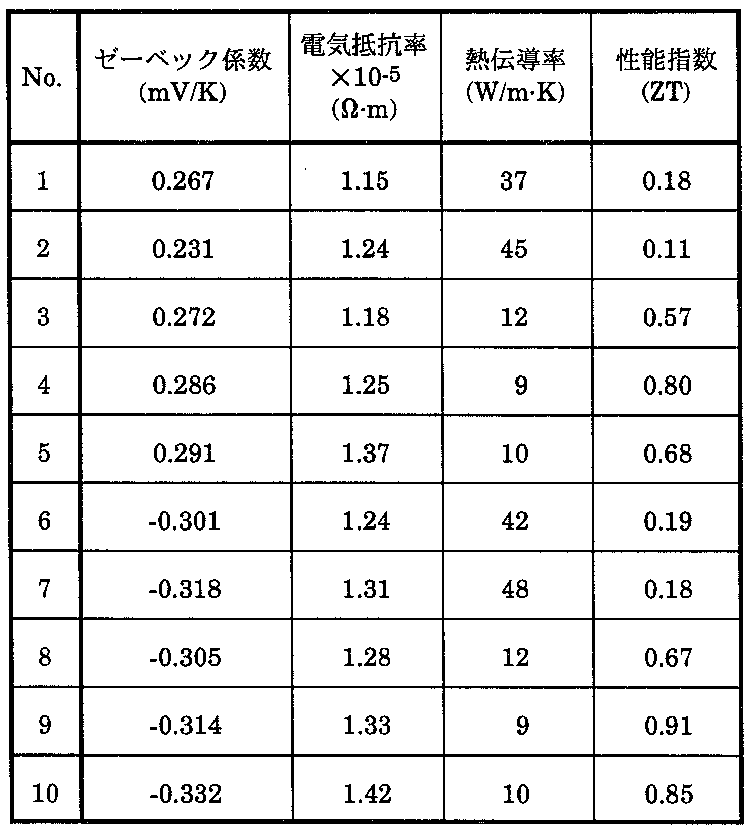
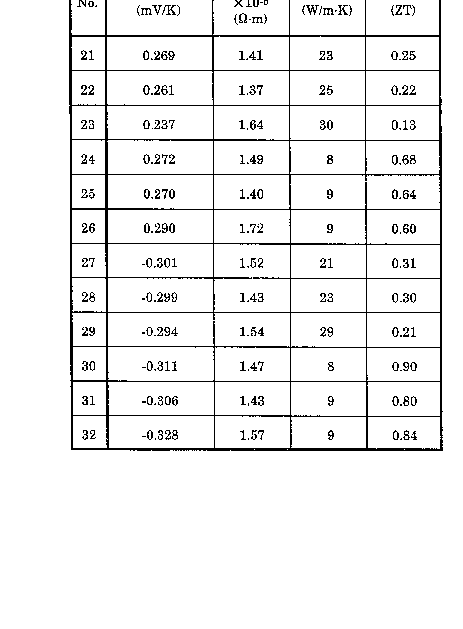
- a value measured at 1100K, a figure of merit (ZT S 2 T / P K) shown in Table 10.
- thermoelectric semiconductors To produce p-type and n-type Si thermoelectric semiconductors, high-purity Si (lON) and additive elements are mixed as shown in Table 11, and then vacuum melted in a high-frequency melting furnace using a graphite crucible. did.
- the molten metal was discharged from a nozzle having an inner diameter of 3 mm and quenched by blowing Ar gas at 3 MPa on the molten metal to obtain a spherical atomized powder having an average particle diameter of 30 to: ⁇ .
- the cooling rate of the atomized powder was 500 to: LOOOK / sec, and the average crystal grain size was 1 to 30 ⁇ .
- the obtained atomized powder was subjected to discharge plasma sintering in an Ar atmosphere.
- the sintering was performed at 1325 KX for 3 minutes.
- the sintered body samples were cut into 5X5X15mm, 10X10X2mm, and 10X2mm outer diameters, and the Seebeck coefficient, Hall coefficient (including carrier concentration and electrical conductivity), and thermal conductivity were determined as in Example 4. It measured by the same method.
- a plate-shaped ingot was obtained by embedding into a 10 mm thick mold. Thereafter, the ingot was pulverized, and further pulverized with a stamp mill and a jet mill to an average particle size of 1 to 10 ⁇ . Jet mill (using iN 2 gas at a pressure of 0.7 MPa).
- the obtained powder (base particles) is placed in a chamber and subjected to plasma treatment with SiH 4 gas or GeH 4 gas, and additional elements that generate carriers such as B, Al, Ga, P, As, and Sb in the powder Was coated with the film thickness shown in Table 15.
- Example 9 It was compression molded into a shape of 10 2111111 with a pressure of 200] ⁇ 5 &, and sintered in vacuum at 1325KX5h.
- high-purity Si (lON) was vacuum-melted in a high-frequency melting furnace using a graphite crucible. After dissolution, it was poured into a 10 mm thick mold to obtain a plate-like ingot. Thereafter, the ingot was pulverized, and further pulverized with a stamp mill and a ball mill to an average particle size of 10 to 50 ⁇ .
- the ball mill used a wet xylene solvent.
- the additive elements for producing the child particles to be coated on the periphery of Si were blended as shown in Table 17, and then melted in a high-frequency melting furnace using a graphite crucible.
- the melt was discharged from a nozzle with an inner diameter of 3 mm, and the melt was quenched by blowing Ar gas at 3 MPa, and the average particle size was 30 to: ⁇ .
- the obtained base particles were coated with child particles by mechanofusion so that the child particles had a predetermined weight ratio.
- the coated raw material powder was subjected to spark plasma sintering in an Ar atmosphere.
- the sintering conditions were 1325 KX 180 sec.
- the sintered sample is 5x5 15mm,
- Si and (lll) Ueha inserted into the vacuum chamber in one of 10- 6 Torr, 50 times deposited elements shown in Table 19 by an electron beam heating alternately thickness shown in Tables 19 as the A layer and the B layer, Laminated.
- the obtained sample on the wafer was cut into a shape of 5X15mm, 10X10mm and outer diameter of 10mm, and its Seebeck coefficient, Hall coefficient (including carrier concentration and electrical conductivity), Thermal conductivity was measured with the Si wafer.
- a value measured at 1100K, a figure of merit (ZT S 2 T / pK ) shown in Table 20.
- the Seebeck coefficient is a value obtained by measuring the thermoelectromotive force of the sample with a digital multimeter and setting the temperature difference between the high and low temperature sections to approximately 6K while increasing the temperature, and then dividing by the temperature difference. Asked.
- the Hall coefficient was measured by the AC method, and the electrical resistance was measured by the four-terminal method simultaneously with the carrier concentration.
- the thermal conductivity was measured by a laser flash method.
- the Si (lll) wafer was introduced into a vacuum chamber of 10-2 Torr, and the elements shown in Table 21 were alternately formed into layers A and B with the thickness shown in Table 1 by sputtering 50 times, and laminated by sputtering.
- Table 21 The Si (lll) wafer was introduced into a vacuum chamber of 10-2 Torr, and the elements shown in Table 21 were alternately formed into layers A and B with the thickness shown in Table 1 by sputtering 50 times, and laminated by sputtering.
- the obtained sample on the wafer is cut into a shape of 5 x 15 mm, 10 x 10 mm, outer diameter 10 mm, and its Seebeck coefficient, Hall coefficient (including carrier concentration and electrical conductivity), and heat conductivity
- the rate was measured together with the Si wafer.
- a value measured at 1100K, a figure of merit (ZT S 2 T / pK ) shown in Table 22.
- thermoelectric semiconductors To produce p-type Si-based thermoelectric semiconductors, high-purity Si (lON) and Group IV elements
- the temperature difference between the high and low temperature sections was set to 6K, and the thermoelectromotive force of the P-type semiconductor at an average temperature of 200 ° C between the high and low temperature sections was measured with a digital multimeter. Later, it was calculated as a value divided by the temperature difference (6K).
- the Hall coefficient was measured by applying an alternating magnetic field of 0.4 T at 437 K, and the electrical resistivity was measured by the four-terminal method simultaneously with the carrier concentration. Furthermore, the thermal conductivity is determined by the laser flash method.
- Z S 2 / pK.
- Si-Ge alloy (Ge30at% ») and Si without added Ge are described as comparative materials.
- buttons, C, Sn, an additive element that does not generate a carrier, Bnc and a Group V element (additive elements that generate a carrier, ⁇ , ⁇ ) were mixed as shown in Table 24, and then arc-melted in an Ar gas atmosphere.
- the obtained button-shaped ingot is 5X 5X 5mm,
- thermoelectric semiconductors In order to produce p-type and n-type Si-based thermoelectric semiconductors, high-purity Si (lON), Group IV elements (Ge, C, Sn, additive elements that do not generate carriers Bncl), and Group m-V compounds A conductor (GaP, GsP) or a Group III-VI compound semiconductor (ZnS) (compound semiconductor is an additive element Bnc2 which does not generate a carrier), and a Group III element, a Group m element or a Group V element which generates a carrier; After the Group VI elements were blended as shown in Table 25, they were melted in a high-frequency melting furnace in a 40 kPa Ar gas atmosphere.
- Group VI elements were blended as shown in Table 25, they were melted in a high-frequency melting furnace in a 40 kPa Ar gas atmosphere.
- the obtained ingot was cut into a shape of 5X5X5mm, 10X10X2mm, 10 ⁇ 2 ⁇ , and the Zelleta coefficient (S), Hall coefficient (Carrier concentration (n) and electrical resistivity (P) were determined, respectively. And thermal conductivity ( ⁇ ).
- the spark plasma sintering device used was SPS-2040 manufactured by Izmitek.
- the obtained sintered body was cut into a shape of 5X5X5mm, 10X10X2mm and outer diameter of 10X2mm. Produced.
- the Seebeck coefficient is set as pt for the high-temperature part electrode and Pt for the low-temperature part electrode, and the temperature difference between them is set to 6K, and the thermoelectric power of the P-type semiconductor at an average temperature of 323K between the high-temperature part and the low-temperature part is measured. After that, the thermoelectromotive force was calculated as a value obtained by dividing by 6K.
- the Hall coefficient was measured by the AC method at 323 K, and at that time, the electrical resistivity was also measured by the four-terminal method. Furthermore, the thermal conductivity was measured at 323 K by the laser-flash method. Tables 30 and 31 show the measurement results.
- thermoelectric conversion material according to the present invention is very advantageous as a thermoelectric conversion element for an automobile because Si as a main component is excellent in global environment, global resources and safety, and has a small specific gravity and light weight. Since bulk Si has excellent corrosion resistance, it has the advantage of not requiring surface treatment or the like.
- thermoelectric conversion material according to the present invention mainly uses Si, it is less expensive than a Si-Ge material containing a large amount of expensive Ge, and can obtain a higher performance index than that of the Fe-Si material. Furthermore, since Si used in the present invention has much lower purity than semiconductor devices, the raw material can be obtained at relatively low cost, and an inexpensive thermoelectric conversion material with good productivity and stable quality can be obtained.
- thermoelectric conversion material according to the present invention takes advantage of the characteristics of Si, which has a large Seebeck coefficient and a small electric resistance where the carrier concentration is high, and significantly reduces the defect of high thermal conductivity, and has a large figure of merit. This is an effective way to get the material.
- the physical property value can be controlled by the type and amount of the added element.
- thermoelectric varying ⁇ fee according to the invention containing at least one 5 to 10 atomic% »of Sn, as is apparent in the examples, zero one Beck coefficient ⁇ 2.0 ⁇ 4.0X 10- 4 V / K, which significantly lowers the thermal conductivity of the material to 50 (W / m'K) or less without lowering the inherent Seebeck coefficient of the new Si-based thermoelectric conversion material. Significant improvement of the index can be realized.
- thermoelectric conversion material according to the present invention having a porosity of 5 to 40% has a Seebeck coefficient of 0.07 to 0.200 X 10⁻⁴ V / K, and a novel Si-based thermoelectric conversion. Without significantly lowering the Seebeck coefficient of the material, the thermal conductivity of the material can be greatly reduced to 33 (W / m'K) or less, and a significant improvement in the figure of merit can be realized.
Landscapes
- Chemical & Material Sciences (AREA)
- Inorganic Chemistry (AREA)
- Silicon Compounds (AREA)
Description


Claims
Priority Applications (5)
| Application Number | Priority Date | Filing Date | Title |
|---|---|---|---|
| US09/674,978 US7002071B1 (en) | 1999-03-10 | 2000-03-10 | Thermoelectric conversion material and method of producing the same |
| CNB008005028A CN100385694C (zh) | 1999-03-10 | 2000-03-10 | 热电转换材料及其制作方法 |
| CA002331533A CA2331533A1 (en) | 1999-03-10 | 2000-03-10 | Thermoelectric conversion material and method of producing the same |
| AU29415/00A AU752619B2 (en) | 1999-03-10 | 2000-03-10 | Thermoelectric conversion material and method of producing the same |
| EP00908000A EP1083610A4 (en) | 1999-03-10 | 2000-03-10 | THERMOELECTRIC CONVERSION MATERIAL AND MANUFACTURING METHOD THEREFOR |
Applications Claiming Priority (10)
| Application Number | Priority Date | Filing Date | Title |
|---|---|---|---|
| JP11063093A JP2000261045A (ja) | 1999-03-10 | 1999-03-10 | 熱電変換材料の製造方法 |
| JP11/63093 | 1999-03-10 | ||
| JP11063074A JP2000261043A (ja) | 1999-03-10 | 1999-03-10 | 熱電変換材料とその製造方法 |
| JP11063088A JP2000261044A (ja) | 1999-03-10 | 1999-03-10 | 熱電変換材料とその製造方法 |
| JP1163099 | 1999-03-10 | ||
| JP11/63074 | 1999-03-10 | ||
| JP11/63099 | 1999-03-10 | ||
| JP11/63088 | 1999-03-10 | ||
| JP11/243118 | 1999-08-30 | ||
| JP24311899A JP2001068744A (ja) | 1999-08-30 | 1999-08-30 | 熱電変換材料と熱電変換素子 |
Publications (1)
| Publication Number | Publication Date |
|---|---|
| WO2000054343A1 true WO2000054343A1 (fr) | 2000-09-14 |
Family
ID=27519307
Family Applications (1)
| Application Number | Title | Priority Date | Filing Date |
|---|---|---|---|
| PCT/JP2000/001469 Ceased WO2000054343A1 (fr) | 1999-03-10 | 2000-03-10 | Materiau de conversion thermoelectrique et procede de production associe |
Country Status (1)
| Country | Link |
|---|---|
| WO (1) | WO2000054343A1 (ja) |
Cited By (3)
| Publication number | Priority date | Publication date | Assignee | Title |
|---|---|---|---|---|
| US20090223548A1 (en) * | 2005-03-14 | 2009-09-10 | Borealis Technical Limited | Thermionic/Thermotunneling Thermo-Electrical Converter |
| JP2017050505A (ja) * | 2015-09-04 | 2017-03-09 | 株式会社日立製作所 | 熱電変換材料および熱電変換モジュール |
| JP2018190906A (ja) * | 2017-05-10 | 2018-11-29 | 株式会社日立製作所 | 熱電変換材料及び熱電変換モジュール |
Citations (3)
| Publication number | Priority date | Publication date | Assignee | Title |
|---|---|---|---|---|
| JPS61149453A (ja) * | 1984-12-08 | 1986-07-08 | ザ ユニバーシテイ コート オブ ザ ユニバーシテイ オブ グラスゴウ | 熱電合金ならびにこれを用いた熱電半導体材料および熱電装置 |
| JPH06216414A (ja) * | 1993-01-21 | 1994-08-05 | Idemitsu Petrochem Co Ltd | 熱電変換材料の製造法 |
| JPH10242535A (ja) * | 1997-02-27 | 1998-09-11 | Central Res Inst Of Electric Power Ind | 熱電材料及びその製造方法 |
-
2000
- 2000-03-10 WO PCT/JP2000/001469 patent/WO2000054343A1/ja not_active Ceased
Patent Citations (3)
| Publication number | Priority date | Publication date | Assignee | Title |
|---|---|---|---|---|
| JPS61149453A (ja) * | 1984-12-08 | 1986-07-08 | ザ ユニバーシテイ コート オブ ザ ユニバーシテイ オブ グラスゴウ | 熱電合金ならびにこれを用いた熱電半導体材料および熱電装置 |
| JPH06216414A (ja) * | 1993-01-21 | 1994-08-05 | Idemitsu Petrochem Co Ltd | 熱電変換材料の製造法 |
| JPH10242535A (ja) * | 1997-02-27 | 1998-09-11 | Central Res Inst Of Electric Power Ind | 熱電材料及びその製造方法 |
Non-Patent Citations (1)
| Title |
|---|
| See also references of EP1083610A4 * |
Cited By (4)
| Publication number | Priority date | Publication date | Assignee | Title |
|---|---|---|---|---|
| US20090223548A1 (en) * | 2005-03-14 | 2009-09-10 | Borealis Technical Limited | Thermionic/Thermotunneling Thermo-Electrical Converter |
| US8541678B2 (en) * | 2005-03-14 | 2013-09-24 | Borealis Technical Limited | Thermionic/thermotunneling thermo-electrical converter |
| JP2017050505A (ja) * | 2015-09-04 | 2017-03-09 | 株式会社日立製作所 | 熱電変換材料および熱電変換モジュール |
| JP2018190906A (ja) * | 2017-05-10 | 2018-11-29 | 株式会社日立製作所 | 熱電変換材料及び熱電変換モジュール |
Similar Documents
| Publication | Publication Date | Title |
|---|---|---|
| KR100419488B1 (ko) | 열전 변환 재료 및 그 제조 방법 | |
| JP4399757B2 (ja) | 熱電変換材料とその製造方法 | |
| CN1969354B (zh) | 制造锰铝铜强磁性合金、半锰铝铜强磁性合金、填充式方钴矿基合金的方法以及利用它们的热电转换系统 | |
| US8173093B2 (en) | Iron silicide sputtering target and method for production thereof | |
| KR100924054B1 (ko) | 열전 재료 및 그 제조 방법 | |
| EP0874406A2 (en) | A co-sb based thermoelectric material and a method of producing the same | |
| US6506321B1 (en) | Silicon based conductive material and process for production thereof | |
| JP2002064227A (ja) | 熱電変換材料とその製造方法 | |
| TWI775887B (zh) | 熱電轉換材料、熱電轉換元件、熱電轉換模組及熱電轉換材料之製造方法 | |
| US8753529B2 (en) | Clathrate compound, thermoelectric material, and method for producing thermoelectric material | |
| JP2004076046A (ja) | フィルドスクッテルダイト系合金、その製造方法および熱電変換素子 | |
| Zhao et al. | Effects of process parameters on electrical properties of n-type Bi2Te3 prepared by mechanical alloying and spark plasma sintering | |
| JP5768446B2 (ja) | 珪化バリウム多結晶体、その製造方法ならびに珪化バリウムスパッタリングターゲット | |
| JP7562093B2 (ja) | 珪化物系合金薄膜及びその製造方法 | |
| WO2000054343A1 (fr) | Materiau de conversion thermoelectrique et procede de production associe | |
| JP2000261044A (ja) | 熱電変換材料とその製造方法 | |
| JP2000261043A (ja) | 熱電変換材料とその製造方法 | |
| JP2006086512A (ja) | フィルドスクッテルダイト系合金を用いた熱電変換システム。 | |
| JP2000261045A (ja) | 熱電変換材料の製造方法 | |
| JP7655309B2 (ja) | 熱電変換素子の製造方法 | |
| JP2001068744A (ja) | 熱電変換材料と熱電変換素子 | |
| Kim et al. | Fabrication and Characterization of Thermoelectric Thick Film Prepared from p-Type Bismuth Telluride Nanopowders | |
| TW201718900A (zh) | 合金材料與其製造方法、以及熱電轉換元件 | |
| JP2001144336A (ja) | 熱電変換材料とその製造方法 | |
| JP2018160620A (ja) | 熱電変換材料及びその製造方法、並びに、熱電変換素子、熱電変換モジュール、移動体 |
Legal Events
| Date | Code | Title | Description |
|---|---|---|---|
| WWE | Wipo information: entry into national phase |
Ref document number: 00800502.8 Country of ref document: CN |
|
| AK | Designated states |
Kind code of ref document: A1 Designated state(s): AU CA CN KR US |
|
| AL | Designated countries for regional patents |
Kind code of ref document: A1 Designated state(s): AT BE CH CY DE DK ES FI FR GB GR IE IT LU MC NL PT SE |
|
| 121 | Ep: the epo has been informed by wipo that ep was designated in this application | ||
| ENP | Entry into the national phase |
Ref document number: 2331533 Country of ref document: CA |
|
| WWE | Wipo information: entry into national phase |
Ref document number: 09674978 Country of ref document: US |
|
| WWE | Wipo information: entry into national phase |
Ref document number: 29415/00 Country of ref document: AU Ref document number: 1020007012611 Country of ref document: KR |
|
| WWE | Wipo information: entry into national phase |
Ref document number: 2000908000 Country of ref document: EP |
|
| WWP | Wipo information: published in national office |
Ref document number: 2000908000 Country of ref document: EP |
|
| WWP | Wipo information: published in national office |
Ref document number: 1020007012611 Country of ref document: KR |
|
| WWG | Wipo information: grant in national office |
Ref document number: 29415/00 Country of ref document: AU |
|
| WWG | Wipo information: grant in national office |
Ref document number: 1020007012611 Country of ref document: KR |