WO2003087228A1 - Composition of silicon-containing copolymer, solvent-soluble crosslinked silicon-containing copolymer, and cured articles obtained therefrom - Google Patents
Composition of silicon-containing copolymer, solvent-soluble crosslinked silicon-containing copolymer, and cured articles obtained therefrom Download PDFInfo
- Publication number
- WO2003087228A1 WO2003087228A1 PCT/JP2003/004336 JP0304336W WO03087228A1 WO 2003087228 A1 WO2003087228 A1 WO 2003087228A1 JP 0304336 W JP0304336 W JP 0304336W WO 03087228 A1 WO03087228 A1 WO 03087228A1
- Authority
- WO
- WIPO (PCT)
- Prior art keywords
- silicon
- group
- containing copolymer
- solvent
- film
- Prior art date
- Legal status (The legal status is an assumption and is not a legal conclusion. Google has not performed a legal analysis and makes no representation as to the accuracy of the status listed.)
- Ceased
Links
Classifications
-
- H—ELECTRICITY
- H01—ELECTRIC ELEMENTS
- H01J—ELECTRIC DISCHARGE TUBES OR DISCHARGE LAMPS
- H01J11/00—Gas-filled discharge tubes with alternating current induction of the discharge, e.g. alternating current plasma display panels [AC-PDP]; Gas-filled discharge tubes without any main electrode inside the vessel; Gas-filled discharge tubes with at least one main electrode outside the vessel
- H01J11/10—AC-PDPs with at least one main electrode being out of contact with the plasma
- H01J11/12—AC-PDPs with at least one main electrode being out of contact with the plasma with main electrodes provided on both sides of the discharge space
-
- C—CHEMISTRY; METALLURGY
- C08—ORGANIC MACROMOLECULAR COMPOUNDS; THEIR PREPARATION OR CHEMICAL WORKING-UP; COMPOSITIONS BASED THEREON
- C08G—MACROMOLECULAR COMPOUNDS OBTAINED OTHERWISE THAN BY REACTIONS ONLY INVOLVING UNSATURATED CARBON-TO-CARBON BONDS
- C08G77/00—Macromolecular compounds obtained by reactions forming a linkage containing silicon with or without sulfur, nitrogen, oxygen or carbon in the main chain of the macromolecule
- C08G77/48—Macromolecular compounds obtained by reactions forming a linkage containing silicon with or without sulfur, nitrogen, oxygen or carbon in the main chain of the macromolecule in which at least two but not all the silicon atoms are connected by linkages other than oxygen atoms
- C08G77/54—Nitrogen-containing linkages
-
- C—CHEMISTRY; METALLURGY
- C08—ORGANIC MACROMOLECULAR COMPOUNDS; THEIR PREPARATION OR CHEMICAL WORKING-UP; COMPOSITIONS BASED THEREON
- C08J—WORKING-UP; GENERAL PROCESSES OF COMPOUNDING; AFTER-TREATMENT NOT COVERED BY SUBCLASSES C08B, C08C, C08F, C08G or C08H
- C08J5/00—Manufacture of articles or shaped materials containing macromolecular substances
- C08J5/18—Manufacture of films or sheets
-
- C—CHEMISTRY; METALLURGY
- C08—ORGANIC MACROMOLECULAR COMPOUNDS; THEIR PREPARATION OR CHEMICAL WORKING-UP; COMPOSITIONS BASED THEREON
- C08J—WORKING-UP; GENERAL PROCESSES OF COMPOUNDING; AFTER-TREATMENT NOT COVERED BY SUBCLASSES C08B, C08C, C08F, C08G or C08H
- C08J5/00—Manufacture of articles or shaped materials containing macromolecular substances
- C08J5/20—Manufacture of shaped structures of ion-exchange resins
- C08J5/22—Films, membranes or diaphragms
-
- C—CHEMISTRY; METALLURGY
- C08—ORGANIC MACROMOLECULAR COMPOUNDS; THEIR PREPARATION OR CHEMICAL WORKING-UP; COMPOSITIONS BASED THEREON
- C08L—COMPOSITIONS OF MACROMOLECULAR COMPOUNDS
- C08L83/00—Compositions of macromolecular compounds obtained by reactions forming in the main chain of the macromolecule a linkage containing silicon with or without sulfur, nitrogen, oxygen or carbon only; Compositions of derivatives of such polymers
- C08L83/14—Compositions of macromolecular compounds obtained by reactions forming in the main chain of the macromolecule a linkage containing silicon with or without sulfur, nitrogen, oxygen or carbon only; Compositions of derivatives of such polymers in which at least two but not all the silicon atoms are connected by linkages other than oxygen atoms
-
- C—CHEMISTRY; METALLURGY
- C09—DYES; PAINTS; POLISHES; NATURAL RESINS; ADHESIVES; COMPOSITIONS NOT OTHERWISE PROVIDED FOR; APPLICATIONS OF MATERIALS NOT OTHERWISE PROVIDED FOR
- C09D—COATING COMPOSITIONS, e.g. PAINTS, VARNISHES OR LACQUERS; FILLING PASTES; CHEMICAL PAINT OR INK REMOVERS; INKS; CORRECTING FLUIDS; WOODSTAINS; PASTES OR SOLIDS FOR COLOURING OR PRINTING; USE OF MATERIALS THEREFOR
- C09D183/00—Coating compositions based on macromolecular compounds obtained by reactions forming in the main chain of the macromolecule a linkage containing silicon, with or without sulfur, nitrogen, oxygen, or carbon only; Coating compositions based on derivatives of such polymers
- C09D183/14—Coating compositions based on macromolecular compounds obtained by reactions forming in the main chain of the macromolecule a linkage containing silicon, with or without sulfur, nitrogen, oxygen, or carbon only; Coating compositions based on derivatives of such polymers in which at least two but not all the silicon atoms are connected by linkages other than oxygen atoms
-
- C—CHEMISTRY; METALLURGY
- C09—DYES; PAINTS; POLISHES; NATURAL RESINS; ADHESIVES; COMPOSITIONS NOT OTHERWISE PROVIDED FOR; APPLICATIONS OF MATERIALS NOT OTHERWISE PROVIDED FOR
- C09D—COATING COMPOSITIONS, e.g. PAINTS, VARNISHES OR LACQUERS; FILLING PASTES; CHEMICAL PAINT OR INK REMOVERS; INKS; CORRECTING FLUIDS; WOODSTAINS; PASTES OR SOLIDS FOR COLOURING OR PRINTING; USE OF MATERIALS THEREFOR
- C09D183/00—Coating compositions based on macromolecular compounds obtained by reactions forming in the main chain of the macromolecule a linkage containing silicon, with or without sulfur, nitrogen, oxygen, or carbon only; Coating compositions based on derivatives of such polymers
- C09D183/16—Coating compositions based on macromolecular compounds obtained by reactions forming in the main chain of the macromolecule a linkage containing silicon, with or without sulfur, nitrogen, oxygen, or carbon only; Coating compositions based on derivatives of such polymers in which all the silicon atoms are connected by linkages other than oxygen atoms
-
- H—ELECTRICITY
- H01—ELECTRIC ELEMENTS
- H01J—ELECTRIC DISCHARGE TUBES OR DISCHARGE LAMPS
- H01J11/00—Gas-filled discharge tubes with alternating current induction of the discharge, e.g. alternating current plasma display panels [AC-PDP]; Gas-filled discharge tubes without any main electrode inside the vessel; Gas-filled discharge tubes with at least one main electrode outside the vessel
- H01J11/20—Constructional details
- H01J11/34—Vessels, containers or parts thereof, e.g. substrates
- H01J11/36—Spacers, barriers, ribs, partitions or the like
-
- H—ELECTRICITY
- H01—ELECTRIC ELEMENTS
- H01J—ELECTRIC DISCHARGE TUBES OR DISCHARGE LAMPS
- H01J11/00—Gas-filled discharge tubes with alternating current induction of the discharge, e.g. alternating current plasma display panels [AC-PDP]; Gas-filled discharge tubes without any main electrode inside the vessel; Gas-filled discharge tubes with at least one main electrode outside the vessel
- H01J11/20—Constructional details
- H01J11/34—Vessels, containers or parts thereof, e.g. substrates
- H01J11/38—Dielectric or insulating layers
-
- H—ELECTRICITY
- H01—ELECTRIC ELEMENTS
- H01J—ELECTRIC DISCHARGE TUBES OR DISCHARGE LAMPS
- H01J11/00—Gas-filled discharge tubes with alternating current induction of the discharge, e.g. alternating current plasma display panels [AC-PDP]; Gas-filled discharge tubes without any main electrode inside the vessel; Gas-filled discharge tubes with at least one main electrode outside the vessel
- H01J11/20—Constructional details
- H01J11/48—Sealing, e.g. seals specially adapted for leading-in conductors
-
- C—CHEMISTRY; METALLURGY
- C08—ORGANIC MACROMOLECULAR COMPOUNDS; THEIR PREPARATION OR CHEMICAL WORKING-UP; COMPOSITIONS BASED THEREON
- C08K—Use of inorganic or non-macromolecular organic substances as compounding ingredients
- C08K5/00—Use of organic ingredients
- C08K5/54—Silicon-containing compounds
- C08K5/541—Silicon-containing compounds containing oxygen
- C08K5/5415—Silicon-containing compounds containing oxygen containing at least one Si—O bond
-
- C—CHEMISTRY; METALLURGY
- C08—ORGANIC MACROMOLECULAR COMPOUNDS; THEIR PREPARATION OR CHEMICAL WORKING-UP; COMPOSITIONS BASED THEREON
- C08K—Use of inorganic or non-macromolecular organic substances as compounding ingredients
- C08K5/00—Use of organic ingredients
- C08K5/54—Silicon-containing compounds
- C08K5/544—Silicon-containing compounds containing nitrogen
- C08K5/5465—Silicon-containing compounds containing nitrogen containing at least one C=N bond
-
- G—PHYSICS
- G02—OPTICS
- G02F—OPTICAL DEVICES OR ARRANGEMENTS FOR THE CONTROL OF LIGHT BY MODIFICATION OF THE OPTICAL PROPERTIES OF THE MEDIA OF THE ELEMENTS INVOLVED THEREIN; NON-LINEAR OPTICS; FREQUENCY-CHANGING OF LIGHT; OPTICAL LOGIC ELEMENTS; OPTICAL ANALOGUE/DIGITAL CONVERTERS
- G02F1/00—Devices or arrangements for the control of the intensity, colour, phase, polarisation or direction of light arriving from an independent light source, e.g. switching, gating or modulating; Non-linear optics
- G02F1/01—Devices or arrangements for the control of the intensity, colour, phase, polarisation or direction of light arriving from an independent light source, e.g. switching, gating or modulating; Non-linear optics for the control of the intensity, phase, polarisation or colour
- G02F1/13—Devices or arrangements for the control of the intensity, colour, phase, polarisation or direction of light arriving from an independent light source, e.g. switching, gating or modulating; Non-linear optics for the control of the intensity, phase, polarisation or colour based on liquid crystals, e.g. single liquid crystal display cells
- G02F1/133—Constructional arrangements; Operation of liquid crystal cells; Circuit arrangements
- G02F1/1333—Constructional arrangements; Manufacturing methods
- G02F1/133345—Insulating layers
-
- H—ELECTRICITY
- H01—ELECTRIC ELEMENTS
- H01J—ELECTRIC DISCHARGE TUBES OR DISCHARGE LAMPS
- H01J2211/00—Plasma display panels with alternate current induction of the discharge, e.g. AC-PDPs
- H01J2211/20—Constructional details
- H01J2211/34—Vessels, containers or parts thereof, e.g. substrates
- H01J2211/36—Spacers, barriers, ribs, partitions or the like
- H01J2211/366—Spacers, barriers, ribs, partitions or the like characterized by the material
-
- Y—GENERAL TAGGING OF NEW TECHNOLOGICAL DEVELOPMENTS; GENERAL TAGGING OF CROSS-SECTIONAL TECHNOLOGIES SPANNING OVER SEVERAL SECTIONS OF THE IPC; TECHNICAL SUBJECTS COVERED BY FORMER USPC CROSS-REFERENCE ART COLLECTIONS [XRACs] AND DIGESTS
- Y10—TECHNICAL SUBJECTS COVERED BY FORMER USPC
- Y10T—TECHNICAL SUBJECTS COVERED BY FORMER US CLASSIFICATION
- Y10T428/00—Stock material or miscellaneous articles
- Y10T428/31504—Composite [nonstructural laminate]
- Y10T428/31652—Of asbestos
- Y10T428/31663—As siloxane, silicone or silane
Definitions
- Silicon-containing copolymer composition Silicon-containing copolymer composition, solvent-soluble crosslinked silicon-containing copolymer, and cured products thereof
- the present invention relates to a silicon-containing copolymer composition containing a crosslinking agent, a silicon-containing copolymer crosslinked by a crosslinking agent, and a heat-resistant and transparent heat-resistant and transparent copolymer comprising the silicon-containing copolymer.
- a film or coating having excellent flexibility, low dielectric constant, excellent flexibility and mechanical strength, and a cured product of the above-described silicon-containing copolymer composition is used as a dielectric layer, partition wall (rib layer) and
- the present invention relates to a plasma display device (PDP) having a vacuum sealing agent or a liquid crystal display device (LCD) having the cured product as an interlayer insulating film and / or an alignment film.
- PDP plasma display device
- LCD liquid crystal display device
- aromatic and heterocyclic polymers such as fluorine-based materials, polybenzimidazoles, aromatic polyamides, and polyimides have been studied since the synthesis of silicone by Rocho et al. I have. Furthermore, in recent years, the demand for heat resistance has increased along with the development of the space and aviation fields, research has been progressed on aromatic and heterocyclic polymers, and improvements in aromatic polyimides have been promoted.
- organic metal polymers whose main chains are composed of metal elements such as Si, Ti, and B and 0, N, such as polyporosiloxane and polytitanosiloxane, have been studied.
- heat-resistant and insulating materials used in various applications have recently been required to have further improved heat resistance.
- heat-resistant insulation materials One of the applications is in the field of high-voltage rotating machines such as generators, high-voltage AC motors, industrial DC motors, and train motors. Those belonging to these high-pressure rotating machines tend to have larger capacities and higher pressures, and are also required to be smaller and have higher heat resistance. Heat resistance in these fields ⁇ Some insulating materials are required to have a heat resistance exceeding 400 ° C in the air, and also need high insulation, flexibility, mechanical properties, etc. as well as heat resistance It is said.
- heat-resistant and insulating materials include insulation or dielectric layers for display devices such as PDPs and LCDs, interlayer insulating films for thin-film semiconductor devices, and low temperature process for 600 ° C pre-metal.
- Dielectric layer (PMD) materials and other semiconductor device materials front panels of display devices, heat-resistant films, heat-resistant sheets or coatings used in various applications, plastic optical fibers, heat-resistant and insulating yarns, electric wires Various ones, including coatings, may be mentioned.
- PMD Dielectric layer
- ceramic box composites Ceramic-metal adhesives, A l 2 ⁇ 3, fields such as high performance products by Purendo with high functionality products, other polymers with ceramic box material Mg O, etc. Attempts are also being made to use this material.
- organic polymers have a heat-resistant temperature of 300 ° C or less.
- organometallic polymers such as silicone resins and polysiloxane resins have a high heat resistance of 500 ° C. or higher because of the high thermal stability of the polymer.
- organic polymers have a linear structure with few branches in molecular structure
- organometallic polymers have a network structure with many branches, and are enormous due to the dehydrocondensation reaction or oxidation reaction between OH groups. Three-dimensional network structure, resulting in poor flexibility and limited use It was.
- the present inventor has developed and provided a high heat-resistant silicon-containing copolymer composed of a silazane copolymer containing a specific repeating unit (Japanese Patent Application Laid-Open No. Hei 8-23217). No. 27 and Japanese Patent Application Laid-Open No. 91-188765.
- This silicon-containing copolymer has heat resistance of 400 ° C or higher, is an organometallic polymer with excellent mechanical properties and flexibility, is easy to manufacture, and is transparent when cured in nitrogen. It has the following features. Therefore, although it is a useful material for high heat resistant optical applications, when cured in air, the resulting cured polymer is colored, and it is difficult to obtain a film with good transparency. For this reason, the above-mentioned silicon-containing copolymer needs to be cured in nitrogen in order to obtain a transparent cured polymer, and it is sometimes difficult to apply it to applications from the viewpoint of process cost and mass production.
- the inventor of the present invention has disclosed a PDP in which the fired film of the silicon-containing copolymer proposed in Japanese Patent Application No. 2001-99092 is used as a dielectric layer for covering a transparent electrode or an address electrode.
- the application was filed as request 201-109485 (Japanese Patent Application Laid-Open No. 2002-304949).
- the curing temperature of the silicon-containing copolymer is as high as about 400 ° C.
- a cured product of the above-mentioned silicon-containing copolymer is used as a material for forming various coatings such as LCD and PDP or as a material for a sealing material, a curing temperature of 2 in a manufacturing process for LCD and PDP.
- the temperature be 50 ° C. or lower.
- the polymer which requires curing at 350 ° C. or higher cannot be used. If the curing temperature of the polymer can be set to 250 ° C. or lower, it can be applied to almost all FPD applications such as LCD and PDP, and the utility increases. Further, the polymer has room for improvement by further improving chemical resistance such as alkali resistance. Further, heat resistance, mechanical properties, flexibility, transparency, relative permittivity, etc. are required to be further improved as compared with conventional ones. There is also a need for a material that can further increase the thickness of a coating film formed by one application.
- An object of the present invention is to solve the above-mentioned problems, that is, it can be cured at a low temperature, has colorless and high transparency even when cured in the air, has heat resistance of 400 ° C. or more, and particularly has a reduced pressure.
- a silicon-containing copolymer composition which is resistant to heating at a temperature of 400 ° C. or more below and which can form a film or coating having high chemical resistance and low relative dielectric constant;
- An object of the present invention is to provide a crosslinked silicon-containing copolymer which is partially crosslinked and is soluble in a solvent, formed from the product.
- an object of the present invention is to form a film or a coating film having the above-mentioned characteristics, which has a large thickness formed by one application, and has excellent mechanical strength and flexibility. It is an object of the present invention to provide a partially crosslinked silicon-containing copolymer and a silicon-containing copolymer composition used for forming the partially crosslinked silicon-containing copolymer.
- an object of the present invention is to provide a method for curing the above composition or the above-mentioned solvent-soluble crosslinked silicon-containing copolymer, a film or a film having excellent heat resistance, chemical resistance and transparency, and having a low dielectric constant, or such a method.
- An object of the present invention is to provide a display device such as a liquid crystal display device (LCD) used as an alignment film or an alignment film, or a semiconductor device having the crosslinked silicon-containing copolymer as a layer constituting material. Disclosure of the invention
- the present inventor has found that heat resistance, transparency, and dielectric properties are maintained without coloring even when cured in the atmosphere proposed in the aforementioned Japanese Patent Application No. 2001-99092.
- the lowering of the curing temperature and the improvement of heat resistance and chemical resistance under reduced pressure, which were mentioned as the points of improvement of silicon-containing copolymer excellent in The present invention has been found to be solved by use in combination with a cross-linking agent which forms a bond with a polymer by reacting with a suitable water. That is, the present invention has the following configuration.
- a silicon-containing copolymer composition comprising a polymer and a crosslinking agent.
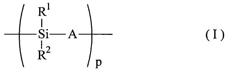
- R 1 R 2 , R 3 , R 4 , R 5 and R 6 each independently represent an alkyl group, an alkenyl group, a cycloalkyl group, an aryl group, an aralkyl group.
- R 7 represents a divalent group
- A represents NH or O.
- the structural units (I) and (II) are random, and their molar ratios p and q are arbitrary numbers excluding zero, and are S i —O bonds and S i —N bonds in the copolymer. The percentage of
- R 8 and R 9 each independently represent an alkyl group, an alkenyl group, a cycloalkyl group, an aryl group, an aralkyl group, an alkylamino group, an alkylsilyl group or an alkoxy group, and A represents NH or O.
- A represents NH or O.
- the structural units (I) to (IV) in the polymer are random, and the respective molar ratios p, q, r and s have the following relationship.
- RR 2 , R 8, and R 9 are each independently an alkyl group, an alkylene group, a cycloalkyl group, an aryl group, an aranolequinole group, an alkynoleamino group, an alkylsilyl group, or an alkoxy group.
- R 10 is a divalent aromatic group.
- the structural units (V) to (VII) are random, and t, u, and w are any numbers except zero. ]
- R 11 is a halogen atom or a lower alkyl group; a is an integer of 0 to 4; Z is a direct bond or a group represented by the following general formula (B).
- R 12 is a halogen atom or a lower alkyl group
- b is an integer of 0 to 4
- Y is a direct bond or a divalent group.
- a crosslinked silicon-containing copolymer formed by heating the silicon-containing copolymer composition according to any of [1] to [10].
- a silicon-containing copolymer characterized by heating the silicon-containing copolymer composition according to any of [1] to [10] above at a temperature of 150 ° C or more. Curing method.
- a crosslinked cured product of the silicon-containing copolymer composition according to any one of the above [1] to [10] is combined with a dielectric layer, partition walls (rib layers), and Z or a vacuum sealant. And a plasma display device.
- a liquid crystal display device comprising a crosslinked cured product of the silicon-containing copolymer composition according to any one of [1] to [10] as an interlayer insulating film and a Z or alignment film.
- a silicon-containing copolymer composition and a solvent-soluble crosslinked silicon-containing copolymer including the following embodiments as more preferred embodiments.
- Kei-containing copolymer composition or a solvent-soluble crosslinking Kei-containing copolymer polymer are each independently a methyl group or phenyl group
- R 7 and R 1 In the structural units of the general formulas (II) and (V) to (VII), R 7 and R 1 .
- the silicon-containing copolymer composition or the solvent-soluble crosslinked silicon-containing copolymer of the present invention is cured by heating after forming a film by being applied to an appropriate substrate or by heating after casting. It is used in the form of a molded article formed by curing. Since the cured product has heat resistance, it is used as a general heat-resistant material or a heat-resistant layer or as a hard coating film. In addition to these, the cured product has a low dielectric constant, is colorless and transparent, has high mechanical strength, and has chemical resistance such as alkali resistance Since it has characteristics such as excellent properties, it can be used or used in the following manner, for example.
- FIG. 1 is a schematic cross-sectional view of an AC plasma display panel having a dielectric layer formed using a cured film of the solvent-soluble crosslinked silicon-containing copolymer of the present invention. Detailed description of the invention
- the solvent-soluble or solvent-insoluble crosslinked silicon-containing copolymer of the present invention has the structural units of the general formulas (I) and (II), or It has structural units of general formulas (I) and (II) and at least one type of structural unit represented by general formulas (III) to (VII), and has a number average molecular weight of 500 to Silicon-containing copolymers in the range of 1, 000, 000
- Whether the crosslinking and curing proceeds to form a solvent-insoluble cured product depends on the heating temperature and heating time, the type and amount of the crosslinking agent, and the type and amount of the crosslinking accelerator if a crosslinking accelerator is used. It depends on various factors.
- cross-linking to produce a solvent-soluble cross-linked silicone-containing copolymer is usually performed by dissolving a base polymer, a cross-linking agent, and, if necessary, other additives such as a crosslinking accelerator in a solvent.
- the reaction is performed at an appropriate temperature, for example, a temperature of 120 to 100 ° C. Therefore, when producing the copolymer soluble in a solvent-soluble cross-linked silicon, heating may not be performed, and heating may be performed if necessary.
- the reaction time may be appropriately set depending on the reaction temperature.For example, when the reaction is performed under heating, the reaction time is usually 1 to
- the solvent-soluble cross-linked silicone-containing copolymer obtained by this cross-linking reaction is applied to, for example, a substrate, and then heated (baked) to a temperature at which cross-linking proceeds and hardening occurs, for example, a temperature of 150 ° C or more.
- the cured product is obtained.
- the cured product obtained in this way has excellent properties such as heat resistance, mechanical strength, transparency, insulation (dielectric properties), and chemical resistance, and is used in various applications as described above. be able to.
- the temperature at which the cured product is obtained depends on the type of the base polymer used, the type of the cross-linking agent, and the type of the cross-linking accelerator if a cross-linking accelerator is used.
- a cross-linking agent for example, as a cross-linking agent,
- the crosslinking agent decomposes at 150 ° C and curing begins.
- the lower limit of the cross-linking curing temperature in the present invention is not particularly limited as long as a cured product is obtained, but the cross-linking curing temperature may be usually 150 ° C. or higher. In order to carry out the curing more completely, it is usually more preferable to carry out the curing at a higher temperature, for example, at a temperature of 200 ° C. or more, and more preferably to about 250 ° C.
- the cross-linking reaction includes, in addition to those in which two or more silicon-containing copolymer molecules are cross-linked by a cross-linking agent, those in which the cross-linking agent is reacted with one silicon-containing copolymer, That is, the cross-linking agent also includes one added to the silicon-containing copolymer. Therefore, in the case of a solvent-soluble cross-linked silicon-containing copolymer, the cross-linking agent is one of the silicon-containing copolymers. It also includes a crosslinkable silicon-containing copolymer bonded to the polymer.
- the base polymer used in the silicon-containing copolymer composition of the present invention will be further described.
- the base polymer used for producing the solvent-soluble or solvent-insoluble cured cross-linked silicon-containing copolymer of the present invention is represented by the above general formula (11), and optionally (V) to (VII). Having the structural unit represented.
- R 7 bifunctional group
- the cured polymer obtained by curing has not only heat resistance of 400 ° C.
- the bonding order of the structural units of the general formulas (I) to (VII) is random, and the ratio p, q, r, s or p, q, r, s, t, u, w can usually take the following ranges.
- r / (p + q + r + s) 0 to 0.99, preferably 0.01 to 0.
- s no (p + q + r + s) 0 to 0.99, preferably 0.1 to 0.5 or
- the base polymer may be produced by any method.
- a preferred production method is represented by the following general formula (VIII):
- R 2 (wherein, R and R 2 are as defined above, and X represents a halogen atom.)
- R 8 and X are as defined above.
- R 9 and X are as defined above.
- 3 ⁇ 4 9 is an alkyl group, an alkenyl group, a cycloalkyl group, Ariru group, Ararukiru group, but selected from alkylamino amino group, an alkylsilyl group or an alkoxy group, usually 1 to carbon atoms 7, preferably 1 to 5 More preferably, an alkyl group having 1 to 2 carbon atoms, an alkenyl group having 2 to 7 carbon atoms, a cycloalkyl group having 5 to 7 carbon atoms, and an aryl group are generally used, and X is usually fluorine, chlorine, or bromine. And an iodine atom, preferably a chlorine atom.
- the aryl groups include phenyl, tolyl, xylinole, tamenyl, benzinole, phenethyl, ⁇ -methylbenzinole, benzhydryl, trityl, styryl, cinnamyl , A biphenyl group, a naphthyl group and the like.
- the alkylsilyl group mono-, di- or tri-substituted
- the alkylamino group (mono- or di-substituted) and the alkoxy group those having 1 to 7 carbon atoms are usually used. Is done.
- R 1 and R 2 may be the same or different, respectively.
- the compound represented by the general formula (VIII) is preferably diphenyl-dichlorosilane, and the compound represented by the general formula (X) is preferably methyldichlorosilane.
- ferrichlorosilane is preferred.
- R 3 to R 6 of the disilyl compound represented by the general formula (IX) used as a starting material when producing the silicon-containing copolymer in the present invention are represented by the general formulas (VIII), (VIII) X) and I 1, R 2, R 8 and R 9 same as in (XI), an alkyl group, an alkenyl group, a cycloalkyl group, Ariru group, ⁇ La alkyl group, an alkylamino group, alkylsilyl group or an alkoxy group And X is a halogen atom.
- R 7 a divalent aromatic group such as an aralkylene group, a naphthylene group, or a group represented by the general formula (A) is preferable.
- R 7 include an alkylene group, an alkenylene group, a cycloalkylene group, an arylene group, an alkylimino group and an alkylsilylene group, and an arylene group is preferred.
- arylene group examples include a phenylene group, a trylene group, a xylylene group, a benzylidene group, a phenylidene group, a monomethylbenzylidene group, a cinnamilidene group, and a naphthylene group.
- a mixture of an organopolyhalosilane and a disilyl compound is used, if necessary, first of the general formula (XII): NH 2 _R 1 ⁇ 3 —NH.
- diamine represented by General formula (XII R 10 in the above is a divalent aromatic group, and is preferably an aralkylene group, a naphthylene group or a group represented by the general formula (A).
- R 10 includes various divalent aromatic groups such as an arylene group such as a phenylene group and a biphenyl-diene group, and an arylene group is preferable.
- arylene group such as a phenylene group and a biphenyl-diene group
- arylene group is preferable.
- all of the compounds exemplified below are merely examples of preferred compounds as the diamine represented by the general formula (XII), and the diamine represented by the general formula (XII) of the present invention is exemplified below. It is not limited to compounds.
- para-phenylenediamine p_PDA
- meta-phenylenediamine m-PDA
- 4,4'-diphenyldiaminoether oxydiazine, ODA
- any of a Lewis base and a non-reactive solvent alone or in a mixture may be used.
- the Lewis base include tertiary amines (tolualkylamines such as trimethylamine, dimethylethylamine, getylmethylamine, and triethylamine, pyridine, picoline, dimethylarinine, and derivatives thereof), The basis of disability Secondary amines, phosphine, stippin, arsine, and derivatives thereof (eg, trimethylphosphine, dimethylethylphosphine, methyljetinolephosphine, trietinolephosphine, Limethylarsine, trimethylstypin, trimethylamine, triethylamine, etc.).
- bases having a low boiling point and a lower basicity than ammonia for example, pyridine, picolin, trimethylphosphine, dimethylethylphosphine, methinoregetylphosphine, and triethylphosphine
- bases having a low boiling point and a lower basicity than ammonia for example, pyridine, picolin, trimethylphosphine, dimethylethylphosphine, methinoregetylphosphine, and triethylphosphine
- picolin trimethylphosphine
- dimethylethylphosphine dimethylethylphosphine
- methinoregetylphosphine methinoregetylphosphine
- triethylphosphine triethylphosphine
- Non-reactive solvents include hydrocarbon solvents of aliphatic hydrocarbons, alicyclic hydrocarbons, and aromatic hydrocarbons; halogenated hydrocarbons such as halogenated methane, halogenated methane, and halogenated benzene; aliphatics Ethers such as ether and alicyclic ether can be used.
- halogenated hydrocarbons such as methylene chloride, black form, carbon tetrachloride, bromoform, ethylene chloride, chloride tidylene, trichloroethane, tetrachloroethane, ethynoleether, and isopropynoleate.
- the organopolyhalosilane and the disilyl compound are mixed at a molar ratio of 1:99 to 99: 1, preferably 90:10 to 10: 1.
- the molar ratio of the two halogenated compounds to diamine may be in the range of 100: 0 to 10:90, preferably 100: 0 to 25:75. And more preferably 100: 0 to 40:60. Further, the amount of the amine modified by diamine is preferably 0 to 50 mol% of the theoretical reaction amount of both halogeno compounds.
- the concentration of the halogen compound in the solvent can be arbitrarily selected, but is preferably in the range of 1 to 25% by weight.
- the temperature may be anywhere within the range in which the reaction system becomes liquid (typically ⁇ 40 ° C. to 300 ° C.).
- the pressure is generally from normal pressure to under pressure, but is preferably under nitrogen pressure.
- the reaction is carried out by adding water dispersed in an appropriate solvent to the halo-silicon compound to form a Si—O bond. Let it.
- a solvent for dispersing water the same solvent as that used in the above-described reaction with diamine can be used.
- pyridine and picolin are preferred from the viewpoint of operation and economy.
- the rate of water injection into the reaction system has a large effect on the formation of the polymer. If the injection rate is high, the polymer may not be produced sufficiently.
- the water injection rate is preferably 0.1 mol H 2 OZmin or less.
- reaction temperature also plays an important role in polymer formation.
- the temperature of the hydrolysis reaction is usually _40 ° C to 20 ° C (:, more preferably, 20 ° C to 5 ° C. If it is too high, the polymer may not be produced sufficiently.
- ammonia is added to carry out an aminolysis reaction to completely react the halosilane.
- the conditions such as the reaction solvent and the reaction temperature are the same as those in the case of the first step.
- the amount of ammonia added is determined by the amount of halogen atoms remaining without reacting. That is, the stoichiometric amount required for ammonolysis of the halokene compound can be calculated from the amount of water added to the diamine, but ammonia may be used in an excess amount.
- Can be The pressure is generally from normal pressure to pressurized pressure, but is preferably nitrogen pressurized pressure.
- HCl is generated, which can be separated from the target substance by forming a salt with a base such as triethylamine or ammonia.
- the copolymer thus produced is separated from the by-produced ammonium chloride or amine salt by filtration, and the filtrate is subjected to removal of the solvent under reduced pressure to obtain the desired silicon-containing copolymer.
- This polymer is soluble in hydrocarbon solvents such as aliphatic hydrocarbons, alicyclic hydrocarbons and aromatic hydrocarbons, and common organic solvents such as halogenated hydrocarbons, ethers, alcohols, esters and ketones. .
- the base polymer obtained in this manner is heated in air or in an inert atmosphere such as nitrogen or argon at a high temperature of, for example, 350 ° C. to 550 ° C., for a temperature of 0.05 to 2 ⁇ m. After baking for 0 hours, a cured product that withstands high temperatures, has excellent mechanical properties and flexibility, is almost or completely colorless, has excellent transparency, and has a low dielectric constant can be obtained.
- the silicon-containing copolymer used as a base polymer in the present invention preferably has a number average molecular weight of 500 to 1,000,000. This is because when the number average molecular weight of the silicon-containing copolymer is less than 500, the viscosity is low and the coatability is poor. Stability is poor and it is difficult to handle This is because there is a problem.
- the number average molecular weight of the silicon-containing copolymer is more preferably 800 to 100,000, and still more preferably 1,000 to 100,000. .
- crosslinking agent that crosslinks the base polymer examples include a silicon-containing crosslinking agent and a compound that generates an acid by heat.
- silicon-containing crosslinking agents examples include, for example,
- Tetraalkoxysilane represented by the general formula: S i (OR 1 2 ) 4 .
- a trialkoxysilane represented by the general formula: R 13 Si (OR 14 ) 3 is preferred.
- R 11 represents an alkyl group, an aryl group, an alkenyl group, an aralkyl group and the like, and is preferably a methyl group, an ethyl group or a phenyl group.
- R 1 2, R 14 represents an alkyl group each independently, preferably a methyl group, Echiru group, butyl group.
- R 13 represents a hydrogen atom, an alkyl group, an aryl group, an alkenyl group, or the like, and is preferably a hydrogen atom, a methyl group, an ethyl group, a phenyl group, or a butyl group.
- These silicon-containing crosslinking agents may be used alone or in combination of two or more.
- silicon-containing cross-linking agents include tetrisocyanatosilane, methyltrisocyanatesilane, ethyltrisocyanatesilane, phenyltrisocyanatesilane, bilitrisocyanatesilane, tetramethyoxysilane, tetramethyoxysilane, and tetraethoxysilane.
- Te Trabut Representative examples include xysilane, trimethoxysilane, triethoxysilane, tributoxysilane, methyltrimethoxysilane, methyltriethoxysilane, ethylenoletriethoxysilane, phenyltrimethoxysilane, phenyltriethoxysilane, and vinyltriethoxysilane.
- tetrisocyanate silane, methyltrissocyanate silane, tetramethoxysilane, and methyltrimethoxysilane are preferred.
- a peroxide having a benzene ring whose main chain is composed of a benzene ring having high heat resistance is preferable.
- the peroxide having a benzene ring include 3,3,4,4'-tetra (t-butylperoxycanolebonyl) benzophenone and 4,4'-bis (t-butylvinyloxycano).
- Levoninole) benzophenone and 3,3'-bis (t-butylperoxycanoleponyl) benzophenone are preferred. These compounds generating an acid may be used alone or in combination of two or more.
- the amount of the cross-linking agent used depends on the desired degree of cross-linking, the type of cross-linking agent used, the bridge temperature, the ambient atmosphere, and the like, and also depends on the amount of the Si—H group in the base polymer. However, for example, first, when a solvent-soluble crosslinked silicon-containing copolymer is first formed, and a cured product is formed by firing using the formed solvent-soluble crosslinked silicon-containing copolymer, the curing rate Considering the heat resistance of the cured product, the amount is usually 0.1 to 20% by weight, preferably 0.5 to 10% by weight, based on the base polymer.
- a solvent-soluble crosslinked silicon-containing copolymer is obtained from a silicon-containing copolymer composition containing a crosslinking agent without being obtained, it is crosslinked and cured by firing to directly form a cured product. It is sufficient to use the same amount as that used to obtain the solvent-soluble crosslinking silicon-containing copolymer. It is.
- a crosslinking accelerator may be used in the silicon-containing copolymer composition to promote the crosslinking reaction.
- a crosslinking accelerator a compound that generates an acid by heat or light is preferably used. Therefore, a compound that generates an acid used as a crosslinking agent may be used as a crosslinking accelerator.
- the compound that generates an acid by heat or light include carboxylic esters, peroxyketals, and dialkyl peroxysides.
- crosslinking accelerator that can be used in the present invention is not limited to these.
- These crosslinking accelerators are usually used in an amount of from 0.01 to 20%, preferably from 0 :! to 10%, based on the base polymer. The crosslinking accelerator only needs to be added to the polymer at room temperature.
- a solvent-soluble crosslinked silicone-containing copolymer is produced using the silicon-containing copolymer composition of the present invention
- the base polymer and the crosslinking agent are dissolved in a solvent and then crosslinked with the base polymer.
- the reaction with the agent proceeds.
- a film of the composition is formed on a substrate or the like. In some cases, it may be necessary to dissolve the base polymer and the crosslinking agent in a solvent before applying.
- the solvents used for this purpose are: aromatic hydrocarbons such as benzene, toluene, xylene, ethylenbenzene, ethylenolebenzene, trimethylbenzene, and trienylenebenzene; n_pentane, i-pentane, n —Hexanes, i-Hexane, n-Heptane, i-Heptane, n-Octane, i-Octane, n-Nonane, i-Nonane, n-Decan, i-Decan, aliphatic hydrocarbons such as dipentene; Alicyclic hydrocarbons such as cyclohexane, ethylcyclohexane, methylenocyclohexane, cyclohexene, decahydronaphthalene, and p
- aromatic hydrocarbons such as xylene, ethers such as DBE, and PGMEA are particularly preferred.
- These solvents may be used alone or in combination of two or more.
- the amount of the solvent used depends on the purpose of the silicon-containing copolymer composition or the solvent-soluble cross-linked silicon-containing copolymer and the type of the base polymer used. What is the range in which the composition or polymer can be applied to the material It can be any amount.
- the reaction conditions of the base polymer and the cross-linking agent in producing the solvent-soluble cross-linked silicone-containing copolymer are as described above.
- the reaction time is usually 20 to 100 ° C, preferably 10 to 100 ° C, more preferably 30 to 90 ° C, although it depends on the presence or absence of 0.05 to 5 hours, preferably 1 to 3 hours.
- the solvent-soluble crosslinked silicon-containing copolymer which is a reaction product of the base polymer and the crosslinking agent, is usually dissolved in the solvent exemplified above to have an appropriate viscosity, and is spin-coated, bar-coated, roll-coated, and dipped. It is applied to a substrate by a conventionally known method such as a coat.
- a conventionally known method such as a coat.
- baking at a high temperature of about 400 ° C. is required for curing of the film, but the base polymer film of the present invention reacted with the crosslinking agent has a temperature of 300 ° C.
- the curing temperature is usually 150 ° C. or higher, more preferably 200 ° C. or higher, and further preferably about 250 ° C.
- the silicon-containing copolymer composition of the present invention or the solvent-soluble cross-linked silicon-containing copolymer composition is applied on, for example, a glass substrate to form a crosslinked cured film, and the formed film is removed from the glass substrate.
- a single film can be obtained by peeling. This film is resistant to high temperatures, has excellent mechanical properties and flexibility, is almost or completely colorless, has excellent transparency, and has a low dielectric constant.
- the calcination temperature is not only for the curing of the coating film of the solvent-soluble crosslinked silicon-containing copolymer of the present invention, but also for the shape other than the coating film. The same applies to the case where it is used in a state of being used, or the state where it is used without being dissolved in a solvent, or the case where the silicon-containing copolymer composition of the present invention is directly cured.
- the coating or film thus obtained is used as described above for a dielectric layer for a PDP back plate or a front plate, a material for a PDP rib (partition), a PDP vacuum sealant, an interlayer insulating film for an LCD or a semiconductor element. It can be used for applications such as front display panels for display elements, PMD materials compatible with low-temperature processes at 600 ° C, and wire coating layers.
- the base polymer reacted with the cross-linking agent of the present invention can also be used as a material for optical fiber materials, adhesives, composites with ceramics, heat-resistant yarns, and the like.
- the obtained film is excellent in chemical resistance such as resistance to heat, it is possible to form a film as a protective film on the part where the ink of the ink jet printer, which is a strong alkaline liquid, comes into contact. It is possible to protect against strong liquid.
- a member requiring alkali resistance may be made of the composition of the present invention or a cured product of the solvent-soluble crosslinked silicon-containing copolymer.
- the reaction product of the base polymer and the cross-linking agent can be formed to a thickness of 20 to 100 m per application by coating, and when a base polymer that has not reacted with the cross-linking agent is used. Thus, it is possible to form a coating film having a larger thickness per baking. Therefore, it is suitable for forming an interlayer insulating film or a PDP dielectric film requiring a thick film.
- a plasma display panel having a silicon-containing copolymer dielectric layer 4 For the front substrate 1 of the AC type plasma display panel, ordinary soda lime glass or high strain point glass is used, and a transparent electrode 2 (ITO film) is formed on one surface of the glass facing the rear substrate 10 by sputtering.
- a bus electrode 3 having high conductivity for example, a silver electrode made of a thick film material by printing, an aluminum electrode made by vapor deposition, or a CrZCuZCr electrode made by sputtering
- the entire surface of the electrode 3 is coated with the solvent-soluble crosslinked silicon-containing copolymer according to the present invention, and baked at 250 ° C. for 60 minutes to form the dielectric layer 4. Further, after forming a seal layer (not shown) by printing or the like, the surface of the dielectric layer is covered with a MgO protective layer 5 by a method such as vapor deposition.
- a passivation film of a silicon oxide film is generally provided on the rear glass substrate 10, and a strip-shaped address electrode is formed on the passivation film so as to be orthogonal to the transparent electrode 2 of the front substrate.
- 8 is formed by printing a thick-film silver paste or a thick-film aluminum paste, a sputtering film of Cr_Cu—Cr, and the like, and then covering the entire back substrate so as to cover the electrodes.
- the solvent-soluble crosslinked silicon-containing copolymer according to the present invention is applied to the surface in the same manner as described above, and cured to form the dielectric layer 7.
- ribs (ribs) 6 are formed adjacent to and parallel to the electrode 8, and red, blue, and green phosphors 9 are formed on the address electrodes 8 and on the side surfaces of the partition 6 for each partition. . Thereafter, a sealing layer (not shown) is formed.
- the dielectric layer 7 has a role as an insulating layer for preventing leakage between electrodes and a role as a reflector for improving brightness at the time of discharge, the brightness is improved.
- an appropriate inorganic pigment or inorganic filler is blended. The mixing of these inorganic pigments, etc. It can be carried out by adding an appropriate amount thereof to the polymer.
- the plasma display panel can be obtained by assembling the front panel and the rear panel manufactured in this way and filling the gas after exhaust.
- a dielectric layer having excellent transparency, planar properties, heat resistance and mechanical strength and a low dielectric constant is formed on the electrode film.
- a conductive film is formed on the entire surface by vapor deposition or the like, after performing patterning using a photoresist or the like, a desired pattern is obtained by etching the conductive film. Can be formed.
- both the dielectric layers on the front substrate and the rear substrate were formed using the solvent-soluble crosslinked silicon-containing copolymer according to the present invention. It may be formed using a copolymer.
- the partition walls can also be formed using the solvent-soluble crosslinked silicon-containing copolymer of the present invention.
- the number average molecular weight of the obtained resin was 2,200.
- the IR spectrum analysis revealed absorption based on N-H group at a wavenumber of 3 3 5 0 cm- 1; S i to 2 1 6 O cm _ 1 - absorption based on H; 1 1 4 0 cm- 1 Absorption based on S i —P h group; 1 0 6 0—1 1 0 0 cm— 1 Absorption based on S i —O; 1 0 2 0—8 2 0 cm— 1 Absorption based on S i — H and S i — N— Absorption based on S i; 3140, 2980, 1270 m- 1 absorption based on C—H; 810, 780 cm- 1 with benzene ring Absorption based on C_H was confirmed.
- the obtained polymer was applied on a glass substrate to a thickness of 50 ⁇ m and cured at 400 ° C for 1 hour in air and 500 ° C for 1 hour in nitrogen.
- the measurements of the transmittance and the relative permittivity were performed. As a result, There was no occurrence of cracks or peeling, the transmittance was 98% or more, and the relative permittivity was 2.8.
- the reaction solution was applied to a silicon wafer by a spin coat so as to have a film thickness of about 800 nm and applied. Then, the silicon wafer coated with the reaction solution was treated in a Matsufuru furnace in the air at 250 ° C. for 60 minutes to cure the film. The film on the obtained silicon wafer was examined for film density, relative dielectric constant, and solvent resistance. The solvent resistance was evaluated by the following method. As a result, the film density was 1.30, the relative dielectric constant was 2.73, and the solvent resistance was 100%. The results of evaluation of the cured film show that the cured film exhibits excellent solvent resistance.
- Example 1 From the comparison between Example 1 and Comparative Example 1, it is understood that the curing temperature can be lowered to 250 ° C. by the addition reaction of the cross-linking agent without changing other physical properties so much.
- the base polymer was not sufficiently cured even at a curing temperature of 350 ° C.
- those containing a crosslinking agent cure sufficiently at 250 ° C. That is, low-temperature curing was made possible by the addition of a crosslinking agent.
- Examples 2 to 7 Examples 2 to 7
- the base polymer was reacted with the crosslinking agent in the same manner as in Example 1 except that the type and amount of the crosslinking agent were changed to the conditions shown in Table 2.
- the number average molecular weight of the obtained polymer was measured.
- Table 2 shows the results.
- the obtained reaction solution was cured under the same curing conditions as in Example 1, and the film density, relative dielectric constant, and solvent resistance of the cured film were evaluated in the same manner as in Example 1.
- Table 3 shows the results.
- Example 1 (g Z cm 3 ) (%) Example 1 1.3 0 2.7 7 1 0 0 Example 2 1.2 9 3.11 1 1 0 0 Example 3 1 3 1 2.8 8 1 0 0 Example 4 1 .2 7 2.89 10 0 0 Example 5 1 .2 3 2.89 10 0 0 Example 6 1 .2 2 2 .8 8 9 8 Example 7 1 .2 6 2 . 8 9 1 0 0
- the cured films obtained in Examples 1 to 7 have a heat resistance of 600 ° C. in nitrogen, a colorless transparency of 99.5% (550 nm), a high etching resistance, and a high alkali resistance. Had. The cured film of the example did not generate gas when heated to 40 ° C. or more under reduced pressure.
- Example 8
- BTTB (3,3,4,4, -tetrabutyl (t-butylbaroxycarbonyl) benzof): ⁇ Non) was added and mixed by stirring at room temperature. After mixing, the mixture was filtered through a 0.2 micron syringe filter, and the number average molecular weight was measured by GPC. As a result, it was 2,250, which was almost unchanged compared to the base polymer.
- a cured film was obtained under the same conditions as in Example 8 except that the amount of BTTB added was changed, and the film density, relative dielectric constant, and solvent resistance were evaluated. Table 4 shows the results. 3 ⁇ 4 _ 4
- Table 4 shows that the addition amount of the crosslinking agent is desirably 0.5% by weight or more in consideration of the curing. Also, the upper limit is suitably 10% by weight or less from the viewpoint of heat resistance.
- Example 13 Transmittance in the visible region
- Example 14 The reaction solution obtained in Example 1 was spin-coated on a quartz substrate so as to have a thickness of 10 ⁇ m, and treated in the air at 250 ° C. for 60 minutes.
- the transmittance of the resulting membrane was measured with an ultraviolet (UV) -visible spectrophotometer.
- the transmittance in the visible region (wavelength: 400 nm to 800 nm) was 98%, indicating a very excellent transparency.
- a film was formed in the same manner as in Example 13 except that the reaction solutions of Examples 2 to 12 were used, and the ultraviolet (UV) -visible spectrophotometer was used in the same manner as in Example 13. The transmittance of the formed film was measured. Table 5 shows the results. Table 5
- the present invention has high heat resistance, high light transmittance, low relative permittivity, high chemical resistance, and high mechanical strength even when cured at low temperatures in the atmosphere.
- a cured product exhibiting flexibility can be obtained.
- no gas was generated even when heated to 400 ° C. or more under reduced pressure, and application to the process for manufacturing a PDP dielectric layer was made possible. This eliminates the need to set special conditions such as nitrogen atmosphere and high temperature during curing, so that cured products can be obtained at low cost and the industrial use of silicone-containing copolymers in a wide range of applications. Became possible.
Landscapes
- Chemical & Material Sciences (AREA)
- Engineering & Computer Science (AREA)
- Organic Chemistry (AREA)
- Chemical Kinetics & Catalysis (AREA)
- Plasma & Fusion (AREA)
- Medicinal Chemistry (AREA)
- Polymers & Plastics (AREA)
- Physics & Mathematics (AREA)
- Health & Medical Sciences (AREA)
- Materials Engineering (AREA)
- Life Sciences & Earth Sciences (AREA)
- Wood Science & Technology (AREA)
- Manufacturing & Machinery (AREA)
- Silicon Polymers (AREA)
- Paints Or Removers (AREA)
- Compositions Of Macromolecular Compounds (AREA)
Description


Claims


Priority Applications (4)
| Application Number | Priority Date | Filing Date | Title |
|---|---|---|---|
| KR1020047014666A KR100968734B1 (ko) | 2002-04-12 | 2003-04-04 | 규소 함유 공중합체 조성물, 용제 가용성 가교 규소 함유공중합체 및 이들의 경화물 |
| US10/506,855 US7371433B2 (en) | 2002-04-12 | 2003-04-04 | Composition of silicon-containing copolymer, solvent-soluble crosslinked silicon-containing copolymer, and cured articles obtained therefrom |
| EP03715766A EP1500685A4 (en) | 2002-04-12 | 2003-04-04 | COMPOSITION OF SILICONE-CONTAINING COPOLYMER, SOLUBLE-SOLUBLE SILICONE-CONTAINING COPOLYMER SOLVED IN SOLVENT AND HARDENED OBJECTS OBTAINED THEREFROM |
| JP2003584177A JPWO2003087228A1 (ja) | 2002-04-12 | 2003-04-04 | ケイ素含有共重合ポリマー組成物、溶剤可溶性架橋ケイ素含有共重合ポリマー及びこれらの硬化物 |
Applications Claiming Priority (2)
| Application Number | Priority Date | Filing Date | Title |
|---|---|---|---|
| JP2002-111128 | 2002-04-12 | ||
| JP2002111128 | 2002-04-12 |
Publications (1)
| Publication Number | Publication Date |
|---|---|
| WO2003087228A1 true WO2003087228A1 (en) | 2003-10-23 |
Family
ID=29243260
Family Applications (1)
| Application Number | Title | Priority Date | Filing Date |
|---|---|---|---|
| PCT/JP2003/004336 Ceased WO2003087228A1 (en) | 2002-04-12 | 2003-04-04 | Composition of silicon-containing copolymer, solvent-soluble crosslinked silicon-containing copolymer, and cured articles obtained therefrom |
Country Status (7)
| Country | Link |
|---|---|
| US (1) | US7371433B2 (ja) |
| EP (1) | EP1500685A4 (ja) |
| JP (1) | JPWO2003087228A1 (ja) |
| KR (1) | KR100968734B1 (ja) |
| CN (1) | CN100547036C (ja) |
| TW (1) | TW200306998A (ja) |
| WO (1) | WO2003087228A1 (ja) |
Cited By (10)
| Publication number | Priority date | Publication date | Assignee | Title |
|---|---|---|---|---|
| JP2005036089A (ja) * | 2003-07-18 | 2005-02-10 | Clariant (Japan) Kk | ポリシラザン組成物 |
| JP2005076031A (ja) * | 2003-09-01 | 2005-03-24 | Samsung Electronics Co Ltd | 新規のシロキサン樹脂及びこれを用いた半導体層間絶縁膜 |
| JP2005350651A (ja) * | 2004-05-11 | 2005-12-22 | Jsr Corp | 絶縁膜形成用組成物およびその製造方法、ならびにシリカ系絶縁膜およびその形成方法 |
| WO2007111270A1 (ja) * | 2006-03-24 | 2007-10-04 | Tokyo Ohka Kogyo Co., Ltd. | シリカ系被膜形成用組成物およびシリカ系被膜 |
| JP2008218405A (ja) * | 2007-02-28 | 2008-09-18 | Korea Advanced Inst Of Sci Technol | プラズマディスプレイパネルおよびその低温製造方法 |
| JP2009035676A (ja) * | 2007-08-03 | 2009-02-19 | Sekisui Chem Co Ltd | 光硬化性組成物 |
| WO2011126019A1 (ja) * | 2010-04-08 | 2011-10-13 | 日産化学工業株式会社 | 光配向性を有する熱硬化膜形成組成物 |
| JP5013045B2 (ja) * | 2004-01-16 | 2012-08-29 | Jsr株式会社 | ポリマーの製造方法 |
| JP5105041B2 (ja) * | 2004-01-16 | 2012-12-19 | Jsr株式会社 | 絶縁膜形成用組成物およびその製造方法、ならびにシリカ系絶縁膜およびその形成方法 |
| JP2023530371A (ja) * | 2020-06-26 | 2023-07-14 | コーロン インダストリーズ インク | シラザン系化合物、これを含むコーティング用組成物、コーティング層を有する光透過性フィルム、及び光透過性フィルムを含む表示装置 |
Families Citing this family (11)
| Publication number | Priority date | Publication date | Assignee | Title |
|---|---|---|---|---|
| KR100569220B1 (ko) * | 2004-04-06 | 2006-04-10 | 한국과학기술원 | 플라즈마 디스플레이 패널용 유전체 조성물 |
| CN101336263B (zh) * | 2005-12-07 | 2012-02-01 | 大阪瓦斯株式会社 | 聚硅烷和含聚硅烷的树脂组合物 |
| US7999355B2 (en) | 2008-07-11 | 2011-08-16 | Air Products And Chemicals, Inc. | Aminosilanes for shallow trench isolation films |
| RU2418339C1 (ru) * | 2010-01-28 | 2011-05-10 | Виктор Дмитриевич Бочков | Высоковольтный электронный прибор |
| KR101002094B1 (ko) | 2010-07-20 | 2010-12-16 | 주식회사 세명크리텍 | 테트라에톡시 씰란을 용매로 사용하여 습윤 상태에서도 시공이 가능하며 부착성이 유지되는 변성실란 세라믹 메탈계 수지 및 이를 이용한 방수방식 공법 |
| KR101002144B1 (ko) | 2010-07-20 | 2010-12-17 | 주식회사 세명크리텍 | 테트라에톡시 씰란을 용매로 사용하여 습윤 상태에서도 시공이 가능하며 부착성이 유지되는 변성실란 에폭시수지계 수지 및 이를 이용한 방수방식공법 |
| WO2012170008A1 (en) * | 2011-06-06 | 2012-12-13 | Abb Research Ltd. | Method of producing shaped articles from a uv-curable silicone rubber composition |
| KR101947166B1 (ko) * | 2012-11-19 | 2019-02-13 | 삼성디스플레이 주식회사 | 기판 및 상기 기판을 포함하는 표시장치 |
| EP3548543A1 (en) * | 2016-12-02 | 2019-10-09 | Merck Patent GmbH | Method for preparing an optoelectronic device from a crosslinkable polymer composition |
| EP3450516A1 (de) | 2017-09-04 | 2019-03-06 | EBC-Consulting AG | Zusammensetzung zur veredelung eines substrats, insbesondere von glas |
| JP2019166443A (ja) * | 2018-03-22 | 2019-10-03 | 東芝ライフスタイル株式会社 | 酸素富化膜 |
Citations (12)
| Publication number | Priority date | Publication date | Assignee | Title |
|---|---|---|---|---|
| US3655615A (en) * | 1970-02-02 | 1972-04-11 | Midland Silicones Ltd | Compounds containing silicon and nitrogen |
| JPS6288327A (ja) * | 1985-10-11 | 1987-04-22 | アライド・コ−ポレ−シヨン | Ic製造技術における誘電体フイルムとしてのシクロシラザン |
| JPH05170914A (ja) * | 1991-05-01 | 1993-07-09 | Bayer Ag | 有機シラザン重合体およびそれらからのセラミツク物質の製造 |
| JPH08231727A (ja) * | 1994-08-24 | 1996-09-10 | Tonen Corp | ケイ素含有共重合ポリマー及びその製造方法 |
| JPH08245880A (ja) * | 1995-03-10 | 1996-09-24 | Tonen Corp | 耐熱性フィルム及びその製造方法 |
| JPH09188851A (ja) * | 1995-12-29 | 1997-07-22 | Tonen Corp | 熱硬化性ワニス |
| JPH09188765A (ja) * | 1995-12-29 | 1997-07-22 | Tonen Corp | ケイ素含有共重合ポリマー及びその製造方法 |
| JPH11195382A (ja) * | 1998-01-05 | 1999-07-21 | Matsushita Electric Ind Co Ltd | プラズマディスプレイパネル |
| JP2001099092A (ja) | 1999-10-04 | 2001-04-10 | Sanwa Plastic:Kk | 多翼送風ファン |
| EP1164435A1 (en) | 1998-10-05 | 2001-12-19 | TonenGeneral Sekiyu K.K. | Photosensitive polysilazane composition and method of forming patterned polysilazane film |
| WO2002081553A1 (en) * | 2001-03-30 | 2002-10-17 | Clariant International Ltd. | Silicon-containing copolymer and process for producing the same |
| JP2002304949A (ja) * | 2001-04-06 | 2002-10-18 | Clariant (Japan) Kk | プラズマディスプレイパネル |
Family Cites Families (1)
| Publication number | Priority date | Publication date | Assignee | Title |
|---|---|---|---|---|
| US5596062A (en) * | 1994-08-24 | 1997-01-21 | Tonen Corporation | Silicon-containing copolymer and method of producing same |
-
2003
- 2003-04-04 CN CNB038062712A patent/CN100547036C/zh not_active Expired - Fee Related
- 2003-04-04 US US10/506,855 patent/US7371433B2/en not_active Expired - Fee Related
- 2003-04-04 WO PCT/JP2003/004336 patent/WO2003087228A1/ja not_active Ceased
- 2003-04-04 JP JP2003584177A patent/JPWO2003087228A1/ja active Pending
- 2003-04-04 KR KR1020047014666A patent/KR100968734B1/ko not_active Expired - Fee Related
- 2003-04-04 EP EP03715766A patent/EP1500685A4/en not_active Withdrawn
- 2003-04-10 TW TW92108188A patent/TW200306998A/zh unknown
Patent Citations (12)
| Publication number | Priority date | Publication date | Assignee | Title |
|---|---|---|---|---|
| US3655615A (en) * | 1970-02-02 | 1972-04-11 | Midland Silicones Ltd | Compounds containing silicon and nitrogen |
| JPS6288327A (ja) * | 1985-10-11 | 1987-04-22 | アライド・コ−ポレ−シヨン | Ic製造技術における誘電体フイルムとしてのシクロシラザン |
| JPH05170914A (ja) * | 1991-05-01 | 1993-07-09 | Bayer Ag | 有機シラザン重合体およびそれらからのセラミツク物質の製造 |
| JPH08231727A (ja) * | 1994-08-24 | 1996-09-10 | Tonen Corp | ケイ素含有共重合ポリマー及びその製造方法 |
| JPH08245880A (ja) * | 1995-03-10 | 1996-09-24 | Tonen Corp | 耐熱性フィルム及びその製造方法 |
| JPH09188851A (ja) * | 1995-12-29 | 1997-07-22 | Tonen Corp | 熱硬化性ワニス |
| JPH09188765A (ja) * | 1995-12-29 | 1997-07-22 | Tonen Corp | ケイ素含有共重合ポリマー及びその製造方法 |
| JPH11195382A (ja) * | 1998-01-05 | 1999-07-21 | Matsushita Electric Ind Co Ltd | プラズマディスプレイパネル |
| EP1164435A1 (en) | 1998-10-05 | 2001-12-19 | TonenGeneral Sekiyu K.K. | Photosensitive polysilazane composition and method of forming patterned polysilazane film |
| JP2001099092A (ja) | 1999-10-04 | 2001-04-10 | Sanwa Plastic:Kk | 多翼送風ファン |
| WO2002081553A1 (en) * | 2001-03-30 | 2002-10-17 | Clariant International Ltd. | Silicon-containing copolymer and process for producing the same |
| JP2002304949A (ja) * | 2001-04-06 | 2002-10-18 | Clariant (Japan) Kk | プラズマディスプレイパネル |
Non-Patent Citations (1)
| Title |
|---|
| See also references of EP1500685A4 * |
Cited By (14)
| Publication number | Priority date | Publication date | Assignee | Title |
|---|---|---|---|---|
| JP2005036089A (ja) * | 2003-07-18 | 2005-02-10 | Clariant (Japan) Kk | ポリシラザン組成物 |
| JP2005076031A (ja) * | 2003-09-01 | 2005-03-24 | Samsung Electronics Co Ltd | 新規のシロキサン樹脂及びこれを用いた半導体層間絶縁膜 |
| JP5013045B2 (ja) * | 2004-01-16 | 2012-08-29 | Jsr株式会社 | ポリマーの製造方法 |
| JP5110243B2 (ja) * | 2004-01-16 | 2012-12-26 | Jsr株式会社 | ポリマーの製造方法 |
| JP5105041B2 (ja) * | 2004-01-16 | 2012-12-19 | Jsr株式会社 | 絶縁膜形成用組成物およびその製造方法、ならびにシリカ系絶縁膜およびその形成方法 |
| JP2005350651A (ja) * | 2004-05-11 | 2005-12-22 | Jsr Corp | 絶縁膜形成用組成物およびその製造方法、ならびにシリカ系絶縁膜およびその形成方法 |
| WO2007111270A1 (ja) * | 2006-03-24 | 2007-10-04 | Tokyo Ohka Kogyo Co., Ltd. | シリカ系被膜形成用組成物およびシリカ系被膜 |
| JP2008218405A (ja) * | 2007-02-28 | 2008-09-18 | Korea Advanced Inst Of Sci Technol | プラズマディスプレイパネルおよびその低温製造方法 |
| JP2009035676A (ja) * | 2007-08-03 | 2009-02-19 | Sekisui Chem Co Ltd | 光硬化性組成物 |
| WO2011126019A1 (ja) * | 2010-04-08 | 2011-10-13 | 日産化学工業株式会社 | 光配向性を有する熱硬化膜形成組成物 |
| US9238705B2 (en) | 2010-04-08 | 2016-01-19 | Nissan Chemical Industries, Ltd. | Composition for forming thermoset film having photo-alignment properties |
| JP2023530371A (ja) * | 2020-06-26 | 2023-07-14 | コーロン インダストリーズ インク | シラザン系化合物、これを含むコーティング用組成物、コーティング層を有する光透過性フィルム、及び光透過性フィルムを含む表示装置 |
| JP7535138B2 (ja) | 2020-06-26 | 2024-08-15 | コーロン インダストリーズ インク | シラザン系化合物、これを含むコーティング用組成物、コーティング層を有する光透過性フィルム、及び光透過性フィルムを含む表示装置 |
| US12466847B2 (en) | 2020-06-26 | 2025-11-11 | Kolon Industries, Inc. | Silazane-based compound, coating composition comprising same, light-transmitting film having coating layer, and display device comprising light-transmitting film |
Also Published As
| Publication number | Publication date |
|---|---|
| JPWO2003087228A1 (ja) | 2005-08-18 |
| US20050123774A1 (en) | 2005-06-09 |
| KR100968734B1 (ko) | 2010-07-08 |
| CN100547036C (zh) | 2009-10-07 |
| US7371433B2 (en) | 2008-05-13 |
| TW200306998A (en) | 2003-12-01 |
| EP1500685A1 (en) | 2005-01-26 |
| EP1500685A4 (en) | 2007-02-21 |
| CN1643066A (zh) | 2005-07-20 |
| KR20040106295A (ko) | 2004-12-17 |
Similar Documents
| Publication | Publication Date | Title |
|---|---|---|
| US7371433B2 (en) | Composition of silicon-containing copolymer, solvent-soluble crosslinked silicon-containing copolymer, and cured articles obtained therefrom | |
| JP4236937B2 (ja) | 熱的に安定で、湿気硬化性のポリシラザン類およびポリシロキサザン類 | |
| KR20100130612A (ko) | 규소 함유 중합체를 포함하는 조성물 및 그의 경화물 | |
| KR20110052613A (ko) | 가스 배리어성을 갖는 경화된 오가노폴리실록산 수지 필름 및 이의 제조방법 | |
| JPH06306329A (ja) | コーティング用組成物及びコーティング方法 | |
| EP1380612B1 (en) | Silicon-containing copolymer and process for producing the same | |
| JP4159937B2 (ja) | ポリシラザン組成物 | |
| KR20210108434A (ko) | 블록 공중합체를 포함하는 실리카질 막 형성 조성물 및 이를 사용하는 실리카질 막의 제조방법 | |
| WO2005108516A1 (ja) | 絶縁膜形成用組成物およびその製造方法、ならびにシリカ系絶縁膜およびその形成方法 | |
| JP3902699B2 (ja) | コーティング組成物及びシリカ系セラミックス膜の製造方法 | |
| KR100955570B1 (ko) | 저온 경화형 보호막 형성용 조성물, 이로부터 제조되는보호막, 및 이를 포함하는 기재 | |
| CN1957020B (zh) | 有机二氧化硅系膜及形成法、布线结构体、半导体装置及膜形成用组合物 | |
| JP3939408B2 (ja) | 低誘電率シリカ質膜 | |
| JP2022522034A (ja) | ブロックコポリマーを含んでなる組成物、およびそれを用いたシリカ質膜の製造方法 | |
| JP2018516998A (ja) | オプトエレクトロニクス用途のためのポリシロキサン製剤及びコーティング | |
| JP6449323B2 (ja) | フッ素化コポリマー組成物、並びに関連する方法、使用法、及び物品 | |
| TWI747956B (zh) | 橋接聚矽氧樹脂、膜、電子裝置及相關方法 | |
| CN115996971B (zh) | 硅氮烷类化合物、包含其的涂料组合物、具有涂层的透光膜和包括透光膜的显示设备 | |
| JPS60235711A (ja) | SiO2膜の形成方法 | |
| JPWO2019082803A1 (ja) | 樹脂組成物、その硬化膜、それを具備する半導体素子および半導体素子の製造方法 | |
| JP2002304949A (ja) | プラズマディスプレイパネル | |
| JPH0465477A (ja) | シリカ系被膜形成用組成物およびシリカ系被膜の製造法 | |
| CN115315462A (zh) | 树脂膜、其制造方法、树脂组合物、显示器及其制造方法 |
Legal Events
| Date | Code | Title | Description |
|---|---|---|---|
| AK | Designated states |
Kind code of ref document: A1 Designated state(s): CN JP KR US |
|
| AL | Designated countries for regional patents |
Kind code of ref document: A1 Designated state(s): AT BE BG CH CY CZ DE DK EE ES FI FR GB GR HU IE IT LU MC NL PT RO SE SI SK TR |
|
| 121 | Ep: the epo has been informed by wipo that ep was designated in this application | ||
| WWE | Wipo information: entry into national phase |
Ref document number: 10506855 Country of ref document: US |
|
| WWE | Wipo information: entry into national phase |
Ref document number: 2003584177 Country of ref document: JP |
|
| WWE | Wipo information: entry into national phase |
Ref document number: 1020047014666 Country of ref document: KR Ref document number: 20038062712 Country of ref document: CN |
|
| WWE | Wipo information: entry into national phase |
Ref document number: 2003715766 Country of ref document: EP |
|
| WWP | Wipo information: published in national office |
Ref document number: 1020047014666 Country of ref document: KR |
|
| WWP | Wipo information: published in national office |
Ref document number: 2003715766 Country of ref document: EP |