WO2003091476A1 - Method of electroless plating and semiconductor wafer having metal plating layer formed thereon - Google Patents
Method of electroless plating and semiconductor wafer having metal plating layer formed thereon Download PDFInfo
- Publication number
- WO2003091476A1 WO2003091476A1 PCT/JP2003/003707 JP0303707W WO03091476A1 WO 2003091476 A1 WO2003091476 A1 WO 2003091476A1 JP 0303707 W JP0303707 W JP 0303707W WO 03091476 A1 WO03091476 A1 WO 03091476A1
- Authority
- WO
- WIPO (PCT)
- Prior art keywords
- plating
- solution
- electroless
- semiconductor wafer
- electroless plating
- Prior art date
- Legal status (The legal status is an assumption and is not a legal conclusion. Google has not performed a legal analysis and makes no representation as to the accuracy of the status listed.)
- Ceased
Links
Classifications
-
- H—ELECTRICITY
- H10—SEMICONDUCTOR DEVICES; ELECTRIC SOLID-STATE DEVICES NOT OTHERWISE PROVIDED FOR
- H10W—GENERIC PACKAGES, INTERCONNECTIONS, CONNECTORS OR OTHER CONSTRUCTIONAL DETAILS OF DEVICES COVERED BY CLASS H10
- H10W20/00—Interconnections in chips, wafers or substrates
- H10W20/01—Manufacture or treatment
- H10W20/031—Manufacture or treatment of conductive parts of the interconnections
- H10W20/032—Manufacture or treatment of conductive parts of the interconnections of conductive barrier, adhesion or liner layers
- H10W20/042—Manufacture or treatment of conductive parts of the interconnections of conductive barrier, adhesion or liner layers the barrier, adhesion or liner layers being seed or nucleation layers
- H10W20/044—Manufacture or treatment of conductive parts of the interconnections of conductive barrier, adhesion or liner layers the barrier, adhesion or liner layers being seed or nucleation layers for electroless plating
-
- C—CHEMISTRY; METALLURGY
- C23—COATING METALLIC MATERIAL; COATING MATERIAL WITH METALLIC MATERIAL; CHEMICAL SURFACE TREATMENT; DIFFUSION TREATMENT OF METALLIC MATERIAL; COATING BY VACUUM EVAPORATION, BY SPUTTERING, BY ION IMPLANTATION OR BY CHEMICAL VAPOUR DEPOSITION, IN GENERAL; INHIBITING CORROSION OF METALLIC MATERIAL OR INCRUSTATION IN GENERAL
- C23C—COATING METALLIC MATERIAL; COATING MATERIAL WITH METALLIC MATERIAL; SURFACE TREATMENT OF METALLIC MATERIAL BY DIFFUSION INTO THE SURFACE, BY CHEMICAL CONVERSION OR SUBSTITUTION; COATING BY VACUUM EVAPORATION, BY SPUTTERING, BY ION IMPLANTATION OR BY CHEMICAL VAPOUR DEPOSITION, IN GENERAL
- C23C18/00—Chemical coating by decomposition of either liquid compounds or solutions of the coating forming compounds, without leaving reaction products of surface material in the coating; Contact plating
- C23C18/16—Chemical coating by decomposition of either liquid compounds or solutions of the coating forming compounds, without leaving reaction products of surface material in the coating; Contact plating by reduction or substitution, e.g. electroless plating
- C23C18/18—Pretreatment of the material to be coated
- C23C18/1803—Pretreatment of the material to be coated of metallic material surfaces or of a non-specific material surfaces
- C23C18/1824—Pretreatment of the material to be coated of metallic material surfaces or of a non-specific material surfaces by chemical pretreatment
- C23C18/1837—Multistep pretreatment
- C23C18/1844—Multistep pretreatment with use of organic or inorganic compounds other than metals, first
-
- C—CHEMISTRY; METALLURGY
- C23—COATING METALLIC MATERIAL; COATING MATERIAL WITH METALLIC MATERIAL; CHEMICAL SURFACE TREATMENT; DIFFUSION TREATMENT OF METALLIC MATERIAL; COATING BY VACUUM EVAPORATION, BY SPUTTERING, BY ION IMPLANTATION OR BY CHEMICAL VAPOUR DEPOSITION, IN GENERAL; INHIBITING CORROSION OF METALLIC MATERIAL OR INCRUSTATION IN GENERAL
- C23C—COATING METALLIC MATERIAL; COATING MATERIAL WITH METALLIC MATERIAL; SURFACE TREATMENT OF METALLIC MATERIAL BY DIFFUSION INTO THE SURFACE, BY CHEMICAL CONVERSION OR SUBSTITUTION; COATING BY VACUUM EVAPORATION, BY SPUTTERING, BY ION IMPLANTATION OR BY CHEMICAL VAPOUR DEPOSITION, IN GENERAL
- C23C18/00—Chemical coating by decomposition of either liquid compounds or solutions of the coating forming compounds, without leaving reaction products of surface material in the coating; Contact plating
- C23C18/16—Chemical coating by decomposition of either liquid compounds or solutions of the coating forming compounds, without leaving reaction products of surface material in the coating; Contact plating by reduction or substitution, e.g. electroless plating
- C23C18/31—Coating with metals
-
- H—ELECTRICITY
- H10—SEMICONDUCTOR DEVICES; ELECTRIC SOLID-STATE DEVICES NOT OTHERWISE PROVIDED FOR
- H10P—GENERIC PROCESSES OR APPARATUS FOR THE MANUFACTURE OR TREATMENT OF DEVICES COVERED BY CLASS H10
- H10P14/00—Formation of materials, e.g. in the shape of layers or pillars
- H10P14/40—Formation of materials, e.g. in the shape of layers or pillars of conductive or resistive materials
- H10P14/46—Formation of materials, e.g. in the shape of layers or pillars of conductive or resistive materials using a liquid
-
- H—ELECTRICITY
- H10—SEMICONDUCTOR DEVICES; ELECTRIC SOLID-STATE DEVICES NOT OTHERWISE PROVIDED FOR
- H10W—GENERIC PACKAGES, INTERCONNECTIONS, CONNECTORS OR OTHER CONSTRUCTIONAL DETAILS OF DEVICES COVERED BY CLASS H10
- H10W20/00—Interconnections in chips, wafers or substrates
- H10W20/01—Manufacture or treatment
- H10W20/031—Manufacture or treatment of conductive parts of the interconnections
- H10W20/032—Manufacture or treatment of conductive parts of the interconnections of conductive barrier, adhesion or liner layers
- H10W20/042—Manufacture or treatment of conductive parts of the interconnections of conductive barrier, adhesion or liner layers the barrier, adhesion or liner layers being seed or nucleation layers
- H10W20/0425—Manufacture or treatment of conductive parts of the interconnections of conductive barrier, adhesion or liner layers the barrier, adhesion or liner layers being seed or nucleation layers comprising multiple stacked seed or nucleation layers
Definitions
- the present invention is an electroless plating in which an electroless plating layer for forming a copper wiring on a surface to be plated is formed with good adhesion, uniformity and smoothness, and is particularly formed on a semiconductor wafer. Electroless plating suitable for allowing fine vias or trenches to be buried without generating defects such as void seams, and semiconductor wafers thus electrolessly plated. .
- a damascene method is used to form copper wiring. After forming a wiring pattern on a silicon wafer, a barrier layer and a shield layer are formed by a sputtering method or a CVD method, and the wiring pattern is buried with electric plating. The process of removing excess deposited copper by CMP is common. As wiring patterns become increasingly finer, the problem is that the coverage of the copper seed layer on the inner walls of vias and trenches formed by the sputtering method is insufficient, causing defects during electrical plating. ing. A solution to this problem was sought.
- the electroless metal plating method is one of the methods of forming a metal film on a non-conductive base, and is used for forming a printed wiring on a resin substrate.
- a noble metal such as palladium is used as a catalyst beforehand.
- a method called activation which is attached to a base, is used.
- Previously, or to adsorb the P d and immersed in a P d C 1 2 aqueous solution was treated with hydrochloric acid aqueous solution of S n C 1 2, the P d by colloids solution containing S n and P d The method of supporting on the surface has been used.
- a thin seed layer is attached on a semiconductive mirror object such as a semiconductor wafer, or on the inner wall surface of vias or trenches formed on the surface, and at the same time, there is no defect. It was difficult to form a uniform and smooth electroless plating layer.
- the present invention provides a thin seed layer with good adhesion to semiconductor wafers such as Si wafers to which conventional electroless plating is difficult to apply, and at the same time, uniform and smooth electroless plating. It is an object of the present invention to provide a new metal plating technology by electroless plating that can solve the problem of insufficient coverage of the seed layer on the inner wall of the via trench, which is a problem at the time of the fine wiring. .
- the present inventor has surprisingly found that it can be solved by using a palladium compound, which is a catalyst for electroless plating, as an organic solvent solution instead of the conventional aqueous medium. Reached.
- the present invention it is possible to form a thin, defect-free, uniform and smooth electroless plating layer.
- a palladium compound is used as an aqueous medium solution, the intended object of the present invention cannot be achieved even if the specific silane coupling agent used in the present invention is used.
- Functional groups having a metal-capturing ability useful in the present invention include, but are not limited to, amino groups, carboxyl groups, azole groups, hydroxyl groups, mercapto groups, and the like.
- an azole group is preferred.
- the azo group include imidazole group, oxazole group, thiazole group, selenazole group, virazole group, Isoxazole, isothiazole, triazol, oxadizazole, thiadiazole, tetrazol, oxatriazole, thiatriazole, bendazole, indazole, benzimidazole, benzotriazole— And the like.
- an imidazole group is particularly preferred.
- the silane coupling agent is a compound having one SiX! XsXs group in addition to the noble metal ion trapping group, and X !, X 2 , and 3 each represent an alkyl group, a halogen, an alkoxy group, or the like.
- any functional group that can be fixed to an object to be covered may be used.
- Xi, X 2 and X 3 may be the same or different.
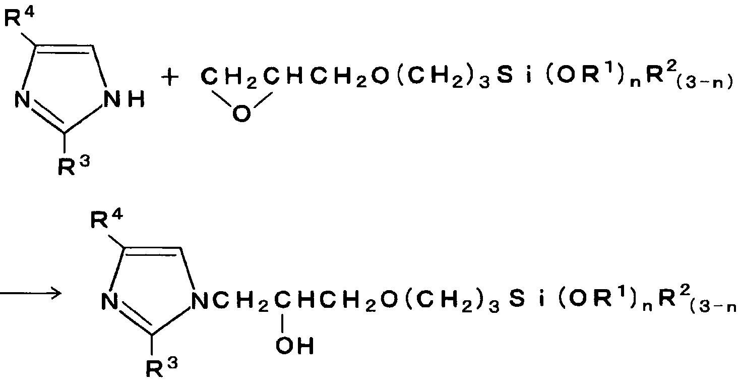
- Preferred examples include a silane-based printing agent obtained by a reaction between an azole compound and an epoxysilane compound.
- particularly preferred silane coupling agents include those obtained by reacting an imidazole compound as an azole compound.
- Epoxysilane compounds to be reacted with such a nitrogen-containing heterocyclic azole compound include H 20 (CH2) 3 Si (OR 1 ) nR 2 on)
- R ′ and R 2 are hydrogen or an alkyl group having 1 to 3 carbon atoms, and n is 0 to 3).
- the reaction between the azole compound and the epoxy group-containing silane compound can be performed under the conditions described in JP-A-6-256358. For example, at 80 to 200 ° C., 0.1 to 10 mol of an epoxy group-containing silane compound is added dropwise to 1 mol of the azole compound, and the mixture is reacted for 5 minutes to 2 hours. At this time, no solvent is required, but using an organic solvent such as chloroform, dioxanemethanol, or ethanol. Is also good.
- reaction between the imidazole compound and the epoxysilane-based compound shown as the particularly preferred example is as follows.
- RR 2 is hydrogen or an alkyl group having 1 to 3 carbon atoms
- R 3 is hydrogen or an alkyl group having 1 to 20 carbon atoms
- R 4 is a vinyl group, or an alkyl group having 1 to 5 carbon atoms.
- N represents 0 to 3
- silane coupling agent having a metal-capturing ability examples include: aminoaminopropyltrimethoxysilane, aminopropyltriethoxysilane, N-? (Aminoethyl) amino.
- aminoaminopropyltrimethoxysilane aminopropyltriethoxysilane
- aminopropyltriethoxysilane N-? (Aminoethyl) amino.
- the palladium compound chloride, hydroxide, oxide, sulfate, ammonium, and the like of palladium exhibiting a catalytic effect at the time of depositing copper, nickel, cobalt, and the like from the electroless plating solution on the surface of the adherend.
- Examples thereof include ammine complexes such as salts, and palladium chloride is particularly preferable.
- the palladium compound must be used as an organic solvent solution. Examples of the organic solvent include methyl alcohol and ethyl alcohol.
- Alcohol isopropanol, acetone, methyl ethyl ketone, toluene, ethylene glycol, polyethylene glycol, dimethylformamide, dimethyl sulfoxide, dioxane, and the like, and mixtures thereof.
- concentration in the solution is preferably 20 to 30 O mg / L.
- the semiconductor wafer referred to in the present invention includes not only a silicon-based wafer but also a compound semiconductor-based wafer such as gallium arsenide, gallium-phosphorus, and indium-phosphorus.
- the material of the surface to be covered of the semiconductor wafer is not limited.
- the barrier metal is the surface to be covered, and in any case, the method of the present invention can be preferably applied.
- the method of the present invention can also be preferably applied when the surface to be covered is silicon or its oxide film.
- this solution may be a suitable solvent such as water, methyl alcohol, ethyl alcohol, or isopropanol. It can be used in solutions such as acetone, methylethyl ketone, toluene, ethylene glycol, polyethylene glycol, dimethylformamide, dimethylsulfoxide, dioxane and the like or a mixture thereof.
- water it is necessary to optimize the pH of the solution, especially according to the surface to be coated and the plating conditions.
- the concentration of the silane coupling agent having a functional group having a metal-capturing ability in the solution is not limited to this, but is preferably 0.01 to 10% by weight. If the content is less than 0.001% by weight, the amount of the compound adhering to the surface of the substrate tends to be low, and the effect is hardly obtained. On the other hand, if the content exceeds 10% by weight, the amount of adhesion is so large that it is difficult to dry and that the powder is apt to agglomerate.
- the drying step can be omitted, and plating can be performed only by washing with water after surface treatment. However, at this time, it is necessary to perform sufficient washing with water to prevent the catalyst from being brought into the plating solution. Room temperature is sufficient for pretreatment, but heating can increase the deposition rate and amount of catalyst. The heating temperature is
- the covering surface may be cleaned before performing the plating pretreatment. Before plating, it may be effective to treat with a solution containing a reducing agent. Particularly in the case of copper plating, treatment with a dimethylamine-borane solution or the like as a reducing agent is preferable.
- metals such as copper, nickel, cobalt, tin, and gold can be plated on a semiconductor wafer by electroless plating.
- a via-trench is formed on the surface of a semiconductor (such as silicon) wafer to embed copper wiring, and titanium is formed on the surface to prevent copper from diffusing into silicon.
- a barrier metal selected from the group consisting of tungsten, tantalum, tungsten or a nitride thereof (nitride) is coated to a thickness of about 0.01 to 0.1 / m by sputtering, CVD, or the like.
- a thin copper layer is coated on the barrier metal layer by sputtering, CVD, or the like in the same manner as described above.
- the barrier metal is generally Since the electrical resistance is large, and the difference in current density between the periphery and the center located at the periphery of the wafer is large when the copper is coated later, copper with a small electrical resistance is applied in advance. Coating).
- the conventional inner ring method cannot provide sufficient coverage of the inner wall of the via / trench. Defects (boad seam) may occur.
- the CVD method has the problem that the coverage is improved but the cost is extremely high.
- the seed layer is formed by electrolessly depositing copper or nickel after applying a catalyst on the barrier metal by the pretreatment method, instead of the conventional seed layer film forming method.
- This method can solve the problem of insufficient power barrier on the inner wall of vias and trenches in the case of fine wiring at a lower cost than the CVD method.
- copper is electrolessly deposited, it is possible to continually embed the wiring without electrolysis, instead of using it as a seed layer.
- electroless plating if the catalyst is uniformly deposited on the surface to be plated, the film grows evenly on the surface to be covered, so that in the case of fine wiring, a seam tends to occur.
- the catalyst when the catalyst is applied by the pretreatment method, the catalyst tends to adhere to the inner wall of the fine wiring. Metals tend to be deposited more easily in places where the amount of catalyst attached is large.Therefore, depending on the aspect ratio of vias and trenches, bottom-up precipitation such as electrolytic copper plating liquid used for embedding fine wiring may occur. As a result, it becomes possible to bury fine wiring without generating seams.
- the electroless copper plating solution contains formalin as a reducing agent. However, the use of formalin tends to be avoided in recent years due to the growing problem of environmental impact.
- electroless nickel plating solution Since it contains several percent of phosphorus or boron, the electrical resistance increases. Therefore, when the seed layer is formed by electroless nickel plating, it is necessary to suppress the film thickness to a minimum value that allows conduction.
- the electroless copper plating solution and the electroless nickel plating solution often contain an alkali component as a raw material. Alkali components are the most disliked impurities in wiring materials, so raw materials that do not contain these must be used. For example, it is preferable to use tetramethylammonium hydroxide instead of sodium hydroxide used for pH adjustment. Also, dimethylamine-borane is preferably used as a reducing agent in the electroless nickel plating solution.
- barrier metal can be formed on an insulating film.
- barrier metals in this case would be nickel, cobalt or alloys of these metals with other metals (such as tungsten).
- the film thickness is 7 OA or more and 500 OA or less
- the average surface roughness Ra is 100 A or more and 100 A or less
- the film thickness is 100 A or more and 300 000 or less.
- a or less, average surface roughness Ra A plating layer of 2 OA or more and 70 A or less can be formed o
- a 0.2% isopropyl alcohol solution of a silane coupling agent which is an equimolar reaction product of imidazole and ⁇ -glycidoxypropyltrimethoxysilane, was spin-coated on a silicon wafer whose surface was made Si 0 2 by thermal diffusion. The coating was performed overnight at 100 rpm for 1 minute. After drying at 100 ° C for 5 minutes with a drier, cool to room temperature, and apply an isopropyl alcohol solution of palladium chloride (Pd concentration 6 O mg / L) at 100 rpm for 1 minute by spinco overnight. Apply under conditions did.
- a silane coupling agent which is an equimolar reaction product of imidazole and ⁇ -glycidoxypropyltrimethoxysilane
- Pd concentration 6 Omg / L
- the 0.022% methyl E chill ketone solution of a silane force Dzupuringu agent is an equimolar reaction product of the surface and the S i 0 to silicone wafers one you 2 Imidazo Ichiru and y- glycidoxypropyltrimethoxysilane main Tokishishiran by CVD
- the coating was performed at 1,000 rpm for 1 minute by spinco overnight. After drying with a dryer at 100 ° C for 5 minutes, After cooling to room temperature, a solution of palladium chloride in methyl ethyl ketone (? (1 concentration: 60111 / L)) was applied by a spinco overnight at 1000 rpm for 1 minute, and dried at 100 ° C for 5 minutes.
- Pd concentration 10 Omg / L
- Isopropyl alcohol was applied to a silicon wafer having a surface of Sio 2 at 1000 rpm for 1 minute by spinning overnight. After drying at 100 ° C for 5 minutes with a drier, the solution was cooled to room temperature, and an aqueous solution of palladium chloride (Pd concentration 60 mg / L) was applied at 1,000 rpm for 1 minute by a spinco overnight. After drying at 100 ° C for 5 minutes using a drier, it was cooled to room temperature, immersed in an electroless nickel plating solution, and electroless nickel plating was performed. No attachment was found on the wafer.
- a solution of palladium chloride in isopropyl alcohol (Pd concentration: 6 Omg / L) was applied to the silicon wafer having a surface of Sio 2 at 1000 rpm for 1 minute by a spinco overnight. After drying at 100 ° C for 5 minutes using a drier, it was cooled to room temperature, immersed in an electroless nickel plating solution, and electroless nickel plating was performed. No plating was found on the wafer.
- the vias and trenches formed on the surface are also used.
- a palladium compound as a catalyst as an organic solvent solution on the wall surface, it can be fixed uniformly, facilitating electroless plating. enable.
- a metal thin film which is also suitable as a seed layer on a semiconductor wafer can be formed with good adhesion, uniformly and smoothly.
Landscapes
- Chemical & Material Sciences (AREA)
- General Chemical & Material Sciences (AREA)
- Chemical Kinetics & Catalysis (AREA)
- Engineering & Computer Science (AREA)
- Materials Engineering (AREA)
- Mechanical Engineering (AREA)
- Metallurgy (AREA)
- Organic Chemistry (AREA)
- Inorganic Chemistry (AREA)
- Chemically Coating (AREA)
- Electrodes Of Semiconductors (AREA)
Description

Claims
Priority Applications (4)
| Application Number | Priority Date | Filing Date | Title |
|---|---|---|---|
| EP03747201.6A EP1498511B1 (en) | 2002-04-23 | 2003-03-26 | Method of electroless plating and semiconductor wafer having metal plating layer formed thereon |
| US10/472,678 US7179741B2 (en) | 2002-04-23 | 2003-03-26 | Electroless plating method and semiconductor wafer on which metal plating layer is formed |
| KR1020037011990A KR100560268B1 (ko) | 2002-04-23 | 2003-03-26 | 무전해 도금방법 및 금속도금층이 형성된 반도체 웨이퍼 |
| JP2003587998A JPWO2003091476A1 (ja) | 2002-04-23 | 2003-03-26 | 無電解めっき方法及び金属めっき層が形成された半導体ウエハー |
Applications Claiming Priority (2)
| Application Number | Priority Date | Filing Date | Title |
|---|---|---|---|
| JP2002120289 | 2002-04-23 | ||
| JP2002-120289 | 2002-04-23 |
Publications (1)
| Publication Number | Publication Date |
|---|---|
| WO2003091476A1 true WO2003091476A1 (en) | 2003-11-06 |
Family
ID=29267364
Family Applications (1)
| Application Number | Title | Priority Date | Filing Date |
|---|---|---|---|
| PCT/JP2003/003707 Ceased WO2003091476A1 (en) | 2002-04-23 | 2003-03-26 | Method of electroless plating and semiconductor wafer having metal plating layer formed thereon |
Country Status (7)
| Country | Link |
|---|---|
| US (1) | US7179741B2 (ja) |
| EP (1) | EP1498511B1 (ja) |
| JP (1) | JPWO2003091476A1 (ja) |
| KR (1) | KR100560268B1 (ja) |
| CN (1) | CN100348775C (ja) |
| TW (1) | TWI236070B (ja) |
| WO (1) | WO2003091476A1 (ja) |
Cited By (10)
| Publication number | Priority date | Publication date | Assignee | Title |
|---|---|---|---|---|
| WO2006027947A1 (ja) * | 2004-09-10 | 2006-03-16 | Nippon Mining & Metals Co., Ltd. | 無電解めっき前処理剤及びフレキシブル基板用銅張り積層体 |
| WO2006134899A1 (ja) * | 2005-06-13 | 2006-12-21 | Tohoku University | 薄膜トランジスタ、配線板、及び電子装置の製造方法 |
| KR100796894B1 (ko) * | 2004-01-29 | 2008-01-22 | 닛코킨조쿠 가부시키가이샤 | 무전해 도금 전처리제, 그것을 이용하는 무전해 도금방법,및 무전해 도금물 |
| JP2008069389A (ja) * | 2006-09-13 | 2008-03-27 | Univ Waseda | 積層構造、超lsi配線板及びそれらの形成方法 |
| JP2008166341A (ja) * | 2006-12-27 | 2008-07-17 | Casio Comput Co Ltd | 半導体装置およびその製造方法 |
| WO2009084470A1 (ja) * | 2007-12-27 | 2009-07-09 | Fujifilm Corporation | めっき方法、金属薄膜形成方法、及びめっき触媒液 |
| JP2009246212A (ja) * | 2008-03-31 | 2009-10-22 | Dainippon Printing Co Ltd | 導電性基板の製造方法及び導電性基板 |
| US8404035B2 (en) | 2003-10-17 | 2013-03-26 | Nippon Mining & Metals Co., Ltd. | Electroless copper plating solution |
| JP2016183388A (ja) * | 2015-03-26 | 2016-10-20 | 東京エレクトロン株式会社 | 密着層形成方法、密着層形成システムおよび記憶媒体 |
| JP2019529710A (ja) * | 2016-09-16 | 2019-10-17 | アトテック ドイチェランド ゲーエムベーハー | 基板の表面に多層コーティングを提供するための方法 |
Families Citing this family (20)
| Publication number | Priority date | Publication date | Assignee | Title |
|---|---|---|---|---|
| WO2004108986A1 (ja) * | 2003-06-09 | 2004-12-16 | Nikko Materials Co., Ltd. | 無電解めっき方法及び金属めっき物 |
| EP1681321B1 (en) * | 2003-11-05 | 2011-08-10 | Nippon Mining & Metals Co., Ltd. | Inkjet ink composition |
| BRPI0511354A (pt) * | 2004-06-25 | 2007-12-04 | Nippon Mining Co | agente de tratamento de superfìcie metálica para promover a adesão borracha-metal |
| US7709873B2 (en) * | 2005-03-31 | 2010-05-04 | Intel Corporation | Polymer memory with adhesion layer containing an immobilized metal |
| US20070004587A1 (en) * | 2005-06-30 | 2007-01-04 | Intel Corporation | Method of forming metal on a substrate using a Ruthenium-based catalyst |
| US20070080067A1 (en) * | 2005-10-07 | 2007-04-12 | Applied Materials, Inc. | Pre-treatment to eliminate the defects formed during electrochemical plating |
| US7629252B2 (en) * | 2005-12-23 | 2009-12-08 | Intel Corporation | Conformal electroless deposition of barrier layer materials |
| US20070235876A1 (en) * | 2006-03-30 | 2007-10-11 | Michael Goldstein | Method of forming an atomic layer thin film out of the liquid phase |
| US20080003366A1 (en) * | 2006-06-30 | 2008-01-03 | Dubin Valery M | Method of forming a conducting layer on a conducting and non-conducting substrate |
| US20080160177A1 (en) * | 2006-12-29 | 2008-07-03 | Mataybas J C | Methods for electroless plating of metal traces on a substrate and devices and systems thereof |
| US20090162681A1 (en) * | 2007-12-21 | 2009-06-25 | Artur Kolics | Activation solution for electroless plating on dielectric layers |
| JP2009174041A (ja) * | 2007-12-27 | 2009-08-06 | Fujifilm Corp | めっき触媒吸着方法、金属層付き基板の製造方法及びそれらに用いるめっき触媒液 |
| US8377840B2 (en) * | 2009-02-13 | 2013-02-19 | Babcock & Wilcox Technical Services Y-12, Llc | Method of producing catalytic materials for fabricating nanostructures |
| KR101445461B1 (ko) * | 2010-03-23 | 2014-09-26 | 제이엑스 닛코 닛세키 킨조쿠 가부시키가이샤 | 무전해 도금 전처리제, 그것을 이용하는 무전해 도금 방법 및 무전해 도금물 |
| US8895441B2 (en) | 2012-02-24 | 2014-11-25 | Lam Research Corporation | Methods and materials for anchoring gapfill metals |
| US20170073815A1 (en) * | 2015-09-10 | 2017-03-16 | Lam Research Corporation | Method for a non-aqueous electroless polyol deposition of metal or metal alloy in features of a substrate |
| US11152294B2 (en) | 2018-04-09 | 2021-10-19 | Corning Incorporated | Hermetic metallized via with improved reliability |
| US12200875B2 (en) | 2018-09-20 | 2025-01-14 | Industrial Technology Research Institute | Copper metallization for through-glass vias on thin glass |
| EP3880865A2 (en) * | 2018-11-13 | 2021-09-22 | Corning Incorporated | 3d interposer with through glas vias-method of increasing adhesion between copper and class surfaces and articles therefrom |
| US11760682B2 (en) | 2019-02-21 | 2023-09-19 | Corning Incorporated | Glass or glass ceramic articles with copper-metallized through holes and processes for making the same |
Citations (3)
| Publication number | Priority date | Publication date | Assignee | Title |
|---|---|---|---|---|
| EP0347114A1 (en) * | 1988-06-11 | 1989-12-20 | Nisshinbo Industries, Inc. | Metallic colloidal dispersions |
| JP2001181853A (ja) * | 1999-12-28 | 2001-07-03 | Nisshinbo Ind Inc | 非水系無電解めっき液及び該めっき液を用いためっき方法 |
| US20020036143A1 (en) * | 2000-04-10 | 2002-03-28 | Yuji Segawa | Method of electroless plating and electroless plating apparatus |
Family Cites Families (17)
| Publication number | Priority date | Publication date | Assignee | Title |
|---|---|---|---|---|
| US3963841A (en) | 1975-01-06 | 1976-06-15 | International Business Machines Corporation | Catalytic surface preparation for electroless plating |
| US5077085A (en) | 1987-03-06 | 1991-12-31 | Schnur Joel M | High resolution metal patterning of ultra-thin films on solid substrates |
| BE1007879A3 (fr) * | 1994-01-05 | 1995-11-07 | Blue Chips Holding | Resine polymerique a viscosite ajustable pour le depot de palladium catalytique sur un substrat, son procede de preparation et son utilisation. |
| JPH11510219A (ja) | 1995-12-19 | 1999-09-07 | エフエスアイ インターナショナル インコーポレイテッド | スプレー・プロセッサを用いる金属膜の無電解めっき |
| JP3533935B2 (ja) * | 1997-03-26 | 2004-06-07 | 信越化学工業株式会社 | 回路基板の製造方法 |
| JP3368799B2 (ja) * | 1997-05-22 | 2003-01-20 | 住友電気工業株式会社 | Iii−v族化合物半導体ウェハおよびその製造方法 |
| US6284309B1 (en) * | 1997-12-19 | 2001-09-04 | Atotech Deutschland Gmbh | Method of producing copper surfaces for improved bonding, compositions used therein and articles made therefrom |
| JP3539234B2 (ja) | 1998-10-22 | 2004-07-07 | 信越化学工業株式会社 | 金属パターン用被膜形成用ポリシラン組成物及び金属パターン形成方法 |
| US6344309B2 (en) * | 1998-10-22 | 2002-02-05 | Shin-Etsu Chemical Co., Ltd. | Polysilane composition for forming a coating suitable for bearing a metal pattern, metal pattern forming method, wiring board preparing method |
| JP2000349417A (ja) | 1999-06-02 | 2000-12-15 | Shin Etsu Chem Co Ltd | 配線基板の製造方法 |
| CN1174118C (zh) * | 2000-01-07 | 2004-11-03 | 株式会社日矿材料 | 金属镀覆方法、预处理剂以及使用它们制得的半导体晶片和半导体器件 |
| JP2001230527A (ja) * | 2000-02-14 | 2001-08-24 | Seiko Epson Corp | 導電膜パターン形成方法、及び導電膜パターン |
| WO2001081652A1 (en) | 2000-04-25 | 2001-11-01 | Nikko Materials Co., Ltd. | Pretreating agent for metal plating |
| JP2001323381A (ja) | 2000-05-16 | 2001-11-22 | Sony Corp | めっき方法及びめっき構造 |
| TWI230187B (en) * | 2000-11-02 | 2005-04-01 | Shipley Co Llc | Process for treating adhesion promoted metal surfaces with an organo-silicon post-treatment |
| KR20030085569A (ko) * | 2001-03-26 | 2003-11-05 | 닛뽕 뻬인또 가부시키가이샤 | 금속 패턴의 형성 방법 |
| US6767828B2 (en) * | 2001-10-05 | 2004-07-27 | International Business Machines Corporation | Method for forming patterns for semiconductor devices |
-
2003
- 2003-03-26 JP JP2003587998A patent/JPWO2003091476A1/ja active Pending
- 2003-03-26 KR KR1020037011990A patent/KR100560268B1/ko not_active Expired - Lifetime
- 2003-03-26 CN CNB038001721A patent/CN100348775C/zh not_active Expired - Lifetime
- 2003-03-26 WO PCT/JP2003/003707 patent/WO2003091476A1/ja not_active Ceased
- 2003-03-26 EP EP03747201.6A patent/EP1498511B1/en not_active Expired - Lifetime
- 2003-03-26 US US10/472,678 patent/US7179741B2/en not_active Expired - Lifetime
- 2003-04-16 TW TW092108775A patent/TWI236070B/zh not_active IP Right Cessation
Patent Citations (3)
| Publication number | Priority date | Publication date | Assignee | Title |
|---|---|---|---|---|
| EP0347114A1 (en) * | 1988-06-11 | 1989-12-20 | Nisshinbo Industries, Inc. | Metallic colloidal dispersions |
| JP2001181853A (ja) * | 1999-12-28 | 2001-07-03 | Nisshinbo Ind Inc | 非水系無電解めっき液及び該めっき液を用いためっき方法 |
| US20020036143A1 (en) * | 2000-04-10 | 2002-03-28 | Yuji Segawa | Method of electroless plating and electroless plating apparatus |
Cited By (11)
| Publication number | Priority date | Publication date | Assignee | Title |
|---|---|---|---|---|
| US8404035B2 (en) | 2003-10-17 | 2013-03-26 | Nippon Mining & Metals Co., Ltd. | Electroless copper plating solution |
| KR100796894B1 (ko) * | 2004-01-29 | 2008-01-22 | 닛코킨조쿠 가부시키가이샤 | 무전해 도금 전처리제, 그것을 이용하는 무전해 도금방법,및 무전해 도금물 |
| WO2006027947A1 (ja) * | 2004-09-10 | 2006-03-16 | Nippon Mining & Metals Co., Ltd. | 無電解めっき前処理剤及びフレキシブル基板用銅張り積層体 |
| WO2006134899A1 (ja) * | 2005-06-13 | 2006-12-21 | Tohoku University | 薄膜トランジスタ、配線板、及び電子装置の製造方法 |
| JP2008069389A (ja) * | 2006-09-13 | 2008-03-27 | Univ Waseda | 積層構造、超lsi配線板及びそれらの形成方法 |
| JP2008166341A (ja) * | 2006-12-27 | 2008-07-17 | Casio Comput Co Ltd | 半導体装置およびその製造方法 |
| WO2009084470A1 (ja) * | 2007-12-27 | 2009-07-09 | Fujifilm Corporation | めっき方法、金属薄膜形成方法、及びめっき触媒液 |
| JP2009246212A (ja) * | 2008-03-31 | 2009-10-22 | Dainippon Printing Co Ltd | 導電性基板の製造方法及び導電性基板 |
| JP2016183388A (ja) * | 2015-03-26 | 2016-10-20 | 東京エレクトロン株式会社 | 密着層形成方法、密着層形成システムおよび記憶媒体 |
| US10354915B2 (en) | 2015-03-26 | 2019-07-16 | Tokyo Electron Limited | Adhesion layer forming method, adhesion layer forming system and recording medium |
| JP2019529710A (ja) * | 2016-09-16 | 2019-10-17 | アトテック ドイチェランド ゲーエムベーハー | 基板の表面に多層コーティングを提供するための方法 |
Also Published As
| Publication number | Publication date |
|---|---|
| EP1498511B1 (en) | 2016-07-06 |
| EP1498511A4 (en) | 2006-10-11 |
| KR100560268B1 (ko) | 2006-03-10 |
| TW200400567A (en) | 2004-01-01 |
| JPWO2003091476A1 (ja) | 2005-09-02 |
| KR20040004556A (ko) | 2004-01-13 |
| TWI236070B (en) | 2005-07-11 |
| CN100348775C (zh) | 2007-11-14 |
| US7179741B2 (en) | 2007-02-20 |
| CN1623009A (zh) | 2005-06-01 |
| US20040235294A1 (en) | 2004-11-25 |
| EP1498511A1 (en) | 2005-01-19 |
Similar Documents
| Publication | Publication Date | Title |
|---|---|---|
| KR100560268B1 (ko) | 무전해 도금방법 및 금속도금층이 형성된 반도체 웨이퍼 | |
| JP3670238B2 (ja) | 金属めっき方法、前処理剤、それを用いた半導体ウェハー及び半導体装置 | |
| US6780467B2 (en) | Plating pretreatment agent and metal plating method using the same | |
| US7867564B2 (en) | Metal plating method and pretreatment agent | |
| JPWO2001049898A1 (ja) | 金属めっき方法、前処理剤、それを用いた半導体ウェハー及び半導体装置 | |
| CN1910305B (zh) | 化学镀预处理剂、利用它的化学镀方法和化学镀产品 | |
| JP3654354B2 (ja) | 超lsi配線板及びその製造方法 | |
| US7045461B2 (en) | Metal plating method, pretreatment agent, and semiconductor wafer and semiconductor device obtained using these | |
| CN100462480C (zh) | 无电镀铜溶液 | |
| JP3277463B2 (ja) | 金属めっき前処理剤、およびそれを用いる金属めっき方法 | |
| US8182873B2 (en) | Method for electroless plating and metal-plated article | |
| JP2003313669A (ja) | 無電解めっき方法およびそれにより金属めっき層が形成された半導体ウエハー | |
| JP2005213576A (ja) | 無電解めっき前処理剤、それを用いる無電解めっき方法、及び無電解めっき物 | |
| CN101292343B (zh) | 在双镶嵌互连上的覆盖层的形成 | |
| JP2003193245A (ja) | めっき前処理剤、及びそれを用いた無電解めっき方法 | |
| JP4425453B2 (ja) | 金属膜間密着性向上方法 | |
| KR20080048043A (ko) | 스루홀을 가진 프린트 배선 기판에의 무전해 도금용 촉매,및 그 촉매를 이용하여 처리된 스루홀을 가진 프린트 배선기판 | |
| JP2003041374A (ja) | 表面処理剤、およびそれを用いた表面処理物 | |
| HK40099233A (zh) | 用於扩散阻挡层形成的方法和湿式化学组成 | |
| US20040265600A1 (en) | Material for forming copper undercoat films |
Legal Events
| Date | Code | Title | Description |
|---|---|---|---|
| WWE | Wipo information: entry into national phase |
Ref document number: 2003587998 Country of ref document: JP |
|
| WWE | Wipo information: entry into national phase |
Ref document number: 1020037011990 Country of ref document: KR |
|
| WWE | Wipo information: entry into national phase |
Ref document number: 10472678 Country of ref document: US |
|
| REEP | Request for entry into the european phase |
Ref document number: 2003747201 Country of ref document: EP |
|
| WWE | Wipo information: entry into national phase |
Ref document number: 2003747201 Country of ref document: EP |
|
| WWE | Wipo information: entry into national phase |
Ref document number: 038001721 Country of ref document: CN |
|
| AK | Designated states |
Kind code of ref document: A1 Designated state(s): CN JP KR US |
|
| AL | Designated countries for regional patents |
Kind code of ref document: A1 Designated state(s): DE FR GB IT |
|
| 121 | Ep: the epo has been informed by wipo that ep was designated in this application | ||
| WWP | Wipo information: published in national office |
Ref document number: 2003747201 Country of ref document: EP |