WO2004067666A1 - 接着シートおよび積層体 - Google Patents
接着シートおよび積層体 Download PDFInfo
- Publication number
- WO2004067666A1 WO2004067666A1 PCT/JP2004/000757 JP2004000757W WO2004067666A1 WO 2004067666 A1 WO2004067666 A1 WO 2004067666A1 JP 2004000757 W JP2004000757 W JP 2004000757W WO 2004067666 A1 WO2004067666 A1 WO 2004067666A1
- Authority
- WO
- WIPO (PCT)
- Prior art keywords
- layer
- laminate
- wholly aromatic
- adhesive sheet
- substrate
- Prior art date
- Legal status (The legal status is an assumption and is not a legal conclusion. Google has not performed a legal analysis and makes no representation as to the accuracy of the status listed.)
- Ceased
Links
Classifications
-
- H—ELECTRICITY
- H10—SEMICONDUCTOR DEVICES; ELECTRIC SOLID-STATE DEVICES NOT OTHERWISE PROVIDED FOR
- H10P—GENERIC PROCESSES OR APPARATUS FOR THE MANUFACTURE OR TREATMENT OF DEVICES COVERED BY CLASS H10
- H10P90/00—Preparation of wafers not covered by a single main group of this subclass, e.g. wafer reinforcement
- H10P90/19—Preparing inhomogeneous wafers
- H10P90/1904—Preparing vertically inhomogeneous wafers
- H10P90/1906—Preparing SOI wafers
- H10P90/1914—Preparing SOI wafers using bonding
-
- C—CHEMISTRY; METALLURGY
- C09—DYES; PAINTS; POLISHES; NATURAL RESINS; ADHESIVES; COMPOSITIONS NOT OTHERWISE PROVIDED FOR; APPLICATIONS OF MATERIALS NOT OTHERWISE PROVIDED FOR
- C09J—ADHESIVES; NON-MECHANICAL ASPECTS OF ADHESIVE PROCESSES IN GENERAL; ADHESIVE PROCESSES NOT PROVIDED FOR ELSEWHERE; USE OF MATERIALS AS ADHESIVES
- C09J7/00—Adhesives in the form of films or foils
- C09J7/20—Adhesives in the form of films or foils characterised by their carriers
- C09J7/22—Plastics; Metallised plastics
-
- C—CHEMISTRY; METALLURGY
- C09—DYES; PAINTS; POLISHES; NATURAL RESINS; ADHESIVES; COMPOSITIONS NOT OTHERWISE PROVIDED FOR; APPLICATIONS OF MATERIALS NOT OTHERWISE PROVIDED FOR
- C09J—ADHESIVES; NON-MECHANICAL ASPECTS OF ADHESIVE PROCESSES IN GENERAL; ADHESIVE PROCESSES NOT PROVIDED FOR ELSEWHERE; USE OF MATERIALS AS ADHESIVES
- C09J7/00—Adhesives in the form of films or foils
- C09J7/30—Adhesives in the form of films or foils characterised by the adhesive composition
- C09J7/35—Heat-activated
-
- C—CHEMISTRY; METALLURGY
- C09—DYES; PAINTS; POLISHES; NATURAL RESINS; ADHESIVES; COMPOSITIONS NOT OTHERWISE PROVIDED FOR; APPLICATIONS OF MATERIALS NOT OTHERWISE PROVIDED FOR
- C09J—ADHESIVES; NON-MECHANICAL ASPECTS OF ADHESIVE PROCESSES IN GENERAL; ADHESIVE PROCESSES NOT PROVIDED FOR ELSEWHERE; USE OF MATERIALS AS ADHESIVES
- C09J2301/00—Additional features of adhesives in the form of films or foils
-
- C—CHEMISTRY; METALLURGY
- C09—DYES; PAINTS; POLISHES; NATURAL RESINS; ADHESIVES; COMPOSITIONS NOT OTHERWISE PROVIDED FOR; APPLICATIONS OF MATERIALS NOT OTHERWISE PROVIDED FOR
- C09J—ADHESIVES; NON-MECHANICAL ASPECTS OF ADHESIVE PROCESSES IN GENERAL; ADHESIVE PROCESSES NOT PROVIDED FOR ELSEWHERE; USE OF MATERIALS AS ADHESIVES
- C09J2477/00—Presence of polyamide
-
- C—CHEMISTRY; METALLURGY
- C09—DYES; PAINTS; POLISHES; NATURAL RESINS; ADHESIVES; COMPOSITIONS NOT OTHERWISE PROVIDED FOR; APPLICATIONS OF MATERIALS NOT OTHERWISE PROVIDED FOR
- C09J—ADHESIVES; NON-MECHANICAL ASPECTS OF ADHESIVE PROCESSES IN GENERAL; ADHESIVE PROCESSES NOT PROVIDED FOR ELSEWHERE; USE OF MATERIALS AS ADHESIVES
- C09J2479/00—Presence of polyamine or polyimide
- C09J2479/08—Presence of polyamine or polyimide polyimide
- C09J2479/086—Presence of polyamine or polyimide polyimide in the substrate
-
- H—ELECTRICITY
- H10—SEMICONDUCTOR DEVICES; ELECTRIC SOLID-STATE DEVICES NOT OTHERWISE PROVIDED FOR
- H10W—GENERIC PACKAGES, INTERCONNECTIONS, CONNECTORS OR OTHER CONSTRUCTIONAL DETAILS OF DEVICES COVERED BY CLASS H10
- H10W10/00—Isolation regions in semiconductor bodies between components of integrated devices
- H10W10/10—Isolation regions comprising dielectric materials
- H10W10/181—Semiconductor-on-insulator [SOI] isolation regions, e.g. buried oxide regions of SOI wafers
-
- Y—GENERAL TAGGING OF NEW TECHNOLOGICAL DEVELOPMENTS; GENERAL TAGGING OF CROSS-SECTIONAL TECHNOLOGIES SPANNING OVER SEVERAL SECTIONS OF THE IPC; TECHNICAL SUBJECTS COVERED BY FORMER USPC CROSS-REFERENCE ART COLLECTIONS [XRACs] AND DIGESTS
- Y10—TECHNICAL SUBJECTS COVERED BY FORMER USPC
- Y10T—TECHNICAL SUBJECTS COVERED BY FORMER US CLASSIFICATION
- Y10T428/00—Stock material or miscellaneous articles
- Y10T428/28—Web or sheet containing structurally defined element or component and having an adhesive outermost layer
-
- Y—GENERAL TAGGING OF NEW TECHNOLOGICAL DEVELOPMENTS; GENERAL TAGGING OF CROSS-SECTIONAL TECHNOLOGIES SPANNING OVER SEVERAL SECTIONS OF THE IPC; TECHNICAL SUBJECTS COVERED BY FORMER USPC CROSS-REFERENCE ART COLLECTIONS [XRACs] AND DIGESTS
- Y10—TECHNICAL SUBJECTS COVERED BY FORMER USPC
- Y10T—TECHNICAL SUBJECTS COVERED BY FORMER US CLASSIFICATION
- Y10T428/00—Stock material or miscellaneous articles
- Y10T428/28—Web or sheet containing structurally defined element or component and having an adhesive outermost layer
- Y10T428/2852—Adhesive compositions
-
- Y—GENERAL TAGGING OF NEW TECHNOLOGICAL DEVELOPMENTS; GENERAL TAGGING OF CROSS-SECTIONAL TECHNOLOGIES SPANNING OVER SEVERAL SECTIONS OF THE IPC; TECHNICAL SUBJECTS COVERED BY FORMER USPC CROSS-REFERENCE ART COLLECTIONS [XRACs] AND DIGESTS
- Y10—TECHNICAL SUBJECTS COVERED BY FORMER USPC
- Y10T—TECHNICAL SUBJECTS COVERED BY FORMER US CLASSIFICATION
- Y10T428/00—Stock material or miscellaneous articles
- Y10T428/31504—Composite [nonstructural laminate]
- Y10T428/31721—Of polyimide
Definitions
- the present invention relates to an adhesive sheet, a laminate, and a method for producing the same.
- Conventional technology
- the manufacturing process for semiconductor devices such as silicon and gallium arsenide consists of a pre-process for forming devices in large-diameter semiconductors, and a post-process for separating the wafer into individual device pieces (chips) and finishing it into the final product. Divided.
- the pre-process as a method for reducing the size and thickness of the semiconductor chip, for example, after forming elements in a state of a large-diameter semiconductor wafer, a back grinding process such as grinding of the semiconductor wafer is performed, and the semiconductor wafer itself is cut. By reducing the thickness of the chip, the overall chip thickness is reduced.
- the side opposite to the surface to be ground of the semiconductor wafer must be bonded and fixed to a support via an adhesive sheet.
- a temperature of 400 ° C. or more is required. There has been a demand for an adhesive sheet having heat resistance.
- the semiconductor wafer is cut and separated (diced) for each chip, followed by a die-bonding process of the chip on a lead frame.
- the semiconductor wafer is diced, washed, and dried in a state in which it is attached to the adhesive sheet in advance. After that, the steps of expanding the adhesive sheet (expanding) and peeling off the chip from the adhesive sheet (pickup) are performed. Added. Adhesive sheets used in the processes from the dicing process to the pick-up process for semiconductor wafers must maintain sufficient adhesive strength to the chips from the dicing process to the drying process. It is desired to have good releasability to the extent that the agent does not adhere. In order to satisfy the requirements of these post-processes, various adhesive sheets for attaching a semiconductor wafer have been proposed.
- an adhesive formed using a composition comprising a (meth) acrylate copolymer, an epoxy resin, a photopolymerizable low molecular compound, a heat-active latent epoxy resin curing agent, and a photopolymerization initiator.
- a pressure-sensitive adhesive tape comprising an adhesive layer and a base material (see JP-A-2-321181); a polymer support film having a surface substantially free of a release layer; and a conductive adhesive.
- a dicing film see Japanese Patent Publication No. 3-344853
- an adhesive layer for die bonding are provided on an overheated foaming adhesive layer provided on a supporting substrate.
- a method has been proposed in which the adhesive layer and the heat-foamable pressure-sensitive adhesive layer can be peeled off by overheating (see JP-A-3-2684345).
- the conventional adhesive sheet has the following problems.
- the conventional adhesive sheet does not have sufficient strength as a support, and the semiconductor wafer may be broken during a manufacturing process such as grinding and transporting the semiconductor wafer for thinning, resulting in a product yield. There was a problem in the point.
- the adhesive sheet must have sufficient adhesiveness in the holding and transporting steps in the grinding process performed during semiconductor wafer manufacturing, but the adhesive sheet must remain on the semiconductor wafer side before the dicing process of the semiconductor wafer It is required that it can be peeled off without any problems And the reuse of the support From the viewpoint, it is desirable that the peeling from the support is finally easy.
- Another object of the present invention is to provide a method for obtaining a laminate including a target layer to be treated by subjecting a laminate including the adhesive sheet to treatment and then peeling the laminate.
- the present invention provides an adhesive sheet comprising a substrate (A) made of a wholly aromatic polyimide film and a thermal adhesive layer (C) made of a wholly aromatic polyamide having a glass transition point of 200 ° C to 500 ° C.
- a substrate (A) made of a wholly aromatic polyimide film
- a thermal adhesive layer (C) made of a wholly aromatic polyamide having a glass transition point of 200 ° C to 500 ° C.
- the present invention is a laminate (I) in which the adhesive sheet is bonded to an inorganic material.
- the present invention also relates to a laminate (II) in which an organic protective layer (E) and an object layer (D) are laminated on the laminate (I), and a method for producing the laminate.
- the present invention also provides a laminate comprising a base material (A) made of a wholly aromatic polyimide film having a glass transition point of 200 ° C. or higher and an inorganic material (B), wherein the base material (A) When a substrate and a silicon wafer are laminated, the base material (A) becomes
- the peel strength at the interface between the base material (A) and the silicon wafer after thermocompression bonding at 370 ° C and 5.0 to 6.0 MPa for 15 minutes should be 0.1 lNZm to 100 NZm. This is a characteristic laminate ( ⁇ ).
- the present invention also relates to a laminate ( ⁇ ) in which an organic protective layer (E) and an object layer (D) are laminated on the laminate (1 ′), and a method for producing them.
- the exposed surface of the D layer is subjected to a thinning treatment to obtain a D layer, and a laminate comprising a D ′ layer, an E layer, an A layer, a C layer, and a B layer.
- a stacked body (IV) composed of the D 'layer and the E layer.
- substrate made of a wholly aromatic polyimide film (A) Oyopiga glass transition point of 200 ° C ⁇ 50 O p
- thermal adhesive layers (C) made of wholly aromatic polyamides having the properties of C and adhesive sheets made of such.
- the adhesive sheet of the present invention preferably has a Young's modulus in the range of 1.0 GPa to 30 GPa. If the Young's modulus is less than 1.0 GPa, handling properties will be poor, and if it is higher than 30 GPa, it will be difficult for the adhesive sheet itself to relieve the residual stress generated during cooling after thermocompression bonding due to the difference in thermal expansion. However, the adhesive strength may be significantly reduced. Preferably, it is in the range of 2. OGPa to 25 GPa. More preferably, it is in the range of 3.0 GPa to 20 GPa, and more preferably 10.0 GPa to 20 GPa.
- the Young's modulus used here is measured at a stretching rate of 5 mmZ for a single bow using a sample of 5 OmmX 1 Omm, and the elongation is 100% from the initial slope of the elongation-strength curve of the obtained data. It is a value calculated by converting the strength at the time of performing.
- the adhesive sheet has a linear thermal expansion coefficient of -10 pp mZ. It is preferably in the range of +45 pp mZ ° C. In a preferred embodiment of the present invention, it is used as an adherend
- the linear thermal expansion coefficient of the inorganic material ranges from 1-5 ppmZ ° C to +35 ppmZt. For this reason, it is preferable that the coefficient of linear thermal expansion of the adhesive sheet is appropriately close to the coefficient of linear thermal expansion of the adherend made of an inorganic material. If the linear thermal expansion of the adhesive sheet is less than 10 ppm / ° C or higher than +35 ppm / ° C, the adhesive strength after thermocompression bonding, for example, after cooling to room temperature, etc. May be sufficient.
- the absolute value of the difference in linear thermal expansion coefficient between the adhesive sheet and the adherend made of an inorganic material is preferably in the range of 0.01 PP mZ ° C to 30 ppm / ° C.
- the absolute value of the difference between the linear thermal expansion coefficients of the bonded body and the bonded body is greater than 30 ppm / ° C, residual stress is generated due to the temperature difference, and the bonding strength is reduced. ⁇ . 0 If the value is less than 1 ppm / ° C, the peelability after bonding may decrease, and it may be difficult to peel the product semiconductor device from the support after passing through the semiconductor device manufacturing process. Many.
- the linear thermal expansion between the adhesive sheet and the adherend made of an inorganic material is more preferable).
- the absolute value of the coefficient difference is in the range of 1 ppm / .C to 20 ppm / ° C.
- the linear thermal expansion number is 50 ° C to 25 at a temperature rise rate of 10 ° CZ. This is a value calculated from the amount of change in the sample length from 100 ° C to 200 ° C after heating and cooling in the range of 0 ° C.
- the shape of the adhesive sheet can be any shape such as a tape shape and a label shape.
- the thickness of this adhesive sheet is preferably in the range of 1, um to 200,000 m. If it is less than 1 am, the precision of adhesion to the adherend made of inorganic material cannot be obtained, and the flatness of the contact surface of the crimping machine is required, and the precision of flatness and smoothness is insufficient. However, adhesion spots often occur. When the thickness is more than 2000 ⁇ m, heat is not easily transmitted when bonding to an adherend made of an inorganic material, so that it takes time to transmit the temperature and productivity may be reduced.
- Adhesive sheet consisting of base material (A) and thermal adhesive layer (C)
- the adhesive sheet comprising the base material (A) and the thermal adhesive layer (C) will be described.
- the present invention relates to an adhesive sheet comprising a substrate (A) made of a wholly aromatic polyimide film and a thermal adhesive layer (C) made of a wholly aromatic polyamide having a glass transition point of 200 to 500 ° C. Then, when an adhesive body made of a silicon wafer, a thermal adhesive layer (C) and a substrate (A) are laminated in this order, at least the following conditions (a) or (b)
- An adhesive sheet characterized by satisfying any one of the following.
- peel strength is less than 0.1 nN / m, sufficient adhesive strength to pass through the semiconductor device manufacturing process may not be obtained, and the semiconductor chip may fall off the substrate during the process.
- the peel strength of the adhesive sheet of the present invention is preferably 1.0 NZm or more and 300 N / m or less, more preferably 5 N / m or more and 200 N / m or less. preferable.
- the peel strength here refers to a 1 cm wide sheet-shaped bonded body that has been thermocompressed for 15 minutes at 300 ° C and 5.0 to 6.0 OMPa at 25 ° C.
- the average peeling force (N) was determined from the force-gripping travel distance curve over a peeling length of at least 100 mm excluding the first 25 mm measured. Calculated as a value per lm width (N / m) 0
- the surface roughness of the silicon wafer at this time may be any value as long as it has the surface smoothness of the silicon wafer normally used in semiconductor manufacturing. .
- the surface roughness (R t) of a silicon wafer was found to be about 0.02 ⁇ m from actual laser microscope measurements. is there.
- shear-peeling adhesive strength is less than 1 NZ cm 2 , sufficient adhesive strength to pass through the semiconductor device manufacturing process may not be obtained, and the semiconductor chip may fall off the substrate during the process.
- the adhesion to the adherend is made to be 1 0 0 0 NZ cm 2 greater than in the shear peel strength, undesirably difficult to peel off the adhesive sheet over preparative upon recovery and reuse of the silicon wafer.
- the cross-sectional peel strength does put the adhesive sheet of the present invention is 1 NZ cm 2 or more and 1 0 0 0 cm 2 or less it is favorable preferred, with 5 N / cm 2 or more and 5 0 0 N / cm 2 or less is more preferred.
- the shear peeling adhesive strength here is a sheet shape of 25 mm X 25 mm that is thermocompression bonded to an adherend consisting of a silicon wafer at 300 ° C and 5.0 to 6.0 OMPa for 2 minutes. Adhesive is applied to the exposed surface of the laminate consisting of the adhesive body, sandwiched between two stainless steel plates of 2.5 mm X 60 mm X lmm from both sides, and then adhered to JISK 6851 The maximum peeling stress (N) was determined by pulling at 25 ° C and a bow
- the adhesion between the base material (A) made of a wholly aromatic polyimide film and the adherend (B) made of inorganic materials can be strengthened.
- various configurations are possible, such as using a thermal adhesive layer on only one of the substrates, and the adhesive strength between the layers can be changed.
- thermocompression bonding By providing an adhesive sheet provided with a thermal adhesive layer (C) made of wholly aromatic polyamide, a sufficient adhesive force can be obtained even in a short time when a laminate is obtained by thermocompression bonding each layer.
- the pressure holding time of the thermocompression bonding can be as short as 0.1 second to 1 hour.
- the temperature condition of the thermocompression bonding is set to only the substrate (A) made of a wholly aromatic polyimide film for the adhesive sheet. It can be reduced compared to the case where it is used.
- thermocompression bonding it is not necessary to perform excessive thermocompression bonding.
- the substrate (A) constituting the present invention comprises a wholly aromatic polyimide film.
- the wholly aromatic polyimide used in the present invention is a polymer compound comprising an aromatic tetracarboxylic acid component and an aromatic diamine component.
- aromatic tetracarboxylic acid components include pyromellitic acid, 1,2,3,4-monobenzenetetracarboxylic acid, 2,3,5,6-pyridinetetracarboxylic acid, 2,3,4,5- Thiophenetetracarboxylic acid, 2,2,3,3,1 Benzophenonetetracarboxylic acid, 2,3,3,4, -Benzophenonetetracarboxylic acid, 3,3,4,4,1 Benzophenonetetracarboxylic acid, 3,3,4,4,1-biphenylinoletetracarboxylic acid, 2,2 ', 3,3-biphenyltetracarboxylic acid, 2,3,3 ,, 4, -biphenyltetracarboxylic acid, 3,3,4,4,11-terphenyltetracarboxylic acid, 2,2 ', 3,3,1-p-terphenyltetracarboxylic acid, 2,3,3, 1,4,1-p-terphenyltetracar
- preferred aromatic tetracarboxylic acid components include those composed of pyromellitic acid alone or a combination of pyromellitic acid and an aromatic tetracarboxylic acid different from that described above. More specifically, based on the total Tet Rakarubon acid component, pyromellitic dianhydride is 5 0-1 0 0 mole 0/0 der Rukoto are preferred. By setting the content of pyromellitic dianhydride to 50 mol% or more, the imido group concentration in the wholly aromatic polyimide can be increased, and the adhesiveness can be improved, as will be described later in detail. .
- pyromellitic dianhydride is 7 0-1 0 0 mole 0/0, more preferably from 9 0-1 0 0 mole 0/0, be used in Piromeri' ⁇ Tosan'ni anhydride alone Particularly preferred. .
- aromatic diamine component examples include p-phenylenediamine, m-phenylenediamine, 1,4-diaminonaphthalene, 1,5-diaminonaphthalene, 1,8-diaminonaphthalene, 2,6- Diaminonaphthalene, 2,7-diaminonaphthalene, 2,6-diaminoanthracene, 2,7-diaminoanthracene, 1,8 diaminoanthracene, 2,4 diaminotoluene, 2,5-diamino (m-xylene), 2,5-diaminopyridine, 2,6-diaminopyridine, 3,5-diaminopyridine, 2,4-diaminotonolenebenzidine, 3,3, diaminobifenedinole, 3,3, Diclobenzidine, 3,3,1-dimethinolebenzidine, 3,3, dimethoxybenzidine, 2,2,1-diaminobenzophenone
- aromatic diamine components Two or more aromatic diamine components can be used simultaneously.
- Preferred aromatic diamine components include p-phenylenediamine, m-phenylenediamine, 3,4,1-diaminodiphenylenolate and 1,3-bis (3-aminophenoxy) benzene, Examples are 4,4, diaminodiphenyl ether.
- p-phenylenediamine it is preferable that p-phenylenediamine is 30 to 100 mol% based on the total diamine component.
- aromatic diamine components other than P-phenylenediamine include 3,4 ′ diaminodiphenyl ether and 4,4, diaminodiphenyl / ether, 1,3-bis (3-aminophenoxy) base. Senzen is preferred. Among these, 3,4′-diaminodiphenyl ether is particularly preferred.
- the wholly aromatic polyimide preferably has an imido group concentration of 5.0 equivalents Zkg to 6.9 equivalents Zkg.
- the imide group concentration is a value calculated based on the following equation (4).
- Imido group concentration (equivalent Zkg) 2 X 100 OZ [Molecular weight per structural unit ⁇ (4)
- the concentration of the polar group in the wholly aromatic polyimide becomes low, so that the adhesive strength to the adherend may be weak, which is not preferable.
- the upper limit of the imide group concentration is practically about 6.9 equivalents Zkg in terms of chemical structure. More preferably, it is 5.5 equivalents Zkg to 6.9 equivalents / kg.
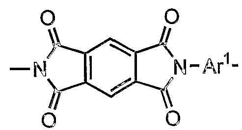
- a r 1 is a 1,4-phenylene group which may contain a non-reactive substituent.
- a wholly aromatic polyimide comprising a structural unit represented by the following formula, or 30 to 70 mol% of a structural unit represented by the above formula (1) and 70 to 70 mol% of a structural unit represented by the following formula (2)
- Ar 2a and Ar 2b are each independently an aromatic group having 6 to 20 carbon atoms which may contain a non-reactive substituent.
- the latter copolymerized wholly aromatic polyimide is particularly preferred.
- a r 1 in the above formula (1) may contain a non-reactive substituent 1, 4-phenylene group.
- Non-reactive substituents here include, for example, methyl group, ethyl Alkyl groups such as group, propyl group and cyclohexyl group, aromatic groups such as phenyl group and naphthyl group, halogen groups such as chloro group, fluoro group and bromo group, methoxy group, ethoxy group, phenoxy group And an alkoxyl group such as a group, a -toro group and the like.
- Ar 1 is, for example, a 2-chloro-1,4-phenylene group, a 2-bromo-1,4-phenylene group, a 2-methynolene 1,4-phenylene group, a 2-ethynolene 1,4 _Phenylene group, 2-cyclohexynole-1,4-phenylene group, 2-phenylene-1,4-phenylene group, 2-nitro-1,4-phenylene group, 2 —Methoxy-1,4-phenylene group, 2,5-dichloro-1,4-phenylene group, 2,6-dichloro-1′4-phenylene group, 2,5-diphenyl 1,4-phenylene group, 2,6-diphenyl 1,4-phenylene 2, 2, chloro-5-promo 1,4-phenylene 2, 2, chloro-5-fluoro 1 '4 1-phenylene group, 2,5-dimethylene 1,4-phenylene group, 2,6-dimethynolei 1,4-phenyl
- each A r 2 a and A r 2 b in the formula (2) independently is a non-reactive it contains a substituent good carbon number of 6 or more than 20 or less aromatic group.
- the non-reactive substituent herein may be the same as the 1 / non-reactive substituent described for Ar 1 in the above formula (1).
- Ar 2a and Ar 2b are 1,4-phenylene, 2-chloro-1,4-phenylene, 2-bromo-1,4-phenylene, 2-methylenol-1, 4-phenylene group, 2-ethynolene 1,4-phenylene group, 2-cyclohexylene 1,4-phenylene group-2.
- the glass transition point of the wholly aromatic polyimide in the present invention is 200 ° C. or higher. When the glass transition point is lower than 200 ° C., heat resistance of 1 ′′ is produced in a preferred embodiment of a semiconductor device manufacturing process.
- the upper limit is not particularly limited, and includes polyimide whose glass transition point is not observable even at 500 ° C. or higher.
- the glass transition point is the dynamic storage modulus E ′ obtained from the measurement. It was calculated from the value of the dynamic loss tangent ta ⁇ ⁇ calculated using the dynamic loss elastic modulus E ′′.
- the method for producing the wholly aromatic polyimide film is not particularly limited, and any conventionally known production method may be used.
- a raw material of the aromatic tetracarboxylic acid component part or all of the aromatic tetracarboxylic acid dianhydride or the aromatic tetracarboxylic acid component may be a dicarboxylic acid halide dicarboxylic acid alkyl ester derivative. . It is preferable to use aromatic tetracarboxylic dianhydride.
- the raw material of the aromatic diamine component may be an aromatic diamine or an amic acid-forming derivative of the aromatic diamine.
- some or all of the amino groups of the aromatic diamine component may be trialkylsilylated, or may be amidated with an aliphatic acid such as acetic acid. Among them, it is preferable to use an aromatic diamine substantially.
- These raw materials can be prepared, for example, in an organic polar solvent such as dimethyl-2-pyrrolidone dimethylacetamide and dimethylimidazolidinone.
- the polymerization reaction is carried out at a temperature of about C to 120 ° C. to obtain an organic polar solvent solution of the precursor polyamic acid or polyamic acid derivative, and the solution is cast on a support or the like, and then, for example, It is dried at about 800-400 ° C, and further subjected to a heat treatment at a maximum temperature of 250-600 ° C to cause imidization reaction to obtain a wholly aromatic polyimide film.
- a swelled gel film is obtained by chemically dehydrating a compound using a combination of an aliphatic acid anhydride such as xylcarposimide ⁇ or acetic anhydride and an organic nitrogen compound such as pyridin.
- a method in which the film is arbitrarily stretched and then subjected to constant-length drying and heat treatment to obtain a wholly aromatic polyimide film Japanese Patent Application Laid-Open No. 2002-179980.
- gel films obtained by chemical dehydration What is the method of manufacturing by stretching, depending on the stretching conditions? ft Flatness and number can be controlled, and it can be said that it is a particularly preferable manufacturing method in such applications.
- the wholly aromatic polyamide used in the heat bonding layer (C) of the present invention includes the following formula (3)
- Ar 3a and Ar 3b are each independently an aromatic group having 6 to 20 carbon atoms which may have a non-reactive substituent.
- an aromatic Jiamin component comprising A r 3 b of the aromatic dicarboxylic acid component and the formula (3) containing a A r 3 a in the formula (3) It is preferably an aromatic polyamide.
- An aromatic group of formula (3) in the A r 3 a and A r 3b are each independently a non-reactive substituent good carbon atoms 6 to have a 20.
- the non-reactive substituents that may be contained in Ar 3a and Ar 3b in the above formula (3) include, for example, alkyl such as methyl, ethyl, propyl, and cyclohexyl.
- aromatic groups such as a phenyl group and a naphthyl group; halogen groups such as a chloro group, a fluoro group and a promo group; .nitro group, a methoxy group, an ethoxy group and a phenoxy group.
- a r 3 a is an aromatic dicarboxylic acid component, terephthalic acid, Isofutaru acid, 1, 4-di Kano levo alkoxy naphthalene, 1, 5-Kano repo alkoxy naphthalene, 1, 8-dicaprate Roh levo carboxymethyl naphthalene 2, 6 Dicanoleboxinaphthalene, 2,7-dicarboxylic / repoxynaphthalene, 2,6-dicaboxianthracene, 2,7-dicaboxianthracene, 1,8-dicanoleboxianthracene, 2,4 dicanoleboxy Chitonolene, 2,5-dicanoreboxyl (m-xylene), 3,3, -dicarboxybiphenyl, 2,2, dicanolevoxybenzophenone, 4,4, dicanoreboxoxybenzo Phenonone, 3,3,1-dicanololepoxydiphenylenoate, 4,4, dicar
- aromatic dicarboxylic acid component Two or more aromatic dicarboxylic acid components can be used simultaneously.
- Preferred examples of the aromatic dicarboxylic acid component was, Q terephthalic acid, isophthalic acid unsaturated Example
- Ar 3b is an aromatic diamine component such as p-phenylenediamine, m-phenylenediamine, 1,4-diaminonaphthalene, 1,5-diaminonaphthalene, 1,8-diaminonaphthalene, 2, 6-diaminonaphthalene, 2,7-diaminonaphthalene, 2,6-diaminoanthracene, 2,7-diaminoanthracene, 1,8-diaminoanthracene, 2,4 diamino Toluene, 2,5-diamino (m-xylene), 2,5-diaminopyridine, 2,6-diaminopyridine, 3,5-diaminopyridine, 2,4 diaminotoluenebenzidine, 3,3,1-diaminobiphenyl, 2,2, diaminobenzophenone, 4,4,1-diaminobenzophenone, 3,3,1-diamin
- aromatic diamine components include p-phenylenediamine, m-phenylenediamine, 3,4 'diaminodiphenylenolate, 4,4, diaminodiphenylethenole and 1,3-bis-diamine.
- (3-aminophenoxy) benzene 5 is exemplified. More preferably, the aromatic diamine component is m-phenylenediamine.
- the above equation (3) becomes the following equation (3 _ 1) (3-1)
- the method for producing the heat-adhesive layer (C) comprising a wholly aromatic polyamide in the present invention is not particularly limited, and any conventionally known production method may be used.
- the polymer solution after polymerization may be used as it is, or the polymer is isolated and then redissolved in a solvent. May be.
- an organic polar solvent such as N-methyl-12-pyrrolidone, N, N-dimethylacetamide, N, N-dimethylformamide is preferable, but a strong acid such as concentrated sulfuric acid, concentrated nitric acid, and polyphosphoric acid.
- a solvent may be used.
- An inorganic salt such as calcium chloride, magnesium chloride, lithium chloride or lithium nitrate can be added to the aromatic polyamide solution as a dissolution aid, if desired.
- the polymer concentration in the solution is preferably about 1 to 60% by weight, and more preferably 3 to 40% by weight! / ,.
- the polymer solution prepared as described above is cast (also called casting) on a substrate (A) composed of a wholly aromatic polyimide film or an adherend (B) composed of an inorganic material, and the solvent is dispersed by drying. Let it.
- Examples of the casting method include a die extrusion method, a method using an applicator, and a method using a coater.
- the temperature of the polymer solution at the time of casting is not particularly limited, and the polymer solution is selected so that the viscosity of the polymer solution is in the range of 30 to 200,000 Poise. Is preferred. More preferably, 50 to 20,000 Poise is exemplified.
- Drying methods for scattering the solvent include drying by hot mouth heat, vacuum heating, infrared Hfti heat, and microwave mouth wave heating. Heat drying by hot air is preferred! / ,.
- the drying temperature at this time is 30. C to 400 ° C, more preferably 40 ° C to 350 ° C, and still more preferably 70 ° C to 300 ° C.
- the thickness of the heat-adhesive layer (C) made of a wholly aromatic polyamide in the present invention is preferably in the range of 0.1 to 10000 im. If the value is less than 0. ⁇ , the precision of adhesion to the adherend ( ⁇ ) made of inorganic material cannot be obtained, and the flatness and smoothness of the contact surface of the crimping machine are required, and the flatness and smoothness are required. Poor control of the properties, More often. If it is larger than 2000 im, it is difficult for heat to be transmitted when bonding to the adherend (B) made of an inorganic material, and it takes time S to transmit the temperature, which may lower productivity.
- the surface roughness of the heat-adhesive layer (C) made of a wholly aromatic polyamide in the present invention is not particularly limited, but the surface roughness (Rt) is in the range of 0.01 ⁇ to 100 ⁇ m. Is preferred. When the thickness is less than 0.01 ⁇ m, the solvent may not penetrate when the resin is impregnated and peeled, and peeling may be difficult. When the thickness is more than 100 ⁇ m, the adhesion to the adherend (B) made of an inorganic material may occur. Insufficient adhesion accuracy often results in uneven adhesion.
- the laminate of the present invention provides a base (A) made of a wholly aromatic polyimide film having a glass transition point of 200 ° C or more.
- an inorganic material (B) When the base material (A) and the adherend made of a silicon wafer are laminated, the base material (A) becomes
- peel strength is less than 0.1 IN / m, sufficient adhesive strength to pass through the semiconductor device manufacturing process may not be obtained, and the semiconductor chip may fall off the substrate during the process.
- the peel strength here refers to a 1 cm wide sheet-shaped bonded body that has been thermocompressed at 370 ° C and 5.0 to 6.OMPa for 15 minutes at 25 ° C.
- N average peeling force
- the substrate (A) is represented by the following formula (1)
- a r 1 is a 1,4-phenylene group which may contain a non-reactive energizing group.
- the base material (A) is composed of 30 to 70 mol% of the structural unit represented by the above formula (1) and the following formula (2) ... (2)
- At 23 Oyobi are each independently a non-reactive it may also contain a substituent group V, an aromatic group having 6 to 20 carbon atoms. ]
- the base material (A) has an imide group concentration (equivalent / kg) calculated based on the following formula (4).
- the substrate (A) made of a wholly aromatic polyimide film and the inorganic material (B) were heated at 180 ° C to 600 ° C.
- the laminate (1 ′) can be obtained by thermocompression bonding at a temperature of C and a pressure of 0.001 MPa to 1000 MPa for 0.1 second to 48 hours. Adhesion conditions such as temperature, pressure, and time can be arbitrarily controlled by the material or combination of the adhesive sheet and the adherend to be used.
- the temperature for thermocompression bonding is in the range of 1.80 ° C. to 600 ° C., preferably in the range of 180 ° C. to 550 ° C., and more preferably in the range of 180 ° C. to 500 ° C.
- the pressure of thermocompression bonding is The average pressure applied to the whole and the adherends is in the range of 0.001 MPa to 1000 MPa ', and preferably in the range of 0.0 IMP a to 10 OMPa. If the pressure is less than 0.001 MPa, it is not possible to bond sufficiently. If the pressure is higher than 10 OMPa, the adherend may be damaged.
- the pressure holding time of the thermocompression bonding is in the range of 0.1 second to 48 hours. If the holding time is less than 0.1 second, the adhesive strength becomes insufficient, and it becomes difficult to obtain a laminated body having a stable adhesive strength. If the time is longer than 48 hours, productivity will decrease. More preferably, the pressure holding time of the thermocompression bonding is more preferably in the range of 1 second to 24 hours.
- thermocompression bonding after increasing the temperature and bonding at a predetermined pressure for a predetermined time, it may be allowed to cool while being pressed at room temperature for a predetermined time. After bonding for a period of time, the temperature may be kept constant for a certain period of time with the pressure released.
- the base material (A) whose adhesive sheet is composed of a wholly aromatic polyimide film and the thermal bonding layer (C) composed of a wholly aromatic polyamide whose glass transition point is 200 ° C to 500 ° C
- the laminate of the present invention comprises a substrate (A) made of a wholly aromatic polyimide film, which is obtained by further laminating an inorganic material (B) on the thermal adhesive layer (C) of the adhesive sheet. (C) and an inorganic material (B) in this order.
- the base material (A) made of a wholly aromatic polyimide film is converted into an inorganic material (B) via a heat bonding layer (C) made of a wholly aromatic polyamide having a glass transition point of 200 to 500 ° C.
- the laminate (I) can be obtained by thermocompression bonding at a temperature of 180 ° C. to 600 ° C. and 0.00 IMP a to a pressure of 1000 MPa for 0.1 second to 1 hour. it can.
- Adhesion conditions such as temperature, pressure and time can be controlled arbitrarily according to the material or combination of the adhesive sheet and the adherend.
- the thermocompression bonding temperature is in the range of 180 ° C to 600 ° C, preferably in the range of 180 ° C to 550 ° C, and more preferably. More specifically, it is in the range of 180 ° C to 500 ° C.
- the pressure of the thermocompression bonding is 0.01 MPa to 100 MPa as an average pressure applied to the entirety of the adhesive sheet and the object to be bonded, and preferably 0.0 MPa. Ll 0 OMPa. If the pressure is less than 0.000 MPa, it is not possible to bond sufficiently, and if the pressure is higher than 100 MPa, the adherend may be thin.
- the pressure holding time of thermocompression bonding can be set in a short time by providing the heat bonding layer, and is in a range of 0.1 second to 1 hour.
- the time is less than 0.1 second, the adhesive strength becomes insufficient, and it becomes difficult to obtain a laminate having a stable adhesive strength.
- the holding time of the thermocompression bonding is more preferably in the range of 1 second to 30 minutes.
- thermocompression bonding after increasing the temperature and bonding at a predetermined pressure for a predetermined time, it may be allowed to cool while being pressed at room temperature for a predetermined time. After bonding for a period of time, the temperature may be kept constant for a certain period of time with the pressure released.
- the inorganic material (B) in the present invention means a material whose 60% by volume or more is composed of an inorganic compound.
- the inorganic compound include metals such as aluminum, iron, silicon, germanium, and carbon; nitride compounds such as barium titanate, potassium titanate, titanium nitride, titanium nitride, and boron nitride; zirconium oxide; and aluminum oxide.
- ceramic such as Serazine ⁇ manufactured by Mitsubishi Gas Chemical Company, and glass.
- semiconductor metals such as silicon and germanium, and more preferred are silicon wafers.
- Examples of the form of these inorganic materials and the adherend made of the inorganic materials include cloth, mesh, inorganic sintered body, porous, plate-like, sheet-like, and film-like, and are preferably porous, plate-like. , Sheet-like. Therefore, for example, a plate made of a carbon-epoxy composite manufactured from a so-called prepredder, and a composite made of an inorganic material such as a porous ceramics-based epoxy compound are included in the adherend made of an inorganic material.
- the thickness of the inorganic material of the adherend is not particularly limited, ⁇ ! ⁇ 2 In many cases, it is preferable to be in the range of 0.000 ⁇ m. If the thickness is less than 1 ⁇ m, the accuracy of the crimping device is required when bonding with the bonding sheet, and it may be difficult to bond the bonding surface uniformly without unevenness. In addition, there is a case where the sheet may be broken during crimping without obtaining sufficient mechanical strength for crimping. When the thickness is more than 2000 m, heat is not easily transmitted when bonding to an adhesive sheet, and it takes time to transmit the temperature, which may lower productivity.
- an object layer (D), an organic protective layer (E), a ⁇ base material ( ⁇ ) made of a wholly aromatic polyimide film, a heat bonding layer (C), and an inorganic material (B) are arranged in this order.
- the present invention provides a substrate layer (A) made of a wholly aromatic polyimide film having a glass transition point of 200 ° C. or more, and an inorganic material (D), an organic material protective layer (E), and an inorganic material (D). B) are laminated in this order.
- the material layer (D) to be processed is not particularly limited as long as it can be bonded to the following organic material protective layer (E) by any force, but a semiconductor substrate that has been subjected to a circuit component forming step including impurity introduction is used. It is mentioned as a preferable application of the present invention. At this time, it is preferable that the grace fee (B) is a holding substrate.
- the organic material protective layer (E) is used for the purpose of protecting the object layer (D).
- the processing object layer (D) is a semiconductor substrate on which a circuit component forming step including impurity introduction has been performed
- polyimide fluorinated polyimide, polyorganohydridosilane, polysiloxane, polysiloxane-modified polyimide, Polyphenylene, polybenzyl, polyaryl ether and the like are used, and more preferably, polysiloxane modified polyimide is used.
- the method for laminating the laminate is not particularly limited, but the above-mentioned adhesive sheet and the adherend are bonded together at room temperature, and in some cases, by heating and applying pressure.
- Bonding methods include bonding by a press using a heating press or a vacuum press, and bonding by a roller.
- a metal such as stainless steel, iron, titanium, aluminum, copper, or the like or an alloy thereof between the top plate of the heating press machine and the above-mentioned adhesive sheet and the adherend.
- Adhesion conditions such as temperature, pressure, and time are not particularly limited, but can be arbitrarily controlled at the time of adhesion by a material to be used and a material or a combination of adherends.
- a suitable temperature at the time of bonding for example, a range of 180 ° C. to 600 ° C. can be exemplified. Preferably it is in the range of 180 ° C to 550 ° C.
- the pressure at the time of bonding is, as an average pressure applied to the entirety of the adhesive sheet and the adherend, in the range of 0.000 MPa to 100 MPa, and preferably 0.0 IMPa. MPa to l0OMPa. If the pressure is less than 0.001 MPa, it is not possible to bond sufficiently. If the pressure is higher than 100 MPa, the adherend may be damaged.
- the pressure holding time during bonding is preferably in the range of 0.1 second to 48 hours. When the time is less than 0.1 second, the adhesive strength becomes insufficient, and it becomes difficult to obtain a laminate having a stable adhesive strength.
- the pressure holding time for bonding is more preferably in the range of 1 second to 24 hours.
- heat bonding can be performed in a short time.
- the mixture When bonding, after increasing the temperature and bonding at a predetermined pressure for a predetermined time, the mixture may be left to cool while being pressed at room temperature for a predetermined time, or may be raised at a predetermined pressure at a predetermined pressure for a predetermined time. After bonding, the temperature may be kept constant for a certain period of time with the pressure released.
- the present invention provides an object layer (D), an organic protective layer (E), a substrate (A) made of a wholly aromatic polyimide film having a glass transition point of 200 ° C. or more, and inorganic
- the exposed surface of the D layer is subjected to a thin-layer treatment to form a D 'layer, comprising a D' layer, an E layer, an A layer, and a B layer.
- the interface between the E layer and the A layer is peeled off to obtain a laminate (IV) comprising the D 'layer and the E layer, thereby producing a laminate (IV). Is the way.
- thermal adhesive layer (C) made of wholly aromatic polyamide having a glass transition point of 200 to 500 ° C between the substrate (A) and the inorganic material (B).
- the thermal adhesive layer (C) composed of a wholly aromatic polyamide has the following formula (3-1).
- the polymer comprises a structural unit represented by
- Substrate (A) has the following formula (1)
- a r 1 is a 1,4-phenylene group which may contain a non-reactive substituent.
- It is composed of a wholly aromatic polyimide composed of a structural unit represented by the following formula. It is preferably composed of a polymer.
- the base material (A) is composed of 30 to 70 mol% of the structural unit represented by the above formula (1) and the following formula (2) ... (2)
- a r 2a and A r 2 b each independently is a non-reactive contain a substituent good carbon number of 6 or more than 20 or less aromatic group.
- a polymer made of a wholly aromatic polyimide consisting of 70 to 30 mol% of a structural unit represented by the following formula.
- the method of laminating the laminate (III) is not particularly limited, It can be obtained in the same manner as described for the fields ( ⁇ ) and (ir).
- the processing target layer (D) is a semiconductor substrate that has been subjected to a HI path component formation process including impurity introduction, and the inorganic material (B) is a holding substrate.
- the exposed surface of the D layer is polished and thinned.
- the interface between the organic protective layer (E) and the base material (A) is peeled off, and the semiconductor' substrate (D 'layer)' and the organic protective layer are separated.
- One of the preferred applications of the method for producing a laminate according to the present invention is to obtain a laminate for a semiconductor component comprising (E).
- a thermal bonding layer (C) made of all aromatic polyamide having a glass transition point of 200 ° C to 500 ° C can be provided between the base material (A) and the inorganic material (B). preferable.
- the interface between the E layer and the A layer is peeled off, and the interface between the E layer and the A layer is obtained when a laminate (IV) composed of the D 'layer and the E layer is obtained.
- Preferred examples of the peeling method include the following four methods.
- a laminate composed of the layer D, the layer E, the layer A, (preferably the layer C), and the layer B is immersed in a liquid.
- the liquid After infiltrating into the interface between the E layer and the A layer, the liquid is rapidly heated to a temperature higher than the boiling point of the liquid to vaporize the liquid that has permeated the interface (method 1).
- the immersion condition of the liquid is preferably 30 ° C. or higher. More preferably, it is 40 ° C. or higher and the boiling point of the liquid or lower. At a temperature lower than 30 ° C, the liquid does not easily penetrate between the layers, making it difficult to peel off.
- the immersion time is preferably 1 minute or more. More preferably, it is 30 minutes or more.
- a method may be used in which the laminate is exposed to the vapor of the liquid and then cooled to dew the liquid between the layers.
- the heating conditions after immersion are preferably higher than the boiling point of the liquid. More preferably, it is 50 ° C. or higher than the boiling point of the liquid.
- the heating time is preferably raised to a desired temperature within 5 minutes. More preferably, it is within 30 seconds. If the time is longer than 5 minutes, the effect of volume expansion due to gas is difficult to obtain, and peeling becomes difficult.
- the liquid may be a liquid having a boiling point of 30 ° C. or more at normal pressure, and preferably a liquid having a boiling point of 40 ° C. or more and 200 ° C. or less.
- liquids include water, methanol, ethanol, 1-propanol, 2-propanol, 1-butanol, 2-butanol, tert-butanol, 1-pentanol, 2-pentanol, and acetone.
- water, methanol, ethanol, and isopropanol are suitably used. More preferably, water is suitably used.
- a laminate composed of the layer D ', the layer E, the layer A (preferably the layer C), and the layer B is immersed in water to remove the layer.
- After infiltrating water at the interface between the layer and layer A there is a method of cooling to 0 ° C or less, coagulating the water that has permeated the interface, and peeling it off (method 2).
- the water immersion condition is preferably 30 ° C. or higher. More preferably, it is 40 ° C. or more and 100 ° C. or less. At a temperature lower than 30 ° C, water hardly permeates between the layers, and peeling becomes difficult.
- the time is preferably 1 minute or more. More preferably, it is 5 minutes or more. If the time is shorter than 1 minute, the penetration is not promoted and the peeling becomes difficult, which is not preferable.
- a method may be employed in which the laminate is exposed to water vapor and then cooled to condense water between the layers.
- the cooling condition after immersion is preferably 0 ° C. or less. More preferably, it is ⁇ 5 ° C. or lower.
- As the cooling time it is preferable to cool to a desired temperature within 10 minutes. More preferably, it is within 30 seconds. If the time is longer than 10 minutes, it is difficult to obtain the effect of volume expansion due to solidification, and peeling is difficult.
- a third method for peeling the interface between the E layer and the A layer 30% is applied in the thickness direction of the laminate including the D ′ layer, the E layer, the A layer (preferably, the C layer) and the B layer.
- a method of separating the interface between the E layer and the A layer by generating a temperature difference of 800 ° C. (method 3).
- the method for generating the temperature difference is not particularly limited. Force The method of moving the laminate from a low-temperature state to a high-temperature state, the method of moving from a high-temperature state to a low-temperature state, or a method of generating the temperature difference between the inorganic material layer B side and the material layer D to be treated.
- Can be The method of moving the laminate from a low-temperature state to a high-temperature state or a method of moving from a high-temperature state to a low-temperature state includes, for example, room temperature conditions in air or liquid, hot air heating, steam heating, vacuum heating, infrared heating, and the like.
- heating conditions such as heating by contact using a hot plate, hot mouth, water bath, oil bath, TEG path, salt bath, solder bath, etc., and cool air, dry ice, ice, and cooling liquid Any state may be used as long as a temperature difference occurs in each state of the cooling state of the body.
- a method of generating the temperature difference in the thickness direction of the laminated body a method of generating the above-mentioned state on each surface may be used, and a method of shifting may be used I ′.
- a method of shifting there is a method in which dry ice, ice, and a cooling liquid are brought into contact from above the laminated body placed on a hot plate.
- the temperature difference is from 30 to 800 ° C., preferably from 100 to 600 ° C.
- a laminate comprising the D 'layer, the E layer, the A layer (preferably, the C layer), and the B layer has a pH value.
- a method of immersing in an alkaline solution having a pH of 8 to 14 and infiltrating the A layer with the alkaline solution to peel off the interface between the E layer and the A layer (method 4).
- the alkaline solution is more preferably an aqueous solution containing ammonia at a pH value of 10 to 14, more preferably 0.1% to 30%.
- the solvent used for the alkaline solution is not particularly limited as long as it dissolves the alcohol, but is preferably water.
- the temperature is preferably 15 ° C to 120 ° C. If the temperature is lower than 15 ° C, the water in the aqueous solution freezes. I don't like it because the water boiled down.
- the immersion time is preferably from 1 second to 360.000 seconds, and if it is less than 1 second, it does not sufficiently penetrate into the film part, making it difficult to peel off.If it is more than 360 seconds, the process time is long. And productivity becomes worse.
- the measurement was performed by Orientec UCT-1T at a pulling speed of 5 mm / min.
- the Young's modulus was determined from the stress (GPa) when the elongation was set to 100% from the initial gradient of the elongation-stress curve of the data obtained by the measurement.
- the bonded body and the adhesive of Example 3 are 300 ° C, and the adhesives of Examples 1, 2, 4 and 17 are 370 ° C.
- the measurement was performed using Orientec UCT-1T.
- the average peel force (N) was calculated from the curve of the gripper travel distance over at least 10 Omm of the peel length excluding the first 25 mm, and was calculated as the value per lm width (NZm).
- the temperature was raised in the range of 50 ° C. to 500 ° C., and the measurement was performed at a frequency of 6.28 rad / s with Rh eometrics R SAI I.
- the glass transition point was calculated from the value of the dynamic loss tangent t a ⁇ ⁇ calculated from the dynamic storage ⁇ I “live rate E ', dynamic loss elastic modulus E” obtained from the measurement.
- the central part of the used silicon wafer 1.2 mm x 0.92 mm, was measured with a non-contact three-dimensional micro surface shape observation system NT-2000 (WYKO). Adhesive sheet production example 1.
- the resulting polyamic acid solution was cast on a glass plate using a doctor blade with a thickness of 1.0 mm, and a 30 ° C dehydration / condensation bath consisting of 250 ml of acetic anhydride, 74 g of triethylenediamine and 2000 ml of NMP. Immersed in water for 30 minutes The resultant was separated from a glass plate as a support to obtain a gel film.
- the obtained gel film was immersed in NMP at room temperature for 20 minutes for washing.Then, both ends of the gel film were chuck-fixed, and at room temperature, 1 Omrn / 1.05 times in two orthogonal directions at room temperature. Simultaneous biaxial stretching was performed at a speed of sec. The swelling degree of the gel film at the start of stretching was 1510%. (The degree of swelling was calculated from the ratio of the weight of dry condition with a swollen state.
- the adhesive sheet has the following formula (1-1a) (1-a)
- Table 1 shows the film thickness, strength, Young's modulus, glass transition temperature, and linear thermal expansion coefficient of P-1.
- polyamic acid As a viscous solution, polyamic acid was used. An NMP solution was obtained. The concentration of the obtained polyamic acid NMP was 13 wt%. The obtained 13 wt% polyamic acid NMP solution was cast on a glass plate using a doctor blade having a thickness of 1.0 mm, and acetic anhydride 100, 500 ml, pyridine 450, and NMP 150 It was immersed in a 30 ° C. dehydration / condensation bath composed of O′m1 for 30 minutes to be imidized, and separated from the glass plate as a support to obtain a gel film.
- the stretched gel film was fixed in a frame, and heated with a hot air drier using dry air.
- the temperature was raised in stages from C to 300 ° C, and drying and heat treatment were performed.
- the temperature was raised in a multi-stage manner from 300 ° C. to 450 ° C. using a hot air circulation type open to obtain a whole aromatic polyimide.
- the adhesive sheet has the following formula (1-1a)
- the adhesive sheet is a wholly aromatic polymer consisting of 50 mol% of structural units represented by Hereinafter, the adhesive sheet thus obtained is abbreviated as P-2.
- Table 1 shows the film thickness, strength, Young's modulus, glass transition temperature, and coefficient of linear thermal expansion of P-2. Table 1
- Silicon wafer (6 inch diameter, thickness 60 ⁇ ⁇ m, surface roughness (R t) about 0.02 / im, linear thermal expansion ⁇ number + 4.15 ppm / .C) as an adherend made of inorganic material
- a wholly aromatic polyimide film P-1 was sandwiched between gold plates and set in a heating press. After adjusting the surface temperature of the actual contact surface to 370 ° C with a heating press machine, it was pressed and bonded at 5.5 MPa for 15 minutes. The press was turned off, allowed to cool to 250 ° C, and removed from the press.
- the peel strength at the interface between the obtained wholly aromatic polyimide film P-1 and silicon ueno was 15. ONZm.
- the absolute value of the difference in linear thermal expansion coefficient between the wholly aromatic polyimide film P-1 and the silicon wafer is 12.75 ppm / ° C. ⁇ Example 2
- a laminate was obtained in the same manner as in Example 1, except that the adhesive sheet was a wholly aromatic polyimide film (P-2). As a result, the peel strength at the interface between the obtained wholly aromatic polyimide film P-12 and the silicon wafer was 32.5 NZm. The absolute value of the linear thermal expansion difference between the wholly aromatic polyimide film P-2 and the silicon wafer is 1.60 p ⁇ mZ ° C.
- the adhesive sheet was a wholly aromatic polyimide film (P-2).
- the powder of Conex ⁇ manufactured by Teijin Techno Products Co., Ltd. was dispersed in N-methyl-2-pyrrolidone at 5 ° C and then dissolved at 40 ° C to obtain a 10 wt% solution.
- the 10 wt% Conex® solution was cast on a wholly aromatic polyimide film P-1 stuck on a glass plate using a 28 jum thickness bar coater. After that, it is dried at 160 ° C for 30 minutes with a hot air dryer, then heated up to 280 ° C in multiple stages, and dried and heat-treated to form a thermal bond made of a wholly aromatic polyamide film.
- An adhesive sheet having a layer (C) was obtained.
- the thermal adhesive layer (C) of the adhesive sheet is placed on a silicon wafer (6 inches in diameter, 600 m in thickness, surface roughness (Rt) of about 0.02 im) as an adherend made of inorganic material. After placing it in close contact, it was sandwiched between gold plates and set in a heating press. The surface temperature of the actual contact surface was set to 300 ° C with a heating press machine, and then pressed at 5.5 MPa for 2 minutes for bonding. Thereafter, it was taken out of the press machine and allowed to cool. The peel strength at the interface between the thermal bonding layer (C) and the silicon wafer in the obtained laminate was 20 ⁇ shear peel strength was 170 N / cm 2 . '' Example 4
- a wholly aromatic polyimide film P-1 was changed to a wholly aromatic polyimide film (Kapton (registered trademark) 5 OH manufactured by Toray DuPont), and the heat bonding temperature was set to 370 ° C.
- An adhesive sheet having a thermal adhesive layer (C) made of a wholly aromatic polyamide film was obtained.
- the thermal adhesive layer (C) of the adhesive sheet on a silicon wafer (6 inch diameter, thickness 600 ⁇ , surface 3 ⁇ 4 ⁇ (R t) about 0.02 ⁇ m) as an adherend made of inorganic material After that, it was sandwiched between gold plates and set in a force B heat press. After adjusting the surface temperature of the actual contact surface to 300 ° C with a heating press machine, it was pressed and adhered at 5.5 MPa for 2 minutes. Thereafter, it was taken out of the press machine and allowed to cool. The peel strength at the interface between the thermal bonding layer (C) and the silicon wafer in the obtained laminate was 20 ONZm.
- a polyimide coating layer as an organic protective layer (E), and silicon having a thickness of 0.6 mm and a diameter of 15 Omm were formed.
- the stacked wafers were set in a hot press and pressed at 5 MPa, 300 ° C for 2 minutes. That is, a silicon wafer (holding substrate), a Conex® layer, a wholly aromatic polyimide film P-1, an organic protective layer (E), and a silicon wafer (semiconductor substrate) were sequentially stacked.
- the exposed side of the silicon wafer (semiconductor substrate) of this laminated body was set in a polishing machine, and polished using a polishing paper containing silicon carbide particles under a load of 160 gf Zcm 2.
- the polishing plate was rotated at 110 rpm, and polished until the silicon wafer thickness became 130 m. Polishing was performed in the order of # 150, # 800, and # 200. No peeling of the laminate was observed during polishing.
- the obtained laminate was immersed in water at 60 ° C. for 1 hour and taken out. Next, it was set on a hot plate at 200 ° C. for 30 seconds, taken out, and then returned to room temperature.
- the ground body produced in the same manner as in Example 5 was immersed in water at 100 ° C. for 1 minute. Next, it was set on a hot plate at 200 ° C for 30 seconds, taken out, and then returned to room temperature.
- the ground laminate produced in the same manner as in Example 5 was exposed to steam of 3 kgf / cm 2 for 1 minute. Then, it was immediately immersed in water at 20 ° C for 3 seconds and taken out. Next, it was set on a hot plate at 200 ° C. for 30 seconds, taken out, and returned to room temperature.
- the ground laminate formed in the same manner as in Example 5 was immersed in methanol at 30 ° C. for 1 hour. Next, it was set on a hot plate at 200 ° C. for 30 seconds, taken out, and then returned to room temperature.
- the ground laminate formed in the same manner as in Example 5 was immersed in ethanol at 50 ° C. for 1 hour. Next, it was placed on a hot plate at 200 ° C. for 30 seconds, taken out, and then returned to room temperature.
- the laminate was easily peeled off at the interface between the polyimide coat layer and the aromatic polyimide film P-1.
- the interfaces between the silicon wafer (holding substrate), the Conex ⁇ layer, and the aromatic polyimide film P-1 did not peel off.
- Example 11 The ground laminate produced in the same manner as in Example 5 was immersed in isopropanol at 80 ° C. for 1 hour. Next, it was placed on a hot plate at 200 ° C. for 30 seconds, taken out, and then returned to room temperature. The laminate easily peeled off at the interface between the polyimide coat layer and the aromatic polyimide film P-1. The interface between the silicon wafer (holding substrate), the Conex ⁇ layer, and the aromatic polyimide film P-1 did not peel off.
- Example 11 The ground laminate produced in the same manner as in Example 5 was immersed in isopropanol at 80 ° C. for 1 hour. Next, it was placed on a hot plate at 200 ° C. for 30 seconds, taken out, and then returned to room temperature. The laminate easily peeled off at the interface between the polyimide coat layer and the aromatic polyimide film P-1. The interface between the silicon wafer (holding substrate), the Conex ⁇ layer, and the aromatic polyimide film P-1 did not peel off.
- the ground laminate produced in the same manner as in Example 5 was immersed in water at 60 ° C. for 1 hour and taken out. Next, it was placed in liquid nitrogen for 30 seconds, taken out, and then returned to room temperature.
- the ground body produced in the same manner as in Example 5 was immersed in water at 100 ° C. for 1 minute. Next, it was placed in liquid nitrogen for 30 seconds, taken out, and then returned to room temperature.
- the laminate is easy at the interface between the polyimide coat layer and the aromatic polyimide film P-1 Was peeled off.
- the interfaces between the silicon wafer (holding substrate), the Conex® layer, and the aromatic polyimide film P-1 did not peel off.
- the ground laminate produced in the same manner as in Example 5 was exposed to steam of 3 kgf / cm 2 for 1 minute. Then, it was immediately immersed in water at 20 ° C for 3 seconds and taken out. Next, it was placed in liquid nitrogen for 30 seconds, taken out, and then returned to room temperature.
- Example 15 After the ground body produced in the same manner as in Example 5 was placed on a hot plate at 300 ° C. with the holding substrate face down, ice was placed on the silicon wafer (semiconductor substrate) face to cool it. The laminate easily peeled off at the interface between the polyimide coat layer and the aromatic polyimide film P-1. The interfaces between the silicon wafer (holding substrate), the Conex ⁇ layer, and the aromatic polyimide film P-1 did not peel off.
- Example 15 Example 15
- Example 16 The laminated body prepared in the same manner as in Example 5 was placed on a hot plate at 400 ° C. with the holding substrate face down, and then cooled by flowing liquid nitrogen over the silicon wafer (semiconductor substrate) surface. The laminate easily peeled off at the interface between the polyimide coat layer and the aromatic polyimide film P-1. The interfaces between the silicon wafer (holding substrate), the Conex ⁇ layer, and the aromatic polyimide film P-1 did not peel off.
- Example 16 Example 16
- Example 1 7 The ground laminate produced in the same manner as in Example 5 was immersed in a 25% aqueous ammonia solution at room temperature. After 3 hours, it was confirmed that the laminate was peeled off, and was taken out. The laminate was peeled off at the interface between the polyimide coat layer and the aromatic polyimide-1 and the aromatic polyimide film was completely dissolved. Also, the interface between the holding substrate and the aromatic polyamide layer was peeled off.
- a silicon wafer (holding substrate), a wholly aromatic polyimide film P-2, a polyimide coating layer, and a silicon-evaporated silicon wafer (semiconductor substrate) with a thickness of 0.6 mm and a diameter of 15 Omm are laminated in this order, and hot-pressed. It was set and pressed at 5.5 MPa, 370 ° C. for 15 minutes. That is, a silicon wafer (holding substrate), a wholly aromatic polyimide film P-2, a polyimide coat layer, and a silicon wafer (semiconductor substrate) were sequentially stacked.
- the exposed side of the silicon wafer (semiconductor substrate) of this laminate was set on a polishing machine, and the polishing plate was rotated at 110 rpm using a polishing paper containing silicon carbide particles under a load of 160 gf Zcm 2. And polished until the silicon wafer thickness was 130 ⁇ m. Polishing was performed at # 150, # 800, and # 2000 grain sizes. No peeling of the laminate was observed during polishing.
- the ground laminate was immersed in a 25% aqueous ammonia solution at room temperature. After 3 hours, it was confirmed that the laminated body had peeled off, and was taken out.
- the laminate had the aromatic polyimide film P-2 completely dissolved, and peeled off at the interface between the polyimide coat layer and the aromatic polyimide film P_2! / ⁇ .
Landscapes
- Chemical & Material Sciences (AREA)
- Organic Chemistry (AREA)
- Adhesives Or Adhesive Processes (AREA)
- Laminated Bodies (AREA)
- Adhesive Tapes (AREA)
- Processing And Handling Of Plastics And Other Materials For Molding In General (AREA)
Abstract
Description


Claims


Priority Applications (5)
| Application Number | Priority Date | Filing Date | Title |
|---|---|---|---|
| US10/543,813 US20060134407A1 (en) | 2003-01-31 | 2004-01-28 | Adhesive sheet and layered product |
| EP04705907A EP1589086A4 (en) | 2003-01-31 | 2004-01-28 | ADHESIVE AND LAYER BODY |
| CA 2513122 CA2513122A1 (en) | 2003-01-31 | 2004-01-28 | Adhesive sheet and laminate |
| JP2005504729A JP4266980B2 (ja) | 2003-01-31 | 2004-01-28 | 接着シートおよび積層体 |
| KR1020057010070A KR101086662B1 (ko) | 2003-01-31 | 2004-01-28 | 접착시트 및 적층체 |
Applications Claiming Priority (4)
| Application Number | Priority Date | Filing Date | Title |
|---|---|---|---|
| JP2003-023367 | 2003-01-31 | ||
| JP2003023367 | 2003-01-31 | ||
| JP2003-271782 | 2003-07-08 | ||
| JP2003271782 | 2003-07-08 |
Publications (1)
| Publication Number | Publication Date |
|---|---|
| WO2004067666A1 true WO2004067666A1 (ja) | 2004-08-12 |
Family
ID=32828922
Family Applications (1)
| Application Number | Title | Priority Date | Filing Date |
|---|---|---|---|
| PCT/JP2004/000757 Ceased WO2004067666A1 (ja) | 2003-01-31 | 2004-01-28 | 接着シートおよび積層体 |
Country Status (7)
| Country | Link |
|---|---|
| US (1) | US20060134407A1 (ja) |
| EP (1) | EP1589086A4 (ja) |
| JP (1) | JP4266980B2 (ja) |
| KR (1) | KR101086662B1 (ja) |
| CA (1) | CA2513122A1 (ja) |
| TW (1) | TW200502348A (ja) |
| WO (1) | WO2004067666A1 (ja) |
Cited By (6)
| Publication number | Priority date | Publication date | Assignee | Title |
|---|---|---|---|---|
| JP2006255926A (ja) * | 2005-03-15 | 2006-09-28 | Teijin Ltd | 積層フィルム |
| JP2007201069A (ja) * | 2006-01-25 | 2007-08-09 | Teijin Ltd | 太陽電池形成用ポリイミドフィルム |
| JP2008118069A (ja) * | 2006-11-08 | 2008-05-22 | Toyobo Co Ltd | 半導体装置 |
| EP1698460A4 (en) * | 2003-12-24 | 2009-05-06 | Teijin Ltd | MULTILAYER BODY |
| WO2019066225A1 (ko) * | 2017-09-27 | 2019-04-04 | 주식회사 제이에이치씨 | 내열성 및 내습성이 우수한 전도성 접착 필름 |
| JP2021191630A (ja) * | 2020-06-03 | 2021-12-16 | 積水化学工業株式会社 | 半導体加工用積層体、及び、被処理部材の処理方法 |
Families Citing this family (4)
| Publication number | Priority date | Publication date | Assignee | Title |
|---|---|---|---|---|
| KR100910672B1 (ko) * | 2007-08-03 | 2009-08-04 | 도레이새한 주식회사 | 내열성 점착시트 |
| WO2014147033A1 (de) * | 2013-03-18 | 2014-09-25 | Behr Gmbh & Co. Kg | Schichtwärmeübertragungseinrichtung und verfahren zur herstellung einer schichtwärmeübertragungseinrichtung |
| JP6633534B2 (ja) * | 2014-10-06 | 2020-01-22 | 日東電工株式会社 | 薬液処理用マスキングシート |
| JP7450356B2 (ja) * | 2018-09-28 | 2024-03-15 | 帝人株式会社 | 熱変性ポリマー層-無機基材複合体、ポリマー部材-無機基材複合体、及びそれらの製造方法 |
Citations (3)
| Publication number | Priority date | Publication date | Assignee | Title |
|---|---|---|---|---|
| JPH05263049A (ja) * | 1992-03-19 | 1993-10-12 | Kanegafuchi Chem Ind Co Ltd | Tab用テープ及び該製造方法 |
| JP2002256237A (ja) * | 2001-03-01 | 2002-09-11 | Hitachi Chem Co Ltd | 接着シート、半導体装置の製造方法および半導体装置 |
| JP2002256238A (ja) * | 2001-03-05 | 2002-09-11 | Hitachi Chem Co Ltd | 接着フィルム、それを用いた半導体装置の製造方法及び半導体装置 |
Family Cites Families (6)
| Publication number | Priority date | Publication date | Assignee | Title |
|---|---|---|---|---|
| JPH0878785A (ja) * | 1994-08-31 | 1996-03-22 | Sharp Corp | 半導体レーザ素子およびその製造方法 |
| JP2961642B2 (ja) * | 1995-05-31 | 1999-10-12 | 株式会社巴川製紙所 | 電子部品用接着テープおよび液状接着剤 |
| TW326566B (en) * | 1996-04-19 | 1998-02-11 | Hitachi Chemical Co Ltd | Composite film and lead frame with composite film attached |
| JPH10275752A (ja) * | 1997-03-28 | 1998-10-13 | Ube Ind Ltd | 張合わせウエハ−及びその製造方法、基板 |
| US6379784B1 (en) * | 1999-09-28 | 2002-04-30 | Ube Industries, Ltd. | Aromatic polyimide laminate |
| US6700185B1 (en) * | 1999-11-10 | 2004-03-02 | Hitachi Chemical Co., Ltd. | Adhesive film for semiconductor, lead frame and semiconductor device using the same, and method for manufacturing semiconductor device |
-
2004
- 2004-01-28 CA CA 2513122 patent/CA2513122A1/en not_active Abandoned
- 2004-01-28 US US10/543,813 patent/US20060134407A1/en not_active Abandoned
- 2004-01-28 EP EP04705907A patent/EP1589086A4/en not_active Withdrawn
- 2004-01-28 JP JP2005504729A patent/JP4266980B2/ja not_active Expired - Fee Related
- 2004-01-28 KR KR1020057010070A patent/KR101086662B1/ko not_active Expired - Fee Related
- 2004-01-28 WO PCT/JP2004/000757 patent/WO2004067666A1/ja not_active Ceased
- 2004-01-30 TW TW093102221A patent/TW200502348A/zh not_active IP Right Cessation
Patent Citations (3)
| Publication number | Priority date | Publication date | Assignee | Title |
|---|---|---|---|---|
| JPH05263049A (ja) * | 1992-03-19 | 1993-10-12 | Kanegafuchi Chem Ind Co Ltd | Tab用テープ及び該製造方法 |
| JP2002256237A (ja) * | 2001-03-01 | 2002-09-11 | Hitachi Chem Co Ltd | 接着シート、半導体装置の製造方法および半導体装置 |
| JP2002256238A (ja) * | 2001-03-05 | 2002-09-11 | Hitachi Chem Co Ltd | 接着フィルム、それを用いた半導体装置の製造方法及び半導体装置 |
Non-Patent Citations (1)
| Title |
|---|
| See also references of EP1589086A4 * |
Cited By (7)
| Publication number | Priority date | Publication date | Assignee | Title |
|---|---|---|---|---|
| EP1698460A4 (en) * | 2003-12-24 | 2009-05-06 | Teijin Ltd | MULTILAYER BODY |
| JP2006255926A (ja) * | 2005-03-15 | 2006-09-28 | Teijin Ltd | 積層フィルム |
| JP2007201069A (ja) * | 2006-01-25 | 2007-08-09 | Teijin Ltd | 太陽電池形成用ポリイミドフィルム |
| JP2008118069A (ja) * | 2006-11-08 | 2008-05-22 | Toyobo Co Ltd | 半導体装置 |
| WO2019066225A1 (ko) * | 2017-09-27 | 2019-04-04 | 주식회사 제이에이치씨 | 내열성 및 내습성이 우수한 전도성 접착 필름 |
| JP2021191630A (ja) * | 2020-06-03 | 2021-12-16 | 積水化学工業株式会社 | 半導体加工用積層体、及び、被処理部材の処理方法 |
| JP7716236B2 (ja) | 2020-06-03 | 2025-07-31 | 積水化学工業株式会社 | 半導体加工用積層体、及び、被処理部材の処理方法 |
Also Published As
| Publication number | Publication date |
|---|---|
| US20060134407A1 (en) | 2006-06-22 |
| KR101086662B1 (ko) | 2011-11-24 |
| JPWO2004067666A1 (ja) | 2006-05-18 |
| EP1589086A1 (en) | 2005-10-26 |
| TW200502348A (en) | 2005-01-16 |
| EP1589086A4 (en) | 2006-03-22 |
| TWI306889B (ja) | 2009-03-01 |
| CA2513122A1 (en) | 2004-08-12 |
| KR20050094399A (ko) | 2005-09-27 |
| JP4266980B2 (ja) | 2009-05-27 |
Similar Documents
| Publication | Publication Date | Title |
|---|---|---|
| JP5880658B2 (ja) | ポリイミドフィルム、およびこれらのポリイミド積層体、ポリイミド金属積層体 | |
| JP2012207147A (ja) | ポリイミドフィルムの製造方法、ポリイミドフィルムおよびそれを用いたポリイミド金属積層体 | |
| WO2004067666A1 (ja) | 接着シートおよび積層体 | |
| CN103889710B (zh) | 制备聚酰亚胺金属层压体的方法 | |
| JP2008182092A (ja) | 熱電変換モジュール | |
| US20070148480A1 (en) | Laminate | |
| CN104844800B (zh) | 聚酰胺酸溶液、聚酰亚胺膜及制备方法和使用方法 | |
| JP2004059859A (ja) | フィルム状接着剤及びその接着工法並びに該フィルム状接着剤を用いた半導体装置 | |
| JP4316931B2 (ja) | 芳香族ポリイミド組成物から成るフィルムおよびその製造方法 | |
| CN1311039C (zh) | 粘合片材和层合体 | |
| JPH05200946A (ja) | 耐熱性接着材料 | |
| JP2005059373A (ja) | 積層体の製造方法および回収方法 | |
| JP2005064107A (ja) | 積層体の製造方法および回収方法 | |
| JP2005064108A (ja) | 積層体の製造方法および回収方法 | |
| JP2006255926A (ja) | 積層フィルム | |
| JP2008182091A (ja) | 熱電変換モジュール | |
| JP2005059333A (ja) | 積層体の製造方法および回収方法 | |
| JPH05335379A (ja) | 耐熱性接着材料およびその使用方法 | |
| JP2008047815A (ja) | 光電変換装置 | |
| JP2008047813A (ja) | 光電変換装置 | |
| JPH09316409A (ja) | 絶縁接着テープ | |
| JP2008047814A (ja) | 光電変換装置 | |
| JP2013100453A (ja) | 熱剥離型シート | |
| JP2008091762A (ja) | 半導体装置 | |
| JPH10183072A (ja) | ポリイミド系接着フィルムおよびそれを用いた積層板の製造方法 |
Legal Events
| Date | Code | Title | Description |
|---|---|---|---|
| AK | Designated states |
Kind code of ref document: A1 Designated state(s): AE AG AL AM AT AU AZ BA BB BG BR BW BY BZ CA CH CN CO CR CU CZ DE DK DM DZ EC EE EG ES FI GB GD GE GH GM HR HU ID IL IN IS JP KE KG KP KR KZ LC LK LR LS LT LU LV MA MD MG MK MN MW MX MZ NA NI NO NZ OM PG PH PL PT RO RU SC SD SE SG SK SL SY TJ TM TN TR TT TZ UA UG US UZ VC VN YU ZA ZM ZW |
|
| AL | Designated countries for regional patents |
Kind code of ref document: A1 Designated state(s): BW GH GM KE LS MW MZ SD SL SZ TZ UG ZM ZW AM AZ BY KG KZ MD RU TJ TM AT BE BG CH CY CZ DE DK EE ES FI FR GB GR HU IE IT LU MC NL PT RO SE SI SK TR BF BJ CF CG CI CM GA GN GQ GW ML MR NE SN TD TG |
|
| 121 | Ep: the epo has been informed by wipo that ep was designated in this application | ||
| DPEN | Request for preliminary examination filed prior to expiration of 19th month from priority date (pct application filed from 20040101) | ||
| WWE | Wipo information: entry into national phase |
Ref document number: 1020057010070 Country of ref document: KR |
|
| WWE | Wipo information: entry into national phase |
Ref document number: 2004705907 Country of ref document: EP |
|
| WWE | Wipo information: entry into national phase |
Ref document number: 2005504729 Country of ref document: JP |
|
| WWE | Wipo information: entry into national phase |
Ref document number: 2513122 Country of ref document: CA |
|
| ENP | Entry into the national phase |
Ref document number: 2006134407 Country of ref document: US Kind code of ref document: A1 |
|
| WWE | Wipo information: entry into national phase |
Ref document number: 10543813 Country of ref document: US Ref document number: 2004803237X Country of ref document: CN |
|
| WWP | Wipo information: published in national office |
Ref document number: 1020057010070 Country of ref document: KR |
|
| WWP | Wipo information: published in national office |
Ref document number: 2004705907 Country of ref document: EP |
|
| WWP | Wipo information: published in national office |
Ref document number: 10543813 Country of ref document: US |
|
| WWW | Wipo information: withdrawn in national office |
Ref document number: 2004705907 Country of ref document: EP |