WO2005092901A1 - 新規化合物、および該化合物を用いた有機エレクトロニクス素子 - Google Patents
新規化合物、および該化合物を用いた有機エレクトロニクス素子 Download PDFInfo
- Publication number
- WO2005092901A1 WO2005092901A1 PCT/JP2005/005979 JP2005005979W WO2005092901A1 WO 2005092901 A1 WO2005092901 A1 WO 2005092901A1 JP 2005005979 W JP2005005979 W JP 2005005979W WO 2005092901 A1 WO2005092901 A1 WO 2005092901A1
- Authority
- WO
- WIPO (PCT)
- Prior art keywords
- group
- organic
- layer
- substituted
- compound
- Prior art date
- Legal status (The legal status is an assumption and is not a legal conclusion. Google has not performed a legal analysis and makes no representation as to the accuracy of the status listed.)
- Ceased
Links
Classifications
-
- C—CHEMISTRY; METALLURGY
- C07—ORGANIC CHEMISTRY
- C07D—HETEROCYCLIC COMPOUNDS
- C07D471/00—Heterocyclic compounds containing nitrogen atoms as the only ring hetero atoms in the condensed system, at least one ring being a six-membered ring with one nitrogen atom, not provided for by groups C07D451/00 - C07D463/00
- C07D471/02—Heterocyclic compounds containing nitrogen atoms as the only ring hetero atoms in the condensed system, at least one ring being a six-membered ring with one nitrogen atom, not provided for by groups C07D451/00 - C07D463/00 in which the condensed system contains two hetero rings
- C07D471/06—Peri-condensed systems
-
- B—PERFORMING OPERATIONS; TRANSPORTING
- B82—NANOTECHNOLOGY
- B82Y—SPECIFIC USES OR APPLICATIONS OF NANOSTRUCTURES; MEASUREMENT OR ANALYSIS OF NANOSTRUCTURES; MANUFACTURE OR TREATMENT OF NANOSTRUCTURES
- B82Y10/00—Nanotechnology for information processing, storage or transmission, e.g. quantum computing or single electron logic
-
- C—CHEMISTRY; METALLURGY
- C07—ORGANIC CHEMISTRY
- C07D—HETEROCYCLIC COMPOUNDS
- C07D519/00—Heterocyclic compounds containing more than one system of two or more relevant hetero rings condensed among themselves or condensed with a common carbocyclic ring system not provided for in groups C07D453/00 or C07D455/00
-
- G—PHYSICS
- G03—PHOTOGRAPHY; CINEMATOGRAPHY; ANALOGOUS TECHNIQUES USING WAVES OTHER THAN OPTICAL WAVES; ELECTROGRAPHY; HOLOGRAPHY
- G03G—ELECTROGRAPHY; ELECTROPHOTOGRAPHY; MAGNETOGRAPHY
- G03G5/00—Recording-members for original recording by exposure, e.g. to light, to heat or to electrons; Manufacture thereof; Selection of materials therefor
- G03G5/02—Charge-receiving layers
- G03G5/04—Photoconductive layers; Charge-generation layers or charge-transporting layers; Additives therefor; Binders therefor
- G03G5/06—Photoconductive layers; Charge-generation layers or charge-transporting layers; Additives therefor; Binders therefor characterised by the photoconductive material being organic
- G03G5/0622—Heterocyclic compounds
- G03G5/0644—Heterocyclic compounds containing two or more hetero rings
- G03G5/0646—Heterocyclic compounds containing two or more hetero rings in the same ring system
- G03G5/065—Heterocyclic compounds containing two or more hetero rings in the same ring system containing three relevant rings
-
- G—PHYSICS
- G03—PHOTOGRAPHY; CINEMATOGRAPHY; ANALOGOUS TECHNIQUES USING WAVES OTHER THAN OPTICAL WAVES; ELECTROGRAPHY; HOLOGRAPHY
- G03G—ELECTROGRAPHY; ELECTROPHOTOGRAPHY; MAGNETOGRAPHY
- G03G5/00—Recording-members for original recording by exposure, e.g. to light, to heat or to electrons; Manufacture thereof; Selection of materials therefor
- G03G5/02—Charge-receiving layers
- G03G5/04—Photoconductive layers; Charge-generation layers or charge-transporting layers; Additives therefor; Binders therefor
- G03G5/06—Photoconductive layers; Charge-generation layers or charge-transporting layers; Additives therefor; Binders therefor characterised by the photoconductive material being organic
- G03G5/0622—Heterocyclic compounds
- G03G5/0644—Heterocyclic compounds containing two or more hetero rings
- G03G5/0646—Heterocyclic compounds containing two or more hetero rings in the same ring system
- G03G5/0655—Heterocyclic compounds containing two or more hetero rings in the same ring system containing six relevant rings
-
- G—PHYSICS
- G03—PHOTOGRAPHY; CINEMATOGRAPHY; ANALOGOUS TECHNIQUES USING WAVES OTHER THAN OPTICAL WAVES; ELECTROGRAPHY; HOLOGRAPHY
- G03G—ELECTROGRAPHY; ELECTROPHOTOGRAPHY; MAGNETOGRAPHY
- G03G5/00—Recording-members for original recording by exposure, e.g. to light, to heat or to electrons; Manufacture thereof; Selection of materials therefor
- G03G5/02—Charge-receiving layers
- G03G5/04—Photoconductive layers; Charge-generation layers or charge-transporting layers; Additives therefor; Binders therefor
- G03G5/06—Photoconductive layers; Charge-generation layers or charge-transporting layers; Additives therefor; Binders therefor characterised by the photoconductive material being organic
- G03G5/0622—Heterocyclic compounds
- G03G5/0644—Heterocyclic compounds containing two or more hetero rings
- G03G5/0661—Heterocyclic compounds containing two or more hetero rings in different ring systems, each system containing at least one hetero ring
-
- H—ELECTRICITY
- H05—ELECTRIC TECHNIQUES NOT OTHERWISE PROVIDED FOR
- H05B—ELECTRIC HEATING; ELECTRIC LIGHT SOURCES NOT OTHERWISE PROVIDED FOR; CIRCUIT ARRANGEMENTS FOR ELECTRIC LIGHT SOURCES, IN GENERAL
- H05B33/00—Electroluminescent light sources
- H05B33/12—Light sources with substantially two-dimensional [2D] radiating surfaces
- H05B33/14—Light sources with substantially two-dimensional [2D] radiating surfaces characterised by the chemical or physical composition or the arrangement of the electroluminescent material, or by the simultaneous addition of the electroluminescent material in or onto the light source
-
- H—ELECTRICITY
- H10—SEMICONDUCTOR DEVICES; ELECTRIC SOLID-STATE DEVICES NOT OTHERWISE PROVIDED FOR
- H10K—ORGANIC ELECTRIC SOLID-STATE DEVICES
- H10K30/00—Organic devices sensitive to infrared radiation, light, electromagnetic radiation of shorter wavelength or corpuscular radiation
- H10K30/20—Organic devices sensitive to infrared radiation, light, electromagnetic radiation of shorter wavelength or corpuscular radiation comprising organic-organic junctions, e.g. donor-acceptor junctions
- H10K30/211—Organic devices sensitive to infrared radiation, light, electromagnetic radiation of shorter wavelength or corpuscular radiation comprising organic-organic junctions, e.g. donor-acceptor junctions comprising multiple junctions, e.g. double heterojunctions
-
- H—ELECTRICITY
- H10—SEMICONDUCTOR DEVICES; ELECTRIC SOLID-STATE DEVICES NOT OTHERWISE PROVIDED FOR
- H10K—ORGANIC ELECTRIC SOLID-STATE DEVICES
- H10K50/00—Organic light-emitting devices
- H10K50/10—OLEDs or polymer light-emitting diodes [PLED]
- H10K50/14—Carrier transporting layers
-
- H—ELECTRICITY
- H10—SEMICONDUCTOR DEVICES; ELECTRIC SOLID-STATE DEVICES NOT OTHERWISE PROVIDED FOR
- H10K—ORGANIC ELECTRIC SOLID-STATE DEVICES
- H10K85/00—Organic materials used in the body or electrodes of devices covered by this subclass
- H10K85/60—Organic compounds having low molecular weight
- H10K85/615—Polycyclic condensed aromatic hydrocarbons, e.g. anthracene
- H10K85/621—Aromatic anhydride or imide compounds, e.g. perylene tetra-carboxylic dianhydride or perylene tetracarboxylic di-imide
-
- H—ELECTRICITY
- H10—SEMICONDUCTOR DEVICES; ELECTRIC SOLID-STATE DEVICES NOT OTHERWISE PROVIDED FOR
- H10K—ORGANIC ELECTRIC SOLID-STATE DEVICES
- H10K85/00—Organic materials used in the body or electrodes of devices covered by this subclass
- H10K85/60—Organic compounds having low molecular weight
- H10K85/649—Aromatic compounds comprising a hetero atom
- H10K85/657—Polycyclic condensed heteroaromatic hydrocarbons
- H10K85/6572—Polycyclic condensed heteroaromatic hydrocarbons comprising only nitrogen in the heteroaromatic polycondensed ring system, e.g. phenanthroline or carbazole
-
- C—CHEMISTRY; METALLURGY
- C09—DYES; PAINTS; POLISHES; NATURAL RESINS; ADHESIVES; COMPOSITIONS NOT OTHERWISE PROVIDED FOR; APPLICATIONS OF MATERIALS NOT OTHERWISE PROVIDED FOR
- C09K—MATERIALS FOR MISCELLANEOUS APPLICATIONS, NOT PROVIDED FOR ELSEWHERE
- C09K2211/00—Chemical nature of organic luminescent or tenebrescent compounds
- C09K2211/10—Non-macromolecular compounds
- C09K2211/1018—Heterocyclic compounds
- C09K2211/1025—Heterocyclic compounds characterised by ligands
- C09K2211/1029—Heterocyclic compounds characterised by ligands containing one nitrogen atom as the heteroatom
-
- H—ELECTRICITY
- H10—SEMICONDUCTOR DEVICES; ELECTRIC SOLID-STATE DEVICES NOT OTHERWISE PROVIDED FOR
- H10K—ORGANIC ELECTRIC SOLID-STATE DEVICES
- H10K10/00—Organic devices specially adapted for rectifying, amplifying, oscillating or switching; Organic capacitors or resistors having potential barriers
- H10K10/40—Organic transistors
- H10K10/46—Field-effect transistors, e.g. organic thin-film transistors [OTFT]
- H10K10/462—Insulated gate field-effect transistors [IGFETs]
- H10K10/466—Lateral bottom-gate IGFETs comprising only a single gate
-
- H—ELECTRICITY
- H10—SEMICONDUCTOR DEVICES; ELECTRIC SOLID-STATE DEVICES NOT OTHERWISE PROVIDED FOR
- H10K—ORGANIC ELECTRIC SOLID-STATE DEVICES
- H10K2102/00—Constructional details relating to the organic devices covered by this subclass
- H10K2102/10—Transparent electrodes, e.g. using graphene
- H10K2102/101—Transparent electrodes, e.g. using graphene comprising transparent conductive oxides [TCO]
- H10K2102/103—Transparent electrodes, e.g. using graphene comprising transparent conductive oxides [TCO] comprising indium oxides, e.g. ITO
-
- H—ELECTRICITY
- H10—SEMICONDUCTOR DEVICES; ELECTRIC SOLID-STATE DEVICES NOT OTHERWISE PROVIDED FOR
- H10K—ORGANIC ELECTRIC SOLID-STATE DEVICES
- H10K30/00—Organic devices sensitive to infrared radiation, light, electromagnetic radiation of shorter wavelength or corpuscular radiation
- H10K30/50—Photovoltaic [PV] devices
-
- H—ELECTRICITY
- H10—SEMICONDUCTOR DEVICES; ELECTRIC SOLID-STATE DEVICES NOT OTHERWISE PROVIDED FOR
- H10K—ORGANIC ELECTRIC SOLID-STATE DEVICES
- H10K85/00—Organic materials used in the body or electrodes of devices covered by this subclass
- H10K85/20—Carbon compounds, e.g. carbon nanotubes or fullerenes
- H10K85/211—Fullerenes, e.g. C60
-
- H—ELECTRICITY
- H10—SEMICONDUCTOR DEVICES; ELECTRIC SOLID-STATE DEVICES NOT OTHERWISE PROVIDED FOR
- H10K—ORGANIC ELECTRIC SOLID-STATE DEVICES
- H10K85/00—Organic materials used in the body or electrodes of devices covered by this subclass
- H10K85/30—Coordination compounds
- H10K85/321—Metal complexes comprising a group IIIA element, e.g. Tris (8-hydroxyquinoline) gallium [Gaq3]
- H10K85/324—Metal complexes comprising a group IIIA element, e.g. Tris (8-hydroxyquinoline) gallium [Gaq3] comprising aluminium, e.g. Alq3
-
- H—ELECTRICITY
- H10—SEMICONDUCTOR DEVICES; ELECTRIC SOLID-STATE DEVICES NOT OTHERWISE PROVIDED FOR
- H10K—ORGANIC ELECTRIC SOLID-STATE DEVICES
- H10K85/00—Organic materials used in the body or electrodes of devices covered by this subclass
- H10K85/60—Organic compounds having low molecular weight
- H10K85/631—Amine compounds having at least two aryl rest on at least one amine-nitrogen atom, e.g. triphenylamine
- H10K85/636—Amine compounds having at least two aryl rest on at least one amine-nitrogen atom, e.g. triphenylamine comprising heteroaromatic hydrocarbons as substituents on the nitrogen atom
-
- Y—GENERAL TAGGING OF NEW TECHNOLOGICAL DEVELOPMENTS; GENERAL TAGGING OF CROSS-SECTIONAL TECHNOLOGIES SPANNING OVER SEVERAL SECTIONS OF THE IPC; TECHNICAL SUBJECTS COVERED BY FORMER USPC CROSS-REFERENCE ART COLLECTIONS [XRACs] AND DIGESTS
- Y02—TECHNOLOGIES OR APPLICATIONS FOR MITIGATION OR ADAPTATION AGAINST CLIMATE CHANGE
- Y02E—REDUCTION OF GREENHOUSE GAS [GHG] EMISSIONS, RELATED TO ENERGY GENERATION, TRANSMISSION OR DISTRIBUTION
- Y02E10/00—Energy generation through renewable energy sources
- Y02E10/50—Photovoltaic [PV] energy
- Y02E10/549—Organic PV cells
-
- Y—GENERAL TAGGING OF NEW TECHNOLOGICAL DEVELOPMENTS; GENERAL TAGGING OF CROSS-SECTIONAL TECHNOLOGIES SPANNING OVER SEVERAL SECTIONS OF THE IPC; TECHNICAL SUBJECTS COVERED BY FORMER USPC CROSS-REFERENCE ART COLLECTIONS [XRACs] AND DIGESTS
- Y10—TECHNICAL SUBJECTS COVERED BY FORMER USPC
- Y10S—TECHNICAL SUBJECTS COVERED BY FORMER USPC CROSS-REFERENCE ART COLLECTIONS [XRACs] AND DIGESTS
- Y10S428/00—Stock material or miscellaneous articles
- Y10S428/917—Electroluminescent
Definitions
- Organic electronic materials include a hole transport material (organic p-type semiconductor) in which holes serve as carriers and an electron transport material (organic n-type semiconductor) in which electrons serve as carriers.
- a hole transport material organic p-type semiconductor
- an electron transport material organic n-type semiconductor
- electrons serve as carriers.
- the material development so far has mainly been performed on hole transport materials, and many hole transport materials are known.
- electron transport electron conduction is unlikely to occur due to the formation of deep trap levels by oxygen molecules having a high electron affinity, and the number of electron transport materials is extremely small compared to the number of materials known as hole transport materials.
- Thin film transistors are widely used as switching elements for display in liquid crystal display devices and the like.
- TFTs thin film transistors
- CVD device used for manufacturing such a TFT using silicon is very expensive, and an increase in the size of a display device using a TFT increases the manufacturing cost.
- the process of forming amorphous or polycrystalline silicon is performed at a very high temperature, the types of materials that can be used as a substrate are limited, and thus there is a problem that a lightweight resin substrate cannot be used.
- amorphous or polycrystalline silicon is performed at a very high temperature, the types of materials that can be used as a substrate are limited, and thus there is a problem that a lightweight resin substrate cannot be used.
- an alkoxy group which may have a substituent having 1 to 10 carbon atoms is preferable. Specific examples include a methoxy group, an ethoxy group, a propoxy group, and an isopropoxy group.
- Examples of the no and logen atoms include a fluorine atom, a chlorine atom, a bromine atom and an iodine atom. Preferably it is a fluorine atom or a chlorine atom.
- X is an oxygen atom, a sulfur atom or NR (R is a hydrogen atom or
- the alicyclic group is not particularly limited, but is preferably an alicyclic group having 4 to 25 carbon atoms, preferably 4 to 10 carbon atoms. Specific examples include a cyclobutanetetrayl group, a cyclopentanetetrayl group, a cyclohexanetetrayl group, a bicyclohexanetetrayl group, and the like.
- the aliphatic group is not particularly limited, but is preferably an aliphatic group having 4 to 25 carbon atoms, preferably 4 to 10 carbon atoms.
- tetracarboxylic acids and their derivatives are tetracarboxylic dianhydrides
- tetracarboxylic acids and their derivatives are tetracarboxylic dianhydrides.
- specific examples of the tetracarboxylic dianhydride having an aliphatic group include butanetetracarboxylic dianhydride and pentanetetracarboxylic dianhydride.
- an alkoxy group which may have a substituent having 1 to 10 carbon atoms is preferable. Specific examples include a methoxy group, an ethoxy group, a propoxy group, and an isopropoxy group.
- the aryloxy group includes a carbocyclic aromatic group which may have a substituent having 6 to 30 carbon atoms, and a heterocyclic aromatic group which may have a substituent having 3 to 25 carbon atoms.
- An aryloxy group comprising a group is preferred. Specific examples include a phenyloxy group, a naphthyloxy group, a biphenyloxy group, a phenyloxy group, a bithenyloxy group, a pyridinoleoxy group, and the like.
- the aralkyl group is not particularly limited, but is preferably an aralkyl group having 6 to 14 carbon atoms.
- Masire Specifically, benzyl, 1-phenylethyl, 3-phenylpropyl, 4-phenylbutyl, 5-phenylpentyl, 6-phenylhexyl, benzhydryl, trityl, phenylethyl, etc. No.
- substituents include an alkyl group, an alkoxy group, an alkylthio group, a hydroxyalkyl group, an alkoxyalkyl group, a monoalkylaminoalkyl group, a dialkylaminoalkyl group, a halogenated alkyl group, Examples thereof include a carbonylalkyl group, a carboxyalkyl group, an alkanoyloxyalkyl group, an aminoanokelyl group, a halogen atom, an amino group, a hydroxy group, a carboxyl group which may be esterified, and a cyano group.
- substitution positions of these substituents are not particularly limited.
- alkylthio group an alkylthio group which may have a substituent having 1 to 10 carbon atoms is preferable. Specific examples include a methylthio group, an ethylthio group, a propylthio group, and an isopropylthio group.
- the hydroxyalkyl group has a structure in which a hydroxyl group is substituted with an alkyl group, and a hydroxyalkyl group having 1 to 10 carbon atoms is more preferable, and a hydroxyalkyl group having 1 to 10 carbon atoms is more preferable.
- Specific examples include a hydroxymethyl group, a hydroxyethyl group, a hydroxypropyl group, a hydroxybutyl group, a 2-hydroxyethyl group, and the like.
- the alkoxycarbonylalkyl group is more preferably an alkoxycarbonylalkyl group having 1 to 10 carbon atoms, which is preferably an alkoxycarbonylalkyl group having 1 to 20 carbon atoms.
- Specific examples include a methoxycarbonylmethyl group, an ethoxycarbonylmethyl group, an n-propoxycarbonylmethyl group, an n_butoxycarbonylmethyl group, a methoxycarbonylethyl group, and a methoxycarbonylpropyl group.
- R R1, R2
- Each reaction is carried out without a catalyst or in the presence of a catalyst, and is not particularly limited.
- a catalyst for example, molecular sieves, benzenesulfonic acid, p-toluenesulfonic acid, and the like can be used as a dehydrating agent.
- the undercoat layer 20 can be provided as needed, and is made of a layer mainly composed of a resin or an oxide film such as alumite, and prevents unnecessary charge injection from the conductive substrate to the photosensitive layer. It is provided as needed for the purpose of covering defects on the surface of the substrate, improving the adhesion of the photosensitive layer, and the like.
- the charge generation layer can be used with a charge generation agent as a main component and a charge transport agent added thereto.
- a charge generation agent phthalocyanine pigments, azo pigments, anthantrone pigments, perylene pigments, perinone pigments, squarylium pigments, thiapyrylium pigments, quinatalidone pigments, and the like can be used, or these pigments can be used in combination .
- azo pigments include disazo pigments, trisazo pigments
- perylene pigments include N, N'-bis (3,5-dimethylphenyl) -1,3: 4,9,10-perylene bis (carboximide) and phthalocyanine-based pigments.
- Binders can be used.
- polycarbonate (PC) polycarbonate
- polyester polybutylacetal, polybutyral, polychloride butyl, polyacetate, polyethylene, polypropylene, polystyrene, acrylic resin, polyurethane, epoxy resin, melamine resin, silicone resin, Polyamide, polyacetal, polyarylate, polysulfone, methacrylic acid ester polymers, and copolymers thereof can be used in appropriate combination.
- a polycarbonate resin or a polyester resin having one or more of the following structural units (B— :! to (B-3) is suitable.
- a conductive thin film formed by the method is formed by using a known photolithographic method or a lift-off method, an electrode is formed, and a method in which a thermal thin film is formed on a metal foil such as aluminum or copper by using a resist such as ink-jet is used.
- a conductive polymer solution or dispersion liquid, or a conductive fine particle dispersion liquid may be directly patterned by ink jet, or may be formed from a coating film by lithography or laser ablation.
- a method of patterning an ink containing a conductive polymer or conductive fine particles, a conductive paste, or the like by a printing method such as letterpress, intaglio, lithographic, or screen printing can also be used.
- the transport material has the function of injecting holes from the anode, the function of injecting holes into the light emitting layer or the light emitting material, and the electron injection of excitons generated in the light emitting layer' Compounds that prevent transfer to the transport layer or the electron injecting / transporting material and have excellent thin-film forming ability are mentioned.
- phthalocyanine derivatives naphthalocyanine derivatives, porphyrin derivatives, triazonoles, imidazoles, imidazolones, imidazole thiones, pyrazolines, pyrazolones, tetrahydroimidazoles, oxazoles, oxaziazols, hydrazones, acylshydrazones, polyarylalkanes, stilbenes, butadiene , Benzidine-type triphenylamine, styrylamine-type triphenylamine, diamine-type triphenylinoleamine, and derivatives thereof, and conductive polymers such as polybutylcarbazole, polysilane, polythiophene-polyaniline, etc. What is not done.
- the hole injecting and transporting materials may be used alone or in combination.
- a more effective hole injecting and transporting material is an aromatic tertiary amine derivative or a phthalocyanine derivative.
- aromatic tertiary amine derivatives include triphenylamine, tritrinoleamine, tolyldiphenylamine, N, N'-diphenyl-1-N, N'-bis (3-methyl 1-, 1,1-biphenyl-1,4,1-diamine (TPD), 4,4'-bis [N- (1-naphthyl) -1-N-phenyl-amino] biphenyl (Hiichi NPD) ), N, N, N,, N, 1- (4-methylphenyl) 1-1,1'-phenyl-1,4,4-diamine, N, N, N , N, 1- (4-methylthiophene) 1) 1 ', 1'-biphenyl-1
- phthalocyanine (Pc) derivatives include H Pc, CuPc, CoPc, NiPc, ZnPc, PdPc,
- the electron injecting / transporting material that can be used has a function of injecting electrons from the cathode, and injects electrons into the light emitting layer or the light emitting material.
- Examples of the luminescent material or the doping material that can be used in the organic electroluminescent device of the present invention include anthracene, naphthalene, phenanthrene, pyrene, tetracene, coronene, talycene, phenolic rescein, perylene, phthalated perylene, naphthalated perylene, perinone, and phthalated perinone.
- a material having a work function of more than 4 eV is suitable, and carbon, anolemmium, vanadium, iron, cobalt, nickel, tungsten, silver, gold, Platinum, palladium and their alloys, metal oxides such as indium tin oxide (ITO) and tin oxide (NESA), and known conductive polymers such as polythiophene and polypyrrole, for example, polyethylene dioxythiophene ( For example, a complex of PEDOT) and polystyrene sulfonic acid (PSS) is used. These conductive materials may be used alone or in combination.
- the anode may have a single-layer structure or a multilayer structure.
- the sheet electric resistance of the anode is preferably set to several hundreds ⁇ / port or less, more preferably about 5 to 50 ⁇ 7.
- the cathode may have a single-layer structure or a multilayer structure.
- the sheet electric resistance of the cathode is preferably set to several hundreds ⁇ / port or less.
- the thickness of the cathode depends on the conductive material to be used, but is generally set to 5 to about OOOnm, more preferably to about 10 to 500 nm.
- the method for forming the electrodes (anode and cathode) of the organic electroluminescent device according to the present invention is not particularly limited, and a conventionally known general thin film forming method can be used. Specifically, dry film formation methods such as vacuum evaporation, sputtering, plasma, ionization evaporation, ion plating, and cluster 1 / f on-beam, and solution coating such as spin coating, dating, flow coating, casting, bar coating, and ink jetting Either method of the law can be applied.
- dry film formation methods such as vacuum evaporation, sputtering, plasma, ionization evaporation, ion plating, and cluster 1 / f on-beam
- solution coating such as spin coating, dating, flow coating, casting, bar coating, and ink jetting Either method of the law can be applied.
- the organic electroluminescent device it is desirable that at least one of the devices is sufficiently transparent in an emission wavelength region of the device in order to emit light efficiently. It is also desirable that the substrate is transparent.
- the transparent electrode is set so as to secure a predetermined light transmittance by a method such as vapor deposition or sputtering using the above conductive material. It is desirable that the electrode on the light emitting surface has a light transmittance of 50% or more, preferably 70% or more.
- the substrate is not limited as long as it has mechanical and thermal strength and is transparent, but examples thereof include a glass substrate, and transparent polymers such as polyethylene, polyethersulfone, and polypropylene. .
- the organic electroluminescent element having a multilayer structure can prevent a reduction in luminance and life due to quenching. If necessary, a combination of two or more kinds of light emitting materials, doping materials, hole injection / transport materials for carrier injection, and electron injection / transport materials can also be used.
- the hole injection 'transport layer, the light emitting layer, and the electron injection' transport layer may be formed of two or more layers, and holes or electrons are efficiently injected from the electrode and transported in the layer.
- the element structure is selected.
- each layer the hole injection / transport layer, the light-emitting layer, and the electron injection / transport layer
- the method of forming each layer (the hole injection / transport layer, the light-emitting layer, and the electron injection / transport layer) of the organic electroluminescent device according to the present invention is not particularly limited. It is possible to use a synthesis method. Specifically, dry film formation methods such as vacuum evaporation, sputtering, plasma, ionization evaporation, ion plating, cluster 1 / f on-beam, etc. ⁇ Spin coating, divebing, flow coating, cast, bar coating, inkjet, etc. Any of the solution coating methods can be applied.
- the film thickness is not particularly limited, but each layer needs to be set to an appropriate film thickness. If the film thickness is too large, a large applied voltage is required to obtain a constant light output, resulting in poor efficiency.
- the film thickness is preferably about lnm to lzm, more preferably about 10 nm to 0.2 x m.
- each layer is formed by vacuum vapor deposition, but is not limited to particular conditions of the vacuum deposition, 10 under a vacuum of about _5 Torr, 50 to 600 about a boat temperature (deposition source temperature) - 50 It is preferable to perform the deposition at a substrate temperature of about 300 ° C. and a deposition rate of about 0.005 to 50 nm / sec.
- each boat containing the compounds is co-deposited by individually controlling the temperature of the boats. Is preferred.
- an organic electroluminescent device excellent in various properties can be manufactured by continuously forming each of the hole injecting / transporting layer, the light emitting layer, and the electron injecting / transporting layer under vacuum.
- each layer is formed by a solution coating method
- a material for forming each layer or a force for dissolving the material and the binder resin in a solvent or dispersing them is used as a coating solution.
- the binder resin that can be used for each of the hole injection 'transport layer, the light emitting layer, and the electron injection' transport layer include polystyrene, polycarbonate, polyarylate, polyester, polyamide, polyimide, polyurethane, polysiloxane, polysulfone, and polymethyl.
- Examples thereof include insulating polymers such as metathalylate, polymethyl tallate, and cellulose; photoconductive polymers such as polybutyl rubazole (PVK) and polysilane; and conductive polymers such as polythiophene, polypyrrole, and polyaniline.
- the binder resin may be used alone or in combination.
- each layer is formed by a solution coating method
- a material for forming each layer or a material and a binder resin are mixed with an appropriate organic solvent (for example, hexane, octane, decane, toluene, xylene, ethylbenzene, 1-methyl).
- an appropriate organic solvent for example, hexane, octane, decane, toluene, xylene, ethylbenzene, 1-methyl.
- Hydrocarbon solvents such as naphthalene, for example, ketones such as acetone, methyl ethyl ketone, methyl isobutyl ketone and cyclohexanone
- Solvents for example, halogenated hydrocarbon solvents such as dichloromethane, chloroform, tetrachloromethane, dichloroethane, trichloroethane, tetrachloroethane, chlorobenzene, dichlorobenzene, chlorotonolene, etc., for example, ethyl acetate, butyl acetate, acetic acid
- Ester-based solvents such as amyl, for example, alcohol-based solvents such as methanolole, propanol, butanol, pentanol, hexanole, cyclohexanol, methinoreserosonoleb, etinoreserosonoleb, and ethylene glycol,
- the method for dispersing is not particularly limited, and for example, it can be dispersed in fine particles using a ball mill, a sand mill, a paint shaker, an attritor, a homogenizer, or the like.
- the concentration of the coating solution is not particularly limited, and can be set to a concentration range suitable for forming a desired thickness by a coating method to be performed. Generally, the concentration of the solution is from 0 :! to about 50% by weight, preferably about 1 to 30% by weight.
- the amount of the binder resin is not particularly limited. However, in general, when a single-layer element is formed, the total amount of each component is limited to the material forming each layer. About 5-99.9% by weight, preferably about 10-99.9% by weight, more preferably about 15-90% by weight.
- the organic electroluminescent device of the present invention can usually be used as an AC-driven device which can be used as a DC-driven device.
- the organic electroluminescent device of the present invention may be of a passive drive type such as a segment type or a simple matrix drive type, or an active drive type such as a TFT (thin film transistor) type or a MIM (metal-insulator-one-metal) type. It may be.
- the driving voltage is usually 2 to 30V.
- the organic electroluminescent device of the present invention includes a panel-type light source (for example, a backlight for a clock or a liquid crystal panel), various light-emitting devices (for example, replacement of a light-emitting device such as an LED), various display devices (for example, information It can be used for display elements (monitor, monitor for mobile phones and mobile terminals)], various signs, and various sensors.
- a panel-type light source for example, a backlight for a clock or a liquid crystal panel
- various light-emitting devices for example, replacement of a light-emitting device such as an LED
- various display devices for example, information It can be used for display elements (monitor, monitor for mobile phones and mobile terminals)], various signs, and various sensors.
- the novel compound of the general formula [1] can be used in any device configuration.
- the novel compound of the general formula [1] can be used as an electron transporting material even in an active layer or an organic n-type semiconductor layer, or in a misaligned layer. Since the electron transport material of the present invention has a function of injecting electrons from the active layer to the organic n-type semiconductor layer and a function of transporting the injected electrons and injecting them into the electrode, the organic n-type semiconductor layer has two or more layers. In this case, it can be used for any organic n-type semiconductor layer.
- Examples of the organic p-type semiconductor include compounds having a function of transporting holes from an active layer and a function of injecting holes into an electrode.
- phthalocyanine derivatives naphthalocyanine derivatives, porphyrin derivatives, triazoles, imidazoles, imidazolones, imidazolethiones, pyrazolines, pyrazolones, tetrahydroimidazoles, oxazoles, oxaziazoles, hydrazones, acilhydrazones, polyarylalkanes, stilbenes, butadiene, Benzidine-type triphenylamine, styrylamine-type triphenylamine, diamine-type triphenylamine, and derivatives thereof, and a polybutyral force.
- a conductive material such as rubazole (PVK), polysilane, polythiophene, or polyaniline.
- PVK rubazole
- Organic p-type semiconductors may be used alone or in combination.
- each boat containing the compounds is co-deposited by individually controlling the temperature of each boat. Is preferred.
- each layer is formed by a solution coating method
- a material for forming each layer or a force for dissolving the material and the binder resin in a solvent or dispersing the material is used as a coating solution.
- the binder resin that can be used for each of the organic p-type semiconductor layer, the active layer, and the organic n-type semiconductor layer include polystyrene, polycarbonate, polyarylate, polyester, polyamide, polyimide, polyurethane, polysiloxane, polysulfone, and polysulfone.
- Examples include insulating polymers such as methyl methacrylate, polymethyl acrylate, and cellulose; photoconductive polymers such as polyvinyl carbazole and polysilane; and conductive polymers such as polythiophene, polypyrrole, and polyaniline.
- the binder resin may be used alone or in combination of two or more.
- the method of dispersing is not particularly limited, but for example, the particles can be dispersed in fine particles using a ball cutter, a sand mill, a paint shaker, an attritor, a homogenizer, or the like.
- an electrode material having a small work function magnesium, calcium, tin, lead, titanium, yttrium, lithium, lithium fluoride, ruthenium, manganese, and the like and alloys thereof are used.
- alloys lithium / indium, magnesium Z silver, magnesium Z indium, lithium / aluminum, and the like can be mentioned as typical examples. The alloys are not limited to these. The ratio of the alloy is controlled by the heating temperature, atmosphere and degree of vacuum, and an appropriate ratio is selected. These electrode materials may be used alone or in combination.
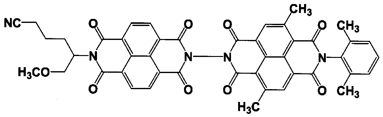
- Second step Synthesis of naphthalene monoimide monohydrazone derivative (1-2)
- a reactor charged with 3.0 g of the naphthalene monoimide derivative (1-1), 2.0 g of the naphthalene monoimide monohydrazone derivative (1-2), and 50 ml of dehydrated DMI was reacted at 190 ° C. for 22 hours. After cooling, extraction was performed, and the organic layer was concentrated to obtain a solid.
- the melting point was measured to be 210.9 ° C.
- naphthalene monoimide compound (2-1) obtained above and dehydrated DMF100 ml were charged and dissolved.
- 1.65 g of hydrazine 'monohydrate was added dropwise over 2 minutes, and reacted at room temperature for 1.5 hours.
- the precipitated crystals were filtered, washed with methanol, and dried to obtain a naphthalene monoimide monohydrazone derivative (2-2). Yield: 8.27 g.
- a film was formed to a thickness of 300 nm by a sputtering method, and this was used as an insulator layer.
- the substrate thus dried was attached to a temperature-controllable substrate holder in a vacuum evaporation apparatus. Then, the mask for the organic compound layer is attached in a vacuum, and the hole transport layer (TPD) is first heated to 600 mm by the heat of the carbon crucible. A layer of aluminum alloy, Alq3) was deposited in the order of 400A, and an electron injection / transport layer (exemplified compound (8)) was deposited in the order of 200A.
- TPD hole transport layer
- a glass substrate manufactured by HOYA Co., Ltd.
- ITO 1000 A force S patterning to become a transparent electrode
- the substrate is ultrasonically cleaned in the order of acetone, deionized water, a substrate cleaning agent (Semicoclean EL grade, manufactured by Flu Chemical), deionized water, and isopropyl alcohol (IPA), then pulled up from boiling IPA and dried. did.
- UV ozone treatment was performed to remove organic contaminants on the ITO surface.
Landscapes
- Physics & Mathematics (AREA)
- Chemical & Material Sciences (AREA)
- General Physics & Mathematics (AREA)
- Engineering & Computer Science (AREA)
- Organic Chemistry (AREA)
- Spectroscopy & Molecular Physics (AREA)
- Materials Engineering (AREA)
- Nanotechnology (AREA)
- Theoretical Computer Science (AREA)
- Crystallography & Structural Chemistry (AREA)
- Mathematical Physics (AREA)
- Optics & Photonics (AREA)
- Electromagnetism (AREA)
- Electroluminescent Light Sources (AREA)
- Photoreceptors In Electrophotography (AREA)
- Nitrogen And Oxygen Or Sulfur-Condensed Heterocyclic Ring Systems (AREA)
- Thin Film Transistor (AREA)
- Heterocyclic Carbon Compounds Containing A Hetero Ring Having Oxygen Or Sulfur (AREA)
Description


Claims


Priority Applications (4)
| Application Number | Priority Date | Filing Date | Title |
|---|---|---|---|
| US10/594,156 US7763727B2 (en) | 2004-03-29 | 2005-03-29 | Compound and organic electronic device using the same |
| CN200580010086.5A CN1938321B (zh) | 2004-03-29 | 2005-03-29 | 新型化合物及使用该化合物的有机电子元件 |
| JP2006511588A JP4627528B2 (ja) | 2004-03-29 | 2005-03-29 | 新規化合物、および該化合物を用いた有機エレクトロニクス素子 |
| EP05727671A EP1736476A4 (en) | 2004-03-29 | 2005-03-29 | NEW CONNECTION AND ORGANIC ELECTRONIC DEVICE USING SUCH A CONNECTION |
Applications Claiming Priority (6)
| Application Number | Priority Date | Filing Date | Title |
|---|---|---|---|
| JP2004-094088 | 2004-03-29 | ||
| JP2004094088 | 2004-03-29 | ||
| JP2004-277461 | 2004-09-24 | ||
| JP2004277461 | 2004-09-24 | ||
| JP2004351088 | 2004-12-03 | ||
| JP2004-351088 | 2004-12-03 |
Publications (1)
| Publication Number | Publication Date |
|---|---|
| WO2005092901A1 true WO2005092901A1 (ja) | 2005-10-06 |
Family
ID=35056132
Family Applications (1)
| Application Number | Title | Priority Date | Filing Date |
|---|---|---|---|
| PCT/JP2005/005979 Ceased WO2005092901A1 (ja) | 2004-03-29 | 2005-03-29 | 新規化合物、および該化合物を用いた有機エレクトロニクス素子 |
Country Status (6)
| Country | Link |
|---|---|
| US (1) | US7763727B2 (ja) |
| EP (1) | EP1736476A4 (ja) |
| JP (1) | JP4627528B2 (ja) |
| KR (1) | KR100861434B1 (ja) |
| CN (1) | CN1938321B (ja) |
| WO (1) | WO2005092901A1 (ja) |
Cited By (83)
| Publication number | Priority date | Publication date | Assignee | Title |
|---|---|---|---|---|
| JP2007094360A (ja) * | 2005-09-02 | 2007-04-12 | Ricoh Co Ltd | 電子写真装置 |
| JP2007108719A (ja) * | 2005-09-15 | 2007-04-26 | Ricoh Co Ltd | 電子写真感光体、画像形成装置、フルカラー画像形成装置、及びプロセスカートリッジ |
| JP2007108665A (ja) * | 2005-09-15 | 2007-04-26 | Ricoh Co Ltd | 電子写真感光体、画像形成装置、フルカラー画像形成装置及びプロセスカートリッジ |
| JP2007108645A (ja) * | 2005-09-16 | 2007-04-26 | Ricoh Co Ltd | 画像形成装置及びプロセスカートリッジ |
| JP2007108667A (ja) * | 2005-09-14 | 2007-04-26 | Ricoh Co Ltd | プロセスカートリッジ及び画像形成装置 |
| JP2007108647A (ja) * | 2005-09-15 | 2007-04-26 | Ricoh Co Ltd | 電子写真装置 |
| JP2007108644A (ja) * | 2005-09-15 | 2007-04-26 | Ricoh Co Ltd | 画像形成装置及びプロセスカートリッジ |
| JP2007108633A (ja) * | 2005-09-13 | 2007-04-26 | Ricoh Co Ltd | 電子写真装置 |
| JP2007108646A (ja) * | 2005-09-15 | 2007-04-26 | Ricoh Co Ltd | 電子写真装置 |
| JP2007108632A (ja) * | 2005-09-14 | 2007-04-26 | Ricoh Co Ltd | 電子写真装置 |
| JP2007108651A (ja) * | 2005-09-16 | 2007-04-26 | Ricoh Co Ltd | 感光体、画像形成装置及びプロセスカートリッジ |
| JP2007108650A (ja) * | 2005-09-15 | 2007-04-26 | Ricoh Co Ltd | 画像形成装置、画像形成方法及びプロセスカートリッジ |
| JP2007108637A (ja) * | 2005-09-13 | 2007-04-26 | Ricoh Co Ltd | 電子写真装置 |
| JP2007108658A (ja) * | 2005-09-16 | 2007-04-26 | Ricoh Co Ltd | 画像形成装置及び画像形成装置用プロセスカートリッジ |
| JP2007108682A (ja) * | 2005-09-15 | 2007-04-26 | Ricoh Co Ltd | 画像形成装置 |
| JP2007108643A (ja) * | 2005-09-16 | 2007-04-26 | Ricoh Co Ltd | 画像形成装置及びプロセスカートリッジ |
| JP2007108652A (ja) * | 2005-09-16 | 2007-04-26 | Ricoh Co Ltd | 画像形成装置及びプロセスカートリッジ |
| JP2007108659A (ja) * | 2005-09-15 | 2007-04-26 | Ricoh Co Ltd | 電子写真感光体および電子写真装置 |
| JP2007108636A (ja) * | 2005-09-15 | 2007-04-26 | Ricoh Co Ltd | 電子写真装置、電子写真方法及びプロセスカートリッジ |
| JP2007108649A (ja) * | 2005-09-16 | 2007-04-26 | Ricoh Co Ltd | プロセスカートリッジ、画像形成装置及び画像形成方法 |
| JP2007108670A (ja) * | 2005-09-15 | 2007-04-26 | Ricoh Co Ltd | 電子写真感光体、画像形成装置、フルカラー画像形成装置及びプロセスカートリッジ |
| JP2007108671A (ja) * | 2005-09-15 | 2007-04-26 | Ricoh Co Ltd | 電子写真感光体、画像形成装置及びプロセスカートリッジ |
| JP2007187728A (ja) * | 2006-01-11 | 2007-07-26 | Canon Inc | 電子写真感光体、プロセスカートリッジ及び電子写真装置 |
| JP2007219126A (ja) * | 2006-02-16 | 2007-08-30 | Ricoh Co Ltd | 画像形成装置 |
| JP2007233116A (ja) * | 2006-03-02 | 2007-09-13 | Ricoh Co Ltd | 電子写真感光体、画像形成装置及びプロセスカートリッジ |
| JP2007264589A (ja) * | 2005-09-15 | 2007-10-11 | Ricoh Co Ltd | 画像形成方法及び画像形成装置 |
| EP1847882A1 (en) * | 2006-04-20 | 2007-10-24 | Ricoh Company, Ltd. | Electrophotographic photoconductor, image forming apparatus, and process cartridge |
| JP2007286536A (ja) * | 2006-04-20 | 2007-11-01 | Ricoh Co Ltd | 電子写真感光体、画像形成装置及びプロセスカートリッジ |
| JP2007304365A (ja) * | 2006-05-12 | 2007-11-22 | Ricoh Co Ltd | 画像形成装置 |
| JP2007322576A (ja) * | 2006-05-31 | 2007-12-13 | Ricoh Co Ltd | 電子写真感光体、画像形成装置、プロセスカートリッジ |
| JP2008033207A (ja) * | 2005-09-15 | 2008-02-14 | Ricoh Co Ltd | 電子写真感光体、画像形成装置、フルカラー画像形成装置及びプロセスカートリッジ |
| JP2008052014A (ja) * | 2006-08-24 | 2008-03-06 | Ricoh Co Ltd | 電子写真感光体、画像形成装置及びプロセスカートリッジ |
| JP2008065115A (ja) * | 2006-09-08 | 2008-03-21 | Ricoh Co Ltd | 画像形成装置 |
| JP2008122740A (ja) * | 2006-11-14 | 2008-05-29 | Ricoh Co Ltd | 電子写真感光体、画像形成装置及びプロセスカートリッジ |
| JP2008122763A (ja) * | 2006-11-14 | 2008-05-29 | Ricoh Co Ltd | 画像形成装置 |
| JP2008216713A (ja) * | 2007-03-06 | 2008-09-18 | Ricoh Co Ltd | 画像形成方法及び画像形成装置 |
| JP2008224785A (ja) * | 2007-03-09 | 2008-09-25 | Ricoh Co Ltd | 画像形成装置及びプロセスカートリッジ |
| JP2008281800A (ja) * | 2007-05-11 | 2008-11-20 | Ricoh Co Ltd | 電子写真感光体、画像形成装置及びプロセスカートリッジ |
| JP2008281805A (ja) * | 2007-05-11 | 2008-11-20 | Ricoh Co Ltd | 画像形成装置及び画像形成装置用プロセスカートリッジ |
| WO2009005669A3 (en) * | 2007-06-29 | 2009-03-12 | Eastman Kodak Co | Tetracarboxylic diimide semiconductor for thin film transistors |
| WO2008051552A3 (en) * | 2006-10-25 | 2009-03-19 | Univ Northwestern | Organic semiconductor materials and methods of preparing and use thereof |
| JP2009099941A (ja) * | 2007-09-28 | 2009-05-07 | Fujifilm Corp | 放射線検出器、放射線検出器の製造方法、塗布液及び有機高分子層の製造方法 |
| US7569693B2 (en) | 2006-06-12 | 2009-08-04 | Northwestern University | Naphthalene-based semiconductor materials and methods of preparing and use thereof |
| JP2009292802A (ja) * | 2007-09-10 | 2009-12-17 | Ricoh Co Ltd | ナフタレンテトラカルボン酸ジイミド誘導体、及び該ナフタレンテトラカルボン酸ジイミド誘導体を用いた電子写真感光体 |
| US7671202B2 (en) | 2004-01-26 | 2010-03-02 | Northwestern University | Perylene n-type semiconductors and related devices |
| US7747197B2 (en) * | 2005-09-13 | 2010-06-29 | Ricoh Company, Ltd. | Electrophotographic image forming apparatus and process cartridge |
| JP2010254608A (ja) * | 2009-04-23 | 2010-11-11 | Idemitsu Kosan Co Ltd | フタルイミド系化合物、ナフタルイミド系化合物、無水ナフタル酸系化合物、これら含む電子輸送材料、及び有機薄膜太陽電池 |
| JP2010537427A (ja) * | 2007-08-23 | 2010-12-02 | エスアールアイ インターナショナル | 有機カソードを用いるエレクトロルミネッセントデバイス |
| US7871747B2 (en) * | 2005-09-13 | 2011-01-18 | Ricoh Company, Ltd. | Electrophotographic photoconductor having charge blocking and moire preventing layers |
| US7893265B2 (en) | 2007-01-08 | 2011-02-22 | Polyera Corporation | Methods for preparing arene-BIS (dicarboximide)-based semiconducting materials and related intermediates for preparing same |
| US7902363B2 (en) | 2006-11-17 | 2011-03-08 | Polyera Corporation | Diimide-based semiconductor materials and methods of preparing and using the same |
| US8007972B2 (en) * | 2005-09-15 | 2011-08-30 | Ricoh Company, Ltd. | Electrophotographic photoconductor, and image forming apparatus, process cartridge and image forming method using the same |
| JP2011524862A (ja) * | 2008-05-30 | 2011-09-08 | ビーエーエスエフ ソシエタス・ヨーロピア | 半導体材料並びにその製造方法およびその使用 |
| US8022214B2 (en) | 2007-01-24 | 2011-09-20 | Polyera Corporation | Organic semiconductor materials and precursors thereof |
| JP2013032296A (ja) * | 2011-08-01 | 2013-02-14 | Ricoh Co Ltd | ビスジアザペンタジエン誘導体およびそれらの製造方法 |
| JP2014224987A (ja) * | 2013-04-25 | 2014-12-04 | キヤノン株式会社 | 電子写真感光体、プロセスカートリッジ、電子写真装置およびイミド化合物 |
| US9266892B2 (en) | 2012-12-19 | 2016-02-23 | Incyte Holdings Corporation | Fused pyrazoles as FGFR inhibitors |
| US9388185B2 (en) | 2012-08-10 | 2016-07-12 | Incyte Holdings Corporation | Substituted pyrrolo[2,3-b]pyrazines as FGFR inhibitors |
| US9533984B2 (en) | 2013-04-19 | 2017-01-03 | Incyte Holdings Corporation | Bicyclic heterocycles as FGFR inhibitors |
| US9533954B2 (en) | 2010-12-22 | 2017-01-03 | Incyte Corporation | Substituted imidazopyridazines and benzimidazoles as inhibitors of FGFR3 |
| US9580423B2 (en) | 2015-02-20 | 2017-02-28 | Incyte Corporation | Bicyclic heterocycles as FGFR4 inhibitors |
| US9611267B2 (en) | 2012-06-13 | 2017-04-04 | Incyte Holdings Corporation | Substituted tricyclic compounds as FGFR inhibitors |
| US9708318B2 (en) | 2015-02-20 | 2017-07-18 | Incyte Corporation | Bicyclic heterocycles as FGFR4 inhibitors |
| US9890156B2 (en) | 2015-02-20 | 2018-02-13 | Incyte Corporation | Bicyclic heterocycles as FGFR4 inhibitors |
| US10611762B2 (en) | 2017-05-26 | 2020-04-07 | Incyte Corporation | Crystalline forms of a FGFR inhibitor and processes for preparing the same |
| US10851105B2 (en) | 2014-10-22 | 2020-12-01 | Incyte Corporation | Bicyclic heterocycles as FGFR4 inhibitors |
| US11174257B2 (en) | 2018-05-04 | 2021-11-16 | Incyte Corporation | Salts of an FGFR inhibitor |
| US11407750B2 (en) | 2019-12-04 | 2022-08-09 | Incyte Corporation | Derivatives of an FGFR inhibitor |
| US11466004B2 (en) | 2018-05-04 | 2022-10-11 | Incyte Corporation | Solid forms of an FGFR inhibitor and processes for preparing the same |
| US11566028B2 (en) | 2019-10-16 | 2023-01-31 | Incyte Corporation | Bicyclic heterocycles as FGFR inhibitors |
| US11591329B2 (en) | 2019-07-09 | 2023-02-28 | Incyte Corporation | Bicyclic heterocycles as FGFR inhibitors |
| US11607416B2 (en) | 2019-10-14 | 2023-03-21 | Incyte Corporation | Bicyclic heterocycles as FGFR inhibitors |
| US11628162B2 (en) | 2019-03-08 | 2023-04-18 | Incyte Corporation | Methods of treating cancer with an FGFR inhibitor |
| US11897891B2 (en) | 2019-12-04 | 2024-02-13 | Incyte Corporation | Tricyclic heterocycles as FGFR inhibitors |
| US11939331B2 (en) | 2021-06-09 | 2024-03-26 | Incyte Corporation | Tricyclic heterocycles as FGFR inhibitors |
| US12012409B2 (en) | 2020-01-15 | 2024-06-18 | Incyte Corporation | Bicyclic heterocycles as FGFR inhibitors |
| US12065494B2 (en) | 2021-04-12 | 2024-08-20 | Incyte Corporation | Combination therapy comprising an FGFR inhibitor and a Nectin-4 targeting agent |
| US12122767B2 (en) | 2019-10-01 | 2024-10-22 | Incyte Corporation | Bicyclic heterocycles as FGFR inhibitors |
| WO2025004567A1 (ja) * | 2023-06-26 | 2025-01-02 | 東ソー株式会社 | 有機電子素子、及び化合物 |
| WO2025022986A1 (ja) * | 2023-07-24 | 2025-01-30 | 東ソー株式会社 | 有機電子素子、有機電子素子用材料及びイミド化合物 |
| EP4528382A1 (en) * | 2023-09-25 | 2025-03-26 | FUJIFILM Business Innovation Corp. | Electrophotographic photoreceptor, process cartridge, and image forming apparatus |
| US12428420B2 (en) | 2021-06-09 | 2025-09-30 | Incyte Corporation | Tricyclic heterocycles as FGFR inhibitors |
| WO2026058896A1 (ja) * | 2024-09-11 | 2026-03-19 | 東ソー株式会社 | 有機電子素子、有機電子素子用材料及びイミド化合物 |
Families Citing this family (34)
| Publication number | Priority date | Publication date | Assignee | Title |
|---|---|---|---|---|
| US20070018153A1 (en) * | 2005-07-20 | 2007-01-25 | Osram-Opto Semiconductors Gmbh | Thick light emitting polymers to enhance oled efficiency and lifetime |
| DE102005053995A1 (de) * | 2005-11-10 | 2007-05-24 | Basf Ag | Verwendung von Rylenderivaten als Photosensibilisatoren in Solarzellen |
| KR101221761B1 (ko) * | 2006-12-01 | 2013-01-11 | 삼성전자주식회사 | 유기 반도체 물질의 산화 및 선택적 환원을 이용한 고성능유기 박막 트랜지스터의 제조방법 |
| US8110326B2 (en) | 2007-06-04 | 2012-02-07 | Ricoh Company Limited | Electrophotographic photoreceptor, image forming apparatus, and process cartridge |
| JP5168478B2 (ja) * | 2007-06-04 | 2013-03-21 | 株式会社リコー | 電子写真感光体、電子写真方法、電子写真装置、並びに電子写真装置用プロセスカートリッジ |
| CN101689606B (zh) * | 2007-07-10 | 2012-02-08 | 巴斯夫欧洲公司 | 用于生产有机太阳能电池和有机光检测器光敏层的混合物 |
| US7906724B2 (en) | 2007-07-31 | 2011-03-15 | Agency For Science, Technology And Research | N-type conjugated materials based on 2-vinyl-4,5-dicyanoimidazoles and their use in organic photovoltaics |
| US8380109B2 (en) * | 2008-01-11 | 2013-02-19 | Ricoh Company, Ltd. | Image forming apparatus and process cartridge |
| TWI478624B (zh) * | 2008-03-27 | 2015-03-21 | Nippon Steel & Sumikin Chem Co | Organic electroluminescent elements |
| US20120211063A1 (en) * | 2009-03-17 | 2012-08-23 | Jong-Jan Lee | Back Contact Solar Cell with Organic Semiconductor Heterojunctions |
| CN101508893B (zh) * | 2009-03-23 | 2012-10-03 | 安徽大学 | 1,4,5,8-萘四甲酸二酰亚胺衍生物双荧光材料及其制备方法 |
| KR101249686B1 (ko) * | 2009-07-16 | 2013-04-05 | 주식회사 엘지화학 | 폴리이미드 및 이를 포함하는 감광성 수지 조성물 |
| TW201123578A (en) * | 2009-07-27 | 2011-07-01 | Univ Michigan | Bulk heterojunction organic photovoltaic cells made by glancing angle deposition |
| WO2011082234A1 (en) | 2009-12-29 | 2011-07-07 | Polyera Corporation | Thionated aromatic bisimides as organic semiconductors and devices incorporating them |
| WO2011127475A1 (en) * | 2010-04-09 | 2011-10-13 | The Arizona Board Of Regents On Behalf Of The University Of Arizona | Organic photovoltaic devices comprising solution- processed substituted metal-phthalocyanines and exhibiting near-ir photo-sensitivity |
| JP5479228B2 (ja) * | 2010-05-28 | 2014-04-23 | 三洋電機株式会社 | 太陽電池モジュール |
| KR101117127B1 (ko) * | 2010-08-06 | 2012-02-24 | 한국과학기술연구원 | 비정질 실리콘 태양전지와 유기 태양전지를 이용한 탠덤형 태양전지 |
| WO2012106119A1 (en) * | 2011-02-03 | 2012-08-09 | Konarka Technologies, Inc. | Photovoltaic cells |
| US8921553B2 (en) | 2011-04-15 | 2014-12-30 | Georgia Tech Research-Corporation | Stannyl derivatives of naphthalene diimides and related compositions and methods |
| US20130263925A1 (en) * | 2012-04-05 | 2013-10-10 | Merck Patent Gmbh | Hole Carrier Layer For Organic Photovoltaic Device |
| US9276157B2 (en) * | 2012-08-31 | 2016-03-01 | First Solar, Inc. | Methods of treating a semiconductor layer |
| ES2471568B1 (es) * | 2012-11-22 | 2015-08-21 | Abengoa Solar New Technologies S.A. | Procedimiento para la creación de contactos eléctricos y contactos así creados |
| US20140174496A1 (en) * | 2012-12-21 | 2014-06-26 | Georgia Tech Research Corporation | Hybrid generator using thermoelectric generation and piezoelectric generation |
| US20140203259A1 (en) * | 2013-01-18 | 2014-07-24 | Universal Display Corporation | Host for organic light emitting devices |
| CN104078594A (zh) * | 2013-03-27 | 2014-10-01 | 海洋王照明科技股份有限公司 | 一种有机电致发光器件及其制备方法 |
| CN104051671B (zh) * | 2014-06-16 | 2016-03-16 | 京东方科技集团股份有限公司 | 一种oled显示装置及其制备方法 |
| CN107430359B (zh) * | 2015-04-03 | 2021-08-03 | 京瓷办公信息系统株式会社 | 带正电单层型电子照相感光体、处理盒和图像形成装置 |
| US9711350B2 (en) | 2015-06-03 | 2017-07-18 | Asm Ip Holding B.V. | Methods for semiconductor passivation by nitridation |
| CN105655480A (zh) * | 2016-01-04 | 2016-06-08 | 京东方科技集团股份有限公司 | 一种压电薄膜传感器、压电薄膜传感器电路及制作方法 |
| US10903438B2 (en) * | 2017-06-16 | 2021-01-26 | Ubiquitous Energy, Inc. | Visibly transparent, ultraviolet-absorbing photovoltaic devices |
| US11778896B2 (en) | 2017-06-16 | 2023-10-03 | Ubiquitous Energy, Inc. | Visibly transparent, near-infrared-absorbing metal-complex photovoltaic devices |
| US11545635B2 (en) | 2017-06-16 | 2023-01-03 | Ubiquitous Energy, Inc. | Visibly transparent, near-infrared-absorbing boron-containing photovoltaic devices |
| CN112286016B (zh) * | 2019-07-22 | 2023-08-25 | 广东乐普泰新材料科技有限公司 | 一种单层正电性有机感光鼓及其制备方法 |
| WO2021171604A1 (ja) * | 2020-02-28 | 2021-09-02 | シャープ株式会社 | 表示装置及び表示装置の製造方法 |
Citations (10)
| Publication number | Priority date | Publication date | Assignee | Title |
|---|---|---|---|---|
| JPH05148812A (ja) * | 1991-11-29 | 1993-06-15 | Nippon Samikon Kk | ロードヒーテイング用プレキヤストコンクリート舗装版 |
| US5645965A (en) | 1996-08-08 | 1997-07-08 | Xerox Corporation | Symmetrical perylene dimers |
| JPH11124382A (ja) | 1997-07-24 | 1999-05-11 | Ciba Specialty Chem Holding Inc | カルボニル化合物の蛍光誘導体化−新規なカルボニル試薬 |
| JPH11212283A (ja) * | 1998-01-26 | 1999-08-06 | Konica Corp | 電子写真感光体 |
| US6051351A (en) | 1999-05-21 | 2000-04-18 | Xerox Corporation | Perylenes |
| JP2000214611A (ja) * | 1999-01-25 | 2000-08-04 | Kyocera Mita Corp | 電子写真感光体 |
| JP2004093803A (ja) * | 2002-08-30 | 2004-03-25 | Canon Inc | 電子写真感光体、プロセスカートリッジおよび電子写真装置 |
| JP2004093791A (ja) * | 2002-08-30 | 2004-03-25 | Canon Inc | ナフタレンアミジンイミド化合物、ナフタレンアミジンイミド化合物を含有する電子写真感光体、該電子写真感光体を有するプロセスカートリッジおよび電子写真装置 |
| JP2005126367A (ja) * | 2003-10-23 | 2005-05-19 | Mitsui Chemicals Inc | ナフタレンカルボン酸誘導体、および該化合物を用いた電子写真感光体、電子写真装置 |
| JP2005154409A (ja) * | 2003-07-16 | 2005-06-16 | Mitsui Chemicals Inc | 新規なナフタレンカルボン酸誘導体、および該化合物を用いた電子写真感光体、電子写真装置 |
Family Cites Families (5)
| Publication number | Priority date | Publication date | Assignee | Title |
|---|---|---|---|---|
| JP2718048B2 (ja) | 1988-02-15 | 1998-02-25 | 株式会社ブリヂストン | 電子写真感光体用電荷輸送剤及び電子写真感光体 |
| JP2922212B2 (ja) | 1989-02-17 | 1999-07-19 | パイオニア株式会社 | 電界発光素子 |
| JPH05142812A (ja) | 1991-11-16 | 1993-06-11 | Kao Corp | 電子写真感光体 |
| JP2001052204A (ja) | 1999-08-10 | 2001-02-23 | Monorisu:Kk | オブジェクト符号化方法、復号方法およびそれらの方法を利用可能な装置 |
| JP4078113B2 (ja) * | 2002-05-10 | 2008-04-23 | キヤノン株式会社 | ナフタレンテトラカルボン酸ジイミド化合物の製造方法 |
-
2005
- 2005-03-29 US US10/594,156 patent/US7763727B2/en not_active Expired - Fee Related
- 2005-03-29 KR KR1020067021674A patent/KR100861434B1/ko not_active Expired - Fee Related
- 2005-03-29 EP EP05727671A patent/EP1736476A4/en not_active Withdrawn
- 2005-03-29 JP JP2006511588A patent/JP4627528B2/ja not_active Expired - Fee Related
- 2005-03-29 CN CN200580010086.5A patent/CN1938321B/zh not_active Expired - Fee Related
- 2005-03-29 WO PCT/JP2005/005979 patent/WO2005092901A1/ja not_active Ceased
Patent Citations (13)
| Publication number | Priority date | Publication date | Assignee | Title |
|---|---|---|---|---|
| JPH05148812A (ja) * | 1991-11-29 | 1993-06-15 | Nippon Samikon Kk | ロードヒーテイング用プレキヤストコンクリート舗装版 |
| US5645965A (en) | 1996-08-08 | 1997-07-08 | Xerox Corporation | Symmetrical perylene dimers |
| JPH10133403A (ja) | 1996-08-08 | 1998-05-22 | Xerox Corp | 対称ペリレンダイマー |
| US6060601A (en) | 1997-07-24 | 2000-05-09 | Ciba Specialty Chemicals Corporation | Fluorescence-derivatisation of carbonyl compounds-novel carbonyl reagents |
| JPH11124382A (ja) | 1997-07-24 | 1999-05-11 | Ciba Specialty Chem Holding Inc | カルボニル化合物の蛍光誘導体化−新規なカルボニル試薬 |
| JPH11212283A (ja) * | 1998-01-26 | 1999-08-06 | Konica Corp | 電子写真感光体 |
| JP2000214611A (ja) * | 1999-01-25 | 2000-08-04 | Kyocera Mita Corp | 電子写真感光体 |
| US6051351A (en) | 1999-05-21 | 2000-04-18 | Xerox Corporation | Perylenes |
| JP2001005204A (ja) | 1999-05-21 | 2001-01-12 | Xerox Corp | 光導電性画像形成部材 |
| JP2004093803A (ja) * | 2002-08-30 | 2004-03-25 | Canon Inc | 電子写真感光体、プロセスカートリッジおよび電子写真装置 |
| JP2004093791A (ja) * | 2002-08-30 | 2004-03-25 | Canon Inc | ナフタレンアミジンイミド化合物、ナフタレンアミジンイミド化合物を含有する電子写真感光体、該電子写真感光体を有するプロセスカートリッジおよび電子写真装置 |
| JP2005154409A (ja) * | 2003-07-16 | 2005-06-16 | Mitsui Chemicals Inc | 新規なナフタレンカルボン酸誘導体、および該化合物を用いた電子写真感光体、電子写真装置 |
| JP2005126367A (ja) * | 2003-10-23 | 2005-05-19 | Mitsui Chemicals Inc | ナフタレンカルボン酸誘導体、および該化合物を用いた電子写真感光体、電子写真装置 |
Non-Patent Citations (20)
| Title |
|---|
| DEBRECZENY ET AL., J. AM. CHEM. SOC., vol. 118, 1996, pages 8174 - 8175 |
| DEBRECZENY M. ET AL: "Femtosecond Optical Control of Charge Shift within Electron Donor-Acceptor Arrays: An Approach to Molecular Swithches.", JOURNAL OF HTE AMERICAN CHEMICAL SOCIETY., vol. 118, no. 34, 28 August 1996 (1996-08-28), pages 8174 - 8175, XP002990120 * |
| DINE-HART ET AL., DIE MAKROMOLECULARE CHEMIE, vol. 153, 1972, pages 237 - 54 |
| DINE-HART R.A. ET AL: "Effect of structural variations on the thermooxidative stability of aromatic polymides.", MEKROMOLEKULARE CHEMIE., vol. 153, 14 March 1972 (1972-03-14), pages 237 - 54, XP002990124 * |
| GIAIMO ET AL., J. AM. CHEM. SOC., vol. 124, 2002, pages 8530 - 8531 |
| GIAIMO J. ET AL: "Excited-state symmetry breaking in cofacial and linear dimers of a green perylenediimide chlorophyll analogue leading to ultrafast charge separation.", JOURNAL OF THE EMERICAN CHEMICAL SOCIETY., vol. 124, no. 29, 24 July 2002 (2002-07-24), pages 8530 - 8531, XP002990118 * |
| HEINEN ET AL., J. PHYS. CHEM. A, vol. 106, 2002, pages 1933 - 1937 |
| HEINEN U. ET AL: "High Time Resolution Q-Band EPR Study of Sequential Electron Transfer in a Triad Oriented in a Liquid Crystal.", JOURNAL OF PHYSICAL CHEMISTRY A., vol. 106, no. 10, 14 March 2002 (2002-03-14), pages 1933 - 1937, XP002990122 * |
| LANGHALS H. ET AL: "Intense dyes through chromophore-chromophore interactions: bi- and trichromophoric perylene-3,4:9,10-bis(dicarboximide)s.", ANGEWANDTE CHEMIE, INTERNATIONAL EDITION., vol. 37, no. 7, 20 April 1998 (1998-04-20), pages 952 - 955, XP000931227 * |
| LUKAS A. ET AL: "Biomimetic electron transfer using low energy excited states: A green perylene-based analogue of chlorophylla.", JOURNAL OF PHYSICAL CHEMISTRY., vol. 106, no. 6, 14 February 2002 (2002-02-14), pages 1299 - 1306, XP002990117 * |
| LUKAS A. ET AL: "Femtosecond Optical Switching of Electron Transport Direction in Branched Donor-Acceptor Arrays.", JOURNAL OF PHYSICAL CHEMISTRY B., vol. 104, no. 5, 10 February 2000 (2000-02-10), pages 931 - 940, XP002990121 * |
| LUKAS ET AL., J. PHYS. CHEM. B, vol. 104, 2000, pages 931 - 940 |
| LUKAS ET AL., J. PHYS. CHEM. B, vol. 106, 2002, pages 1299 - 1306 |
| MILLER ET AL., CHEMICAL PHYSICS, vol. 275, 2002, pages 167 - 183 |
| MILLER S. ET AL: "Ultrafast electron transfer reactions initiated by excited CT states of push-pull perylenes.", CHEMICAL PHYSICS., vol. 275, no. 1-3, 1 January 2002 (2002-01-01), pages 167 - 183, XP002990119 * |
| MORI ET AL., J. PHYS. CHEM. A, vol. 106, 2002, pages 4453 - 4467 |
| MORI Y. ET AL: "Spin effects on decay dynamics of charge-separeted states generated by photoinduced electron transfer in zinc porphyrin-naphthalenediimide dyads.", JOURNAL OF PHYSICAL CHEMISTRY., vol. 106, no. 18, 9 May 2002 (2002-05-09), pages 4453 - 4467, XP002971037 * |
| OKAMOTO ET AL., CHEM. EUR. J., vol. 10, 2004, pages 474 - 483 |
| OKAMOTO K. ET AL: "Effects of metal ions on photoinduced electron transfer in zinc prophyrin-naphthalenediimide linked systems.", CHEMISTRY--A EUROPEAN JOURNAL., vol. 10, no. 2, 23 January 2004 (2004-01-23), pages 474 - 483, XP002990123 * |
| See also references of EP1736476A4 |
Cited By (120)
| Publication number | Priority date | Publication date | Assignee | Title |
|---|---|---|---|---|
| US7982039B2 (en) | 2004-01-26 | 2011-07-19 | Northwestern University | N-type semiconductors and related devices |
| US7671202B2 (en) | 2004-01-26 | 2010-03-02 | Northwestern University | Perylene n-type semiconductors and related devices |
| JP2007094360A (ja) * | 2005-09-02 | 2007-04-12 | Ricoh Co Ltd | 電子写真装置 |
| JP2007108637A (ja) * | 2005-09-13 | 2007-04-26 | Ricoh Co Ltd | 電子写真装置 |
| US7747197B2 (en) * | 2005-09-13 | 2010-06-29 | Ricoh Company, Ltd. | Electrophotographic image forming apparatus and process cartridge |
| US7871747B2 (en) * | 2005-09-13 | 2011-01-18 | Ricoh Company, Ltd. | Electrophotographic photoconductor having charge blocking and moire preventing layers |
| US8064795B2 (en) | 2005-09-13 | 2011-11-22 | Ricoh Company, Ltd. | Electrophotographic image forming apparatus and process cartridge |
| US8227156B2 (en) | 2005-09-13 | 2012-07-24 | Ricoh Company, Ltd. | Electrophotographic photoconductor, image forming apparatus, image forming method, and process cartridge |
| JP2007108633A (ja) * | 2005-09-13 | 2007-04-26 | Ricoh Co Ltd | 電子写真装置 |
| JP2007108667A (ja) * | 2005-09-14 | 2007-04-26 | Ricoh Co Ltd | プロセスカートリッジ及び画像形成装置 |
| JP2007108632A (ja) * | 2005-09-14 | 2007-04-26 | Ricoh Co Ltd | 電子写真装置 |
| JP2007108636A (ja) * | 2005-09-15 | 2007-04-26 | Ricoh Co Ltd | 電子写真装置、電子写真方法及びプロセスカートリッジ |
| JP2007264589A (ja) * | 2005-09-15 | 2007-10-11 | Ricoh Co Ltd | 画像形成方法及び画像形成装置 |
| JP2007108719A (ja) * | 2005-09-15 | 2007-04-26 | Ricoh Co Ltd | 電子写真感光体、画像形成装置、フルカラー画像形成装置、及びプロセスカートリッジ |
| JP2007108682A (ja) * | 2005-09-15 | 2007-04-26 | Ricoh Co Ltd | 画像形成装置 |
| JP2007108665A (ja) * | 2005-09-15 | 2007-04-26 | Ricoh Co Ltd | 電子写真感光体、画像形成装置、フルカラー画像形成装置及びプロセスカートリッジ |
| US8007972B2 (en) * | 2005-09-15 | 2011-08-30 | Ricoh Company, Ltd. | Electrophotographic photoconductor, and image forming apparatus, process cartridge and image forming method using the same |
| JP2007108659A (ja) * | 2005-09-15 | 2007-04-26 | Ricoh Co Ltd | 電子写真感光体および電子写真装置 |
| JP2007108650A (ja) * | 2005-09-15 | 2007-04-26 | Ricoh Co Ltd | 画像形成装置、画像形成方法及びプロセスカートリッジ |
| JP2007108647A (ja) * | 2005-09-15 | 2007-04-26 | Ricoh Co Ltd | 電子写真装置 |
| JP2007108670A (ja) * | 2005-09-15 | 2007-04-26 | Ricoh Co Ltd | 電子写真感光体、画像形成装置、フルカラー画像形成装置及びプロセスカートリッジ |
| JP2007108671A (ja) * | 2005-09-15 | 2007-04-26 | Ricoh Co Ltd | 電子写真感光体、画像形成装置及びプロセスカートリッジ |
| JP2007108644A (ja) * | 2005-09-15 | 2007-04-26 | Ricoh Co Ltd | 画像形成装置及びプロセスカートリッジ |
| JP2008033207A (ja) * | 2005-09-15 | 2008-02-14 | Ricoh Co Ltd | 電子写真感光体、画像形成装置、フルカラー画像形成装置及びプロセスカートリッジ |
| JP2007108646A (ja) * | 2005-09-15 | 2007-04-26 | Ricoh Co Ltd | 電子写真装置 |
| JP2007108651A (ja) * | 2005-09-16 | 2007-04-26 | Ricoh Co Ltd | 感光体、画像形成装置及びプロセスカートリッジ |
| JP2007108649A (ja) * | 2005-09-16 | 2007-04-26 | Ricoh Co Ltd | プロセスカートリッジ、画像形成装置及び画像形成方法 |
| JP2007108658A (ja) * | 2005-09-16 | 2007-04-26 | Ricoh Co Ltd | 画像形成装置及び画像形成装置用プロセスカートリッジ |
| JP2007108643A (ja) * | 2005-09-16 | 2007-04-26 | Ricoh Co Ltd | 画像形成装置及びプロセスカートリッジ |
| JP2007108645A (ja) * | 2005-09-16 | 2007-04-26 | Ricoh Co Ltd | 画像形成装置及びプロセスカートリッジ |
| JP2007108652A (ja) * | 2005-09-16 | 2007-04-26 | Ricoh Co Ltd | 画像形成装置及びプロセスカートリッジ |
| JP2007187728A (ja) * | 2006-01-11 | 2007-07-26 | Canon Inc | 電子写真感光体、プロセスカートリッジ及び電子写真装置 |
| JP2007219126A (ja) * | 2006-02-16 | 2007-08-30 | Ricoh Co Ltd | 画像形成装置 |
| JP2007233116A (ja) * | 2006-03-02 | 2007-09-13 | Ricoh Co Ltd | 電子写真感光体、画像形成装置及びプロセスカートリッジ |
| US8192905B2 (en) | 2006-04-20 | 2012-06-05 | Ricoh Company, Ltd. | Electrophotographic photoconductor, image forming apparatus, and process cartridge |
| EP1847882A1 (en) * | 2006-04-20 | 2007-10-24 | Ricoh Company, Ltd. | Electrophotographic photoconductor, image forming apparatus, and process cartridge |
| JP2007286536A (ja) * | 2006-04-20 | 2007-11-01 | Ricoh Co Ltd | 電子写真感光体、画像形成装置及びプロセスカートリッジ |
| US8059990B2 (en) * | 2006-05-12 | 2011-11-15 | Ricoh Company, Ltd. | Image forming apparatus |
| JP2007304365A (ja) * | 2006-05-12 | 2007-11-22 | Ricoh Co Ltd | 画像形成装置 |
| JP2007322576A (ja) * | 2006-05-31 | 2007-12-13 | Ricoh Co Ltd | 電子写真感光体、画像形成装置、プロセスカートリッジ |
| US7569693B2 (en) | 2006-06-12 | 2009-08-04 | Northwestern University | Naphthalene-based semiconductor materials and methods of preparing and use thereof |
| JP2008052014A (ja) * | 2006-08-24 | 2008-03-06 | Ricoh Co Ltd | 電子写真感光体、画像形成装置及びプロセスカートリッジ |
| JP2008065115A (ja) * | 2006-09-08 | 2008-03-21 | Ricoh Co Ltd | 画像形成装置 |
| WO2008051552A3 (en) * | 2006-10-25 | 2009-03-19 | Univ Northwestern | Organic semiconductor materials and methods of preparing and use thereof |
| US7947837B2 (en) | 2006-10-25 | 2011-05-24 | Polyera Corporation | Organic semiconductor materials and methods of preparing and use thereof |
| JP2008122740A (ja) * | 2006-11-14 | 2008-05-29 | Ricoh Co Ltd | 電子写真感光体、画像形成装置及びプロセスカートリッジ |
| JP2008122763A (ja) * | 2006-11-14 | 2008-05-29 | Ricoh Co Ltd | 画像形成装置 |
| US7919220B2 (en) | 2006-11-14 | 2011-04-05 | Ricoh Company, Ltd. | Electrophotographic photoreceptor, image forming apparatus and process cartridge |
| US7902363B2 (en) | 2006-11-17 | 2011-03-08 | Polyera Corporation | Diimide-based semiconductor materials and methods of preparing and using the same |
| US7893265B2 (en) | 2007-01-08 | 2011-02-22 | Polyera Corporation | Methods for preparing arene-BIS (dicarboximide)-based semiconducting materials and related intermediates for preparing same |
| US8022214B2 (en) | 2007-01-24 | 2011-09-20 | Polyera Corporation | Organic semiconductor materials and precursors thereof |
| US8252499B2 (en) | 2007-03-06 | 2012-08-28 | Ricoh Company, Ltd. | Image forming method and image forming apparatus |
| JP2008216713A (ja) * | 2007-03-06 | 2008-09-18 | Ricoh Co Ltd | 画像形成方法及び画像形成装置 |
| JP2008224785A (ja) * | 2007-03-09 | 2008-09-25 | Ricoh Co Ltd | 画像形成装置及びプロセスカートリッジ |
| JP2008281800A (ja) * | 2007-05-11 | 2008-11-20 | Ricoh Co Ltd | 電子写真感光体、画像形成装置及びプロセスカートリッジ |
| JP2008281805A (ja) * | 2007-05-11 | 2008-11-20 | Ricoh Co Ltd | 画像形成装置及び画像形成装置用プロセスカートリッジ |
| US7858970B2 (en) | 2007-06-29 | 2010-12-28 | Eastman Kodak Company | Heterocycloalkyl-substituted naphthalene-based tetracarboxylic diimide compounds as N-type semiconductor materials for thin film transistors |
| JP2010534403A (ja) * | 2007-06-29 | 2010-11-04 | イーストマン コダック カンパニー | 薄膜トランジスタのためのテトラカルボン酸ジイミド半導体 |
| WO2009005669A3 (en) * | 2007-06-29 | 2009-03-12 | Eastman Kodak Co | Tetracarboxylic diimide semiconductor for thin film transistors |
| JP2010537427A (ja) * | 2007-08-23 | 2010-12-02 | エスアールアイ インターナショナル | 有機カソードを用いるエレクトロルミネッセントデバイス |
| JP2009292802A (ja) * | 2007-09-10 | 2009-12-17 | Ricoh Co Ltd | ナフタレンテトラカルボン酸ジイミド誘導体、及び該ナフタレンテトラカルボン酸ジイミド誘導体を用いた電子写真感光体 |
| JP2009099941A (ja) * | 2007-09-28 | 2009-05-07 | Fujifilm Corp | 放射線検出器、放射線検出器の製造方法、塗布液及び有機高分子層の製造方法 |
| JP2011524862A (ja) * | 2008-05-30 | 2011-09-08 | ビーエーエスエフ ソシエタス・ヨーロピア | 半導体材料並びにその製造方法およびその使用 |
| JP2010254608A (ja) * | 2009-04-23 | 2010-11-11 | Idemitsu Kosan Co Ltd | フタルイミド系化合物、ナフタルイミド系化合物、無水ナフタル酸系化合物、これら含む電子輸送材料、及び有機薄膜太陽電池 |
| US9533954B2 (en) | 2010-12-22 | 2017-01-03 | Incyte Corporation | Substituted imidazopyridazines and benzimidazoles as inhibitors of FGFR3 |
| US10213427B2 (en) | 2010-12-22 | 2019-02-26 | Incyte Corporation | Substituted imidazopyridazines and benzimidazoles as inhibitors of FGFR3 |
| US10813930B2 (en) | 2010-12-22 | 2020-10-27 | Incyte Corporation | Substituted imidazopyridazines and benzimidazoles as inhibitors of FGFR3 |
| JP2013032296A (ja) * | 2011-08-01 | 2013-02-14 | Ricoh Co Ltd | ビスジアザペンタジエン誘導体およびそれらの製造方法 |
| US11053246B2 (en) | 2012-06-13 | 2021-07-06 | Incyte Corporation | Substituted tricyclic compounds as FGFR inhibitors |
| US10131667B2 (en) | 2012-06-13 | 2018-11-20 | Incyte Corporation | Substituted tricyclic compounds as FGFR inhibitors |
| US12534463B2 (en) | 2012-06-13 | 2026-01-27 | Incyte Corporation | Substituted tricyclic compounds as FGFR inhibitors |
| US9611267B2 (en) | 2012-06-13 | 2017-04-04 | Incyte Holdings Corporation | Substituted tricyclic compounds as FGFR inhibitors |
| US11840534B2 (en) | 2012-06-13 | 2023-12-12 | Incyte Corporation | Substituted tricyclic compounds as FGFR inhibitors |
| US9745311B2 (en) | 2012-08-10 | 2017-08-29 | Incyte Corporation | Substituted pyrrolo[2,3-b]pyrazines as FGFR inhibitors |
| US9388185B2 (en) | 2012-08-10 | 2016-07-12 | Incyte Holdings Corporation | Substituted pyrrolo[2,3-b]pyrazines as FGFR inhibitors |
| US9266892B2 (en) | 2012-12-19 | 2016-02-23 | Incyte Holdings Corporation | Fused pyrazoles as FGFR inhibitors |
| US11530214B2 (en) | 2013-04-19 | 2022-12-20 | Incyte Holdings Corporation | Bicyclic heterocycles as FGFR inhibitors |
| US10947230B2 (en) | 2013-04-19 | 2021-03-16 | Incyte Corporation | Bicyclic heterocycles as FGFR inhibitors |
| US10040790B2 (en) | 2013-04-19 | 2018-08-07 | Incyte Holdings Corporation | Bicyclic heterocycles as FGFR inhibitors |
| US9533984B2 (en) | 2013-04-19 | 2017-01-03 | Incyte Holdings Corporation | Bicyclic heterocycles as FGFR inhibitors |
| US10450313B2 (en) | 2013-04-19 | 2019-10-22 | Incyte Holdings Corporation | Bicyclic heterocycles as FGFR inhibitors |
| JP2014224987A (ja) * | 2013-04-25 | 2014-12-04 | キヤノン株式会社 | 電子写真感光体、プロセスカートリッジ、電子写真装置およびイミド化合物 |
| US10851105B2 (en) | 2014-10-22 | 2020-12-01 | Incyte Corporation | Bicyclic heterocycles as FGFR4 inhibitors |
| US10214528B2 (en) | 2015-02-20 | 2019-02-26 | Incyte Corporation | Bicyclic heterocycles as FGFR4 inhibitors |
| US9801889B2 (en) | 2015-02-20 | 2017-10-31 | Incyte Corporation | Bicyclic heterocycles as FGFR4 inhibitors |
| US10738048B2 (en) | 2015-02-20 | 2020-08-11 | Incyte Corporation | Bicyclic heterocycles as FGFR4 inhibitors |
| US9580423B2 (en) | 2015-02-20 | 2017-02-28 | Incyte Corporation | Bicyclic heterocycles as FGFR4 inhibitors |
| US10251892B2 (en) | 2015-02-20 | 2019-04-09 | Incyte Corporation | Bicyclic heterocycles as FGFR4 inhibitors |
| US10016438B2 (en) | 2015-02-20 | 2018-07-10 | Incyte Corporation | Bicyclic heterocycles as FGFR4 inhibitors |
| US11014923B2 (en) | 2015-02-20 | 2021-05-25 | Incyte Corporation | Bicyclic heterocycles as FGFR4 inhibitors |
| US9890156B2 (en) | 2015-02-20 | 2018-02-13 | Incyte Corporation | Bicyclic heterocycles as FGFR4 inhibitors |
| US9708318B2 (en) | 2015-02-20 | 2017-07-18 | Incyte Corporation | Bicyclic heterocycles as FGFR4 inhibitors |
| US11173162B2 (en) | 2015-02-20 | 2021-11-16 | Incyte Corporation | Bicyclic heterocycles as FGFR4 inhibitors |
| US10632126B2 (en) | 2015-02-20 | 2020-04-28 | Incyte Corporation | Bicyclic heterocycles as FGFR4 inhibitors |
| US11667635B2 (en) | 2015-02-20 | 2023-06-06 | Incyte Corporation | Bicyclic heterocycles as FGFR4 inhibitors |
| US11472801B2 (en) | 2017-05-26 | 2022-10-18 | Incyte Corporation | Crystalline forms of a FGFR inhibitor and processes for preparing the same |
| US10611762B2 (en) | 2017-05-26 | 2020-04-07 | Incyte Corporation | Crystalline forms of a FGFR inhibitor and processes for preparing the same |
| US11466004B2 (en) | 2018-05-04 | 2022-10-11 | Incyte Corporation | Solid forms of an FGFR inhibitor and processes for preparing the same |
| US11174257B2 (en) | 2018-05-04 | 2021-11-16 | Incyte Corporation | Salts of an FGFR inhibitor |
| US12552792B2 (en) | 2018-05-04 | 2026-02-17 | Incyte Corporation | Solid forms of an FGFR inhibitor and processes for preparing the same |
| US12473286B2 (en) | 2018-05-04 | 2025-11-18 | Incyte Corporation | Salts of an FGFR inhibitor |
| US12024517B2 (en) | 2018-05-04 | 2024-07-02 | Incyte Corporation | Salts of an FGFR inhibitor |
| US11628162B2 (en) | 2019-03-08 | 2023-04-18 | Incyte Corporation | Methods of treating cancer with an FGFR inhibitor |
| US11591329B2 (en) | 2019-07-09 | 2023-02-28 | Incyte Corporation | Bicyclic heterocycles as FGFR inhibitors |
| US12122767B2 (en) | 2019-10-01 | 2024-10-22 | Incyte Corporation | Bicyclic heterocycles as FGFR inhibitors |
| US11607416B2 (en) | 2019-10-14 | 2023-03-21 | Incyte Corporation | Bicyclic heterocycles as FGFR inhibitors |
| US12083124B2 (en) | 2019-10-14 | 2024-09-10 | Incyte Corporation | Bicyclic heterocycles as FGFR inhibitors |
| US11566028B2 (en) | 2019-10-16 | 2023-01-31 | Incyte Corporation | Bicyclic heterocycles as FGFR inhibitors |
| US11407750B2 (en) | 2019-12-04 | 2022-08-09 | Incyte Corporation | Derivatives of an FGFR inhibitor |
| US12168660B2 (en) | 2019-12-04 | 2024-12-17 | Incyte Corporation | Derivatives of an FGFR inhibitor |
| US11897891B2 (en) | 2019-12-04 | 2024-02-13 | Incyte Corporation | Tricyclic heterocycles as FGFR inhibitors |
| US12552804B2 (en) | 2019-12-04 | 2026-02-17 | Incyte Corporation | Tricyclic heterocycles as FGFR inhibitors |
| US12012409B2 (en) | 2020-01-15 | 2024-06-18 | Incyte Corporation | Bicyclic heterocycles as FGFR inhibitors |
| US12065494B2 (en) | 2021-04-12 | 2024-08-20 | Incyte Corporation | Combination therapy comprising an FGFR inhibitor and a Nectin-4 targeting agent |
| US12428420B2 (en) | 2021-06-09 | 2025-09-30 | Incyte Corporation | Tricyclic heterocycles as FGFR inhibitors |
| US11939331B2 (en) | 2021-06-09 | 2024-03-26 | Incyte Corporation | Tricyclic heterocycles as FGFR inhibitors |
| WO2025004567A1 (ja) * | 2023-06-26 | 2025-01-02 | 東ソー株式会社 | 有機電子素子、及び化合物 |
| WO2025022986A1 (ja) * | 2023-07-24 | 2025-01-30 | 東ソー株式会社 | 有機電子素子、有機電子素子用材料及びイミド化合物 |
| EP4528382A1 (en) * | 2023-09-25 | 2025-03-26 | FUJIFILM Business Innovation Corp. | Electrophotographic photoreceptor, process cartridge, and image forming apparatus |
| WO2026058896A1 (ja) * | 2024-09-11 | 2026-03-19 | 東ソー株式会社 | 有機電子素子、有機電子素子用材料及びイミド化合物 |
Also Published As
| Publication number | Publication date |
|---|---|
| US7763727B2 (en) | 2010-07-27 |
| KR20060134167A (ko) | 2006-12-27 |
| CN1938321B (zh) | 2010-05-05 |
| EP1736476A1 (en) | 2006-12-27 |
| JP4627528B2 (ja) | 2011-02-09 |
| KR100861434B1 (ko) | 2008-10-02 |
| CN1938321A (zh) | 2007-03-28 |
| EP1736476A4 (en) | 2010-04-07 |
| US20070219375A1 (en) | 2007-09-20 |
| JPWO2005092901A1 (ja) | 2008-02-14 |
Similar Documents
| Publication | Publication Date | Title |
|---|---|---|
| JP4627528B2 (ja) | 新規化合物、および該化合物を用いた有機エレクトロニクス素子 | |
| JP5513386B2 (ja) | インデノピレン化合物、並びにそれを用いた有機薄膜太陽電池用材料および有機薄膜太陽電池 | |
| JP5801306B2 (ja) | 可視/nir光検出器 | |
| JP5452888B2 (ja) | 有機薄膜太陽電池 | |
| JP6907187B2 (ja) | 有機化合物、近赤外吸収色素、光電変換素子及びその光センサー、撮像素子 | |
| JP2010232410A (ja) | 有機光電変換素子 | |
| CN110637023A (zh) | 二苯并吡咯甲川硼螯合化合物、近红外光吸收材料、薄膜及有机电子装置 | |
| CN117836265A (zh) | 有机化合物及其应用、钝化膜、太阳能电池及用电装置 | |
| JP2010238924A (ja) | ベンゾフルオランテン化合物及びそれを用いた有機薄膜太陽電池 | |
| JP2021015963A (ja) | 光電変換素子用材料及びその用途 | |
| WO2013031468A1 (ja) | 複素環式化合物及びその利用 | |
| JP5498674B2 (ja) | 有機薄膜太陽電池用材料及びそれを用いた有機薄膜太陽電池 | |
| CN110167911A (zh) | 用于光电子和光电化学器件的含烯胺基团的空穴传输有机分子 | |
| US20120298203A1 (en) | Dibenzofluoranthene compound and organic thin-film solar cell using same | |
| EP2599768A1 (en) | Indenoperylene compound, material for organic thin-film photovotaic cell containing indenoperylene derivative, and organic thin-film photovotaic cell using same | |
| JP5525895B2 (ja) | 有機薄膜太陽電池材料及びそれを用いた有機薄膜太陽電池 | |
| CN117736179A (zh) | 一种含三嗪和嘧啶的有机化合物及其应用 | |
| JP5283980B2 (ja) | 有機薄膜太陽電池用材料及びそれを用いた有機薄膜太陽電池 | |
| JP5658937B2 (ja) | インデノペリレン化合物及びそれを用いた有機薄膜太陽電池 | |
| JP2004161892A (ja) | 新規化合物およびこれを用いた有機電界発光素子 | |
| WO2024242042A1 (ja) | 縮合多環芳香族化合物、光電変換素子用材料、有機薄膜、及び有機光電変換素子 | |
| JP2025079668A (ja) | アントラセン誘導体、有機半導体材料、光電変換素子用材料、有機薄膜、及び有機光電変換素子 | |
| JP2017132697A (ja) | 有機化合物及びその利用 | |
| CN116082285A (zh) | 一种芳胺类有机化合物及其制备的有机电致发光器件 | |
| JP2013168470A (ja) | ジピリン化合物を用いた有機薄膜太陽電池材料及びそれを用いた有機薄膜太陽電池 |
Legal Events
| Date | Code | Title | Description |
|---|---|---|---|
| AK | Designated states |
Kind code of ref document: A1 Designated state(s): AE AG AL AM AT AU AZ BA BB BG BR BW BY BZ CA CH CN CO CR CU CZ DE DK DM DZ EC EE EG ES FI GB GD GE GH GM HR HU ID IL IN IS JP KE KG KP KR KZ LC LK LR LS LT LU LV MA MD MG MK MN MW MX MZ NA NI NO NZ OM PG PH PL PT RO RU SC SD SE SG SK SL SM SY TJ TM TN TR TT TZ UA UG US UZ VC VN YU ZA ZM ZW |
|
| AL | Designated countries for regional patents |
Kind code of ref document: A1 Designated state(s): BW GH GM KE LS MW MZ NA SD SL SZ TZ UG ZM ZW AM AZ BY KG KZ MD RU TJ TM AT BE BG CH CY CZ DE DK EE ES FI FR GB GR HU IE IS IT LT LU MC NL PL PT RO SE SI SK TR BF BJ CF CG CI CM GA GN GQ GW ML MR NE SN TD TG |
|
| 121 | Ep: the epo has been informed by wipo that ep was designated in this application | ||
| WWE | Wipo information: entry into national phase |
Ref document number: 2006511588 Country of ref document: JP |
|
| WWE | Wipo information: entry into national phase |
Ref document number: 10594156 Country of ref document: US Ref document number: 2007219375 Country of ref document: US |
|
| WWE | Wipo information: entry into national phase |
Ref document number: 200580010086.5 Country of ref document: CN |
|
| NENP | Non-entry into the national phase |
Ref country code: DE |
|
| WWW | Wipo information: withdrawn in national office |
Ref document number: DE |
|
| REEP | Request for entry into the european phase |
Ref document number: 2005727671 Country of ref document: EP |
|
| WWE | Wipo information: entry into national phase |
Ref document number: 2005727671 Country of ref document: EP |
|
| WWE | Wipo information: entry into national phase |
Ref document number: 1020067021674 Country of ref document: KR |
|
| WWP | Wipo information: published in national office |
Ref document number: 2005727671 Country of ref document: EP Ref document number: 1020067021674 Country of ref document: KR |
|
| WWP | Wipo information: published in national office |
Ref document number: 10594156 Country of ref document: US |