WO2006040921A1 - 硫黄原子を含むリソグラフィー用反射防止膜形成組成物 - Google Patents
硫黄原子を含むリソグラフィー用反射防止膜形成組成物 Download PDFInfo
- Publication number
- WO2006040921A1 WO2006040921A1 PCT/JP2005/017733 JP2005017733W WO2006040921A1 WO 2006040921 A1 WO2006040921 A1 WO 2006040921A1 JP 2005017733 W JP2005017733 W JP 2005017733W WO 2006040921 A1 WO2006040921 A1 WO 2006040921A1
- Authority
- WO
- WIPO (PCT)
- Prior art keywords
- group
- antireflection film
- formula
- composition
- forming
- Prior art date
- Legal status (The legal status is an assumption and is not a legal conclusion. Google has not performed a legal analysis and makes no representation as to the accuracy of the status listed.)
- Ceased
Links
Classifications
-
- H—ELECTRICITY
- H10—SEMICONDUCTOR DEVICES; ELECTRIC SOLID-STATE DEVICES NOT OTHERWISE PROVIDED FOR
- H10P—GENERIC PROCESSES OR APPARATUS FOR THE MANUFACTURE OR TREATMENT OF DEVICES COVERED BY CLASS H10
- H10P76/00—Manufacture or treatment of masks on semiconductor bodies, e.g. by lithography or photolithography
- H10P76/20—Manufacture or treatment of masks on semiconductor bodies, e.g. by lithography or photolithography of masks comprising organic materials
- H10P76/204—Manufacture or treatment of masks on semiconductor bodies, e.g. by lithography or photolithography of masks comprising organic materials of organic photoresist masks
- H10P76/2041—Photolithographic processes
- H10P76/2043—Photolithographic processes using an anti-reflective coating
-
- G—PHYSICS
- G03—PHOTOGRAPHY; CINEMATOGRAPHY; ANALOGOUS TECHNIQUES USING WAVES OTHER THAN OPTICAL WAVES; ELECTROGRAPHY; HOLOGRAPHY
- G03F—PHOTOMECHANICAL PRODUCTION OF TEXTURED OR PATTERNED SURFACES, e.g. FOR PRINTING, FOR PROCESSING OF SEMICONDUCTOR DEVICES; MATERIALS THEREFOR; ORIGINALS THEREFOR; APPARATUS SPECIALLY ADAPTED THEREFOR
- G03F7/00—Photomechanical, e.g. photolithographic, production of textured or patterned surfaces, e.g. printing surfaces; Materials therefor, e.g. comprising photoresists; Apparatus specially adapted therefor
- G03F7/004—Photosensitive materials
- G03F7/09—Photosensitive materials characterised by structural details, e.g. supports, auxiliary layers
- G03F7/091—Photosensitive materials characterised by structural details, e.g. supports, auxiliary layers characterised by antireflection means or light filtering or absorbing means, e.g. anti-halation, contrast enhancement
-
- G—PHYSICS
- G03—PHOTOGRAPHY; CINEMATOGRAPHY; ANALOGOUS TECHNIQUES USING WAVES OTHER THAN OPTICAL WAVES; ELECTROGRAPHY; HOLOGRAPHY
- G03F—PHOTOMECHANICAL PRODUCTION OF TEXTURED OR PATTERNED SURFACES, e.g. FOR PRINTING, FOR PROCESSING OF SEMICONDUCTOR DEVICES; MATERIALS THEREFOR; ORIGINALS THEREFOR; APPARATUS SPECIALLY ADAPTED THEREFOR
- G03F7/00—Photomechanical, e.g. photolithographic, production of textured or patterned surfaces, e.g. printing surfaces; Materials therefor, e.g. comprising photoresists; Apparatus specially adapted therefor
- G03F7/004—Photosensitive materials
- G03F7/09—Photosensitive materials characterised by structural details, e.g. supports, auxiliary layers
- G03F7/11—Photosensitive materials characterised by structural details, e.g. supports, auxiliary layers having cover layers or intermediate layers, e.g. subbing layers
Definitions
- inorganic antireflection films such as titanium dioxide and titanium nitride, and organic antireflection films made of a light-absorbing substance and a polymer compound are known.
- the former requires equipment such as vacuum deposition equipment, CVD equipment, and sputtering equipment for film formation, while the latter is advantageous in that it does not require special equipment, and many studies have been conducted.
- Examples thereof include a novolak resin type antireflection film having a hydroxyl group as a substituent and a light absorbing group in the same molecule.
- Physical properties desired as an organic antireflection film include that it has a large absorbance with respect to light used for exposure and that it does not cause intermixing with a photoresist (in a photoresist solvent). Insoluble), no diffusion of low molecular weight compounds from the antireflective film to the upper photoresist, and a higher dry etching rate than the photoresist.
- the selectivity ratio of the etching rate larger than before is compared with the antireflection film that can be used with a thin film thinner than before or the photoresist. Anti-reflective coatings with a higher degree are required.
- the antireflection film is required to be able to form a photoresist pattern having a good shape.
- it is required to be able to form a photo-registry pattern that does not have footing in the lower part. This is because if the photoresist pattern has a skirt shape, it adversely affects subsequent processing steps.
- Patent Document 1 JP 2004-123817 A
- Patent Document 2 JP-A-60-220931
- Patent Document 3 U.S. Pat.No. 6323310
- the present invention provides an anti-reflection that can be used in a lithography process for manufacturing a semiconductor device using a KrF excimer laser (wavelength 248 nm), an ArF excimer laser (wavelength 193 nm), or an F2 excimer laser (wavelength 157 nm). It is to provide a film-forming composition.
- the present invention effectively absorbs the reflected light from the substrate when the KrF excimer laser, ArF excimer laser, or F2 excimer laser is used for microfabrication, and intermixes with the photoresist layer.
- An object is to provide an antireflection film that does not occur and has a higher dry etching rate than a photoresist, and an antireflection film forming composition therefor.
- Another object of the present invention is to provide a method for forming an antireflection film for lithography using such an antireflection film forming composition and a method for forming a photoresist pattern.
- a sulfur-containing compound having a structure represented by the following formula is reacted with a nitrogen-containing compound having two or more nitrogen atoms substituted with a hydroxymethyl group or an alkoxymethyl group in the presence of an acid catalyst.
- An antireflective film-forming composition for lithography comprising a reaction product obtained by the step, and a solvent,
- the sulfur-containing compound is represented by the formula (2):
- R represents a hydrogen atom or an alkyl group having from 10 to 10 carbon atoms, and R represents hydrogen.
- 1 2 atoms, 1 to 10 carbon atoms an alkyl group having 10 or a group represented by formula (3), wherein R is an alkyl group having from 10 to 10 carbon atoms, a phenyl group, Naphthyl group or anthrinol
- the phenyl group, naphthyl group, and anthryl group represent a group consisting of an alkyl group having 6 to 6 carbon atoms, a halogen atom, an alkoxy group having 1 to 6 carbon atoms, a cyan group, and a nitro group. Substituted with a group selected from:
- the composition for forming an antireflection film for lithography according to the first aspect characterized by being a compound represented by
- composition for forming an antireflection film for lithography according to the first aspect, wherein the sulfur-containing compound is a cyclic compound having the structure of formula (1) as a part of the ring structure,
- the sulfur-containing compound is composed of thiorea, alkylthiourea having 1 to 10 carbon atoms, acetylthiourea, benzoylthiourea, ethylenurea, thiocyanouric acid, and dithiouracil.
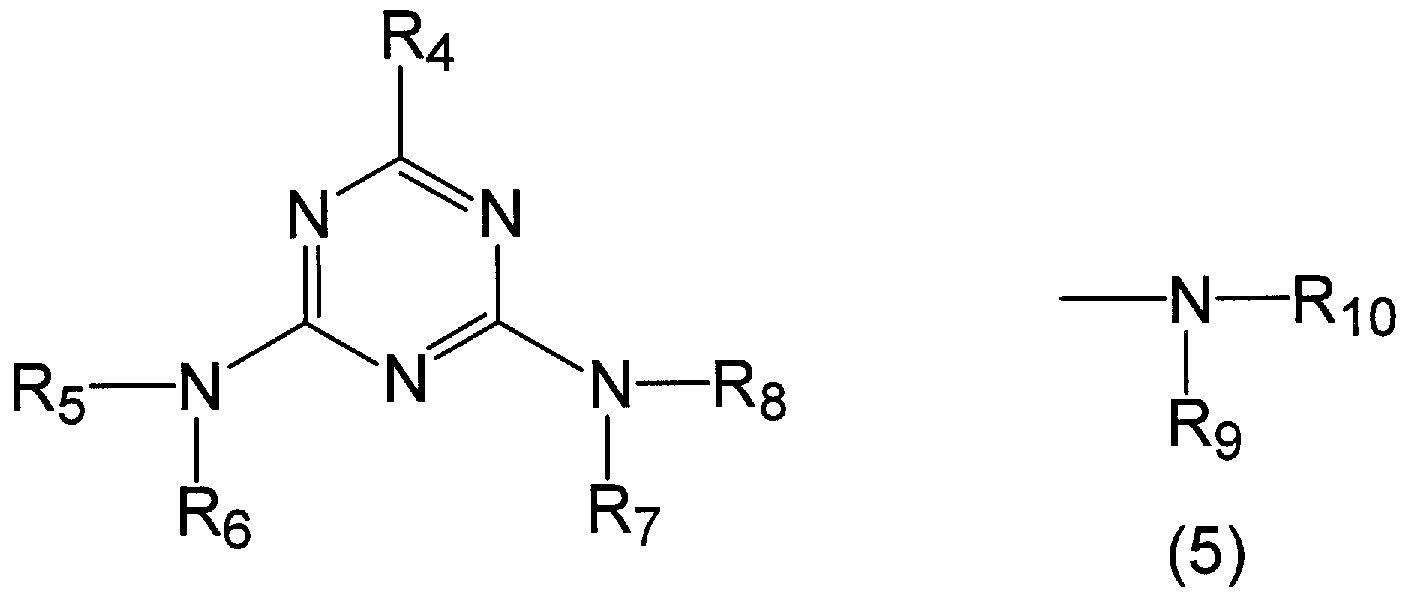
- R, R, R and R are each independently a hydroxymethyl group or an alcohol.
- R4 represents a phenyl group or a group represented by the formula (5), and in the formula (5), R
- R 9 and R each independently represent a hydroxymethyl group or an alkoxymethyl group
- composition for forming an antireflection film for lithography characterized in that it is a compound represented by
- the antireflection film-forming composition for lithography according to the first aspect, wherein the acid catalyst is an aromatic sulfonic acid compound,
- the step of applying the antireflection film-forming composition for lithography according to any one of the first to sixth aspects on a semiconductor substrate and baking to form an antireflection film Manufacturing a semiconductor device, comprising: forming a photoresist layer on an antireflection film; exposing a semiconductor substrate covered with the antireflection film and the photoresist layer; and developing the photoresist layer after exposure.
- the antireflection film-forming composition of the present invention has strong absorption against short-wavelength light, particularly KrF excimer laser (wavelength 248nm), ArF excimer laser (wavelength 193nm) or F2 excimer laser (wavelength 157nm). It is a composition for forming the anti-reflective film shown. The antireflection film thus obtained efficiently absorbs the reflected light from the substrate.
- the reflected light from the semiconductor substrate is effectively absorbed and a photoresist is obtained.
- An antireflection film that does not cause intermixing with the layer can be provided.
- a photoresist pattern having a good shape can be formed in a lithography process using a KrF excimer laser, an ArF excimer laser, or the like.
- the antireflection film-forming composition for lithography of the present invention comprises a sulfur-containing compound having a structure represented by the formula (1) as a partial structure, and a nitrogen atom substituted with a hydroxymethyl group or an alkoxymethyl group. It includes a reaction product obtained by reacting two or more nitrogen-containing compounds in the presence of an acid catalyst, and a solvent.
- the antireflection film-forming composition for lithography of the present invention can contain a polymer compound, a surfactant, a photoacid generator and the like in addition to the above compounds.
- the ratio of the solid content in the antireflection film-forming composition is not particularly limited as long as each component is uniformly dissolved in the solvent, but is, for example, 0.5 to 50% by mass, or: -30 mass%, or 3-25 mass%, or 5-: 15 mass%.
- the solid content is a value obtained by removing all components, solvent components, and the antireflection film-forming composition for lithography.
- the sulfur-containing compound can be used without particular limitation as long as it is a compound having the structure represented by the formula (1) as its partial structure.
- sulfur-containing compounds include thiourea and derivatives thereof, and cyclic compounds having the structure of the above formula (1) as a part of the ring structure, such as dithiouracil.
- R represents a hydrogen atom or an alkyl group having from 10 to 10 carbon atoms, and R represents water.
- R represents an alkyl group having 1 to 10 carbon atoms, a phenyl group, or naphthyl.
- the phenyl group, naphthyl group, and anthryl group are an alkyl group having 1 to 6 carbon atoms, a halogen atom, an alkoxy group having 1 to 6 carbon atoms, a cyan group, and a nitro group. Or substituted with a group selected from the group consisting of:
- an alkyl group examples thereof include a methinole group, an ethyl group, an isopropyl group, a cyclopentyl group, a normal hexynole group, a cyclooctyl group, and a 2_ethyl_1_hexyl group.
- the alkoxy group include a methoxy group, an ethoxy group, an isopropoxy group, a cyclohexenoreoxy group, and a normal pentyloxy group.
- Specific examples of the compound represented by the above formula (2) include thiorea, methylthiourea, 1,3_dimethylthiourea, 1,1_dimethylthiourea, ethylthiourea, acetylthiourea, benzoyl.
- Luciourea 1_Naphtylthiourea, 1_ (2-Chronophenyl) thiourea, 1,3-Dinormal butylthiourea, 1,3-Diphenylthiourea, 1—tert-Butyl-3-phenol Ruthiourea, 1,3-diphenyl 2-thiourea and the like.
- a cyclic compound having the structure of the formula (1) as a part of the ring structure can be used.
- examples of such a cyclic compound include dithiouracil, thiocyanouric acid, ethylenethiourea, 2-thiobarbituric acid, 2-thiouracil, and 5,5-dimethyl-2,4-dithiohydantoin.
- the nitrogen-containing compound for the reaction product in the antireflection film-forming composition for lithography of the present invention includes two or more nitrogen atoms substituted with a hydroxymethyl group or an alkoxymethyl group, such as two to two.
- a compound having six or four to six can be used.
- the alkoxymethyl group include a methoxymethylol group, an ethoxymethyl group, an isopropoxymethyl group, a normal butoxymethyl group, and a cyclohexyloxymethyl group.
- Such a nitrogen-containing compound repeats a compound having two or more N_H structures such as urea, melamine, benzoguanamine, and glycoluril, and a structure containing an amide group such as acrylamide and methacrylamide.
- a polymer compound having a unit structure can be reacted with formalin in boiling water to form hydroxymethyl on the nitrogen atom, thereby obtaining a compound having two or more hydroxymethyl groups.
- basic catalysts such as sodium hydroxide, potassium hydroxide and tetramethylammonium hydroxide can be used.
- alcohols such as methanol, ethanol, isopropanol, and normal hexanol are added to hydroxymethylated compounds. Can be obtained as a compound having an alkoxymethyl group.
- an acidic catalyst such as hydrochloric acid, sulfuric acid, and methanesulfonic acid can be used.
- R, R, R and R each represent a hydroxymethyl group or an alkoxymethyl group, and R represents a phenyl group or a group represented by the above formula (5).
- R 1 and R 2 each represent a hydroxymethyl group or an alkoxymethyl group.
- alkoxymethyl group include a methoxymethyl group, an ethoxymethyl group, an isopropoxymethyl group, a normal butoxymethyl group, and a cyclohexenoreoxymethyl group.
- nitrogen-containing compound for the reaction product in the antireflection film-forming composition for lithography of the present invention include hexamethoxymethyl melamine, hexatoxymethyl melamine, tetramethoxymethyl benzoguanamine, 1, 3 , 4, 6-tetrakis (butoxymethyl) glycoluril, 1, 3, 4, 6-tetrakis (hydroxymethinole) glycoluril, 1,3-bis (hydroxymethyl) urea, 1, 1, 3, 3 —Tetrakis (butoxymethyl) urea, 1,1,3,3-tetrakis (methoxymethyl) urea, 1,3-bis (hydroxymethyl) 4,5-dihydroxy-1-2-imidazolinone, and 1,3bis ( (Methoxymethyl) 1,4,5 dimethoxy-1-2-imidazolinone and the like.
- nitrogen-containing compounds examples include methoxymethyl type melamine compounds (trade names: Cymel 300, Saimenole 301, Saimenole 303, Cymel 350) manufactured by Nippon Cytec Industries Co., Ltd. (former Mitsui Cytec Co., Ltd.), butoxy Methyl type melamine compounds (trade names: Mycoat 506, Mycoat 508), compounds such as glycoluril compounds (trade names: Cymel 1170, Powder Link 1174), methyliurea resin (trade name UFR65), Petit Louis® urea resin ( Product name UFR300, U_VAN10S60, U—VAN10R, U—VAN11HV), Dainippon Ink & Chemicals Co., Ltd. urea Z formaldehyde resin (high condensation type, trade name Beckamine J
- Examples include commercially available compounds such as 300S, becamine P-955, and becamine N).
- the nitrogen-containing compound a compound obtained by reacting the compound represented by the formula (4) to increase the molecular weight can be used.
- a compound obtained by reacting the compound represented by the formula (4) to increase the molecular weight can be used.
- U.S. Pat. And high molecular weight compounds produced from triazine compounds (trade names such as Cymel 303 and Cymel 1123).
- the reaction product contained in the antireflection film-forming composition for lithography of the present invention comprises a sulfur-containing compound having a structure represented by the above formula (1) as a partial structure, and the hydroxymethyl group or alkoxy It can be obtained by reacting a nitrogen-containing compound having two or more nitrogen atoms substituted with a methyl group in the presence of an acid catalyst.
- organic acid compounds such as sulfonic acid compounds and carboxylic acid compounds, or inorganic acid compounds such as hydrochloric acid, sulfuric acid and nitric acid are used as the acid catalyst.
- Examples of the carboxylic acid compound include acetic acid, benzoic acid, salicylic acid, naphthalenecarboxylic acid, and butanoic acid.
- sulfonic acid compound examples include aliphatic sulfonic acid compounds such as methanesulfonic acid, trifluoromethanesulfonic acid, perfluorobutanesulfonic acid, and camphorsulfonic acid.
- sulfonic acid compounds include p-toluenesulfonic acid, sulfosalicylic acid, pyridinium ⁇ toluenesulfonic acid, 4-chlorobenzenesulfonic acid, 4-hydroxybenzenesulfonic acid, benzenedisulfonic acid, 1 naphthalenesulfonic acid, And pyridinium mu 1 aromatic sulfonic acid compounds such as naphthalenesulfonic acid
- the acid catalyst is, for example, 0.1 to 10 parts by mass or 0.1 part by mass with respect to 100 parts by mass of the sulfur-containing compound having a partial structure of the structure represented by the formula (1) used in the reaction. Used in a proportion of 5-5 parts by mass, or 1-3 parts by mass.
- a sulfur-containing compound having the structure represented by the formula (1) as a partial structure, and a nitrogen-containing compound having two or more nitrogen atoms substituted with a hydroxymethyl group or an alkoxymethyl group As the compounds, only one kind of compound can be used, or two or more kinds of compounds can be used in combination. Further, the ratio of the sulfur-containing compound having a partial structure of the structure represented by the formula (1) used in this reaction and the nitrogen-containing compound having two or more nitrogen atoms substituted with a hydroxymethyl group or an alkoxymethyl group As a molar ratio of sulfur-containing compound: nitrogen-containing compound is 4: 1 to 1: 4, or 3 ::! To 1: 3, or 3: 2 to 2: 3, or 4 : 3-3: 4, or 1: 1.
- This reaction is carried out in an organic solvent such as benzene, toluene, xylene, ethyl lactate, butyl lactate, propylene glycol monomethino ethenoreate, propylene glycol monomethino methenoate acetate, and N_methylpyrrolidone. Is done.
- the organic solvent is used in an amount of, for example, 1 to 100 times, or 5 to 50 times, or 10 to 30 times the total mass of the sulfur-containing compound, the nitrogen-containing compound and the acid catalyst used in the reaction. be able to.
- This reaction can be performed by appropriately selecting conditions from a reaction time of 0.:! To 100 hours and a reaction temperature of 20 ° C to 200 ° C.
- the reaction time is 0.5 to 10 hours, and the reaction temperature is 50 ° C to 150 ° C.
- reaction product is represented by formula (6) or formula (7):
- the molecular weight of the reaction product contained in the antireflection film-forming composition for lithography of the present invention is, for example, 500 to 100,000, or 1000 to 30000 as a weight average molecular weight (in terms of standard polystyrene), or 2000 ⁇ : 10,000.
- weight average molecular weight is smaller than the above value, the solubility of the formed antireflection film in the solvent used for the photoresist is increased, and as a result, intermixing with the photoresist may occur. If the weight average molecular weight is larger than the above value, uniform coating on the semiconductor substrate may be difficult.
- the isolated reaction product can be used. Also isolate the reaction product The reaction solution containing the reaction product can be used as it is in the antireflection film-forming composition for lithography of the present invention.
- the ratio of the reaction product to the solid content of the antireflection film-forming composition for lithography of the present invention is 50% by mass or more, for example, 60 to: 100% by mass, or 80 to 99.
- 99 mass 0/0, or 90 to 99.9 is the mass 0/0, or a 95 to 99.5 mass 0/0
- the antireflection film-forming composition for lithography of the present invention can also contain a polymer compound.
- polymer compound examples include addition polymerization polymers such as polyester, polystyrene, polyimide, acrylic polymer, methacrylic polymer, polybutyl ether, phenol novolak, naphthol novolak, polyester, polyamide, and polycarbonate. Rimmer can be used. From the viewpoint of light absorption performance, a polymer compound having an aromatic ring structure such as a benzene ring, naphthalene ring, anthracene ring, triazine ring, quinoline ring and quinoxaline ring is preferably used.
- Examples of such a polymer compound include benzyl acrylate, benzyl methacrylate, phenyl acrylate, naphthyl acrylate, anthryl methacrylate, anthryl methyl methacrylate, styrene, hydroxystyrene, and benzyl vinyl ether.
- addition polymerization polymers containing an addition polymerizable monomer such as N-phenylmaleimide as a structural unit and condensation polymerization polymers such as phenol novolak and naphthol novolak.
- polymer compound a polymer compound having no aromatic ring structure can be used.
- polymer compounds include, for example, alkyl acrylates, anorequinole methalelate, vinino elenotere, anorequinole vininoreatenore, attarilonitrinore, maleimide, N_alkylmaleimide, and maleic acid.
- An addition polymerization polymer containing only an addition polymerizable monomer having no aromatic ring structure such as an anhydride as its structural unit
- the polymer compound may be a homopolymer or a copolymer.
- Addition to the production of addition polymer A polymerizable monomer is used.
- Such addition polymerizable monomers include acrylic acid, methacrylic acid, acrylic ester compounds, methacrylic ester compounds, attalinoleamide compounds, methacrylamide compounds, bur compounds, styrene compounds, maleimide compounds, maleic acid. Anhydrides, acrylonitrile, etc. are mentioned.
- Examples of the acrylate compound include methyl acrylate, ethyl acrylate, normal hexyl acrylate, isopropyl acrylate, cyclohexyl acrylate, benzyl acrylate, phenyl acrylate, anthryl methyl acrylate.
- methacrylic acid ester compounds examples include methyl methacrylate, ethyl methacrylate, normal hexyl methacrylate, isopropyl methacrylate, cyclohexyl methacrylate, benzyl methacrylate, phenyl methacrylate.
- Anthrylmethyl Metatalylate 2-Oloetinoremetatalylate, 2,2,2_Trichloroethinoremetatalylate, 2-Bromoetinoremetatalylate, 4-Hydroxybutyl Metatalylate, 2-Methoxy Ethyl methacrylate, tetrahydrofurfuryl methacrylate, 2_methyl _2-adamantyl methacrylate, 5 methacryloyloxy _6—hydroxynorbornene 1_carboxyl 1-6-latathone, 3 _methacryloxypropyltri Ethoxysilane, glycidyl metatalylate, 2 —Phenylethyl metatalylate, hydroxyphenyl metatalylate, bromophenyl metatalylate, and the like.
- acrylamide compounds include acrylamide, N-methyl acrylamide, N-ethynole acrylamide, N-benzyl acrylamide, N phenyl acrylamide, N, N_dimethyl acrylamide, and N anthryl acrylamide.
- Methacrylamide compounds include methacrylamide, N-methylmethacrylamide, N-ethylmethacrylamide, N-benzylmethacrylamide, N-phenylmethacrylamide, ⁇ , ⁇ -dimethylmethacrylamide, and ⁇ ⁇ ⁇ - And anthryl methacrylamide.
- Examples of the bur compound include vinyl alcohol, 2-hydroxyethyl vinyl ether, methinorevinino reetenore, ethinolevinoleetenore, penzino levino reetenole, vinore acetic acid, butyltrimethoxysilane, 2_ Examples thereof include chloroethyl butyl ether, 2-methoxyethyl vinyl ether, urnaphthalene, and buranthracene.
- styrene compound examples include styrene, hydroxystyrene, chlorostyrene, bromostyrene, methoxystyrene, cyanostyrene, and acetyl styrene.
- maleimide compounds include maleimide, ⁇ -methylmaleimide, ⁇ -fuel maleimide, ⁇ -cyclohexylmaleimide, ⁇ -benzylmaleimide, and ⁇ -hydroxyethylmaleimide.
- the molecular weight of the polymer compound used in the antireflection film-forming composition for lithography of the present invention is, for example, 1000 to 1000000, or 3000 to 300000 as a weight average molecular weight (in terms of standard polystyrene). Also, for example, 5000-200000, or 10000-: 100000.
- composition for forming an antireflection film for lithography of the present invention contains a polymer compound
- the content thereof is, for example, 0.:! To 40% by mass in the solid content, or:! To 20 Or 3 to 19% by weight.
- the antireflection film-forming composition for lithography of the present invention can also contain a photoacid generator.
- the acidity of the antireflection film can be adjusted. This is used as one of the methods for matching the acidity of the antireflection film with the acidity of the upper photoresist. Further, by adjusting the acidity of the antireflection film, the pattern shape of the photoresist formed in the upper layer can be adjusted.
- Examples of the photoacid generator include onium salt compounds, sulfonimide compounds, and disulfonyl diazomethane compounds.
- onium salt compounds include diphenyl rhododonium hexafluorophosphate, Nylordon trifluoromethane sulfonate, Diphenylo nonafluo Mouth nore mano rebutans nore phonate, Di phene leo de nom perf Nore mano neno mano leo tan oleo tan octane sulfonate, dipheno Rhododonium camphorsulfonate, bis (4-tert-butylphenol) jordoncamphor sulfonate and bis (4_tert_butylphenyl) podonium trifluoromethanesulfonate, etc.
- Sulfonyl chloride compounds such as phenylsulfonium hexafluoroantimonate, triphenylsulfonium nonaf, noreo-normal-butane sulfonate, triphenylsulfonium camphorsulfonate, and triphenylsulfonium trifluoromethanesulfonate. Things And the like.
- Examples of the sulfonimide compound include N- (trifluoromethanesulfonyloxy) succinimide, N- (nonafluoro-normalbutanesulfonyloxy) succinimide, N (camphorsulfonyloxy) succinimide, and N (trifluoro). And romethanesulfonyloxy) naphthalimide.
- Examples of the disulfonyldiazomethane compound include bis (trifluoromethylsulfonyl) diazomethane, bis (cyclohexylsulfonyl) diazomethane, bis (phenylsulfonyl) diazomethane, and bis (p-toluenesulfoninole).
- Examples thereof include diazomethane, bis (2,4 dimethylbenzenesulfonyl) diazomethane, and methylsulfonyl-p-toluenesulfonyl diazomethane.
- the content thereof is, for example, 0.0:! To 5 mass% in the solid content, or :! ⁇ 3% by mass, or 0.5 ⁇ 2% by mass.
- a surfactant in addition to the above, a surfactant, a rheology adjusting agent, an adhesion aid, and the like can be added to the antireflection film-forming composition for lithography of the present invention, if necessary.
- Surfactants are effective in suppressing the generation of pinholes and strains.
- the rheology modifier improves the fluidity of the antireflective film-forming composition, and is effective in enhancing the fillability of the antireflective film-forming composition into the hole, particularly in the firing step.
- Adhesive assistant The auxiliary agent is effective for improving the adhesion between the semiconductor substrate or the photoresist and the antireflection film, and suppressing the peeling of the photoresist in the present image.
- surfactant examples include polyoxyethylene alkyl ethers such as polyoxyethylene lauryl ether, polyoxyethylene stearyl ether, polyoxyethylene cetyl ether, polyoxyethylene vinyl ether, and polyoxyethylene octyl phenol ether.
- Polyoxyethylene alkylaryl ethers such as polyoxyethylene nouryl phenol ether, polyoxyethylene polyoxypropylene block copolymers, sorbitan monolaurate, sorbitan monopalmitate, sorbitan monostearate, sorbitan monoole Sorbitan trioleate, sorbitan fatty acid esters such as sorbitan tristearate, polyoxyethylene sorbitan monolaurate, polyoxy Nonionic surfactants such as polyoxyethylene sorbitan fatty acid esters such as tylene sorbitan monopalmitate, polyoxyethylene sorbitan monostearate, polyoxyethylene sorbitan trioleate, polyoxyethylene sorbitan tristearate, and trade names F-top EF301, EF303, EF352 (manufactured by Gemco Co., Ltd.), trade names MegaFuck F171, F173, R—08, R—30 (manufactured by Dainippon Ink and Chemicals), Furadrad FC
- surfactants may be used alone or in combination of two or more.
- the content thereof is, in the solid content, 0.000:! To 5 mass% or 0.001 to 2 mass%, or 0 01 to 1% by mass.
- a solvent capable of dissolving the above-mentioned solid content can be used.
- solvents include, for example, ethylene glycol monomethino ethenore, ethylene glycol monomethino enoate, methyl cereal sorb acetate, cetyl solv acetate, diethylene glycol mono methino ethenore, diethylene glycol monomethenoate.
- a semiconductor substrate for example, a silicon wafer substrate, a silicon / silicon dioxide-coated substrate, a silicon nitride substrate, a glass substrate, an ITO substrate, etc.
- An antireflection film-forming composition is applied, and then fired to form an antireflection film.
- the conditions for firing are appropriately selected from firing temperatures of 80 ° C. to 250 ° C. and firing times of 0.3 to 60 minutes.
- the firing temperature is 150 ° C to 250 ° C
- the firing time is 0.5 to 3 minutes.
- ⁇ is in the range of 0.01 to 3.0 ⁇ ⁇ ⁇ , preferably in the order of 0.03 to 1.
- O zm Yes also ⁇ or 0.05 to 0.5 xm, and f or 0.05 to 0.5.
- a photoresist layer is formed on the antireflection film. Formation of the photoresist layer can be performed by a well-known method, that is, by applying and baking a photoresist composition solution on the antireflection film.
- the photoresist applied and formed on the antireflection film of the present invention is not particularly limited as long as it is sensitive to light used for exposure. Either negative photoresist or positive photoresist can be used.
- a positive photoresist composed of a novolak resin and 1,2_naphthoquinone diazide sulfonic acid ester, a chemically amplified type photocatalyst composed of a binder having a group that decomposes with an acid to increase the alkali dissolution rate and a photoacid generator.
- Low molecular weight compound that decomposes with dyst and acid to increase alkali dissolution rate of photoresist consisting of an acid, an alkali-soluble binder, and a photoacid generator, and a binder having a group that decomposes with an acid to increase the alkali dissolution rate and an acid to decompose to increase the alkali dissolution rate of the photoresist
- Low molecular weight compounds and photoacid generators such as chemically amplified photoresists.
- KrF excimer laser (wavelength 248 nm), ArF excimer laser (wavelength 193 nm), F2 excimer laser (wavelength 157 nm), or the like can be used.
- C Time 0.3 to: Can be performed under conditions selected as appropriate from 10 minutes.
- development is performed with a developer.
- a developer for example, when a positive photoresist is used, the exposed portion of the photoresist is removed, and a photoresist pattern is formed.
- Developers include aqueous solutions of alkali metal hydroxides such as potassium hydroxide and sodium hydroxide, aqueous solutions of quaternary ammonium hydroxides such as tetramethylammonium hydroxide, tetraethylammonium hydroxide and choline.
- alkaline aqueous solutions such as amine aqueous solutions such as ethanolamine, propylamine, and ethylenediamine.
- As the image liquid 2.38 mass% tetramethylammonium hydroxide aqueous solution which is widely used can be used.
- a surfactant or the like can be added to these developers.
- the conditions for the image are appropriately selected from a temperature of 5 to 50 ° C and a time of 10 to 300 seconds.
- the antireflection film is removed and the semiconductor substrate is processed.
- the antireflection film can be removed by using tetrafluoromethane, perfluorocyclobutane (CF), perfluoropropane (CF), trifluoromethane, carbon monoxide, argon, oxygen, nitrogen, sulfur hexafluoride, difluoromethane, trifluoromethane. This is performed using a gas such as nitrogen fluoride or chlorine trifluoride.
- An antireflection film is formed on a semiconductor substrate by the antireflection film forming composition for lithography of the present invention.
- a flat film or a gap fill material layer may be formed before the stop film is formed.
- the antireflection film formed from the composition for forming an antireflection film for lithography of the present invention includes a layer for preventing the interaction between the substrate and the photoresist, a material used for the photoresist, or a photoresist.
- a layer for preventing adverse effects on the substrate of the substance generated during exposure to the substrate, a layer for preventing diffusion of the substance generated from the substrate upon heating and baking into the upper photoresist, and a photo by the semiconductor substrate dielectric layer It can also be used as a barrier layer for reducing the resist layer's voiding effect.
- the via holes can be filled without any gaps. It can also be used as a possible embedding material. Further, it can be used as a flattening material for flattening the surface of an uneven semiconductor substrate.
- Hexamethoxymethylmelamine (10.0 g) and dithiolacinole (2.5 g) are dissolved in ethynole lactate (137.5 g), P-toluenesulfonic acid (0.3 g) is added, and the reaction product is reacted at 100 ° C for 3 hours. A solution containing was obtained.
- the weight average molecular weight was 2100 in standard polystyrene conversion.
- Hexamethoxymethylmelamine (10.0 g) and thiourea (2.5 g) are dissolved in 62.3 g of ethyl lactate, and then 0.3 g of p-toluenesulfonic acid is added and reacted at 80 ° C for 1 hour to contain the reaction product. A solution was obtained.
- the weight average molecular weight was 5100 in terms of standard polystyrene.
- Hexamethoxymethylmelamine 9.0g and thiourea 3.9g were dissolved in 63.6g of ethyl lactate, then 0.2g of p-toluenesulfonic acid was added and reacted at 80 ° C for 1 hour. A solution containing the product was obtained. When the GPC analysis of the obtained reaction product was conducted, the weight average molecular weight was 2000 in terms of standard polystyrene.
- Hexamethoxymethylmelamine 7.0g and thiourea 4.7g were dissolved in 57.7g of lactic acid ethynole, then 0.2g of p-toluenesulfonic acid was added and reacted at 80 ° C for 1 hour. A solution containing was obtained.
- the weight average molecular weight was 2700 in terms of standard polystyrene.
- Hexamethoxymethylmelamine (6.0 g) and thiourea (6.0 g) are dissolved in 59.4 g of lactic acid ethynole, p-toluenesulfonic acid (0.2 g) is added, and the reaction product is reacted at 80 ° C for 1 hour. A solution containing was obtained.
- the weight average molecular weight was 1800 in terms of standard polystyrene.
- Hexamethoxymethylmelamine 4 Og and ethylthiourea 1.7 g dissolved in 62.3 g ethyl lactate, P-toluenesulfonic acid 0. Ig is added and reacted at 120 ° C for 1 hour, including reaction products A solution was obtained. When the GPC analysis of the obtained reaction product was conducted, the weight average molecular weight was 46000 in terms of standard polystyrene.
- Hexamethoxymethylmelamine 8.5g and acetyl thiourea 2 Ig is dissolved in 52.9g of ethyl lactate, 0.2g of 5-sulfosalicylic acid is added and reacted at 80 ° C for 3 hours. A solution containing the product was obtained. When the obtained reaction product was subjected to GPC analysis, the weight average molecular weight was 920 in terms of standard polystyrene.
- Hexamethoxymethylmelamine 7.5g and acetyl thiourea 3.2g were dissolved in 53.4g of ethyl lactate, then 0.2g of 5-sulfosalicylic acid was added and reacted at 80 ° C for 3 hours. A solution containing the product was obtained. A GPC analysis of the obtained reaction product revealed that the weight average molecular weight was 870 in terms of standard polystyrene.
- Hexamethoxymethylmelamine 6.3g and acetyl thiourea 4.2g are dissolved in 52.3g of ethyl lactate, then 0.2g of 5_sulfosalicylic acid is added and reacted at 80 ° C for 3 hours. A solution containing the product was obtained.
- the weight average molecular weight was 800 in terms of standard polystyrene.
- Hexamethoxymethylmelamine 5.2g and acetyl thiourea 5.2g were dissolved in 51.8g of ethyl lactate, then 0.2g of 5_sulfosalicylic acid was added and reacted at 80 ° C for 3 hours. A solution containing the product was obtained. When GPC analysis of the obtained reaction product was performed, The weight average molecular weight was 660 in terms of styrene.
- Ethyl lactate 7.lg and acetyl thiourea 1.5g were added to 20.0g of the solution obtained in Synthesis Example 14, and reacted at 80 ° C for 3 hours to obtain a solution containing the reaction product.
- the weight average molecular weight was 15000 in standard polystyrene conversion.
- the weight average molecular weight was 13000 in standard polystyrene conversion.
- Hexamethoxymethylmelamine 7.5g and 1,3_dimethylthiourea 5.0g were dissolved in ethyl lactate 62.3g, then p-toluenesulfonic acid 0.3g was added and the mixture was heated at 80 ° C. Reaction was performed for 24 hours to obtain a solution containing the reaction product.
- the weight average molecular weight was 1900 in standard polystyrene conversion.
- Hexamethoxymethylmelamine (4.0 g) and 1,3-dimethylthiourea (4.0 g) were dissolved in ethyl acetate (39.8 g), 0.2 g of p-toluenesulfonic acid was added, and the mixture was stirred at 80 ° C. The reaction was carried out for a time to obtain a solution containing the reaction product.
- the weight average molecular weight was 3700 in terms of standard polystyrene.
- Hexamethoxymethylmelamine (7.5 g) and benzoinoretiourea (5.0 g) were dissolved in 62.3 g of lactate ethynole, and then added with p-toluenesulfonic acid (0.3 g) at 80 ° C. Reaction was performed for 3 hours to obtain a solution containing the reaction product.
- the weight average molecular weight was 670 in standard polystyrene conversion.
- an antireflection film (film thickness of 0.2 ⁇ m) was formed on the silicon wafer substrate from the solutions of Examples 1 to 23. Then, the dry etching rate of these antireflection films was measured under the conditions using a RIE system ES401 manufactured by Nippon Scientific Co., Ltd. and CF as a dry etching gas.
- a photoresist solution (product name: PAR710, manufactured by Sumitomo Chemical Co., Ltd.) was applied onto a silicon wafer substrate with a spinner and baked on a hot plate at 90 ° C for 1 minute to prepare a photoresist. A layer was formed. Then, using the RIE system ES401 manufactured by Nippon Scientific Co., Ltd., the dry etching rate of the photoresist PAR710 was measured under the condition that CF was used as the dry etching gas. A comparison was made between the dry etching rate of the film and the photoresist. The results are shown in Table 1. In Table 1, the selection ratio represents the dry etching rate of the antireflection film formed from each example when the dry etching rate of the photoresist PAR710 is 1.00.
- Example 1 8 2 .0 7 0 .3 0 2 .4 6
- Example 2 3 1. 9 2 0. 4 7 From Table 1, the antireflection film obtained from the antireflection film-forming composition of the present invention has an effective refractive index and attenuation coefficient for light having a wavelength of 248 nm. You can see that It can also be seen that the photoresist has a high dry etching rate.
Landscapes
- Engineering & Computer Science (AREA)
- Architecture (AREA)
- Structural Engineering (AREA)
- Physics & Mathematics (AREA)
- General Physics & Mathematics (AREA)
- Exposure Of Semiconductors, Excluding Electron Or Ion Beam Exposure (AREA)
- Materials For Photolithography (AREA)
- Macromolecular Compounds Obtained By Forming Nitrogen-Containing Linkages In General (AREA)
Description


Claims

Priority Applications (3)
| Application Number | Priority Date | Filing Date | Title |
|---|---|---|---|
| EP05788389.4A EP1811342B1 (en) | 2004-10-12 | 2005-09-27 | Use of a sulfur-atom-containing composition for forming of lithographic antireflection film |
| US11/664,989 US7795369B2 (en) | 2004-10-12 | 2005-09-27 | Sulfur atom-containing anti-reflective coating forming composition for lithography |
| JP2006540867A JP4687910B2 (ja) | 2004-10-12 | 2005-09-27 | 硫黄原子を含むリソグラフィー用反射防止膜形成組成物 |
Applications Claiming Priority (2)
| Application Number | Priority Date | Filing Date | Title |
|---|---|---|---|
| JP2004297640 | 2004-10-12 | ||
| JP2004-297640 | 2004-10-12 |
Publications (1)
| Publication Number | Publication Date |
|---|---|
| WO2006040921A1 true WO2006040921A1 (ja) | 2006-04-20 |
Family
ID=36148218
Family Applications (1)
| Application Number | Title | Priority Date | Filing Date |
|---|---|---|---|
| PCT/JP2005/017733 Ceased WO2006040921A1 (ja) | 2004-10-12 | 2005-09-27 | 硫黄原子を含むリソグラフィー用反射防止膜形成組成物 |
Country Status (7)
| Country | Link |
|---|---|
| US (1) | US7795369B2 (ja) |
| EP (1) | EP1811342B1 (ja) |
| JP (1) | JP4687910B2 (ja) |
| KR (1) | KR101216404B1 (ja) |
| CN (1) | CN100585496C (ja) |
| TW (1) | TWI361956B (ja) |
| WO (1) | WO2006040921A1 (ja) |
Cited By (6)
| Publication number | Priority date | Publication date | Assignee | Title |
|---|---|---|---|---|
| WO2009075265A1 (ja) * | 2007-12-13 | 2009-06-18 | Nissan Chemical Industries, Ltd. | レジスト下層膜形成組成物及びレジストパターンの形成方法 |
| JP2011527461A (ja) * | 2008-07-08 | 2011-10-27 | エイゼット・エレクトロニック・マテリアルズ・ユーエスエイ・コーポレイション | 反射防止コーティング組成物 |
| JP2012189988A (ja) * | 2010-12-31 | 2012-10-04 | Rohm & Haas Electronic Materials Llc | 上塗りフォトレジストと共に使用するためのコーティング組成物 |
| WO2015163195A1 (ja) * | 2014-04-25 | 2015-10-29 | 日産化学工業株式会社 | レジスト下層膜形成組成物及びそれを用いたレジストパターンの形成方法 |
| JP2016054149A (ja) * | 2007-11-14 | 2016-04-14 | コニカミノルタ株式会社 | 有機エレクトロルミネッセンス素子の製造方法 |
| US9475763B2 (en) | 2010-01-25 | 2016-10-25 | Rohm And Haas Electronic Materials Llc | Photoresist comprising nitrogen-containing compound |
Families Citing this family (4)
| Publication number | Priority date | Publication date | Assignee | Title |
|---|---|---|---|---|
| EP2472320A2 (en) | 2010-12-30 | 2012-07-04 | Rohm and Haas Electronic Materials LLC | Compositions comprising base-reactive component and processes for photolithography |
| US9170494B2 (en) | 2012-06-19 | 2015-10-27 | Az Electronic Materials (Luxembourg) S.A.R.L. | Antireflective compositions and methods of using same |
| WO2014103997A1 (ja) * | 2012-12-26 | 2014-07-03 | 富士フイルム株式会社 | 感光性樹脂組成物、硬化膜の製造方法、硬化膜、有機el表示装置および液晶表示装置 |
| KR102465032B1 (ko) * | 2022-06-24 | 2022-11-10 | 로움하이텍 주식회사 | 신규한 폴리이소시아누레이트, 이를 포함하는 반사 방지막 조성물 및 이를 채용하는 반사 방지막의 제조방법 |
Citations (3)
| Publication number | Priority date | Publication date | Assignee | Title |
|---|---|---|---|---|
| WO2002086624A1 (fr) * | 2001-04-10 | 2002-10-31 | Nissan Chemical Industries, Ltd. | Composition servant a former un film antireflet pour procede lithographique |
| WO2004034148A1 (ja) * | 2002-10-09 | 2004-04-22 | Nissan Chemical Industries, Ltd. | リソグラフィー用反射防止膜形成組成物 |
| WO2005088398A1 (ja) * | 2004-03-16 | 2005-09-22 | Nissan Chemical Industries, Ltd. | 硫黄原子を含有する反射防止膜 |
Family Cites Families (13)
| Publication number | Priority date | Publication date | Assignee | Title |
|---|---|---|---|---|
| US3317345A (en) | 1963-06-25 | 1967-05-02 | American Cyanamid Co | Rot-resistant finish for textile materials |
| US3300336A (en) * | 1963-09-09 | 1967-01-24 | Scient Chemicals Inc | Metal containing compositions, processes and products |
| US3310420A (en) * | 1965-10-05 | 1967-03-21 | Hooker Chemical Corp | Process for flameproofing cellulosic textile material |
| AU3488871A (en) | 1971-10-21 | 1973-05-03 | Commw Scient Ind Res Org | Process for stabilizing the shape of textile materials |
| JPS5882785A (ja) * | 1981-11-12 | 1983-05-18 | Kureha Chem Ind Co Ltd | 感圧記録紙用微小カプセル及びその製造方法 |
| JPS60220931A (ja) | 1984-03-06 | 1985-11-05 | Tokyo Ohka Kogyo Co Ltd | 感光性樹脂用下地材料 |
| JPS63309681A (ja) | 1987-06-10 | 1988-12-16 | 東海染工株式会社 | セルロ−ス系繊維含有構造体の塩素処理水に対する染色堅牢度向上法 |
| US5693691A (en) | 1995-08-21 | 1997-12-02 | Brewer Science, Inc. | Thermosetting anti-reflective coatings compositions |
| TW473653B (en) * | 1997-05-27 | 2002-01-21 | Clariant Japan Kk | Composition for anti-reflective film or photo absorption film and compound used therein |
| US5919599A (en) | 1997-09-30 | 1999-07-06 | Brewer Science, Inc. | Thermosetting anti-reflective coatings at deep ultraviolet |
| US6323310B1 (en) * | 2000-04-19 | 2001-11-27 | Brewer Science, Inc. | Anti-reflective coating compositions comprising polymerized aminoplasts |
| TW556047B (en) * | 2000-07-31 | 2003-10-01 | Shipley Co Llc | Coated substrate, method for forming photoresist relief image, and antireflective composition |
| JP2004123817A (ja) * | 2002-09-30 | 2004-04-22 | Nippon Shokubai Co Ltd | 光吸収性塗膜形成用組成物 |
-
2005
- 2005-09-27 WO PCT/JP2005/017733 patent/WO2006040921A1/ja not_active Ceased
- 2005-09-27 US US11/664,989 patent/US7795369B2/en not_active Expired - Lifetime
- 2005-09-27 CN CN200580034605A patent/CN100585496C/zh not_active Expired - Lifetime
- 2005-09-27 JP JP2006540867A patent/JP4687910B2/ja not_active Expired - Lifetime
- 2005-09-27 KR KR1020077010811A patent/KR101216404B1/ko not_active Expired - Lifetime
- 2005-09-27 EP EP05788389.4A patent/EP1811342B1/en not_active Expired - Lifetime
- 2005-10-06 TW TW094134977A patent/TWI361956B/zh not_active IP Right Cessation
Patent Citations (3)
| Publication number | Priority date | Publication date | Assignee | Title |
|---|---|---|---|---|
| WO2002086624A1 (fr) * | 2001-04-10 | 2002-10-31 | Nissan Chemical Industries, Ltd. | Composition servant a former un film antireflet pour procede lithographique |
| WO2004034148A1 (ja) * | 2002-10-09 | 2004-04-22 | Nissan Chemical Industries, Ltd. | リソグラフィー用反射防止膜形成組成物 |
| WO2005088398A1 (ja) * | 2004-03-16 | 2005-09-22 | Nissan Chemical Industries, Ltd. | 硫黄原子を含有する反射防止膜 |
Non-Patent Citations (1)
| Title |
|---|
| See also references of EP1811342A4 * |
Cited By (9)
| Publication number | Priority date | Publication date | Assignee | Title |
|---|---|---|---|---|
| JP2016054149A (ja) * | 2007-11-14 | 2016-04-14 | コニカミノルタ株式会社 | 有機エレクトロルミネッセンス素子の製造方法 |
| WO2009075265A1 (ja) * | 2007-12-13 | 2009-06-18 | Nissan Chemical Industries, Ltd. | レジスト下層膜形成組成物及びレジストパターンの形成方法 |
| JPWO2009075265A1 (ja) * | 2007-12-13 | 2011-04-28 | 日産化学工業株式会社 | レジスト下層膜形成組成物及びレジストパターンの形成方法 |
| US8361695B2 (en) | 2007-12-13 | 2013-01-29 | Nissan Chemical Industries, Ltd. | Resist underlayer film forming composition and method for forming resist pattern |
| JP2011527461A (ja) * | 2008-07-08 | 2011-10-27 | エイゼット・エレクトロニック・マテリアルズ・ユーエスエイ・コーポレイション | 反射防止コーティング組成物 |
| US9475763B2 (en) | 2010-01-25 | 2016-10-25 | Rohm And Haas Electronic Materials Llc | Photoresist comprising nitrogen-containing compound |
| JP2012189988A (ja) * | 2010-12-31 | 2012-10-04 | Rohm & Haas Electronic Materials Llc | 上塗りフォトレジストと共に使用するためのコーティング組成物 |
| WO2015163195A1 (ja) * | 2014-04-25 | 2015-10-29 | 日産化学工業株式会社 | レジスト下層膜形成組成物及びそれを用いたレジストパターンの形成方法 |
| US9910354B2 (en) | 2014-04-25 | 2018-03-06 | Nissan Chemical Industries, Ltd. | Resist underlayer film-forming composition and method for forming resist pattern using the same |
Also Published As
| Publication number | Publication date |
|---|---|
| CN100585496C (zh) | 2010-01-27 |
| JP4687910B2 (ja) | 2011-05-25 |
| JPWO2006040921A1 (ja) | 2008-05-15 |
| US20080118870A1 (en) | 2008-05-22 |
| TW200622497A (en) | 2006-07-01 |
| CN101040220A (zh) | 2007-09-19 |
| TWI361956B (en) | 2012-04-11 |
| KR101216404B1 (ko) | 2012-12-28 |
| EP1811342A4 (en) | 2010-06-09 |
| US7795369B2 (en) | 2010-09-14 |
| EP1811342A1 (en) | 2007-07-25 |
| EP1811342B1 (en) | 2013-07-10 |
| KR20070065433A (ko) | 2007-06-22 |
Similar Documents
| Publication | Publication Date | Title |
|---|---|---|
| TWI834605B (zh) | 對過氧化氫水溶液之保護膜形成組成物 | |
| JP4835854B2 (ja) | ハロゲン原子を有するナフタレン環を含むリソグラフィー用下層膜形成組成物 | |
| JP4247643B2 (ja) | 硫黄原子を含有する反射防止膜 | |
| JP3852593B2 (ja) | 反射防止膜形成組成物 | |
| JP4292910B2 (ja) | アセナフチレン誘導体、重合体および反射防止膜形成組成物 | |
| KR20040012537A (ko) | 아세나프틸렌 유도체, 중합체 및 반사 방지막 형성 조성물 | |
| JP5062420B2 (ja) | ポリシラン化合物を含むリソグラフィー用下層膜形成組成物 | |
| WO2011086757A1 (ja) | 感光性レジスト下層膜形成組成物及びレジストパターンの形成方法 | |
| US7687223B2 (en) | Underlayer coating forming composition for lithography containing cyclodextrin compound | |
| WO2010104074A1 (ja) | 側鎖にアセタール構造を有するポリマーを含むレジスト下層膜形成組成物及びレジストパターンの形成方法 | |
| JP4697464B2 (ja) | 含窒素芳香環構造を含むリソグラフィー用反射防止膜形成組成物 | |
| JP4687910B2 (ja) | 硫黄原子を含むリソグラフィー用反射防止膜形成組成物 | |
| JP4207119B2 (ja) | 多環脂環式構造ポリマーを含有する反射防止膜形成組成物 | |
| JP4207115B2 (ja) | リン系有機基含有高分子を含む反射防止膜形成組成物 | |
| WO2012147210A1 (ja) | レジスト下層膜形成用組成物及びパターン形成方法 | |
| JP4753018B2 (ja) | 付加重合性樹脂を含むリソグラフィー用反射防止膜形成組成物 | |
| JP4883286B2 (ja) | 傾斜構造を有するリソグラフィー用レジスト下層膜 | |
| JP2008152203A (ja) | 下層レジスト組成物、該組成物に有用な新規化合物、及び該組成物を用いたパターン形成方法 | |
| JP4952933B2 (ja) | 低感度感光性レジスト下層膜形成組成物 | |
| JPH0594018A (ja) | 感放射線性組成物 | |
| JP4214385B2 (ja) | シリコン原子を側鎖に有するポリマーを含む反射防止膜形成組成物 | |
| WO2025150548A1 (ja) | レジスト下層膜形成用組成物 | |
| WO2025173662A1 (ja) | レジスト下層膜形成用組成物及びレジスト下層膜 | |
| WO2025187721A1 (ja) | レジスト下層膜形成用組成物 | |
| TWI432906B (zh) | Method for forming composition and pattern of photoresist underlayer film formation |
Legal Events
| Date | Code | Title | Description |
|---|---|---|---|
| AK | Designated states |
Kind code of ref document: A1 Designated state(s): AE AG AL AM AT AU AZ BA BB BG BR BW BY BZ CA CH CN CO CR CU CZ DE DK DM DZ EC EE EG ES FI GB GD GE GH GM HR HU ID IL IN IS JP KE KG KM KP KR KZ LC LK LR LS LT LU LV LY MA MD MG MK MN MW MX MZ NA NG NI NO NZ OM PG PH PL PT RO RU SC SD SE SG SK SL SM SY TJ TM TN TR TT TZ UA UG US UZ VC VN YU ZA ZM ZW |
|
| AL | Designated countries for regional patents |
Kind code of ref document: A1 Designated state(s): BW GH GM KE LS MW MZ NA SD SL SZ TZ UG ZM ZW AM AZ BY KG KZ MD RU TJ TM AT BE BG CH CY CZ DE DK EE ES FI FR GB GR HU IE IS IT LT LU LV MC NL PL PT RO SE SI SK TR BF BJ CF CG CI CM GA GN GQ GW ML MR NE SN TD TG |
|
| 121 | Ep: the epo has been informed by wipo that ep was designated in this application | ||
| WWE | Wipo information: entry into national phase |
Ref document number: 2006540867 Country of ref document: JP |
|
| WWE | Wipo information: entry into national phase |
Ref document number: 200580034605.1 Country of ref document: CN Ref document number: 11664989 Country of ref document: US |
|
| NENP | Non-entry into the national phase |
Ref country code: DE |
|
| WWE | Wipo information: entry into national phase |
Ref document number: 2005788389 Country of ref document: EP |
|
| WWE | Wipo information: entry into national phase |
Ref document number: 1020077010811 Country of ref document: KR |
|
| WWP | Wipo information: published in national office |
Ref document number: 2005788389 Country of ref document: EP |
|
| WWP | Wipo information: published in national office |
Ref document number: 11664989 Country of ref document: US |