WO2006059531A1 - 光記録媒体用フィルタ、光記録媒体及びその製造方法、並びに光記録方法及び光再生方法 - Google Patents
光記録媒体用フィルタ、光記録媒体及びその製造方法、並びに光記録方法及び光再生方法 Download PDFInfo
- Publication number
- WO2006059531A1 WO2006059531A1 PCT/JP2005/021583 JP2005021583W WO2006059531A1 WO 2006059531 A1 WO2006059531 A1 WO 2006059531A1 JP 2005021583 W JP2005021583 W JP 2005021583W WO 2006059531 A1 WO2006059531 A1 WO 2006059531A1
- Authority
- WO
- WIPO (PCT)
- Prior art keywords
- optical recording
- recording medium
- light
- layer
- filter
- Prior art date
- Legal status (The legal status is an assumption and is not a legal conclusion. Google has not performed a legal analysis and makes no representation as to the accuracy of the status listed.)
- Ceased
Links
Classifications
-
- G—PHYSICS
- G03—PHOTOGRAPHY; CINEMATOGRAPHY; ANALOGOUS TECHNIQUES USING WAVES OTHER THAN OPTICAL WAVES; ELECTROGRAPHY; HOLOGRAPHY
- G03H—HOLOGRAPHIC PROCESSES OR APPARATUS
- G03H1/00—Holographic processes or apparatus using light, infrared or ultraviolet waves for obtaining holograms or for obtaining an image from them; Details peculiar thereto
- G03H1/02—Details of features involved during the holographic process; Replication of holograms without interference recording
- G03H1/0252—Laminate comprising a hologram layer
-
- G—PHYSICS
- G03—PHOTOGRAPHY; CINEMATOGRAPHY; ANALOGOUS TECHNIQUES USING WAVES OTHER THAN OPTICAL WAVES; ELECTROGRAPHY; HOLOGRAPHY
- G03H—HOLOGRAPHIC PROCESSES OR APPARATUS
- G03H1/00—Holographic processes or apparatus using light, infrared or ultraviolet waves for obtaining holograms or for obtaining an image from them; Details peculiar thereto
- G03H1/02—Details of features involved during the holographic process; Replication of holograms without interference recording
-
- G—PHYSICS
- G11—INFORMATION STORAGE
- G11B—INFORMATION STORAGE BASED ON RELATIVE MOVEMENT BETWEEN RECORD CARRIER AND TRANSDUCER
- G11B7/00—Recording or reproducing by optical means, e.g. recording using a thermal beam of optical radiation by modifying optical properties or the physical structure, reproducing using an optical beam at lower power by sensing optical properties; Record carriers therefor
- G11B7/24—Record carriers characterised by shape, structure or physical properties, or by the selection of the material
- G11B7/2403—Layers; Shape, structure or physical properties thereof
- G11B7/24035—Recording layers
- G11B7/24044—Recording layers for storing optical interference patterns, e.g. holograms; for storing data in three dimensions [3D], e.g. volume storage
-
- G—PHYSICS
- G03—PHOTOGRAPHY; CINEMATOGRAPHY; ANALOGOUS TECHNIQUES USING WAVES OTHER THAN OPTICAL WAVES; ELECTROGRAPHY; HOLOGRAPHY
- G03H—HOLOGRAPHIC PROCESSES OR APPARATUS
- G03H2250/00—Laminate comprising a hologram layer
- G03H2250/34—Colour layer
Definitions
- OPTICAL RECORDING MEDIUM FILTER OPTICAL RECORDING MEDIUM
- MANUFACTURING METHOD THEREOF OPTICAL RECORDING METHOD
- the present invention uses an optical recording medium filter suitably used as a wavelength selective reflection film in a hologram type optical recording medium capable of recording an unprecedented high-density image, and the optical recording medium filter.
- the present invention relates to an optical recording medium, a method of manufacturing the optical recording medium, and an optical recording method and an optical reproducing method using the optical recording medium.
- An optical recording medium is one of recording media capable of writing a large amount of information such as high-density image data.
- this optical recording medium for example, a rewritable optical recording medium such as a magneto-optical disk and a phase change type optical disk, and a write-once optical recording medium such as a CD-R, which are already in practical use, can be further used
- the demand for large capacity is increasing.
- all conventionally proposed optical recording media are two-dimensional recording, and there is a limit to increasing the recording capacity. Therefore, recently, a hologram type optical recording medium capable of recording information three-dimensionally has attracted attention.
- the hologram-type optical recording medium generally includes information light provided with a two-dimensional intensity distribution, and the information light and reference light having a substantially constant intensity superposed inside a photosensitive recording layer. Information is recorded by generating a distribution of optical characteristics inside the recording layer using the interference pattern formed by them. On the other hand, when reading (reproducing) the written information, the recording layer is irradiated with only the reference light in the same arrangement as during recording, and the reproduction has an intensity distribution corresponding to the optical characteristic distribution formed inside the recording layer. Light is emitted from the recording layer as light. In this hologram type optical recording medium, the optical characteristic distribution is three-dimensionally formed in the recording layer, so that the area where information is written by one information light and the information is written by other information light.
- a servo pit pattern 3 is provided on the surface of the lower substrate 1, and a reflective film 2 made of aluminum or the like is provided on the surface of the servo pit pattern.
- a recording layer 4 on the reflective film and an upper substrate 5 on the recording layer see Patent Document 2.
- the optical recording medium 20 having the configuration shown in FIG. 1 has a problem that the servo zone and the recording zone are separated in the plane, and the recording density is halved accordingly.
- Patent Document 3 circularly polarized light is used as information light and reference light, a cholesteric liquid crystal layer or dichroic mirror as a filter layer is provided between the recording layer and the reflective film, and the recording layer and the servo layer are made thick. Overlapping in the direction. This technique doubles the recording density.
- a single-layer cholesteric liquid crystal layer having a spiral structure having the same rotation direction as that of the circularly polarized light of information light is used as the filter layer, it is excellent in productivity and enables mass production of optical recording media at low cost.
- the filter effect at 0 ° incidence is good.
- this proposal when the incident angle changes, the selective reflection wavelength shifts.
- the incident light When the incident light is tilted by 10 ° or more, the information light and the reference light pass through the filter layer and reach the reflection film and are reflected. Arise. This means that it cannot be used for the incident light of the lens optical system in a normal optical recording medium of ⁇ 10 ° or more that is narrowed by the lens.
- the filter using the cholesteric liquid crystal layer is a method suitable for mass production because the production cost can be kept low.
- this filter with cholesteric liquid crystal layer force can reflect well when the writing light or reading light (350 to 600 nm) is only circularly polarized light, but it reflects when the recording system design changes to linearly polarized light or ordinary light. There is a problem that the rate drops to a minimum of 20%, and the amount of leaked light increases accordingly.
- Patent Document 1 JP 2002-123949 A
- Patent Document 2 JP-A-11 311936
- Patent Document 3 Japanese Patent Laid-Open No. 2004-265472
- the present invention prevents irregular reflection from the reflective film of the optical recording medium by information light and reference light, which does not cause a shift in the selective reflection wavelength even when the incident angle changes, and prevents the generation of noise.
- Filter for optical recording medium hologram type optical recording medium capable of high density recording using optical filter for optical recording medium, and optical recording medium capable of producing optical recording medium efficiently and at low cost It is an object of the present invention to provide a manufacturing method, and an optical recording method and an optical reproducing method using the optical recording medium.
- the filter for optical recording media of the present invention has a color material-containing layer containing a color material of at least one of a pigment and a dye.
- the color material is a red pigment
- the transmittance of 532 nm light in the red pigment is 33% or less
- the transmittance of 655 nm light is 66% or more
- Preferred is an aspect that is.
- the filter for optical recording media of the present invention has a color material-containing layer containing at least one of a pigment and a dye, so that, for example, the transmittance power for light of 532 nm is S33% or less, and 655 nm.
- the light transmittance is 66% or more, and it can absorb leakage light (532nm) that has passed through the filter and allow servo light (655nm) to pass through, thereby preventing noise.
- an aspect having a dielectric vapor deposition layer in which a plurality of dielectric thin films having different refractive indexes are laminated the dielectric vapor deposition layer has a low refractive index and a dielectric thin film having a low refractive index.
- An embodiment in which a plurality of layers of dielectric thin films having a refractive index are alternately laminated, an embodiment in which the dielectric vapor-deposited layer is laminated with 2 to 20 dielectric thin films, and an embodiment in which the dielectric vapor-deposited layer is provided on the colorant-containing layer are preferred.
- the color material-containing layer preferably the color material-containing layer
- the selective reflection wavelength does not shift even when the incident angle changes.
- the light transmittance at 655 nm at an incident angle of ⁇ 40 ° is 50% or more
- the light reflectivity at 532 nm is 30% or more, and the angle dependency of irradiation light reflection can be eliminated.
- the second wavelength light is 600 to 900 nm
- the light transmittance at 655 nm is 50% or more
- the light at 532 nm at an incident angle of ⁇ 40 ° is 30% or more
- an aspect used as a selective reflection film of an optical recording medium that records information using holography, and the optical recording medium uses the information light and the reference light as coaxial light beams.
- An aspect in which information is recorded by an interference pattern caused by interference between the information light and the reference light is preferable.
- the optical recording medium of the present invention includes an upper substrate, a lower substrate, a recording layer for recording information on the lower substrate using holography, and a space between the lower substrate and the recording layer. And a filter layer, and the filter layer has a color material-containing layer containing a color material of at least one of a pigment and a dye.
- the optical recording medium of the present invention with the above configuration, the information light and the reference light used during recording or reproduction without causing a deviation in the selective reflection wavelength even when the incident angle is changed, and the reproduction light are reflected on the reflection film. Therefore, diffused light due to irregular reflection on the reflecting surface can be prevented. Therefore, the noise generated by the diffused light is superimposed on the reproduced image and is not detected on the CMOS sensor or the CCD, but the reproduced image can be detected at least to the extent that error correction is possible.
- the noise component due to diffused light becomes a serious problem as the multiplicity of holograms increases.
- the embodiment in which the color material is a red pigment A mode in which the transmittance for light at 532 nm is 33% or less and the transmittance for light at 655 nm is 66% or more is preferable.
- the optical recording medium of the present invention since it has a colorant-containing layer containing at least one of a pigment and a dye, for example, the transmittance for 532 nm light is 33% or less, and 655 nm light Transmittance is 66% or more, and the leaked light (532nm) that has passed through the filter can be absorbed and the servo light (655nm) can be passed to prevent noise.
- the dielectric reflection layer is laminated on the color material-containing layer, preferably the color material-containing layer, so that the selective reflection wavelength does not shift even when the incident angle changes.
- the light transmittance at 655 nm is 50% or more
- the light reflectance at 532 nm is 30% or more, which eliminates the angle dependency of irradiation light reflection. it can.
- the filter layer transmits the light of the first wavelength and reflects the light of the second wavelength different from the light of the first wavelength, the first wavelength
- the light of 350 to 6 OOnm and the light of the second wavelength of 600 to 900 nm, the light transmittance at 655 nm for light within 40 ° within the filter layer is 50% or more
- An embodiment in which the light reflectance at 532 nm is 30% or more, an embodiment in which the substrate has a servo pit pattern, an embodiment in which a reflective film is provided on the surface of the servo pit pattern, and an embodiment in which the reflective film is a metal reflective film are preferred.
- the first gap layer for smoothing the substrate surface is provided between the filter layer and the reflective film.
- the first gap layer between the filter layer and the reflective film by providing the first gap layer between the filter layer and the reflective film, the reflective film can be protected and the size of the hologram generated in the recording layer can be adjusted. it can.
- an embodiment having a second gap layer between the recording layer and the filter layer is preferable.
- a point where information light and reproduction light are focused can be present. If this area is filled with a photopolymer, excessive consumption of monomer due to overexposure occurs, resulting in a decrease in multiple recording capability. Therefore, it is effective to provide a non-reactive and transparent second gap layer.
- a method of manufacturing an optical recording medium of the present invention is a method of manufacturing the optical recording medium of the present invention
- It includes at least a filter layer forming step of processing the optical recording medium filter of the present invention into an optical recording medium shape, and bonding the processed filter to the lower substrate to form a filter layer.
- an optical recording medium filter is cut into an optical recording medium shape, and the cut filter is bonded to the lower substrate to form a filter layer. Therefore, the optical recording medium can be mass-produced at a lower cost than the conventional method.
- the optical recording method of the present invention irradiates the optical recording medium of the present invention with information light and reference light as a coaxial beam, and records information by an interference pattern due to interference between the information light and the reference light. To record.
- the optical recording medium of the present invention is used to irradiate information light and reference light as a coaxial light beam, and information is obtained by an interference pattern due to interference between the information light and the reference light.
- unprecedented high-density recording can be realized.
- the interference pattern recorded on the recording layer by the optical recording method of the present invention can be read efficiently and accurately to reproduce high-density recorded information.
- FIG. 1 is a schematic cross-sectional view showing an example of the structure of a conventional optical recording medium.
- FIG. 2 is a graph showing a transmission spectrum of a red pigment.
- FIG. 3 is a graph showing reflection characteristics with respect to incident light from the front surface (0 °) of the filter for optical recording media.
- FIG. 4 is a graph showing the reflection characteristics with respect to incident light from a 40 ° tilt direction in the filter layer for optical recording media.
- FIG. 5 is a schematic sectional view showing an example of an optical recording medium according to the first embodiment of the present invention.
- FIG. 6 is a schematic sectional view showing an example of an optical recording medium according to the second embodiment of the present invention.
- FIG. 7 is an explanatory diagram showing an example of an optical system around an optical recording medium according to the present invention.
- FIG. 8 is a block diagram showing an example of the overall configuration of an optical recording / reproducing apparatus equipped with the optical recording medium of the present invention.
- Figure 9 shows the reflection characteristics by simulation when three layers of dielectric thin films are stacked. The left side shows the result of 0 ° incidence angle, and the right side shows the result of 40 ° incidence angle.
- FIG. 10 shows the reflection characteristics by simulation when five layers of dielectric thin films are stacked.
- the left side shows the result of the 0 ° incident angle, and the right side shows the result of the 40 ° incident angle.
- Fig. 11 shows the reflection characteristics by simulation when seven layers of dielectric thin films are laminated. The left side shows the result of 0 ° incidence angle, and the right side shows the result of 40 ° incidence angle.
- FIG. 12 shows the reflection characteristics by simulation when nine dielectric thin films are laminated.
- the left side shows the result of the 0 ° incident angle and the right side shows the result of the 40 ° incident angle.
- the filter for optical recording media of the present invention has at least a colorant-containing layer, and has a dielectric vapor deposition layer, a base material, and further other layers as necessary.
- the color material-containing layer contains a color material, and contains a binder resin, a solvent, and, if necessary, other components.
- Preferred examples of the coloring material include at least one of a pigment and a dye, and among these, from the viewpoint of absorbing light at 532 nm and transmitting servo light at 655 nm, a red dye and a red pigment are used. Particularly preferred are red pigments.
- the red dye can be appropriately selected according to the purpose from publicly known ones that are not particularly limited. If it is arranged, CI Acid Red 1, 8, 13, 14, 18, 26 , 27, 35, 37, 42, 52, 82, 87, 89, 92, 97, 106, 111, 114, 115, 134, 186, 249, 254, 28 9 etc .; CI Basic Red 2, 12 , 13, 14, 15, 18, 22, 23, 24, 27, 29, 35, 36, 38, 39, 46, 49, 51, 52, 54, 59, 68, 69, 70, 73, 78, 82 , 102, 104, 109, 112, etc .; CI Reactive Red 1, 14, 17, 25, 26, 32, 37, 44, 46, 55, 60, 66, 74, 79, 96, 97, etc. Reactive dyes, and the like. These may be used alone or in combination of two or more.
- the red pigment can be appropriately selected from known ones with no particular restrictions according to the purpose.
- a red pigment showing a transmission spectrum in which the transmittance for 532 nm light is 10% or less and the transmittance for 655 nm light is 90% or more is particularly preferable. Used.
- the content of the color material is preferably 0.05 to 90% by mass, more preferably 0.1 to 70% by mass, based on the total solid mass of the color material-containing layer. If the content is less than 0.05% by mass, the thickness of the color material-containing layer may be required to be 500 m or more, and 90% by mass When it exceeds%, the self-supporting property of the color material-containing layer is lost, and the film may collapse during the production process of the color material-containing layer.
- the Noinda rosin can be appropriately selected according to the purpose from known ones that are not particularly limited.
- polar binder groups epoxy group, COH, OH, NH, SOM, OSOM, POM, OPOM are included in the binder resin molecules mentioned above.
- M is a hydrogen atom, an alkali metal, or ammonia, and when there are multiple M's in one group, they may be different from each other.
- M is a hydrogen atom, an alkali metal, or ammonia, and when there are multiple M's in one group, they may be different from each other.
- the binder resins listed above are preferably cured by adding known isocyanate crosslinking agents.
- the content of the binder resin is 10 with respect to the total solid mass of the colorant-containing layer.
- Each of the above components is dissolved or dispersed in an appropriate solvent to prepare a coating solution, and this coating solution is applied onto a substrate described later by a desired coating method to form a color material-containing layer. It can be done.
- the solvent can be appropriately selected according to the purpose from known ones that are not particularly limited.
- water 3-methoxypropionic acid methyl ester, 3-methoxypropionic acid ethyl ester, 3-methoxypropion Acid propyl ester, 3-ethoxypropyl Alkoxypropionates such as lopionic acid methyl ester, 3-ethoxypropionic acid ethyl ester, and 3-ethoxypropionic acid propyl ester; alkoxy compounds such as 2-methoxypropinoacetate, 2 ethoxypropinolate acetate, and 3-methoxybutinolate acetate Esters of alcohols; Lactic acid esters such as methyl lactate and ethyl lactate; Ketones such as methyl ethyl ketone, cyclohexanone, and methylcyclohexanone; ⁇ Tyrolatatane, ⁇ -methylpyrrolidone, dimethyl sulfoxide, black mouth form,
- the coating method can be appropriately selected according to the purpose without any particular limitation.
- an inkjet method for example, an inkjet method, a spin coating method, a kneader coating method, a bar coating method, a blade coating method, a casting method, a dip method. , Curtain coating method, and the like.
- the thickness of the color material-containing layer is, for example, preferably 0.5 to 200 ⁇ m, more preferably 1.0 to LOO ⁇ m. If the thickness is less than 0.5 m, it may not be possible to add a sufficient amount of binder resin for wrapping the color material to form a film, and if it exceeds 200 / zm, the filter The thickness may become too large, and an excessively large optical system for irradiation light and servo light may be required.
- the dielectric vapor-deposited layer is formed on the colorant-containing layer, and is formed by laminating a plurality of dielectric thin films having different refractive indexes.
- a dielectric with a high refractive index is used.
- the present invention is not limited to two or more types, and more types may be used.
- the number of laminated layers is preferably 2 to 20 layers, more preferably 2 to 12 layers, and more preferably 4 to: 6 to 8 layers, more preferably the LO layer. If the number of laminated layers exceeds 20, the production efficiency may be reduced by multilayer deposition, and the object and effect of the present invention may not be achieved.
- the stacking order of the dielectric thin films can be appropriately selected according to the purpose without particular limitation. For example, when the refractive index of the adjacent film is high, a film having a lower refractive index is selected. Laminate first. Conversely, when the refractive index of the adjacent layer is low, a film having a higher refractive index is first laminated. The boundary between high and low refractive index is 1.8. In addition, It is not absolute whether the refractive index is high or low. Among high-refractive-index materials, there may be a material with a relatively high refractive index and a material with a relatively low refractive index. I don't know.
- Examples of the material for the high refractive index dielectric thin film include Sb 2 O, Sb 2 S, Bi 2 O, and Ce.
- HfO, SiO, Ta O, TiO, Y 2 O, ZnSe, ZnS, ZrO are preferred.
- SiO, TaO, TiO, Y2O, ZnSe, ZnS and ZrO are particularly preferred.
- Examples of the material for the low refractive index dielectric thin film include Al 2 O, BiF, CaF, and LaF.
- 2 3 3 2 2 2 2 3 is preferred, and Al O, CaF, MgF, MgO, SiO, and Si O are particularly preferred.
- the atomic ratio can be appropriately selected depending on the purpose, and the atomic ratio can be adjusted by changing the atmospheric gas concentration during film formation. it can.
- the method for forming the dielectric thin film is not particularly limited, and can be appropriately selected according to the purpose.
- the vacuum deposition method, the sputtering method, the ion plating method, the ion beam method, the ion beam method examples include the physical vapor deposition (PVD) method such as the assist method and the laser ablation method, the chemical vapor deposition (CVD) method such as the thermal CVD method, the photo CVD method, and the plasma CVD method.
- PVD physical vapor deposition
- CVD chemical vapor deposition
- the sputtering method, in which the physical vapor deposition (PVD) method is preferable is particularly preferable.
- a DC sputtering method having a high film formation rate is preferable.
- the DC sputtering method it is preferable to use a material having high conductivity.
- a method of forming a multilayer film by sputtering for example, (1) one chamber method in which a single chamber forms a film alternately or sequentially from a plurality of targets, and (2) a plurality of chambers continuously.
- the multi-chamber method is particularly preferable from the viewpoint of preventing productivity and material contamination.
- the thickness of the dielectric thin film is preferably on the order of the optical wavelength, with a thickness of ⁇ 6 to 6 mm, preferably 8 to 3 4 mm, and preferably 6 to 3 8 mm.
- the light propagating in the dielectric deposition layer is partially reflected by each dielectric thin film, and the reflected light interferes with the thickness of the dielectric thin film. Only light having a wavelength determined by the product of the refractive index of the film with respect to the light is selectively transmitted.
- the central transmission wavelength of the dielectric deposition layer has an angle dependency with respect to the incident light, and the transmission wavelength can be changed by changing the incident light.
- the number of stacked layers of the dielectric vapor deposition layers is 20 or less, several% to several tens of% selective reflection wavelength light leaks through the filter and transmits, but the leaked light is directly under the dielectric vapor deposition layers. It is absorbed by the color material-containing layer charged in. Since the color material-containing layer contains a red pigment or a red dye, the light of 350 to 600 nm is absorbed. The light of 600 to 900 nm used as servo light is transmitted.
- the function of the optical recording medium filter having the color material-containing layer and the dielectric vapor deposition layer is to transmit light having a first wavelength and reflect light having a second wavelength different from the light having the first wavelength. More specifically, it is preferable that the light of the first wavelength is 350 to 600 nm and the light of the second wavelength is 600 to 900 nm.
- an optical recording medium having a structure in which a recording layer, an dielectric vapor deposition layer, a colorant-containing layer, and a servo bit pattern are laminated in this order is preferable.
- the optical recording medium filter has an optical transmittance at 655 nm of 50% or more (preferably 80% or more) at an incident angle of ⁇ 40 °, and an optical reflectance at 532 nm of 30. % Or more (preferably 40% or more).
- an optical recording medium filter having a colorant-containing layer and a dielectric vapor deposition layer has reflection characteristics shown in FIG. 3 with respect to normal incident light from the front surface (0 °).
- the incident light comes from an oblique direction, it gradually shifts to the short wavelength side, and shows a reflection characteristic as shown in Fig. 4 when inclined by 40 °.
- the method for producing the filter for optical recording media can be appropriately selected according to the purpose without any particular restrictions. For example, (1) a color material-containing layer is formed on a substrate described later. (2) a mixture of the binder resin and the color material as the first gap layer 8 in FIGS. 5 and 6; And the like.
- the thickness of the optical recording medium filter (total thickness of the colorant-containing layer and the dielectric deposition layer excluding the base material) is preferably, for example, 0.5 to 200 ⁇ m. m is more preferable.
- the optical recording medium filter can be appropriately selected depending on the purpose without any particular restriction, and is processed into a disk shape (for example, punching) on the base material to be described later. It is preferably arranged on the lower substrate. Further, when used for a filter layer of an optical recording medium, the filter layer can be provided directly on the lower substrate without using a base material.
- the shape, structure, size, etc. of the substrate can be appropriately selected according to the purpose without any particular restrictions.
- Examples of the shape include a flat plate shape, a sheet shape, etc.
- any of inorganic materials and organic materials that are not particularly limited can be suitably used.
- Examples of the inorganic material include glass, quartz, and silicon.
- organic material examples include acetate-based resins such as triacetyl cellulose, polyester-based resins, polyethersulfone-based resins, polysulfone-based resins, polycarbonate-based resins, polyamide-based resins, and polyimide-based resins.
- examples thereof include fats, polysalt-vinylidene-based resins, and polyacrylic resins. These may be used alone or in combination of two or more.
- the base material may be appropriately synthesized! Or a commercially available product may be used.
- the thickness of the substrate is not particularly limited and can be appropriately selected according to the purpose.
- the thickness force of the substrate is less than 10 m, the adhesion may be lowered due to the stagnation of the substrate.
- the distance exceeds 500 m the focal positions of the information beam and the reference beam must be greatly shifted, and the optical system size increases.
- the optical recording medium filter of the present invention can be used in various fields, and can be suitably used for forming or manufacturing a holographic optical recording medium. It can be particularly suitably used for an optical recording medium, a production method thereof, an optical recording method, and an optical reproduction method.
- the optical recording medium of the present invention comprises an upper substrate, a lower substrate, a recording layer on the lower substrate, and a filter layer between the lower substrate and the recording layer. It includes a film, a first gap layer, a second gap layer, and other layers as necessary.
- the optical recording medium filter of the present invention is used.
- the shape, structure, size, etc. of the substrate can be appropriately selected according to the purpose without any particular restrictions.
- Examples of the shape include a disk shape, a card shape, and the like. It is necessary to select materials that can ensure the mechanical strength of the media.
- it when light used for recording and reproduction is incident through the substrate, it must be sufficiently transparent in the wavelength region of the light used.
- the substrate material glass, ceramics, resin, etc. are usually used, but resin is particularly preferred from the viewpoint of formability and cost.
- the resin examples include polycarbonate resin, acrylic resin, epoxy resin, polystyrene resin, acrylonitrile styrene copolymer, polyethylene resin, polypropylene resin, silicone resin, fluorine resin, ABS resin. Fat, urethane slag, etc. are mentioned.
- polycarbonate resin and acrylic resin are particularly preferable from the viewpoints of moldability, optical properties, and cost.
- the substrate may be appropriately synthesized or a commercially available product may be used.
- the substrate is provided with address servo areas as a plurality of positioning regions extending linearly in the radial direction at predetermined angular intervals, and a sectoral section between adjacent address servo areas becomes a data area.
- address servo area information for performing focus servo and tracking servo by the sampled servo system and address information are recorded in advance by embossed pits (servo pits) (pre-format).
- servo pits pre-format
- the focus servo can be performed using the reflective surface of the reflective film.
- a wobble pit can be used. If the optical recording medium has a card shape, the servo pit pattern may be omitted.
- the thickness of the substrate is not particularly limited and can be appropriately selected according to the purpose, and is preferably 0.1 to 5 mm, more preferably 0.3 to 2 mm. If the thickness of the substrate is less than 0.1 mm, the distortion of the shape during storage of the disc may not be suppressed. If the thickness exceeds 5 mm, the overall weight of the disc increases and an excessive load is applied to the drive motor. There are times.
- the recording layer can record information using holography, and a material whose optical characteristics such as an extinction coefficient and a refractive index change according to the intensity of the recording layer when irradiated with an electromagnetic wave having a predetermined wavelength is used. .
- the material of the recording layer is not particularly limited and can be appropriately selected according to the purpose.
- a photopolymer that undergoes polymerization reaction upon irradiation with light and becomes a polymer (2) photopolymer Photorefractive materials exhibiting a fractive effect (refractive index modulation is caused by light charge distribution due to light irradiation), (3) photochromic materials in which molecular isomerism is induced by light irradiation and refractive index is modulated, (4 ) Inorganic materials such as lithium niobate and barium titanate, and (5) chalcogen materials.
- the photopolymer of (1) is not particularly limited and can be appropriately selected depending on the purpose. For example, it contains a monomer and a photoinitiator, and further, if necessary, a sensitizer. And other components such as oligomers.
- Examples of the photopolymer include "Photopolymer Handbook” (Industry Research Committee, 1 989), “Photopolymer Technology” (Nikkan Kogyo Shimbun, 1989), SPIE Proceedings Vol. 3010 p354—372 (1997), and SPIE Proceedings Vol. 3291 p89—103 (199). Can be used. Also, U.S. Patent Nos. 5,759,721, 4,942,112, 4,959,284, 6,221,536, WO97Z44714, 97Z13183, 99Z26112 Pamphlet, pamphlet 97Z13183, pamphlet No. 2880342, pamphlet 2873126, pamphlet 2849021, pamphlet 3057082, pamphlet 3161230, JP 2001-316416, JP 2000- Photopolymers described in Japanese Patent No. 275859, etc. can be used.
- Examples of the method of changing the optical characteristics by irradiating the photopolymer with recording light include a method using diffusion of a low molecular component.
- a component that diffuses in the opposite direction to the polymerization component may be added, or a compound having an acid cleavage structure may be added separately in addition to the polymer.
- a structure capable of holding a liquid in the recording layer may be required.
- the compound having the acid cleavage structure is added, the volume change may be suppressed by compensating for the expansion caused by the cleavage and the shrinkage caused by the polymerization of the monomer.
- the monomer can be appropriately selected according to the purpose without any particular limitation.
- a radical polymerization type monomer having an unsaturated bond such as an acryl group or a methacryl group, an epoxy ring oxetane.
- examples thereof include a cationic polymerization type monomer having an ether structure such as a ring.
- These monomers may be monofunctional or polyfunctional.
- you may utilize a photocrosslinking reaction.
- radical polymerization type monomer examples include, but are not limited to, allyloyl morpholine, phenoxy shetyl acrylate, isobornyl acrylate, 2-hydroxypropyl acrylate, 2-ethyl hexyl acrylate, 1,6 hexanediol Diatalylate, Tripropylene glycol diatalylate, Neopentyl glycol PO-modified diatalylate, 1,9-nonanediol diatalylate, Hydroxypivalate neopentylglycol diatalylate, EO-modified bisphenol A diatalylate, Polyethylene glycol diatalylate ,pen Taerythritol Triatalylate, Pentaerythritol Tetratalylate, Pentaerythritol Hexaatalylate, EO Modified Glycerol Tritalylate, Trimethylolpropane Triata
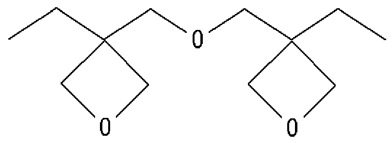
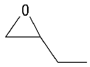
- Examples of the cationic polymerization-type monomer include bisphenol A epoxy resin, phenol novolac epoxy resin, glycerol triglycidyl ether, 1,6 hexane glycidyl ether, butyltrimethoxysilane, and 4-butylphenol trimethoxysilane. , ⁇ -methacryloxypropyltriethoxysilane, compounds represented by the following structural formulas ( ⁇ ) to ( ⁇ ), and the like.
- These monomers may be used alone or in combination of two or more.
- Examples of the photoinitiator include materials that cause radical polymerization, cationic polymerization, crosslinking reaction, and the like by light irradiation as long as they are sensitive to recording light.
- photoinitiator examples include 2,2 ′ bis (o black-mouthed) -4,4 ′, 5,5′tetraphenyl-1,1, -biimidazole, 2,4,6 tris (Trichloromethyl) -1,3,5-triazine, 2,4 Bis (trichloromethyl) 6- (p-methoxyphenol) 1,3,5-triazine, diphenyl tetrafluor Fluoroborate, Diphenyl-Hexafluorophosphate, 4, 4'-tert-Butyl Diphenyl-Fluorodium Tetra Fluoroborate, 4-Jetylaminophenol Benzenediazo-Mumoxafluorophosphate, Benzoin 2-hydroxy-1-2-methyl 1-phenolpropane-2-one Benzophenone, thixanthone, 2,4,6-trimethylbenzoyldiphenylsylphosphine oxide, triphenylbutyl borate tetraethylam
- the photopolymer can be obtained by stirring and mixing the monomer, the photoinitiator, and, if necessary, other components and reacting them. If the obtained photopolymer has a sufficiently low viscosity, a recording layer can be formed by casting. On the other hand, in the case of a high-viscosity photopolymer that cannot be cast, a photopolymer is placed on the lower substrate using a dispenser, pressed onto the photopolymer so that the upper substrate is covered, and spread over the entire surface to form a recording layer. Can be formed.
- the photorefractive material of (2) can be appropriately selected according to the purpose without particular limitation as long as it exhibits a photorefractive effect.
- a charge generating material and a charge transporting material And other components as necessary.
- the charge generating material can be appropriately selected depending on the purpose without any particular limitation.
- Phthalocyanine dyes such as metal phthalocyanine, metal-free phthalocyanine, or derivatives thereof z pigments; naphthalocyanine dyes z pigments; azo dyes such as monoazo, disazo and trisazo Z pigments; perylene dyes Z pigments; indigo Dye Z pigments; Quinacridone dyes Z pigments; Polycyclic quinone dyes such as anthraquinone and anthanthrone Z pigments; cyanine dyes Z pigments; electron accepting and electron donating substances such as TTF-TCNQ Charge-transfer complex; azurenium salt; fullerene represented by C and C
- methanofullerene which is a derivative thereof. These may be used alone or in combination of two or more.
- the charge transport material is a material that transports holes or electrons, and may be a low molecular compound or a high molecular compound.
- the charge transport material is not particularly limited and can be appropriately selected according to the purpose.
- Nitrogen-containing cyclic compounds such as, or derivatives thereof; hydrazone compounds; triphenylamines; triphenylmethanes; butadienes; stilbenes; quinone compounds such as anthraquinone diphenoquinone, or derivatives thereof; C and C Fullerenes and derivatives thereof;
- ⁇ - conjugated polymers or oligomers such as polyacetylene, polypyrrole, polythiophene, and polyarine; ⁇ - conjugated polymers or oligomers such as polysilane and polygerman; polycyclic aromatic compounds such as anthracene, pyrene, phenanthrene, and coronene, etc. Is mentioned. These may be used alone or in combination of two or more.
- a coating film is formed using a coating solution obtained by dissolving or dispersing the photorefractive material in a solvent, and this coating film is formed.
- the recording layer can be formed by removing the solvent from the recording medium.
- the recording layer can be formed by forming a coating film using the photorefractive material that has been heated and fluidized, and rapidly cooling the coating film.
- the photochromic material (3) is not particularly limited as long as it is a material that causes a photochromic reaction, and can be appropriately selected according to the purpose.
- an azobenzene compound, a stilbene compound, an indigo compound , Thioindigo compounds, spiropyran compounds, spiro Examples include xazazine compounds, fluorinated compounds, anthracene compounds, hydrazone compounds, cinnamic acid compounds, and the like.
- azobenzene derivatives and stilbene derivatives that undergo structural changes due to cis-trans isomerism upon irradiation with light
- spiropyran derivatives and spiroxazine derivatives that undergo structural changes between ring opening and ring closure upon irradiation with light.
- the chalcogen material (5) includes, for example, a chalcogenide glass containing a chalcogen element, and metal particles having a metal force that are dispersed in the chalcogenide glass and can diffuse into the chalcogenide glass by light irradiation. Materials, etc. included.
- the chalcogenide glass is not particularly limited as long as it has a non-acidic amorphous material strength containing a chalcogen element such as S, Te or Se, and can dope metal particles.
- Examples of the amorphous material containing the chalcogen element include Ge—S glass, As—S glass, As—Se glass, As—Se—Ce glass, and the like. S glass is preferred.
- Ge-S glass is used as the chalcogenide glass, the composition ratio of Ge and S constituting the glass can be arbitrarily changed according to the wavelength of light to be irradiated.
- Id glass is preferred.
- the metal particles are not particularly limited as long as they have the property of being light-doped into chalcogenide glass by light irradiation, and can be appropriately selected according to the purpose.
- Ag, Au, or Cu has a characteristic that it is more likely to cause light doping, and Ag is particularly preferable because it significantly causes light doping.
- the content of the metal particles dispersed in the chalcogenide glass is preferably 0.1 to 2% by volume based on the total volume of the recording layer, and more preferably 0.1 to 1.0% by volume. If the content of the metal particles is less than 0.1% by volume, the change in transmittance due to light doping may be insufficient, and the recording accuracy may decrease. If the content exceeds 2% by volume, the recording material Therefore, it may be difficult to sufficiently generate optical dope.
- the recording layer can be formed according to a known method depending on the material.
- a vapor deposition method, a wet film formation method, an MBE (molecular beam epitaxy) method, a cluster ion beam method It can be suitably formed by a molecular lamination method, LB method, printing method, transfer method, or the like.
- the vapor deposition method and the wet film forming method are preferable.
- the vapor deposition method can be appropriately selected from known methods according to the purpose without any particular limitation, and examples thereof include vacuum vapor deposition, resistance heating vapor deposition, chemical vapor deposition, and physical vapor deposition. Can be mentioned.
- Examples of the chemical vapor deposition method include a plasma CVD method, a laser C VD method, a thermal CVD method, and a gas source CVD method.
- Formation of the recording layer by the wet film-forming method is preferably performed by using (coating and drying) a solution (coating liquid) in which the recording layer material is dissolved or dispersed in a solvent.
- a solution coating liquid
- a known medium force can be appropriately selected according to the purpose without any particular limitation. For example, an ink jet method, a spin coat method, a kneader coat method, a bar coat method, a blade coat method, a cast Law, dipping method, curtain coating method, etc.
- the thickness of the recording layer in particular limitation put out be appropriately selected depending on the Nag purposes, 1 ⁇ : LOOO / zm force preferably, 100 to 700 111 Ca ⁇ Yori preferably 1 ⁇ 0
- the thickness of the recording layer is within the preferable numerical range, a sufficient SZN ratio can be obtained even when shift multiplexing of 10 to 300 is performed, and when the thickness is within the more preferable numerical range, this is remarkable. It is advantageous in some respects.
- the reflective film is formed on the surface of the servo pit pattern of the substrate.
- the material of the reflective film it is preferable to use a material having a high reflectance with respect to the recording light and the reference light.
- the wavelength of light to be used is 400 to 780 nm, for example, Al, A1 alloy, Ag, Ag alloy, etc. are preferably used.
- the wavelength of light to be used is 650 nm or more, it is preferable to use Al, A1 alloy, Ag, Ag alloy, Au, Cu alloy, TiN, or the like.
- an optical recording medium that reflects light and can be added or deleted, such as a DVD (digital video disc), is used. Does not affect the hologram, such as directory information, such as whether or not there is an error and how the replacement process was performed It is also possible to add and rewrite to.
- the formation of the reflective film is not particularly limited and can be appropriately selected according to the purpose.
- Various vapor deposition methods such as vacuum deposition, sputtering, plasma CVD, photo-CVD, ion A plating method, an electron beam evaporation method, or the like is used.
- the sputtering method is excellent in terms of mass productivity and film quality.
- the thickness of the reflective film is preferably 50 nm or more, more preferably 1 OOnm or more so that sufficient reflectivity can be achieved.
- the first gap layer is provided between the filter layer and the reflective film as needed, and is formed for the purpose of smoothing the lower substrate surface. It is also effective for adjusting the size of the hologram generated in the recording layer. That is, since it is necessary to form the recording reference light and the information light interference area in a certain size in the recording layer, it is effective to provide a gap between the recording layer and the servo pit pattern.
- the first gap layer can be formed, for example, by applying a material such as an ultraviolet curable resin with an upper force of the servo pit pattern by spin coating or the like and curing it.
- a material such as an ultraviolet curable resin with an upper force of the servo pit pattern by spin coating or the like and curing it.
- the transparent substrate also functions as the first gap layer.
- the thickness of the first gap layer can be appropriately selected according to the purpose without particular limitation, and is preferably 1 to 200 m.
- the second gap layer is provided between the recording layer and the filter layer as necessary.
- the material of the second gap layer is not particularly limited and can be appropriately selected according to the purpose.
- triacetyl cellulose TAC
- PC polycarbonate
- PET polyethylene terephthalate
- PS polystyrene
- PSF polysulfone
- PVA polybulal alcohol
- PMMA polymethyl methacrylate
- transparent resin film or JSR brand name ARTON film or Japan
- a norbornene-based resin film such as Zeon's trade name Zeonor.
- TAC, PC, trade name ARTON, and trade name Zeonor are preferred because they are highly isotropic. Is particularly preferred.
- the thickness of the second gap layer can be appropriately selected according to the purpose without particular limitation, and is preferably 1 to 200 m.
- FIG. 5 is a schematic cross-sectional view showing the configuration of the optical recording medium in the first embodiment of the present invention.
- a servo pit pattern 3 is formed on a polycarbonate resin substrate or glass substrate 1, and the servo pit pattern 3 is coated with aluminum, gold, platinum, or the like.
- a reflective film 2 is provided.
- the force that the servo pit pattern 3 is formed on the entire surface of the lower substrate 1 may be formed periodically as shown in FIG.
- the height of the servo pit pattern 3 is normally 1750 A (175 nm), which is sufficiently smaller than the thickness of the substrate and other layers.
- the first gap layer 8 is formed by applying a material such as ultraviolet curable resin on the reflective film 2 of the lower substrate 1 by spin coating or the like.
- the first gap layer 8 is effective for protecting the reflective film 2 and adjusting the size of the hologram generated in the recording layer 4. That is, since it is necessary to form an interference area between the recording reference light and the information light to a certain size in the recording layer 4, it is effective to provide a gap between the recording layer 4 and the servo pit pattern 3.
- a filter layer 6 is provided on the first gap layer 8, and an optical recording medium 21 is configured by sandwiching the recording layer 4 between the filter layer 6 and the upper substrate 5 (polycarbonate-resin substrate or glass substrate). .
- the filter layer 6 transmits only red light and does not transmit light of other colors. Therefore, since the information light and the recording and reproduction reference light are green or blue light, they do not pass through the filter layer 6 but become return light that does not reach the reflection film 2 and are emitted from the input / output surface A force. It's a little bit.
- the filter layer 6 is a laminate in which a dielectric vapor deposition layer in which seven dielectric thin films having different refractive indexes are laminated on the color material-containing layer 6b is formed. This color material containing layer and dielectric deposition
- the filter layer 6 that is a combination with the film may be directly formed on the first gap layer 8 by coating and vapor deposition, and a color material containing layer and a dielectric vapor deposition film are formed on the substrate.
- the film may be punched into an optical recording medium shape.
- the light transmittance at 655 nm is 50% or more at an incident angle of ⁇ 40 °, and the light reflectance at 532 nm is 30%.
- the selective reflection wavelength does not shift.
- the optical recording medium 21 in the present embodiment may have a disk shape or a card shape. In the case of a card shape, there is no need for the servo pit pattern.
- the lower substrate 1 is 0.6 mm
- the first gap layer 8 is 100 m
- the filter layer 6 is 2 to 3 ⁇ m
- the recording layer 4 is 0.6 mm
- the upper substrate 5 is The thickness is 0.6mm, and the total thickness is about 1.9mm.
- light (red light) emitted from the servo laser is reflected almost 100% by the dichroic mirror 13 and passes through the objective lens 12.
- Servo light is applied to the optical recording medium 21 by the objective lens 12 so as to be focused on the reflective film 2.
- the dichroic mirror 13 transmits green or blue wavelength light and reflects almost 100% of red wavelength light.
- the light for incident / outgoing light A of the optical recording medium 21 also enters the servo light, passes through the upper substrate 5, the recording layer 4, the filter layer 6, and the first gap layer 8, is reflected by the reflective film 2, and again Then, the light passes through the first gap layer 8, the filter layer 6, the recording layer 4, and the upper substrate 5 and is emitted from the incident / exit surface A.
- the returned return light passes through the objective lens 12, is reflected almost 100% by the dichroic mirror 13, and servo information is detected by a servo information detector (not shown). The detected servo information is used for focus servo, tracking servo, slide servo, and so on.
- the hologram material constituting the recording layer 4 is designed not to be exposed to red light, so even if the servo light passes through the recording layer 4 or the servo light is scattered by the reflective film 2. The recording layer 4 is not affected.
- the return light of the servo light reflected by the reflection film 2 is reflected almost 100% by the dichroic mirror 13, so that the servo light is detected by the CMOS sensor or CCD 14 for detecting the reproduced image. It will not be a noise with respect to the reproduction light.
- the information light and the recording reference light generated from the recording Z reproducing laser pass through the polarizing plate 16, become linearly polarized light, pass through the half mirror 17, and pass through the 1Z4 wavelength plate 15.
- the optical recording medium 21 is irradiated with information light and recording reference light by the objective lens 11 so as to generate an interference pattern in the recording layer 4.
- the information light and the recording reference light are incident from the incident / exit surface A and interfere with each other in the recording layer 4 to generate an interference pattern there.
- the information light and the recording reference light pass through the recording layer 4 and are reflected between the force incident on the filter layer 6 and the bottom surface of the filter layer 6 to become return light. That is, the information light and the recording reference light do not reach the reflective film 2.
- Filter layer 6 is a combination of a color material-containing layer and a dielectric deposited film, and has the property of transmitting only red light.
- FIG. 6 is a schematic cross-sectional view showing the configuration of the optical recording medium in the second embodiment of the present invention.
- a servo pit pattern 3 is formed on a polycarbonate resin or glass substrate 1, and the surface of the servo pit pattern 3 is coated with aluminum, gold, platinum, or the like.
- a reflective film 2 is provided.
- the height of the servo pit pattern 3 is normally 1750 A (175 nm), which is the same as that of the first embodiment.
- the difference in structure between the second embodiment and the first embodiment is that, in the optical recording medium 22 according to the second embodiment, the second gap layer 7 is interposed between the filter layer 6 and the recording layer 4. Is provided.
- the filter layer 6, which is a combination of the color material-containing layer and the dielectric deposited film, is formed on the first gap layer 8 after forming the first gap layer 8, and is the same as in the first embodiment. You can use!
- the second gap layer 7 has a point where information light and reproduction light are focused.
- the lower substrate 1 is 1. Omm
- the first gap layer 8 is 100 m
- the finer layer 6 is 3 to 5 ⁇ m
- the second gap layer 7 is 70 ⁇ m
- the recording layer 4 has a thickness of 0.6 mm
- the upper J substrate 5 has a thickness of 0.4 mm
- the total thickness is about 2.2 mm.
- the optical recording medium 22 having such a structure is irradiated with red servo light, green information light, and recording and reproduction reference light.
- the servo light enters from the incident / exit surface A, passes through the recording layer 4, the second gap layer 7, the filter layer 6, and the first gap layer 8, and is reflected by the reflective film 2 to become return light.
- the return light again passes through the first gap layer 8, the filter layer 6, the second gap layer 7, the recording layer 4, and the upper substrate 5 in this order, and is emitted from the incident / exit surface A.
- the emitted return light is used for focus servo and tracking servo.
- the recording layer 4 4 Since the hologram material constituting the recording layer 4 is not sensitive to red light, even if the servo light passes through the recording layer 4 or the servo light is irregularly reflected by the reflective film 2, the recording layer 4 4 is not affected. Green information light or the like enters from the incident / exit surface A, passes through the recording layer 4 and the second gap layer 7, is reflected by the filter layer 6, and becomes return light. The return light again passes through the second gap layer 7, the recording layer 4, and the upper substrate 5 in this order, and exits from the incident / exit surface A. Also during reproduction, not only the reproduction reference light but also the reproduction light generated by irradiating the recording reference light 4 to the recording layer 4 does not reach the reflection film 2 but also emits the incident / exiting surface A force.
- the optical operation in the vicinity of the optical recording medium 22 (the objective lens 12, the filter layer 6, the CMOS sensor or the CCD 14 as the detector in FIG. 7) is the same as that in the first embodiment (FIG. 7), and will be described
- the method for producing an optical recording medium of the present invention includes at least a filter layer forming step, and further includes a reflective film forming step, a recording layer forming step, and other steps as necessary.
- the filter layer forming step is a step of forming the filter layer by processing the optical recording medium filter of the present invention into an optical recording medium shape, and bonding the processed filter to the lower substrate.
- the method for producing the filter for optical recording media of the present invention is as described above.
- optical recording medium shape examples include a disk shape and a card shape.
- the processing can be appropriately selected according to the purpose without particular limitation, for example
- an adhesive for example, an adhesive, an adhesive, or the like is used to attach a filter to the substrate so that bubbles do not enter.
- the adhesive can be appropriately selected according to the purpose for which there is no particular limitation, and examples thereof include various adhesives such as a UV curable type, an emulsion type, a one-component curable type, and a two-component curable type. Known adhesives can be used in any combination.
- the pressure-sensitive adhesive can be appropriately selected depending on the purpose for which there is no particular restriction.
- rubber pressure-sensitive adhesive acrylic pressure-sensitive adhesive, silicone pressure-sensitive adhesive, urethane pressure-sensitive adhesive, vinyl alkyl ether type
- examples thereof include a pressure-sensitive adhesive, a polybula alcohol-based pressure-sensitive adhesive, a polybutylpyrrolidone-based pressure-sensitive adhesive, a polyacrylamide-based pressure-sensitive adhesive, and a cellulose-based pressure-sensitive adhesive.
- the coating thickness of the adhesive or the pressure-sensitive adhesive can be appropriately selected according to the purpose without any particular restriction. From the viewpoint of optical properties and thinning, in the case of an adhesive, 0.1 to 10; ⁇ ⁇ is Preferred 0.1 to 5 ⁇ m is more preferred. In the case of an adhesive, 1 to 50 ⁇ m is preferable.
- the filter layer may be formed directly on the substrate.
- a method of forming a color material-containing layer by coating a coating material for a color material-containing layer on a substrate and forming a dielectric vapor deposition film on the color material-containing layer by a sputtering method can be mentioned.
- the optical recording medium of the present invention is irradiated with information light and reference light as a coaxial beam, and information is recorded on the recording layer by an interference pattern due to interference between the information light and the reference light.
- the optical reproducing method of the present invention information is reproduced by irradiating the interference pattern recorded on the recording layer by the optical recording method of the present invention with reference light.
- the information light having a two-dimensional intensity distribution and the information light and the reference light having a substantially constant intensity are photosensitive.
- Information is recorded by superimposing the inside of the recording layer and generating a distribution of optical characteristics inside the recording layer using an interference pattern formed by them.
- the recording layer is irradiated with only the reference light in the same arrangement as during recording, and an intensity distribution corresponding to the optical characteristic distribution formed inside the recording layer is obtained. It is emitted from the recording layer as reproduction light.
- optical recording method and optical reproducing method of the present invention are carried out using the optical recording / reproducing apparatus of the present invention described below.
- optical recording / reproducing apparatus used in the optical recording method and the optical reproducing method of the present invention will be described with reference to FIG.
- FIG. 8 is an overall configuration diagram of an optical recording / reproducing apparatus according to an embodiment of the present invention.
- the optical recording / reproducing apparatus includes an optical recording apparatus and an optical reproducing apparatus.
- the optical recording / reproducing apparatus 100 controls a spindle 81 to which the optical recording medium 20 is attached, a spindle motor 82 for rotating the spindle 81, and the spindle motor 82 so as to keep the rotational speed of the optical recording medium 20 at a predetermined value.
- Spindle servo circuit 83 that performs!
- the optical recording / reproducing apparatus 100 records information by irradiating the optical recording medium 20 with the information light and the recording reference light, and irradiates the optical recording medium 20 with the reproduction reference light to replay the information.
- the optical recording / reproducing apparatus 100 includes a detection circuit 85 for detecting a focus error signal FE, a tracking error signal TE, and a reproduction signal RF from the output signal of the pickup 31, and a focus error detected by the detection circuit 85. Based on the signal FE, the actuator in the pickup 31 is driven to move the objective lens (not shown) in the thickness direction of the optical recording medium 20 to perform focus servo, and the detection circuit 85 detects the focus servo circuit 86. Tracking error signal to be collected based on TE Actuator in pickup 31 The tracking servo circuit 87 that performs tracking servo by moving the objective lens in the radial direction of the optical recording medium 20 and the drive device 84 is controlled based on the tracking error signal TE and the controller command described later. And a slide servo circuit 88 for performing slide servo for moving the pickup 31 in the radial direction of the optical recording medium 20.
- the optical recording / reproducing apparatus 100 further decodes output data of a later-described CMOS or CCD array in the pickup 31 to reproduce or detect data recorded in the data area of the optical recording medium 20.
- a signal processing circuit 89 that reproduces a basic clock and discriminates an address from the reproduction signal RF from the circuit 85, a controller 90 that controls the entire optical recording / reproducing apparatus 100, and various types of controllers 90
- the controller 90 is provided with an operation unit 91 for inputting the basic clock and address information output from the signal processing circuit 89, as well as the pickup 31, the spindle servo circuit 83, the slide servo circuit 8 8 and the like. Is to control.
- the spindle servo circuit 83 inputs the basic clock output from the signal processing circuit 89.
- the controller 90 has a CPU (Central Processing Unit), ROM (Read Only Memory), and RAM (Random Access Memory), and the CPU executes a program stored in the ROM using the RAM as a work area. The function of the controller 90 is realized.
- the optical recording / reproducing apparatus used in the optical recording method and the optical reproducing method of the present invention uses the optical recording medium of the present invention, the selective reflection wavelength shifts even when the incident angle changes. It can prevent irregular reflection from the reflection film of the optical recording medium by the information light and the reference light, and can prevent the generation of noise, and can realize high-density recording as before.
- Optical recording medium filter capable of preventing noise generation
- hologram type optical recording medium capable of high-density recording using the optical recording medium filter
- efficient and low cost recording of the optical recording medium and an optical recording method and an optical reproduction method using the optical recording medium.
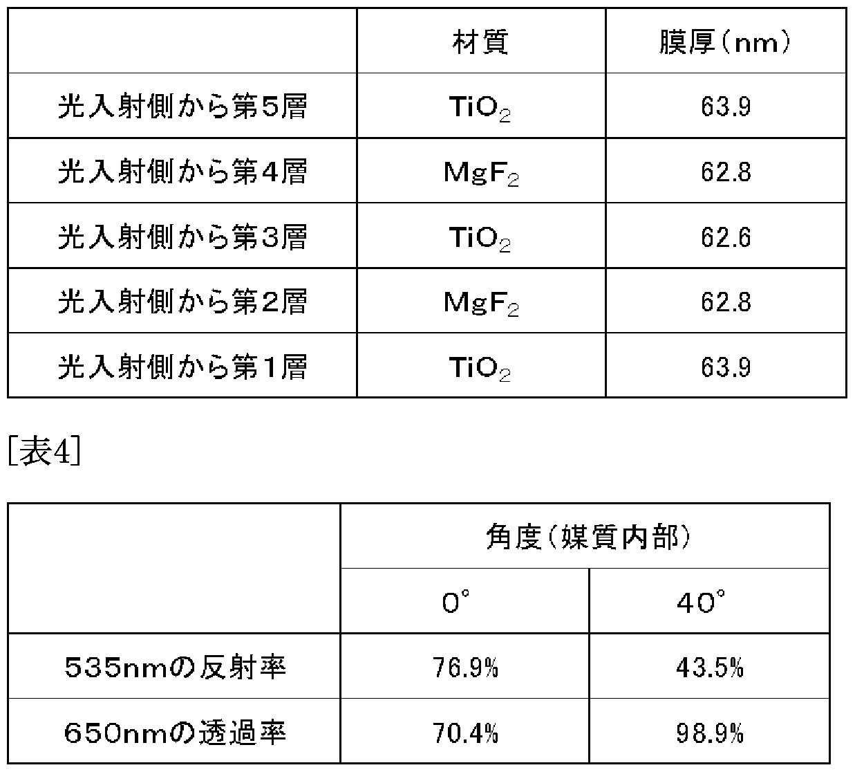
- the thickness was optimized to increase the reflectance at 535 nm and the transmittance at 650 nm.
- the refractive index of the medium is 1.52.
- 'Wavelength was calculated with 535nm recording and 650nm tracking. It is also possible to use a string of 535 nm and 780 nm tracking, 405 nm and 650 nm tracking, 405 nm recording and 78 Onm tracking, etc.
- Tables 1 and 2 and Figure 9 show the simulation results when three layers of dielectric thin films are stacked.
- Tables 5 and 6 and Fig. 11 show the simulation results when seven dielectric thin films are stacked.
- a base vinylome coated with polyvinyl alcohol (trade name MP203, manufactured by Kuraray Co., Ltd.) to a thickness of 1 ⁇ m on a polycarbonate film (product name: Iupilon, manufactured by Mitsubishi Gas Engineering Co., Ltd.) having a thickness of 100 m.
- a colorant-containing layer coating solution having the following composition was prepared by a conventional method.
- the color material-containing layer coating solution was applied onto the base film with a bar coater and dried to produce a base film having a color material-containing layer having a thickness of 3 m.
- Cube produced a dielectric deposited filter with three layers in the same manner as in the simulation with the above three layers.
- the optical recording medium filter of Example 2 is the same as Example 1 except that a dielectric-deposited filter having 5 layers is produced in the same manner as in the simulation in the case of 5 layers in Example 1. Was made.
- Example 1 the optical recording of Example 3 was performed in the same manner as in Example 1 except that a dielectric-deposited filter having 7 layers was produced in the same manner as in the simulation in the case of 7 layers.
- a filter for recording media was prepared.
- the optical recording medium filter of Example 4 was made in the same manner as in Example 1 except that a dielectric-deposited filter having 9 layers was produced in the same manner as in the simulation in the case of the above 9-layer lamination in Example 1. Was made.
- the filters for optical recording media of Examples 1 to 4 can reflect 30% or more of 532 nm light, which is the selected wavelength, for light within an incident angle of ⁇ 40 ° as shown in FIGS. It was recognized that
- a general polycarbonate resin substrate used for DVD + RW having a diameter of 120 mm and a thickness of 0.6 mm was used as the lower substrate.
- a servo pit pattern is formed on the entire surface of the substrate, the track pitch is 0.74 m, the groove depth is 175 nm, and the groove width is 300 nm.
- a reflective film was formed on the servo pit pattern surface of the lower substrate.
- Aluminum (A1) was used as the reflective film material.
- the A1 reflective film with a thickness of 200 ⁇ m was formed by DC magnetron sputtering.
- the dielectric vapor deposition filter produced in Example 1 was punched into a predetermined disk size so that it could be placed on the lower substrate, and the base film surface was set to the servo pit pattern side. And the thickness was adjusted so that the color material-containing layer had a thickness of 40 m.
- a filter layer was formed as described above.
- the obtained photopolymer coating solution is placed on the filter layer using a dispenser, and the end of the disk is pressed onto the photopolymer while pressing a polycarbonate resin upper substrate having a diameter of 12 cm and a thickness of 0.6 mm. And the upper substrate were bonded with an adhesive. Note that a flange portion is provided at the end of the disk so that the photopolymer layer has a thickness of 500 m. The thickness of the photopolymer layer is determined by bonding the upper substrate to the flange. New photopolymer overflows and is removed. Thus, the optical recording medium of Example 5 was produced.
- Example 5 except that the dielectric vapor deposition filter produced in Example 1 was replaced with the dielectric vapor deposition filter produced in Example 2, and the thickness of the colorant-containing layer was adjusted to 30 m.
- An optical recording medium of Example 6 was produced in the same manner as Example 5.
- Example 5 except that the dielectric vapor deposition filter produced in Example 1 was replaced with the dielectric vapor deposition filter produced in Example 3, and the thickness of the colorant-containing layer was adjusted to 20 m.
- An optical recording medium of Example 7 was produced in the same manner as Example 5.
- Example 5 Production of one optical recording medium In Example 5, except that the dielectric vapor deposition filter produced in Example 1 was replaced with the dielectric vapor deposition filter produced in Example 4, and the thickness of the colorant-containing layer was adjusted to 10 m.
- the optical recording medium of Example 8 was produced in the same manner as Example 5.
- Example 7 the optical recording medium of Example 9 was produced in the same manner as in Example 7 except that the second gap layer was provided between the reflective film and the filter layer.
- the second gap layer a polycarbonate film having a thickness of 100 m was used and adhered with an ultraviolet curable resin.
- Example 7 an optical recording medium of Comparative Example 1 was produced in the same manner as Example 7 except that the filter layer (coloring material-containing layer + dielectric deposited film) was not formed.
- Example 8 the optical recording medium of Comparative Example 2 was produced in the same manner as in Example 8 except that the filter layer that did not form the colorant-containing layer was used on the dielectric vapor deposition filter produced in Example 1. did.
- the filter for optical recording media of the present invention can prevent the occurrence of noise that does not cause a shift in the selective reflection wavelength even when the incident angle changes, and is a holographic type capable of recording unprecedented high-density images. It is suitably used as a wavelength selective reflection film in an optical recording medium.
- the optical recording medium of the present invention is capable of preventing the occurrence of noise without causing a shift in the selective reflection wavelength even when the incident angle changes, and various holographic optical recording media capable of recording an unprecedented high-density image. Widely used.
Landscapes
- Physics & Mathematics (AREA)
- General Physics & Mathematics (AREA)
- Holo Graphy (AREA)
- Optical Record Carriers And Manufacture Thereof (AREA)
- Optical Recording Or Reproduction (AREA)
Abstract
Description






Claims
Priority Applications (1)
| Application Number | Priority Date | Filing Date | Title |
|---|---|---|---|
| EP05809197A EP1830355A1 (en) | 2004-12-03 | 2005-11-24 | Optical recording medium filter, optical recording medium, its manufacturing method, optical recording method, and optical reproducing method |
Applications Claiming Priority (2)
| Application Number | Priority Date | Filing Date | Title |
|---|---|---|---|
| JP2004352084 | 2004-12-03 | ||
| JP2004-352084 | 2004-12-03 |
Publications (1)
| Publication Number | Publication Date |
|---|---|
| WO2006059531A1 true WO2006059531A1 (ja) | 2006-06-08 |
Family
ID=36564965
Family Applications (1)
| Application Number | Title | Priority Date | Filing Date |
|---|---|---|---|
| PCT/JP2005/021583 Ceased WO2006059531A1 (ja) | 2004-12-03 | 2005-11-24 | 光記録媒体用フィルタ、光記録媒体及びその製造方法、並びに光記録方法及び光再生方法 |
Country Status (2)
| Country | Link |
|---|---|
| EP (1) | EP1830355A1 (ja) |
| WO (1) | WO2006059531A1 (ja) |
Citations (6)
| Publication number | Priority date | Publication date | Assignee | Title |
|---|---|---|---|---|
| JPS61248231A (ja) * | 1985-04-25 | 1986-11-05 | Ricoh Co Ltd | 光記録方法および光記録媒体 |
| JPS63101869A (ja) * | 1986-10-17 | 1988-05-06 | Konica Corp | カラ−画像形成装置 |
| JP2002063738A (ja) * | 2000-06-09 | 2002-02-28 | Tdk Corp | 光情報媒体 |
| JP2002117585A (ja) * | 2000-06-09 | 2002-04-19 | Tdk Corp | 光情報媒体 |
| JP2004265472A (ja) * | 2003-02-06 | 2004-09-24 | Optware:Kk | 光情報記録媒体 |
| JP2004280953A (ja) * | 2003-03-17 | 2004-10-07 | Hitachi Ltd | 光ディスクへの視認情報記録方法 |
-
2005
- 2005-11-24 WO PCT/JP2005/021583 patent/WO2006059531A1/ja not_active Ceased
- 2005-11-24 EP EP05809197A patent/EP1830355A1/en not_active Withdrawn
Patent Citations (6)
| Publication number | Priority date | Publication date | Assignee | Title |
|---|---|---|---|---|
| JPS61248231A (ja) * | 1985-04-25 | 1986-11-05 | Ricoh Co Ltd | 光記録方法および光記録媒体 |
| JPS63101869A (ja) * | 1986-10-17 | 1988-05-06 | Konica Corp | カラ−画像形成装置 |
| JP2002063738A (ja) * | 2000-06-09 | 2002-02-28 | Tdk Corp | 光情報媒体 |
| JP2002117585A (ja) * | 2000-06-09 | 2002-04-19 | Tdk Corp | 光情報媒体 |
| JP2004265472A (ja) * | 2003-02-06 | 2004-09-24 | Optware:Kk | 光情報記録媒体 |
| JP2004280953A (ja) * | 2003-03-17 | 2004-10-07 | Hitachi Ltd | 光ディスクへの視認情報記録方法 |
Also Published As
| Publication number | Publication date |
|---|---|
| EP1830355A1 (en) | 2007-09-05 |
Similar Documents
| Publication | Publication Date | Title |
|---|---|---|
| WO2007026483A1 (ja) | 光記録方法、光記録装置、光記録媒体及び光記録再生方法 | |
| WO2007088972A1 (ja) | 光記録再生装置、光記録方法、及び光再生方法 | |
| US7894319B2 (en) | Optical recording medium, method of producing the same, and, optical recording method and optical reproducing method | |
| WO2007072882A1 (ja) | 光記録媒体、並びに光記録装置、光記録方法及び光再生方法 | |
| JP2006301171A (ja) | 光記録媒体及びその製造方法、並びに、光記録媒体の記録方法及び光記録媒体の再生方法 | |
| WO2007043300A1 (ja) | 光記録媒体用フィルタ及びその製造方法、並びに光記録媒体及びその記録方法及び再生方法 | |
| WO2006059515A1 (ja) | 光記録媒体用フィルタ、光記録媒体及びその製造方法、並びに光記録方法及び光再生方法 | |
| JP2007102185A (ja) | 光記録媒体及びその製造方法、並びに、光記録方法及び光再生方法 | |
| JP2007079164A (ja) | 光記録媒体及びその製造方法、並びに、光記録装置及び光再生装置 | |
| JP2006301127A (ja) | 光記録媒体及びその製造方法、並びに、光記録媒体の記録方法及び光記録媒体の再生方法 | |
| JP4373383B2 (ja) | 光記録方法、光記録装置、光記録媒体及び光記録再生方法 | |
| WO2006059516A1 (ja) | 光記録媒体用フィルタ、光記録媒体及びその製造方法、並びに光記録方法及び光再生方法 | |
| JP2007004879A (ja) | 光記録方法、光記録装置及び光記録媒体 | |
| WO2007097352A1 (ja) | 光記録方法、光再生方法、光記録装置、及び光記録媒体 | |
| WO2006112106A1 (ja) | 光記録媒体用フィルタ、光記録媒体及びその製造方法、並びに、光記録方法及び光再生方法 | |
| WO2006059531A1 (ja) | 光記録媒体用フィルタ、光記録媒体及びその製造方法、並びに光記録方法及び光再生方法 | |
| JP2007003692A (ja) | 光記録方法、光記録装置及び光記録媒体 | |
| JP4724568B2 (ja) | 光記録媒体及びその製造方法 | |
| JP2006184897A (ja) | 光記録媒体用フィルタ、光記録媒体及びその製造方法、並びに光記録方法及び光再生方法 | |
| WO2007023635A1 (ja) | 光記録方法、光記録装置、光記録媒体及び光記録再生方法 | |
| WO2006059517A1 (ja) | 光記録媒体用フィルタ、光記録媒体及びその製造方法、並びに光記録方法及び光再生方法 | |
| JP2007066462A (ja) | 光記録再生装置及び光記録媒体の記録再生方法 | |
| JP2007132988A (ja) | 光記録媒体及びその製造方法、並びに光記録媒体の記録方法及びその再生方法 | |
| JP4751699B2 (ja) | 光記録媒体及びその製造方法 | |
| JP2007257800A (ja) | 光記録方法及び光再生方法、並びに光記録装置及び光再生装置 |
Legal Events
| Date | Code | Title | Description |
|---|---|---|---|
| AK | Designated states |
Kind code of ref document: A1 Designated state(s): AE AG AL AM AT AU AZ BA BB BG BR BW BY BZ CA CH CN CO CR CU CZ DE DK DM DZ EC EE EG ES FI GB GD GE GH GM HR HU ID IL IN IS JP KE KG KM KN KP KR KZ LC LK LR LS LT LU LV LY MA MD MG MK MN MW MX MZ NA NG NI NO NZ OM PG PH PL PT RO RU SC SD SE SG SK SL SM SY TJ TM TN TR TT TZ UA UG US UZ VC VN YU ZA ZM ZW |
|
| AL | Designated countries for regional patents |
Kind code of ref document: A1 Designated state(s): BW GH GM KE LS MW MZ NA SD SL SZ TZ UG ZM ZW AM AZ BY KG KZ MD RU TJ TM AT BE BG CH CY CZ DE DK EE ES FI FR GB GR HU IE IS IT LT LU LV MC NL PL PT RO SE SI SK TR BF BJ CF CG CI CM GA GN GQ GW ML MR NE SN TD TG |
|
| 121 | Ep: the epo has been informed by wipo that ep was designated in this application | ||
| NENP | Non-entry into the national phase |
Ref country code: DE |
|
| WWE | Wipo information: entry into national phase |
Ref document number: 2005809197 Country of ref document: EP |
|
| WWP | Wipo information: published in national office |
Ref document number: 2005809197 Country of ref document: EP |
|
| NENP | Non-entry into the national phase |
Ref country code: JP |