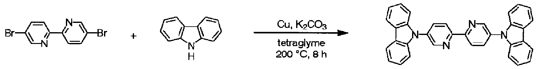
明 細 書
有機化合物、電荷輸送材料及び有機電界発光素子
発明の分野
[0001] 本発明は有機化合物及び電荷輸送材料と、この有機化合物を用いた有機電界発 光素子に関する。
発明の背景
[0002] 有機薄膜を用いた電界発光素子、即ち有機電界発光素子は、通常、基板上に、陽 極、陰極、及びこれら両極間に設けられた少なくとも発光層を含む有機層を有する。 有機層としては、発光層以外にも、正孔注入層(陽極バッファ層)、正孔輸送層、正 孔阻止層、電子輸送層、電子注入層等が設けられる。通常、これらの層を陽極と陰 極との間に積層することにより有機電界発光素子が構成されている。
[0003] 従来、有機電界発光素子は、蛍光発光を利用してきたが、素子の発光効率を上げ る試みで、蛍光ではなく燐光発光を用いることが検討されている。し力しながら、燐光 発光を用いた場合でも、未だ十分な発光効率が得られて!/、な 、のが現状である。
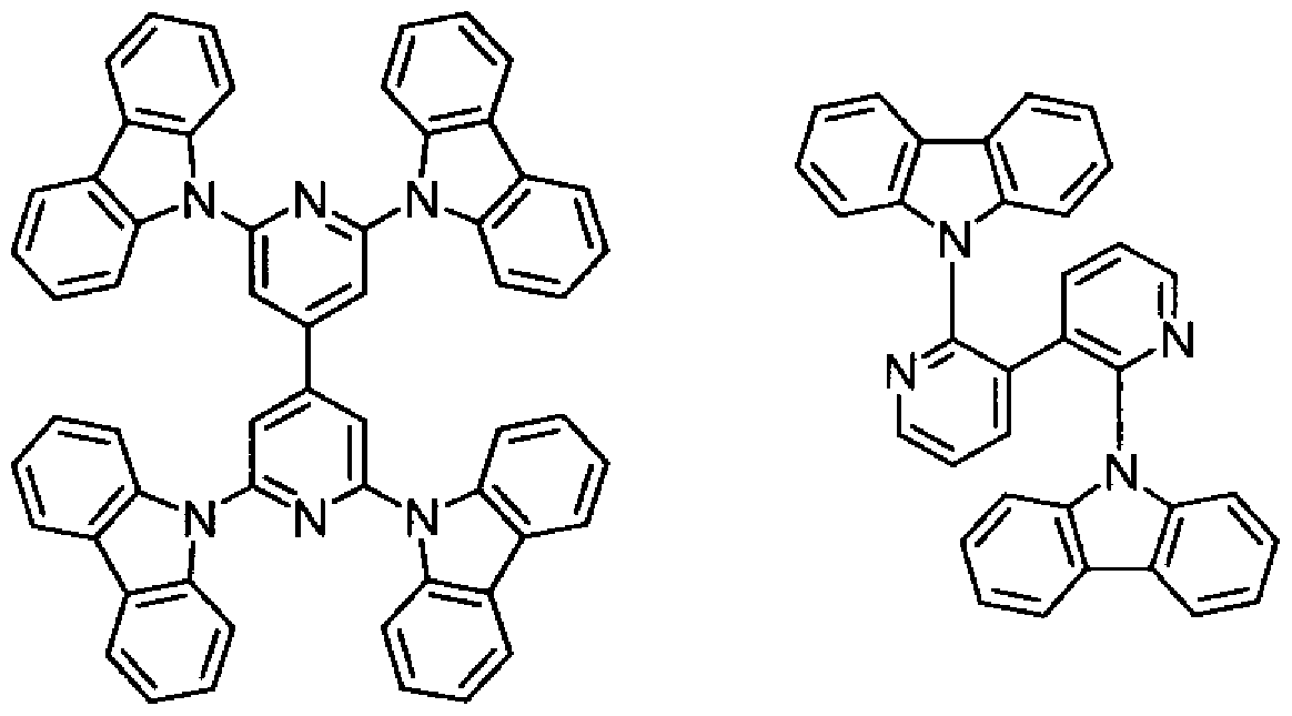
[0004] これまでに開発された燐光発光性分子を用いた有機電界発光素子の多くは、発光 層の材料 (ホスト材料)として、力ルバゾリル基を含む材料を用いることを特徴としてお り、例えば、非特許文献 1ではホスト材料として以下に示すビフエニル誘導体を用い ている。
[化 1]
し力しながら、上記ビフヱニル誘導体を用いた有機電界発光素子は、電荷の再結 合位置が陰極側に偏る傾向があり、バランスが取り辛ぐ高い発光効率が得られてい なかった。
下記特許文献 1には、再結合領域を発光層に集中させることが可能な、正孔輸送 性と電子輸送性を兼ね備えたホスト材料として、以下に示す化合物を有した有機電 界発光素子が記載されて!ヽる。
[化 2]
しかしながら、上記化合物は、ピリジン環を 1つしか有しておらず、 LUMOが 1つの ピリジン環に局在化しているため、電子輸送能が低ぐ更に、一電子還元されたとき の耐久性に問題がある。このため、該化合物は、高電圧下でしか発光が観測されず 、発光輝度、発光効率が不十分である。
また、特許文献 2には、有機電界発光素子の材料として、以下に示すィ匕合物などを 用いることが提案されている。
し力しながら、これらの化合物は、ピリジン環又はピラジン環を 1つしか有しておらず
、前述したように、電子輸送能及び一電子還元されたときの耐久性の点で改善の必 要がある。更に、窒素原子を同一の環に 2つ以上含むピラジン環やピリミジン環など を有する化合物は、ピリジン環を有する化合物に比べて、三重項励起準位が低ぐ一 電子還元されたときの耐久性も低いと考えられるため、ホスト材料としては問題がある また、特許文献 2及び特許文献 3には、有機電界発光素子の材料として、以下に示 すィ匕合物などを用いることが提案されて 、る。
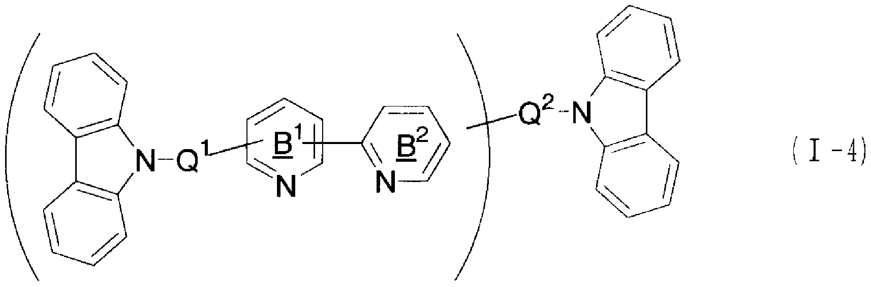
[化 4]
これらの化合物は、直接結合された 2つのピリジン環 (ビビリジル骨格)を有するため 、ある程度 LUMOが非局在化し、電子輸送能が若干改善されていると考えられる。 しかしながら、これらの化合物のピリジン環は、もう一方のピリジン環と直接結合してい る炭素原子の、両側のオルト位の炭素原子が、全て水素原子又は置換基に結合して いる。このため、立体障害により、これらの化合物のビビリジル骨格は平面性に乏しく 、 LUMOの非局在化が未だ不十分であり、電子輸送能に問題がある。更に、ビビリ ジル骨格は一電子還元されたときに平面性が高くなるため、ビビリジル骨格の平面性 が高くなりにくいこれらの化合物は、一電子還元されたときの耐久性に問題があり、実 用的な駆動寿命を達成し得な ヽ。
また、特許文献 2及び特許文献 4には、有機電界発光素子の材料として、以下に示 すィ匕合物などを用いることが提案されて 、る。
これらの化合物は、電子輸送能及び一電子還元されたときの耐久性は改善されて いることが予想されるものの、カルバゾリル基が一つだけであるため、正孔輸送性に 乏しぐ有機電界発光素子の発光層の材料としては、正孔輸送性と電子輸送性のバ ランスが悪ぐホスト材料としては改善が必要である。
特許文献 1:特開平 6— 1972号公報
特許文献 2:国際公開第 WO03Z078541号パンフレット
特許文献 3:特開 2004 -273190号公報
特許文献 4:国際公開第 WO03Z080760号パンフレット
非特許文献 l :Appl.Phys丄 ett.,75卷, 4頁, 1999年
発明の概要
[0009] 本発明は、優れた正孔輸送性と電子輸送性を併せ持ち、優れた電気的酸化還元 耐久性と高!ヽ三重項励起準位を有する有機化合物及び電荷輸送材料と、この有機 化合物を用いた、高!ヽ発光効率と高!ヽ駆動安定性を有する有機電界発光素子を提 供することを課題とする。
[0010] 本発明の第 1アスペクトの有機化合物は、下記式 (I)で表される。
本発明の第 2アスペクトの電荷輸送材料は、第 1アスペクトの有機化合物を含有す る。
本発明の第 3アスペクトの有機電界発光素子は、基板上に、陽極、陰極、及びこれ ら両極間に設けられた有機発光層を有し、さらに、該陽極と陰極との間に、第 1ァス
ぺタトの有機化合物を含有してなる層を有する。
[化 6] Q
2_Cz
2 ( )
式中、 Cz
1及び Cz
2は、力ルバゾリル基を表す。 Cz
1及び Cz
2は同一であっても異な つていても良い。
Q1及び Q2は、直接結合又は任意の連結基を表す。 Q1及び Q2は同一であっても異 なっていても良い。
Q
2、環 B
1及び環 B
2は、それぞれ置換基を有していても良い。
図面の簡単な説明
[0011] [図 1]本発明の有機電界発光素子の一例を示した模式的断面図である。
[図 2]本発明の有機電界発光素子の別の例を示した模式的断面図である。
[図 3]本発明の有機電界発光素子の別の例を示した模式的断面図である。
発明の好ましレ、形態の詳細な説明
[0012] 第 1アスペクトの有機化合物は、高 ヽ三重項励起順位を有し、優れた電荷輸送性 ( 正孔輸送性、電子輸送性)、電気的酸化還元耐久性を有する。このため、この有機 化合物を用いた有機電界発光素子によれば、高輝度 ·高効率で発光させることが可 能となり、かつ素子の安定性、特に駆動安定性が向上し、長寿命化する。
[0013] 第 1アスペクトの有機化合物を用いた第 3アスペクトの有機電界発光素子は、フラッ トパネル'ディスプレイ (例えば OAコンピュータ用や壁掛けテレビ)、車載表示素子、 携帯電話表示や面発光体としての特徴を生力 た光源 (例えば、複写機の光源、液 晶ディスプレイや計器類のバックライト光源)、表示板、標識灯への応用が考えられ、 その技術的価値は大き 、ものである。
[0014] 第 1アスペクトの有機化合物は、本質的に優れた酸化還元安定性を有することから 、有機電界発光素子に限らず、電子写真感光体に利用することも有用である。
この有機化合物は、電荷輸送材料用としてだけでなぐ各種発光材料用、太陽電
池材料用、バッテリー材料 (電解液、電極、分離膜、安定剤など)用、医療用、塗料材 料用、コーティング材料用、有機半導体材料用、トイレタリー材料用、帯電防止材料 用、熱電素子材料用などにおいても有用である。
[0015] 第 2アスペクトの電荷輸送材料は、優れた成膜性、電荷輸送性、発光特性、耐熱性 から、素子の層構成に合わせて、正孔注入材料、正孔輸送材料、発光材料、ホスト 材料、電子注入材料、電子輸送材料などとしても適用可能である。
[0016] 以下に本発明の有機化合物、電荷輸送材料及び有機電界発光素子の好ま 、形 態を詳細に説明する。
[0017] 〔有機化合物〕
第 1アスペクトの有機化合物は、上記式 (I)で表される。
[0018] [1]構造上の特徴
上記式 (I)で表される本発明の有機化合物は、優れた酸化還元耐久性を有し、電 子輸送を主として担う部分と、正孔輸送を主として担う部分とをバランス良く有する。
[0019] 電子輸送を主として担う部分である環 B1—環 B2は、環 B2の N原子に水素原子又は 置換基が結合しておらず、環 、環 B2の間での立体障害が小さいため、平面性の高 いビビリジル骨格を形成する。これにより、環 B1—環 B2上に十分に LUMOが非局在 化するため、この有機化合物は、優れた電子輸送能を有する。基底状態と一電子還 元された状態との間の構造変化が小さいため、この有機化合物は、一電子還元され たときの耐久性に優れる。
[0020] 本発明の有機化合物はこのような特性を有するため、有機電界発光素子としたとき の素子駆動電圧が低減され、更に素子駆動安定性が向上する。
[0021] また、本発明の有機化合物は、正孔輸送を主として担う部分として、 Cz1— Q1—及 び Cz2— Q2—のように、力ルバゾリル基を 2以上有する。従って、この有機化合物は、 優れた正孔輸送能を有する。この有機化合物を有した有機電界発光素子は、素子 駆動電圧が低減され、正孔と電子が発光層中で再結合を起こすために必要な正負 電荷の供給バランスを取ることが容易である。
[0022] [2]式 (I)中の構成要素
〈環 B1及び環 B2〉
環 B1及び環 B2はピリジン環であり、互!、に独立に Cz1— Q1 或いは Cz2— Q 以 外にも任意の置換基を有していても良い。なお、環 B2は必ずしも Cz2— Q2 が置換 しているものではない。
式 (I)の部分構造である、下記式 (Γ)としては、下記式 (III— 1)、(III— 2)、又は(III 3)がある。これらのうち、 LUMOが非局在化している点から、式(III 1)及び式(II I 2)が好ましぐ平面性が高ぐ電子輸送能及び還元耐久性に優れることから、式 (I II 1)がより好ましい。
[化 7]
環 B
1及び/又は環 B
2が有しても良 、置換基としては、例えば、アルキル基、芳香 族炭化水素基、ァシル基、アルコキシ基、ァリールォキシ基、アルキルチオ基、ァリー ルチオ基、アルコキシカルボ-ル基、ァリールォキシカルボ-ル基、ハロゲン原子、 ァリールアミノ基、アルキルアミノ基、芳香族複素環基等が挙げられ、好ましくはアル キル基、芳香族炭化水素基、芳香族複素環基、より好ましくは、ベンゼン環、ナフタレ ン環、アントラセン環、フエナントレン環、ペリレン環、テトラセン環、ピレン環、ベンズ ピレン環、タリセン環、トリフエ-レン環、フルオランテン環、力ルバゾール環などの、 6 員環の単環又は 2〜5縮合環由来の 1価の基、或いは、それらが複数個連結されて
形成された 1価の基 (例えば、ビフヱ-ル基、ターフェニル基など)であり、更に好まし くは、フエ-ル基、 4ービフヱ-ル基、 3—力ルバゾリルフヱ-ル基、 4一力ルバゾリル フエ-ル基、 N—力ルバゾリル基である。
[0025] 環 B1及び Z又は環 B2が置換基を有する場合、もう一方のピリジン環と直接結合し ている炭素原子のメタ位又はパラ位に置換基を有することが好ましい。例えば、環 が置換基を有する場合には、 4位、 5位、 6位の何れかに置換基を有することが好まし い。
[0026] 即ち、環 B1及び環 B2には、 Cz1— Q1—及び Cz2— Q2—も含め、それぞれ最大で合 計 5つの置換基が置換可能であるが、もう一方のピリジン環と直接結合している炭素 原子のオルト位に置換基を有する場合、置換基を有さな ヽ (水素原子を有する)場合 に比べ、立体障害が大きぐ電子輸送能及び還元耐久性が低下するため、環 B1及 び環 B2に、もう一方のピリジン環と直接結合している炭素原子のオルト位に置換基を 有さないことが好ましい。
[0027] ただし、環 B1及び環 B2は、 Cz1— Q1—及び Cz2— Q2—以外に置換基を有さないこ と、或いは、環 B1及び/又は環 B2がフエ-ル基、 3—力ルバゾリルフヱ-ル基を置換 基として有することが好ましぐ最も好ましくは、環 B1及び環 B2が Cz1— Q1—及び Cz2 — Q2—以外に置換基を有さないことである。
[0028] 即ち、環 B1及び/又は環 B2に、 Cz1— Q1—及び Cz2— Q2—以外の置換基を有す る場合、 Cz1— Q1—及び Cz2-Q2—のみしか置換基を有さない場合に比べ、一電子 還元された際に、負電荷が遮蔽されて電子輸送能が低下するため、環 B1及び Z又 は環 B2に、 Cz1— Q1—及び Cz2— Q2—以外に置換基を有さないこと、特に、環 B1及 び環 B2が Cz1— Q1—及び Cz2— Q2—以外に置換基を有さな 、ことが好まし 、。
[0029] く Cz1及び Cz2〉
Cz1及び Cz2は、それぞれ力ルバゾリル基を表す。
Cz1及び Cz2は、同一であっても異なって!/、ても良!、。
Cz1及び Cz2としては、 N—力ルバゾリル基、 1一力ルバゾリル基、 2—力ルバゾリル 基、 3—力ルバゾリル基、 4一力ルバゾリル基が挙げられる。高い三重項励起準位、優 れた電気化学的安定性の観点から、 N—力ルバゾリル基又は 2—力ルバゾリル基が
好ましく、 N カルバゾリル基が最も好まし 、。
[0030] 式 (I)における Cz1及び Cz2が N—力ルバゾリル基である場合の式 (I)を、下記式 (I
4)に示す。
[化 8]
[0031] Cz1及び Cz2は、各々独立に、任意の置換基を有していても良い。
該置換基として好ましくは、アルキル基、芳香族炭化水素基、ァシル基、アルコキシ 基、ァリールォキシ基、アルキルチオ基、ァリールチオ基、アルコキシカルボ-ル基、 ァリールォキシカルボ-ル基、ハロゲン原子、ァリールアミノ基、アルキルアミノ基、芳 香族複素環基であり、より好ましくはアルキル基、芳香族炭化水素基、芳香族複素環 基である。
[0032] 高 、三重項励起準位の観点、電荷分布の偏りに伴う電気的耐性の低下を避ける観 点から、この置換基は、好ましくは、ベンゼン環、ナフタレン環、アントラセン環、フエ ナントレン環、ペリレン環、テトラセン環、ピレン環、ベンズピレン環、タリセン環、トリフ ェニレン環、フルオランテン環などの、 6員環の単環又は 2〜5縮合環由来の 1価の基 、或いは、それらが複数個連結されて形成された 1価の基 (例えば、ビフヱ-レニル基 、ターフェ-レニル基など)である。
[0033] Cz1及び Cz2それぞれの置換基は、合計で分子量 500以下が好ましぐ 250以下が 更に好ましい。最も好ましくは Cz1及び Cz2は無置換であることである。
[0034] 尚、本発明の有機化合物は、分子中に存在する全てのカルバゾリル基が下記式 (II )で表される N—力ルバゾリル基であることが好まし 、。
[0035] く Q1及び Q2〉
Q1及び Q2は、直接結合或いは任意の連結基を表す。
Q1及び Q2は同一であっても異なって ヽても良 、。
[0036] 任意の連結基としては、ベンゼン環、ナフタレン環、アントラセン環、フエナントレン 環、ペリレン環、テトラセン環、ピレン環、ベンズピレン環、タリセン環、トリフエ-レン環 、フルオランテン環などの、 6員環の単環又は 2〜5縮合環由来の 2価の連結基、或 いは、それらが複数個連結されて形成された 2価の連結基 (例えば、ビフエ二レン基、 ターフェ-レン基など)が好ましく挙げられる。 Q1及び Q2として、好ましくは、直接結 合又は、フエ-レン基、ビフエ-レン基、ターフェ-レン基などのベンゼン環を 1〜8個 連結してなる 2価の連結基である。
[0037] Q1及び Q2が任意の連結基である場合、 Q1及び Q2は、各々独立に、任意の置換基 を有していても良ぐ該置換基としては好ましくは、アルキル基、芳香族炭化水素基、 ァシル基、アルコキシ基、ァリールォキシ基、アルキルチオ基、ァリールチオ基、アル コキシカルボ-ル基、ァリールォキシカルボ-ル基、ハロゲン原子、ァリールアミノ基 、アルキルアミノ基、芳香族複素環基であり、より好ましくはアルキル基、芳香族炭化 水素基、芳香族複素環基であり、特に好ましくは、ベンゼン環、ナフタレン環、アント ラセン環、フエナントレン環、ペリレン環、テトラセン環、ピレン環、ベンズピレン環、タリ セン環、トリフエ-レン環、フルオランテン環などの、 6員環の単環又は 2〜5縮合環由 来の 1価の基、或いは、それらが複数個連結されて形成された 1価の基 (例えば、ビ フエ-レニル基、ターフェ-レニル基など)である。
[0038] Q1及び Q2は、それぞれ、分子量が 1000以下であることが好ましく、 500以下であ ることが更に好ましい。
[0039] Q1及び Q2は、特に、それぞれ、直接結合又は—(Ph) —であることが好ましい。こ
P
こで、 Phは置換基を有していても良いフエ-レン基を表す。また、 pは 1〜8の整数を 表し、好ましくは 1〜3の整数である。フエ-レン基の置換基としては、上記 Q1及び Q2 の置換基として例示したものと同様である。
尚、式 (I)において、 Q2は、環 、環 B2、 Q1及び Cz1のいずれに連結しても良いこと を示す。
[0040] く Cz1— Q1—及び Cz2— Q2—〉
Cz2、 Q1及び Q2については前述した力 Cz1と Q1及び Cz2と Q2の好ましい組 み合わせについて以下に説明する。
Cz1— Q1—及び Cz2— Q2—の好まし 、態様としては、次の [1]〜 [3]が挙げられる
[0041] [1] Cz1— Q1—及び Cz2— Q2—は、それぞれ下記式 (IV— 1)で表されることが好ま しい。以下、 Cz1— Q1—及び Cz2— Q2—を総称して、 Cz— Q—という。
[化 10]
環 Aは、ベンゼン環を表す。環 Aは置換基を有していても良い。
G及び G'は、それぞれ直接結合或いは任意の連結基を表す。 G及び G'は同一で あっても異なっていても良い。 G及び G'は置換基を有していても良い。
[0042] 式 (IV— 1)で表される Cz— Q—を有する有機化合物では、正孔輸送を主として担う 部分 (カルバゾリル基)と電子輸送を主として担う部分 (ビビリジル骨格)がベンゼン環 を介してメタ位で結合して 、る。式 (IV— 1 )で表される Cz -Q-を有する有機化合物 は、ベンゼン環の有する優れた耐熱性、優れた電気化学的安定性、高い三重項励 起準位によって、優れた電気化学的安定性、優れた耐熱性、高い三重項励起準位 を有する。式 (IV— 1)で表される Cz— Q—を有する有機化合物では、 m—連結型の
ベンゼン環は、電子受容性と電子供与性の両方を併せ持つため、カルバゾリル基が 酸化された場合には、必要に応じて正電荷の一部を受容し、環 , B2が還元された 場合には、必要に応じて負電荷の一部を受容する。これにより、式 (IV— 1)で表され る Cz— Q—を有する有機化合物は、酸ィ匕還元耐久性が更に向上する。
[0043] 式 (IV— 1)における G及び G'は、式 (I)における Qの一部分であり、好ましい例及 び有しても良い置換基の例は、式 (I)における Q1, Q2について前述したものと同様で ある。
[0044] 式 (IV— 1)における環 Aは、式 (I)における Q1, Q2の一部分であり、有しても良い置 換基の例は、式 (I)における Q1, Q2について前述したものと同様である。
[0045] 式 (IV— 1)で表される部分構造の分子量としては、好ましくは 2000以下、更に好ま しくは 1000以下である。
[0046] Cz1— Q1—及び Cz2-Q2—が上記式 (IV— 1)で表される場合、本発明の有機化合 物は、下記式 (1—1)であることが好ましい。
[化 11]
式中、 Gi Tは、式 (IV— 1)の G或いは G'と同義であり、直接結合又は任意の連 結基を表す。 Gi G
4はそれぞれ同一であっても異なって 、ても良 、。
環 A1及び環 A2は、式 (IV— 1)の環 Aと同義であり、ベンゼン環を表す。環 A1及び環 A2は、それぞれ置換基を有して!/ヽても良!、。
Cz2、環 B1及び環 B2は、式 (I)におけると同義である。
[0047] [2] Cz
1— Q
1—及び Cz
2— Q
2—は、結合して、下記式 (IV— 2)で表される部分構造 となることが好ましい。
式中、 Cz
1及び Cz
2は、式 (I)におけると同義である。
G5は、直接結合又は任意の連結基を表す。
Zは、 Cz1及び Cz2上の窒素原子同士を共役可能とする任意の連結基を表す。 G5及び Zは、それぞれ置換基を有していても良い。
[0048] Cz1及び Cz2は上記式(IV— 2)で表される、即ち、連結基 Zを介して二つの力ルバ ゾリル基上の窒素原子同士が共役可能であることが重要である。
[0049] 即ち、同一の芳香族炭化水素基 (この芳香族炭化水素基には、複数の環が連結さ れたもの(例えば、ビフエ-ル基)を含む)上に複数のカルバゾリル基が連結されて ヽ る場合、互いの窒素原子同士が非共役であると、電気的酸化を受けたとき、該芳香 族炭化水素基上に過剰の正電荷が集中し、或いは、カルバゾリル基の N, 1, 3, 6, 8—位の少なくとも一力所への正電荷の局在化が強まり、該電気的酸ィ匕に対する耐 久性が著しく低下してしまうため、好ましくない。
[0050] 他方、同一の芳香族炭化水素基 (この芳香族炭化水素基には、複数の環が連結さ れたもの(例えば、ビフエ-ル基)を含む)上に 2つのカルバゾリル基が連結されて!ヽ る場合、互いの窒素原子同士が共役可能であると、該芳香族炭化水素基及び 2つの カルバゾリル基上に正電荷が比較的均等に分布し、一電子酸ィ匕されたときの耐久性 に優れるため、好ましい。
[0051] ここで、窒素原子同士が共役可能であるとは、窒素原子同士が、
(cis-, trans-の ヽずれでも可)又はこれらを組み合わせてなる部分構造で連結されて いることと同義である。ただし、 Ga, Gb, Geは各々独立に、水素原子又は任意の置換 基を表すか、或いは、芳香族炭化水素環や芳香族複素環の一部を構成する。
[0052] 連結基 Z上には、 Cz1及び Cz2を含めて、好ましくは、合計で 2〜5つ、より好ましくは 2又は 4つ、最も好ましくは 2つである。
[0053] 式 (IV— 1)における Zは、式 (I)における Q1, Q2の一部分であるので、具体例及び 有しても良い置換基の例は、式 (I)における Q1, Q2について前述したものと同様であ る。但し、 Zは Cz1及び Cz2上の窒素原子同士を共役可能とする任意の連結基である
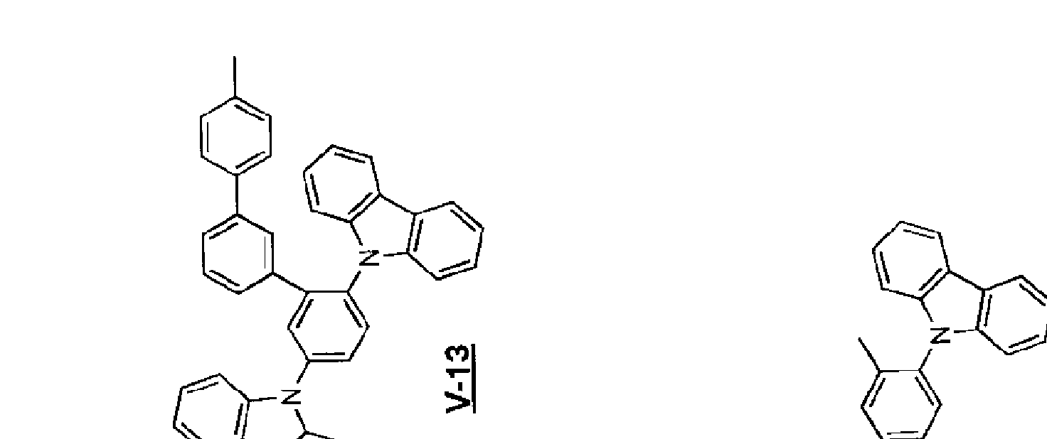
[0054] Zを含めた部分構造式 (IV— 2)としては以下のものが挙げられる。
[0055] [化 14]
[0056] [化 15]
l.00C/900Zdf/X3d 91· 6H080/900Z OAV
[0057] [化 16]
[0058] [化 17]
l.00C/900Zdf/X3d 81· 6H080/900Z OAV
[0059] 上記例示のうち、中でも、 V— 1, 2, 4〜15, 17〜21, 27, 28力 り好ましく、 V—
1, 6〜9, 11〜15力更に好ましく、 V— 1力最も好まし!/、。
[0060] 式 (IV— 2)における G5は、式 (I)における Q1, Q2の一部分であり、好ましい例及び 有しても良い置換基の例は、式 (I)における Q1, Q2について前述したものと同様であ る。
[0061] なお、式 (IV— 2)で表される部分構造の分子量としては、好ましくは 3000以下、更 に好ましくは 1500以下である。
[0062] Cz1— Q1—及び Cz2-Q2—が上記 (IV— 2)で表される場合、本発明の有機化合物 は下記式 (I 2)で表されることが好まし 、。
[化 18]
G5は、上記式 (IV— 2)の G5と同義であり、直接結合又は任意の連結基を表す。 Zは、上記式 (IV— 2)の Zと同義であり、 Cz1及び Cz2上の窒素原子同士を共役可 能とする任意の連結基を表す。 Zは置換基を有して 、ても良 、。
環 B
1及び環 B
2は、式 (I)におけると同義である。
[0063] [3] Cz1— Q1—及び Cz2— Q2—は、それぞれ環 B1及び B2に直接結合することが好 ましい。
この場合、本発明の有機化合物は、下記式 (1— 3)で表されることが、一電子酸化さ れたとき、正電荷がより広く分布するため、より優れた正孔輸送能を有し、ビビリジル 骨格の優れた電子輸送能とのバランスを取ることが容易になる点で好まし 、。
[0064] 式中、
環 B
1及び環 B
2は、式 (I)におけると同義である。
[0065] [3]分子量
本発明の有機化合物の分子量は、通常 4000以下、好ましくは 3000以下、より好ま しくは 2000以下であり、また通常 200以上、好ましくは 300以上、より好ましくは 400 以上である。
本発明の有機化合物の分子量がこの上限値を超えると、昇華性が著しく低下して 電界発光素子を制作する際に蒸着法を用いる場合において支障を来したり、不純物 の高分子量ィ匕によって精製が困難となる場合があり、またこの下限値を下回ると、ガ ラス転移温度及び、融点、気化温度などが低下するため、耐熱性が著しく損なわれる おそれがある。
[0066] [4]物性
本発明の有機化合物は、通常 50°C以上のガラス転移温度を有するが、有機電界 発光素子に使用する際には、その耐熱性の観点から、ガラス転移温度は 90°C以上 であることが好ましぐ 110°C以上であることが更に好ましい。ガラス転移温度の上限 は通常 400°C程度である。
本発明の有機化合物は、常圧下で通常 800°C以下の気化温度を有するが、有機 電界発光素子に使用する際には、その蒸着製膜工程の安定性の観点から、気化温 度は 700°C以下であることが好ましぐ 600°C以下であることが更に好ましい。気化温 度の下限は通常 300°C程度である。
本発明の有機化合物は、通常 100°C以上の融点を有するが、有機電界発光素子 に使用する際には、その耐熱性の観点から、融点は 150°C以上であることが好ましく 、 200°C以上であることが更に好ましい。融点の上限は通常 500°C程度である。
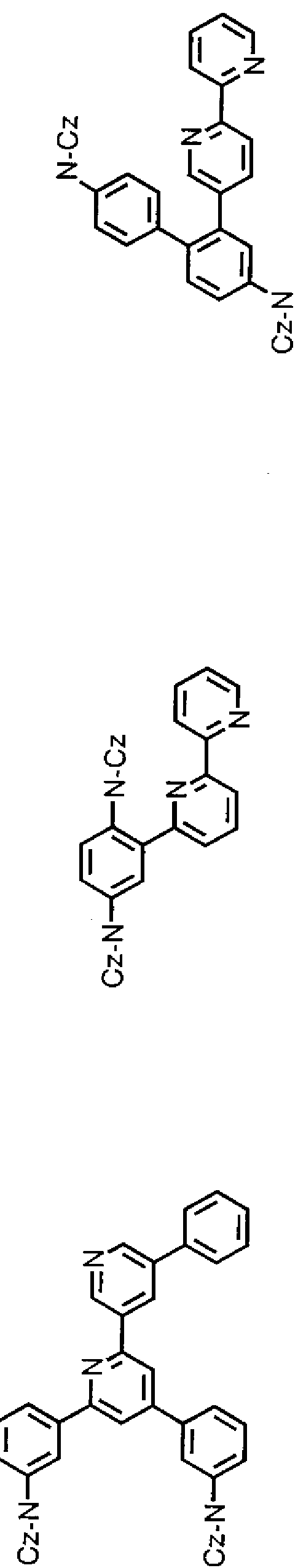
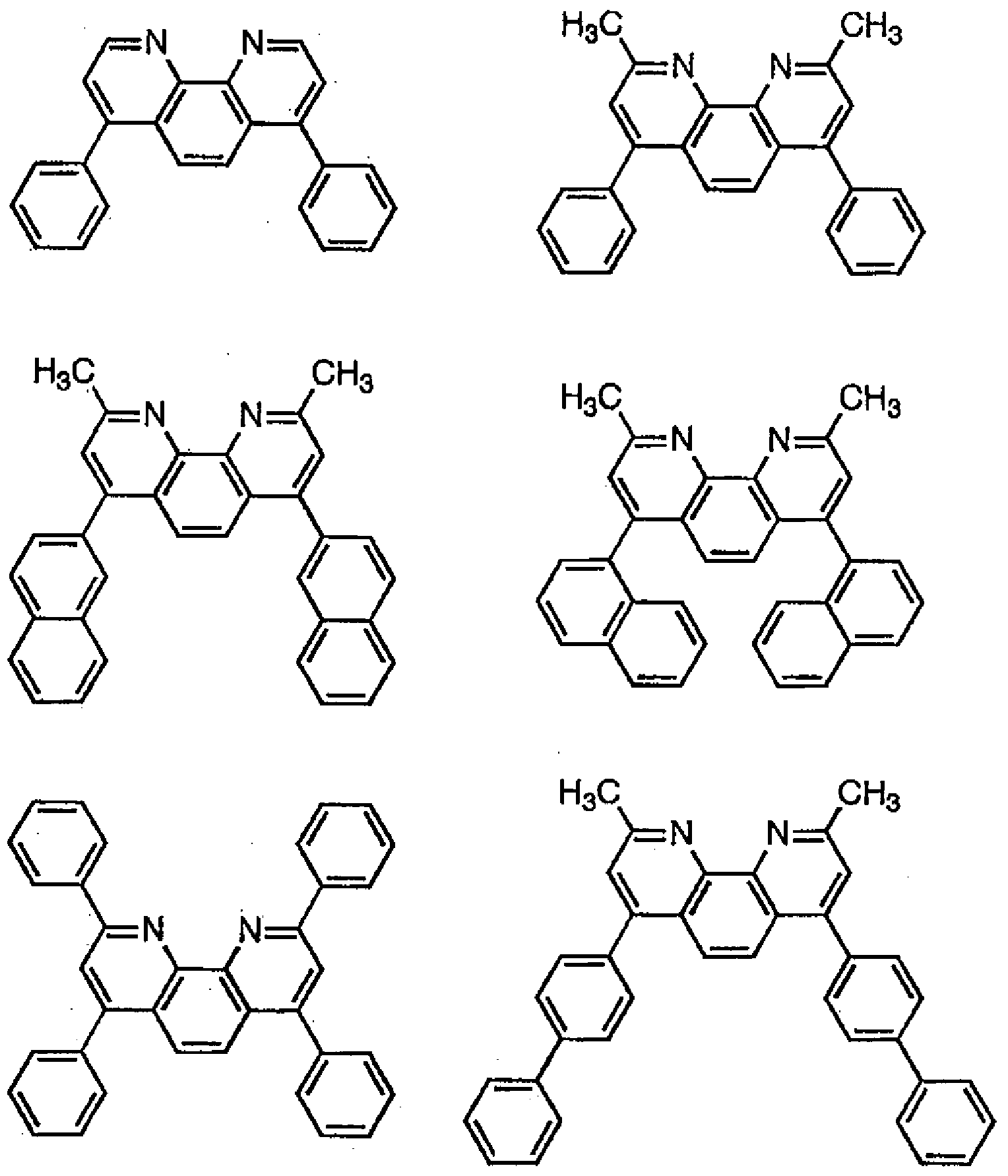
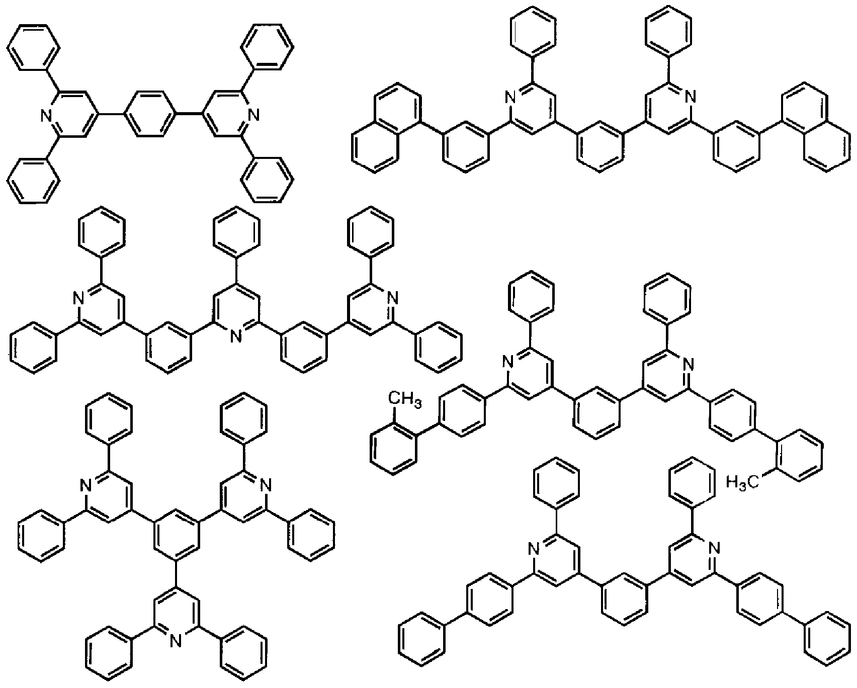
[0067] [5]具体例
以下に、本発明の有機化合物として好ましい具体的な例を示すが、本発明はこれ
らに限定されるものではない。なお、以下の例示構造式中、 N— Czは、 N 力ルバ ゾリル基を示す。
[化 20]
[0069] [化 21]
[0070] [化 22]
〔〕〔S00742
[0076] [6]合成法
本発明の有機化合物は、目的とする化合物の構造に応じて原料を選択し、公知の 手法を用いて合成することができる。
[0077] (1) まず、直接結合された 2つのピリジン環 (ビビリジル骨格)の導入方法としては、 次の A)ないし E)に記載の方法を採用することができる。
[0078] A) Synthesis,l-24;1976やその引用文献などで開示されている、アルデヒドとピリジ ルァセチリドとを、硫酸などの強酸存在下で酢酸、アルコール、ニトロベンゼンなどの 芳香族溶媒などの単独又は混合溶媒中で反応させて、或いは水酸ィ匕ナトリウムなど の強塩基存在下でアルコール及び Z又は水溶媒中で加熱条件下反応させて、中間
体(一 CH = CR— CO—)を得、これを酢酸、メタノールなどの溶媒中、加熱条件下、 酸素存在下、ァシルピリジ-ゥム塩と酢酸アンモ-ゥムを作用させて合成する方法。
[化 28]
[0079」 B) Synthesis, 1-24;1976やその引用文献、 Journal of the American Chemical So ciety, 126,4958-4971 ;2004, Inorganic Chemistry,42,2908- 2918;2003、 European Jo urnal of Inorganic Chemistry,1019-1029;2001などで開示されている、アルデヒドと ァセチリドとを、硫酸などの強酸存在下で酢酸、アルコール、ニトロベンゼンなどの芳 香族溶媒などの単独又は混合溶媒中で反応させて、或いは水酸ィ匕ナトリウムなどの 強塩基存在下でアルコール及び Z又は水溶媒中で加熱条件下反応させて、中間体 (一 CH=CR— CO—)を得、これを酢酸、メタノールなどの溶媒中、加熱条件下、酸 素存在下、ピリダシルピリジ-ゥム塩と酢酸アンモ-ゥムを作用させて合成する方法。
[化 29]
[0080] C) Synthesis,l- 24;1976やその引用文献、 Inorganic Chemistry,42,367-378;2002, Polyhedron,22,93-108;2003などで開示されている、アルデヒドと 1, 2—ジケトンとを、 硫酸などの強酸存在下で酢酸、アルコール、ニトロベンゼンなどの芳香族溶媒などの 単独又は混合溶媒中で反応させて、或いは水酸ィ匕ナトリウムなどの強塩基存在下で アルコール及び Z又は水溶媒中で加熱条件下反応させて、中間体(一 CH = CR— CO—) 2を得、これを酢酸、メタノールなどの溶媒中、加熱条件下、酸素存在下、ァ
シルピリジ-ゥム塩と酢酸アンモ-ゥムを作用させて合成する方法。
[化 30]
[0081] D) Journal of Organic Chemistry'67,443— 449;2002、 Inorganic Chemistry,42,36 7-378;2002などに開示されている、ハロゲン化ピリジンをパラジウム、ニッケルなどの 遷移金属触媒下でジスタナン、ジボランなどと反応させて、或いはハロゲンィ匕ピリジン をブチルリチウムなどの有機リチウム試薬と反応させた後、クロロスタナン、トリアルコ キシボランなどと反応させて、有機スズ試薬、有機ホウ素試薬、有機亜鉛試薬などの 有機金属試薬を得、これをパラジウム、ニッケルなどの遷移金属触媒下でハロゲンィ匕 ピリジンと反応させて合成する方法。
[化 31]
[0082] E) Tetrahedron,43,895— 904;1987、 Synthesis,321— 324;1998、 Organic Letters, 2, 80 3- 805;2000、 Journal of Organic Chemistry,67,443- 449;2002などに開示されてい るラネーニッケル、パラジウムカーボン、ブチルリチウム、三フッ化ボロンエーテル錯 体などを用いて、ピリジンをニ量ィ匕する方法。
[0083] (2) 次に、カルバゾリル基の導入方法としては、その結合位置により次のような方法 を採用することができる。
[0084] (2- 1) N—力ルバゾリル基の導入方法としては、次の a)〜c)に記載の方法を採用 することができる。
a)ビビリジル骨格を有する芳香族 2又は 2以上置換フッ化物 (F— Ar— F)と、置換 又は無置換の力ルバゾールと水素化ナトリウム、 tert—ブトキシカリウム、 n—ブチルリ
チウムなどの強塩基とを反応させたもの(フッ素原子に対して 1. 1〜10当量程度)と を、テトラヒドロフラン、ジォキサン、エーテル、 N, N—ジメチルホルムアミドなどの溶 液中で加熱還流下、 1〜60時間撹拌する方法。
[化 32]
b)ビビリジル骨格を有する芳香族 2又は 2以上置換ハロゲン化物 (X— Ar—X、好 ましくは X=Br, I)と、置換又は無置換の力ルバゾールとを、銅粉末、銅線、ハロゲン ィ匕銅 (CuX(X=Cl、 Br、 I) )、酸化銅 (CuO)などの銅触媒 (ハロゲン原子に対して 0 . 1〜5当量程度)及び、炭酸カリウム、炭酸カルシウム、リン酸カリウム、炭酸セシウム 、 tert -ブトキシナトリウムなど塩基性物質 (ハロゲン原子に対して 1〜 10当量程度) の存在下、不活性ガス気流下、無溶媒又は、ニトロベンゼンなどの芳香族溶媒、テト ラグライム、ポリエチレングリコールなどの溶媒中、 20〜300°Cの温度範囲で、 1〜6 0時間撹拌混合する方法。
[化 33]
[0086] c)ビビリジル骨格を有する芳香族 2又は 3置換ハロゲンィ匕物 (X— Ar—X、好ましく は X=C1, Br, I)と、置換又は無置換の力ルバゾールとを、 Pd (dba) (Pd=パラジ
2 3
ゥム、 dba =ジベンジリデンアセトン)、 Pd (dba) 、酢酸パラジウムなどの 2価のパラジ
2
ゥム触媒と、 BINAP ( = 2,2,-ビス(ジフエ-ルフォスフイノ- 1,1,-ビナフチル)、トリ(te rt—ブチル)フォスフィン、トリフエ-ルフォスフィン、 1, 2—ビス(ジフエ-ルフォスフィ ノ)ェタン、 1 , 3—ビス(ジフエ-ルフォスフイノ)プロパン、 1, 3—ビス(ジフエ-ルフォ スフイノ)ブタン、 dppf ( = 1, 1, -ビス(ジフエ-ルフォスフイノ)フエ口セン)などのリガン ド類の組合せ、或いは Pd (PPh ) (PPh =トリフエ-ルフォスフィン)などの 0価のパ
3 4 3
ラジウム錯体、或いは PdCl (dppf) などのパラジウム塩ィ匕物錯体などの触媒 (ハロゲ
2 2
ン原子に対して 0. 001〜1当量程度)と、 tert-ブトキシカリウム、 tert-ブトキシナトリウ ム、炭酸カリウム、炭酸セシウム、トリェチルァミンなどの塩基性物質 (通常、ハロゲン 原子に対して、 1. 1〜10当量)存在下、テトラヒドロフラン、ジォキサン、ジメトキシェ タン、 N, N—ジメチルホルムアミド、ジメチルスルホキシド、キシレン、トルエン、トリエ チルァミンなどの溶媒中、 30〜200°Cで 1〜60時間かけて撹拌する方法。
[化 34]
[0087] (2- 2) 2〜8—力ルバゾリル基の導入方法としては、連結基 Qが連結される位置に 、塩素、臭素、ヨウ素などのハロゲン原子を有するカルバゾールとァリールボレートと のカップリング反応、若しくは、ハロゲン化ァリールと力ルバゾリルボレートとのカツプリ ング反応を利用可能であり、具体的には、公知のカップリング手法(「Palladium in H eterocyclic Cnemistry:A guide for the Synthetic し hemistj (第二版、 2002、 Jie Jack Li and Gordon W.Gribble、 Pergamon社)、「遷移金属が拓く有機合成 その
多彩な反応形式と最新の成果」(1997年、辻ニ郎、化学同仁社)、「ボルハルト'ショァ 一現代有機化学 下」(2004年、 K.P.C.Vollhardt,化学同人社))などに記載又は引 用されて 、る環同士の結合 (カップリング)反応)を用いることができる。
[0088] (3) また、上述した合成手法例に限らず、本発明におけるカルバゾリル基と、ビビリ ジル骨格とを繋ぐ連結基 (即ち、 Q1, Q2)の形成には、必要に応じて、公知のカツプリ ングキ法 (「Palladium in Heterocyclic Chemistry:A guide for tne Synthetic し h emistj (第二 、 2002、 Jie Jack Li and Gordon W.Gribble、 Pergamon社)、「遷移 金属が拓く有機合成 その多彩な反応形式と最新の成果」(1997年、辻ニ郎、化学 同仁社)、「ボルハルト'ショァ一現代有機化学 下」(2004年、 K.P.C.Vollhardt、化学 同人社) )などに記載又は引用されて 、る環同士の結合 (カツプリング)反応)を用 、 ることがでさる。
[0089] (4) 化合物の精製方法としては、「分離精製技術ノ、ンドブック」(1993年、(財)日本 化学会編)、「化学変換法による微量成分及び難精製物質の高度分離」(1988年、 ( 株)アイ ピー シー発行)、或いは「実験化学講座 (第 4版) 1」(1990年、(財)日本 化学会編)の「分離と精製」の項に記載の方法をはじめとし、公知の技術を利用可能 である。具体的には、抽出 (懸濁洗浄、煮沸洗浄、超音波洗浄、酸塩基洗浄を含む) 、吸着、吸蔵、融解、晶析 (溶媒力もの再結晶、再沈殿を含む)、蒸留 (常圧蒸留、減 圧蒸留)、蒸発、昇華 (常圧昇華、減圧昇華)、イオン交換、透析、濾過、限外濾過、 逆浸透、圧浸透、帯域溶解、電気泳動、遠心分離、浮上分離、沈降分離、磁気分離 、各種クロマトグラフィー (形状分類:カラム、ペーパー、薄層、キヤビラリ一。移動相分 類:ガス、液体、ミセル、超臨界流体。分離機構:吸着、分配、イオン交換、分子ふる い、キレート、ゲル濾過、排除、ァフィユティー。)などが挙げられる。
[0090] (5) 生成物の確認や純度の分析方法としては、ガスクロマトグラフ(GC)、高速液体 クロマトグラフ (HPLC)、高速アミノ酸分析計 (AAA)、キヤピラリー電気泳動測定 (C E)、サイズ排除クロマトグラフ(SEC)、ゲル浸透クロマトグラフ(GPC)、交差分別クロ マトグラフ(CFC)質量分析(MS、 LCZMS, GC/MS, MSZMS)、核磁気共鳴 装置 (NMR ('HNMR, 13CNMR) )、フーリエ変換赤外分光高度計 (FT—IR)、紫 外可視近赤外分光高度計 (UV. VIS, NIR)、電子スピン共鳴装置 (ESR)、透過型
電子顕微鏡 (TEM-EDX)電子線マイクロアナライザー (EPMA)、金属元素分析 ( イオンクロマトグラフ、誘導結合プラズマ—発光分光 (ICP—AES)原子吸光分析 (A
AS)蛍光 X線分析装置 (XRF) )、非金属元素分析、微量成分分析 (ICP— MS, GF
-AAS, GD— MS)等を必要に応じ、適用可能である。
[0091] 〔電荷輸送材料〕
本発明の有機化合物は、優れた電荷輸送性を有するため、電荷輸送材料として有 用である。本発明の有機化合物を含有する電荷輸送材料は、優れた成膜性、電荷 輸送性、発光特性及び耐熱性を有する。
[0092] 〔有機電界発光素子〕
次に、上述のような本発明の有機化合物を用いる本発明の有機電界発光素子に ついて説明する。
[0093] 本発明の有機電界発光素子は、基板上に、陽極、陰極、及びこれら両極間に設け られた有機発光層を有する有機電界発光素子において、該陽極と陰極との間に、こ の有機化合物を含有してなる層を有するものであって、好ましくは本発明の有機化合 物を有機発光層に含有し、特に好ましくは有機発光層において、本発明の有機化合 物をホスト材料とし、このホスト材料に対して、有機金属錯体がドープされてなるもの である。
[0094] 本発明の有機化合物を、このように有機電界発光素子の有機発光層のホスト材料 として用いる場合、 1種を単独で用いても良ぐ 2種以上を組み合わせて用いても良 い。
[0095] 以下に、本発明の有機電界発光素子の構造の一例について、図面を参照しながら 説明するが、本発明の有機電界発光素子の構造は以下の図示のものに限定される ものではない。
図 1〜3は本発明の有機電界発光素子の構造例を模式的に示す断面図であり、 1 は基板、 2は陽極、 3は正孔注入層(陽極バッファ層)、 4は正孔輸送層、 5は発光層、 6は正孔阻止層、 7は電子輸送層、 8は陰極を各々表す。
[0096] 基板
基板 1は有機電界発光素子の支持体となるものであり、石英やガラスの板、金属板
や金属箔、プラスチックフィルムやシートなどが用いられる。特にガラス板や、ポリエス テル、ポリメタタリレート、ポリカーボネート、ポリスルホンなどの透明な合成樹脂の板 又はフィルムが好まし ヽ。合成樹脂基板を使用する場合にはガスバリア性に留意す る必要がある。基板のガスノ リア性が小さすぎると、基板を通過した外気により有機電 界発光素子が劣化することがあるので好ましくない。このため、合成樹脂基板の少な くとも片面に緻密なシリコン酸ィ匕膜等を設けてガスノ リア性を確保する方法も好まし い方法の一つである。
[0097] 陽極
基板 1上には陽極 2が設けられる。陽極 2は正孔輸送層 4への正孔注入の役割を果 たすものである。陽極 2は、通常、アルミニウム、金、銀、ニッケル、ノ《ラジウム、白金 等の金属、酸化インジウム、酸化スズ、酸化亜鉛、インジウムースズ複合酸化物、イン ジゥム 亜鉛複合酸ィ匕物などの金属酸ィ匕物、ヨウ化銅などのハロゲン化金属、カー ボンブラック、或いは、ポリ(3—メチルチオフェン)、ポリピロール、ポリア-リン等の導 電性高分子などにより構成される。陽極 2は通常、スパッタリング法、真空蒸着法など により形成されることが多い。また、銀などの金属微粒子、ヨウ化銅などの微粒子、力 一ボンブラック、導電性の金属酸化物微粒子、導電性高分子微粉末などで陽極 2を 形成する場合には、適当なバインダー榭脂溶液中に分散させて、基板 1上に塗布す ることにより形成することもできる。更に、導電性高分子で陽極 2を形成する場合には 、電解重合により基板 1上に直接重合薄膜を形成したり、基板 1上に導電性高分子を 塗布して形成することもできる(Appl. Phys. Lett. , 60卷, 2711頁, 1992年)。
[0098] 陽極 2は通常は単層構造であるが、所望により複数の材料力 なる積層構造とする こと
も可能である。
[0099] 陽極 2の厚みは、必要とする透明性により異なる。透明性が必要とされる場合は、可 視光の透過率を、通常 60%以上、好ましくは 80%以上とすることが望ましい。この場 合、陽極の厚みは通常 5nm以上、好ましくは lOnm以上であり、また通常 lOOOnm 以下、好ましくは 500nm以下程度である。不透明でよい場合は陽極 2の厚みは任意 であり、所望により金属で形成して基板 1を兼ねても良い。
[0100] 正孔輸送層
図 1に示す構成の素子において、陽極 2の上には正孔輸送層 4が設けられる。正孔 輸送層の材料に要求される条件としては、陽極 2からの正孔注入効率が高ぐかつ、 注入された正孔を効率よく輸送することができる材料であることが必要である。そのた めには、イオンィ匕ポテンシャルが小さぐ可視光の光に対して透明性が高ぐし力も正 孔移動度が大きぐ更に安定性に優れ、トラップとなる不純物が製造時や使用時に発 生しにくいことが要求される。また、発光層 5に接するために発光層 5からの発光を消 光したり、発光層 5との間でェキサイプレックスを形成して効率を低下させな 、ことが 求められる。上記の一般的要求以外に、車載表示用の応用を考えた場合、素子には 更に耐熱性が要求される。従って、ガラス転移温度として 85°C以上の値を有する材 料が望ましい。
[0101] このような正孔輸送材料としては、発光層 5のホスト材料に用いられる正孔輸送性 材料と同様に、 4, 4,—ビス [N— (1—ナフチル)—N フエ-ルァミノ]ビフエ-ルで 代表される 2個以上の 3級ァミンを含み 2個以上の縮合芳香族環が窒素原子に置換 した芳香族ジァミン (特開平 5— 234681号公報)、 4, 4,, 4"ートリス(1—ナフチル フエ-ルァミノ)トリフエ-ルァミン等のスターバースト構造を有する芳香族アミンィ匕合 物 (J. Lumin. , 72— 74卷、 985頁、 1997年)、トリフエ-ルァミンの四量体力も 成る芳香族アミンィ匕合物(Chem. Commun. , 2175頁、 1996年)、 2, 2,, 7, 7, —テトラキス一(ジフエ-ルァミノ) 9, 9'—スピロビフルオレン等のスピロ化合物(Sy nth. Metals, 91卷、 209頁、 1997年)、 4, 4'— N, Ν'—ジカルバゾールビフエ -ルなどの力ルバゾール誘導体等が挙げられる。これらの化合物は、 1種を単独で用 いても良いし、必要に応じて複数種混合して用いても良い。
[0102] 上記の化合物以外に、正孔輸送層 4の材料として、ポリビニルカルバゾール、ポリビ -ルトリフエ-ルァミン(特開平 7— 53953号公報)、テトラフエ-ルペンジジンを含有 するポリアリーレンエーテルサルホン(Polym. Adv. Tech. , 7卷、 33頁、 199 6年)等の高分子材料が挙げられる。
[0103] 正孔輸送層 4は、スプレー法、印刷法、スピンコート法、ディップコート法、ダイコート 法などの通常の塗布法や、インクジェット法、スクリーン印刷法など各種印刷法等の
湿式成膜法や、真空蒸着法などの乾式成膜法で形成することができる。
[0104] 塗布法の場合は、正孔輸送材料の 1種又は 2種以上に、必要により正孔のトラップ にならな!ヽバインダー榭脂ゃ塗布性改良剤などの添加剤を添加し、適当な溶剤に溶 解して塗布溶液を調製し、スピンコート法などの方法により陽極 2上に塗布し、乾燥し て正孔輸送層 4を形成する。ノ インダー榭脂としては、ポリカーボネート、ポリアリレー ト、ポリエステル等が挙げられる。バインダー榭脂は添加量が多いと正孔移動度を低 下させるので、少ない方が望ましぐ通常、正孔輸送層中の含有量で 50重量%以下 が好ましい。
[0105] 真空蒸着法の場合には、正孔輸送材料を真空容器内に設置されたルツボに入れ 、真空容器内を適当な真空ポンプで 10— 4Pa程度にまで排気した後、ルツボを加熱し て、正孔輸送材料を蒸発させ、ルツボと向かい合って置かれた、陽極 2が形成された 基板 1上に正孔輸送層 4を形成させる。
[0106] 正孔輸送層 4の膜厚は、通常 5nm以上、好ましくは lOnm以上であり、また通常 30 Onm以下、好ましくは lOOnm以下である。この様に薄い膜を一様に形成するために は、一般に真空蒸着法がよく用いられる。
[0107] 発光層
図 1に示す素子において、正孔輸送層 4の上には発光層 5が設けられる。発光層 5 は、電界を与えられた電極間において、陽極 2から注入されて正孔輸送層 4を移動す る正孔と、陰極から注入されて正孔阻止層 6を移動する電子との再結合により励起さ れて強い発光を示す発光物質により形成される。通常、発光層 5には、発光物質であ るドーパント材料とホスト材料が含まれる。なお、本明細書では、ドーパント材料ゃホ スト材料等、発光層に含まれる材料を発光層材料という。
[0108] 発光層 5に用いられる発光層材料としては、安定な薄膜形状を有し、固体状態で高 V、発光 (蛍光又は燐光)量子収率を示し、正孔及び Z又は電子を効率よく輸送する ことができる化合物であることが必要である。更に電気化学的かつ化学的に安定であ り、トラップとなる不純物が製造時や使用時に発生しにくい化合物であることが要求さ れる。
[0109] 更に、本発明においては、後述の正孔阻止層の説明の項にも記載するように、正
孔阻止材料の、サイクリックボルタンメトリー測定にぉ ヽて得られる第一酸化電位より も第一酸ィ匕電位が小さい発光物質、とりわけ
(正孔阻止材料の酸ィ匕電位) (発光層材料の酸化電位)≥0. IV
(正孔阻止材料の還元電位)≥ (発光物質の還元電位)
を満たす発光層材料を用いることが好ましい。ただし、上記式では、発光層 5がホスト 材料とドーパント材料を含んで ヽる場合には、発光層材料の酸化或いは還元電位は 、ホスト材料の酸ィ匕或いは還元電位である。
[0110] このような条件を満たし、蛍光を発する発光層を形成する材料としては、 8 ヒドロキ シキノリンのアルミニウム錯体などの金属錯体 (特開昭 59— 194393号公報)、 10— ヒドロキシベンゾ [h]キノリンの金属錯体 (特開平 6— 322362号公報)、ビススチリル ベンゼン誘導体 (特開平 1— 245087号公報、同 2— 222484号公報)、ビススチリル ァリーレン誘導体 (特開平 2— 247278号公報)、(2 ヒドロキシフヱ-ル)ベンゾチア ゾールの金属錯体 (特開平 8— 315983号公報)、シロール誘導体、等が挙げられる 。これらの発光層材料は、通常は真空蒸着法により正孔輸送層上に積層される。ま た、前述の正孔輸送層材料のうち、発光性を有する芳香族ァミン系化合物も発光層 材料として用いることができる。
[0111] 素子の発光効率を向上させるとともに発光色を変える目的で、例えば、 8 ヒドロキ シキノリンのアルミニウム錯体をホスト材料として、クマリン等のレーザー用蛍光色素を ドープすること (J. Appl. Phys. , 65卷, 3610頁, 1989年)等が行われている。この ドーピング手法は、発光層 5にも適用でき、ドープ用材料としては、クマリン以外にも 各種の蛍光色素が使用できる。青色発光を与える蛍光色素としては、ペリレン、ピレ ン、アントラセン、クマリン及びそれらの誘導体等が挙げられる。緑色蛍光色素として は、キナクリドン誘導体、クマリン誘導体等が挙げられる。黄色蛍光色素としては、ル プレン、ペリミドン誘導体等が挙げられる。赤色蛍光色素としては、 DCM系化合物、 ベンゾピラン誘導体、ローダミン誘導体、ベンゾチォキサンテン誘導体、ァザべンゾ チォキサンテン等が挙げられる。
[0112] 上記のドープ用蛍光色素以外にも、ホスト材料に応じて、レーザー研究, 8卷, 694 頁, 803頁, 958頁(1980年);同 9卷, 85頁(1981年)、【こ歹 U挙されて ヽる 光色
素などが発光層用のドープ材料として使用することができる。
[0113] ホスト材料に対して上記蛍光色素がドープされる量は、 10—3重量%以上が好ましく 、 0. 1重量%以上がより好ましい。また 10重量%以下が好ましぐ 3重量%以下がよ り好ましい。この下限値を下回ると素子の発光効率向上に寄与できない場合があり、 上限値を越えると濃度消光が起き、発光効率の低下に至る可能性がある。
[0114] ただし、本発明の有機化合物は、前述の如ぐ正孔輸送を主として担う部分と電子 輸送を主として担う部分の両方を有し、このため、優れた正孔輸送性と電子輸送性を 併せ持ち、また、優れた電気的酸ィ匕還元耐久性と高い三重項励起準位を有するもの であることから、この有機化合物は、有機電界発光素子の有機発光層のホスト材料と して好適であり、従って、本発明の有機電界発光素子の有機発光層は、本発明の有 機化合物をホスト材料とし、このホスト材料に後述の理由カゝら発光物質として好適な 有機金属錯体がドープされて 、ることが好ま 、。
[0115] 本発明において、発光層に使用されるドーパント材料として、好ましくは、周期表 7 な!ヽし 11族から選ばれる金属を含む有機金属錯体が挙げられる。該金属錯体の T1 (励起三重項準位)はホスト材料として使用する本発明の有機化合物の T1より低いこ とが発光効率の観点力も好まし 、。更にドーパント材料にぉ 、て発光が起こることか ら、酸化還元などの化学的安定成も要求される。
[0116] 周期表 7ないし 11族から選ばれる金属を含む燐光性有機金属錯体における、該金 属として好ましくは、ルテニウム、ロジウム、パラジウム、銀、レニウム、オスミウム、イリ ジゥム、白金、及び金が挙げられる。これらの有機金属錯体として、好ましくは下記一 般式 (V)又は一般式 (VI)で表される化合物が挙げられる。
MLk-jL'j (V)
式中、 Mは金属、 kは該金属の価数を表す。 L及び L'は二座配位子を表す。 jは 0 又は 1又は 2を表す。
[0117] [化 35]
14
R '° R
式中、 M7は金属、 Tは炭素又は窒素を表す。 Τが窒素の場合は R"、 R15は無ぐ T が炭素の場合は R14、 R15は水素原子、ハロゲン原子、アルキル基、ァラルキル基、ァ ルケニル基、シァノ基、アミノ基、ァシル基、アルコキシカルボ-ル基、カルボキシル 基、アルコキシ基、アルキルアミノ基、ァラルキルアミノ基、ハロアルキル基、水酸基、 ァリールォキシ基、置換基を有していても良い芳香族炭化水素基又は芳香族複素環 基を表す。
R12、 R13は水素原子、ハロゲン原子、アルキル基、ァラルキル基、アルケニル基、シ ァノ基、アミノ基、ァシル基、アルコキシカルボ-ル基、カルボキシル基、アルコキシ 基、アルキルアミノ基、ァラルキルアミノ基、ハロアルキル基、水酸基、ァリールォキシ 基、置換基を有していても良い芳香族炭化水素基又は芳香族複素環基を表し、互 V、に連結して環を形成しても良!、。
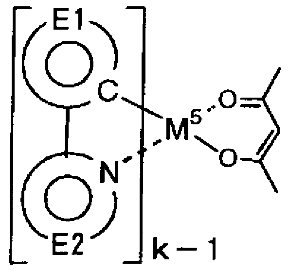
一般式 (V)中の二座配位子 L及び L'はそれぞれ以下の部分構造を有する配位子 を示す。
[化 36]
環 El及び環 El 'は各々独立に、芳香族炭化水素基又は芳香族複素環基を表し、 置換基を有していても良い。環 E2及び環 E2'は含窒素芳香族複素環基を表し、置 換基を有していても良い。 R
21、 R
22及び R
23はそれぞれハロゲン原子;アルキル基;ァ ルケニル基;アルコキシカルボ-ル基;メトキシ基;アルコキシ基;ァリールォキシ基; ジアルキルアミノ基;ジァリールァミノ基;カルバゾリル基;ァシル基;ハロアルキル基 又はシァノ基を表す。
[0119] 一般式 (V)で表される化合物として、更に好ましくは下記一般式 (Va)、 (Vb) (Vc) で表される化合物が挙げられる。
[0120] [化 37]
式中、 M
4は金属、 kは該金属の価数を表す。環 E1は置換基を有していても良い芳 香族炭化水素基を表し、環 E2は置換基を有していても良い含窒素芳香族複素環基 を表す。
[0121] [化 38]
式中、 M
5は金属、 kは該金属の価数を表す。環 E1は置換基を有していても良い芳 香族炭化水素基又は芳香族複素環基を表し、環 E2は置換基を有していても良い含 窒素芳香族複素環基を表す。
[0122] [化 39]
式中、 M6は金属、 kは該金属の価数を表し、 jは 0又は 1又は 2を表す。環 E1及び環 E1 'は各々独立に、置換基を有していても良い芳香族炭化水素基又は芳香族複素 環基を表し、環 E2及び環 E2'は各々独立に、置換基を有していても良い含窒素芳 香族複素環基を表す。
[0123] 一般式 (Va)、 (Vb)、(Vc)で表される化合物の環 El及び環 El 'として、好ましくは 、フエ-ル基、ビフヱ-ル基、ナフチル基、アントリル基、チェ-ル基、フリル基、ベン ゾチェニル基、ベンゾフリル基、ピリジル基、キノリル基、イソキノリル基、又は力ルバ ゾリル基が挙げられる。
[0124] 環 E2及び環 E2'として、好ましくは、ピリジル基、ピリミジル基、ビラジル基、トリアジ
ル基、ベンゾチアゾール基、ベンゾォキサゾール基、ベンゾイミダゾール基、キノリル 基、イソキノリル基、キノキサリル基、又はフエナントリジル基が挙げられる。
[0125] 一般式 (Va)、(Vb)及び (Vc)で表される化合物が有していても良い置換基として は、フッ素原子等のハロゲン原子;メチル基、ェチル基等の炭素数 1〜6のアルキル 基;ビュル基等の炭素数 2〜6のァルケ-ル基;メトキシカルボニル基、エトキシカル ボニル基等の炭素数 2〜6のアルコキシカルボニル基;メトキシ基、エトキシ基等の炭 素数 1〜6のアルコキシ基;フエノキシ基、ベンジルォキシ基などのァリールォキシ基; ジメチルァミノ基、ジェチルァミノ基等のジアルキルアミノ基;ジフエ-ルァミノ基等の ジァリールアミノ基;カルバゾリル基;ァセチル基等のァシル基;トリフルォロメチル基 等のハロアルキル基;シァノ基等が挙げられ、これらは互いに連結して環を形成して も良い。
[0126] なお、環 E1が有する置換基と環 E2が有する置換基が結合、又は環 E1 'が有する 置換基と環 E2'が有する置換基が結合して、一つの縮合環を形成しても良ぐこのよ うな縮合環としては 7, 8—べンゾキノリン基等が挙げられる。
[0127] 環 El、環 El '、環 E2及び環 E2'の置換基として、より好ましくはアルキル基、アル コキシ基、芳香族炭化水素基、シァノ基、ハロゲン原子、ハロアルキル基、ジァリール アミノ基、又はカルバゾリル基が挙げられる。
[0128] 式 (Va)、 (Vb)における M4な!、し M5として好ましくは、ルテニウム、ロジウム、パラジ ゥム、銀、レニウム、オスミウム、イリジウム、白金又は金が挙げられる。式 (VI)におけ る M7として好ましくは、ルテニウム、ロジウム、パラジウム、銀、レニウム、オスミウム、ィ リジゥム、白金又は金が挙げられ、特に好ましくは、白金、パラジウム等の 2価の金属 が挙げられる。
[0129] 前記一般式 (V)、 (Va)、 (Vb)及び (Vc)で示される有機金属錯体の具体例を以 下に示すが、下記の化合物に限定されるわけではない。
[0130] [化 40]
[0131] [化 41]
[0132] 前記一般式 (V)、 (Va)、 (Vb)及び (Vc)で表される有機金属錯体の中でも、特に 配位子 L及び Z又は L,として 2—ァリールピリジン系配位子(2—ァリールピリジン、こ れに任意の置換基が結合したもの、又はこれに任意の気が縮合してなるもの)を有す る化合物が好ましい。
[0133] 前記一般式 (VI)で表わされる有機金属錯体の具体例を以下に示すが、下記の化 合物に限定されるわけではない(以下において、 Meはメチル基、 Etはェチル基を示 す。)。
このような燐光性ドーパント材料の分子量は、通常 4000以下、好ましくは 3000以 下、より好ましくは 2000以下であり、また通常 200以上、好ましくは 300以上、より好 ましくは 400以上である。分子量がこの上限値を超えると、昇華性が著しく低下して 電界発光素子を制作する際に蒸着法を用いる場合において支障を来したり、或いは 有機溶媒などへの溶解性の低下や、合成工程で生じる不純物成分の増加に伴って 、材料の高純度化 (即ち劣化原因物質の除去)が困難になる場合があり、また分子 が上記下限値を下回ると、ガラス転移温度及び、融点、気化温度などが低下するた め、耐熱性が著しく損なわれるおそれがある。
[0136] これらのドーパント材料を 2種類以上使用する場合は、正孔阻止層中の正孔阻止 材料の酸ィ匕電位が、複数種のドーパント材料の中で一番大きな酸ィ匕電位を有するも のよりも大き 、ことが好ま 、。
[0137] このような有機金属錯体をドーパント材料として用いた、燐光発光を示す発光層に 使用されるホスト材料としては、本発明の有機化合物の 1種を単独で用いても良ぐ 2 種以上を混合して用いても良い。また、本発明の有機化合物と共に、蛍光発光を示 す発光層に使用されるホスト材料として前述した材料や、 4, 4' -Ν, —ジカルバ ゾールビフエ-ルなどの力ルバゾール誘導体 (WO ΟΟΖ70655号公報)、トリス(8 —ヒドロキシキノリン)ァノレミニゥム(USP 6, 303, 238号公報)、 2, 2', 2" - (1, 3 , 5—ベンゼントリル)トリス [1—フエ-ルー 1H—ベンズイミダゾール] (Appl. Phys. Lett. , 78卷, 1622頁, 2001年)、ポジビ-ルカルバゾール(特開 2001— 257076 号公報)等の 1種又は 2種以上を併用しても良い。発光層中に、本発明の有機化合 物以外のホスト材料を含む場合、その含有量は、本発明の有機化合物に対して 50 重量%以下であることが好まし 、。
[0138] 発光層中にドーパント材料として含有される有機金属錯体の量は、 0. 1重量%以 上が好ましぐまた 30重量%以下が好ましい。この下限値を下回ると素子の発光効 率向上に寄与できない場合があり、上限値を上回ると有機金属錯体同士が 2量体を 形成する等の理由で濃度消光が起き、発光効率の低下に至る可能性がある。
[0139] 燐光発光を示す発光層におけるドーパント材料の量は、従来の蛍光(1重項)を用 いた素子において、発光層に含有される蛍光性色素の量より、若干多い方が好まし い傾向がある。また、燐光性ドーパント材料と共に蛍光色素が発光層中に含有される 場合、該蛍光色素の量は、 0. 05重量%以上が好ましぐ 0. 1重量%以上がより好ま しい。また 10重量%以下が好ましぐ 3重量%以下がより好ましい。
[0140] 発光層 5の膜厚は、通常 3nm以上、好ましくは 5nm以上であり、また通常 200nm 以下、好ましくは lOOnm以下である。
[0141] 発光層 5も正孔輸送層 4と同様の方法で形成することができる。
[0142] ドーパント材料としての上述の蛍光色素及び Z又は燐光色素 (燐光性ドーパント材 料)を発光層のホスト材料としての本発明の有機化合物にドープする方法を以下に
説明する。
[0143] 塗布の場合は、本発明の有機化合物と、ドーパント材料、更に必要により、電子のト ラップや発光の消光剤とならな ヽバインダー榭脂や、レべリング剤等の塗布性改良剤 などの添加剤を添加し溶解した塗布溶液を調製し、スピンコート法などの方法により 正孔輸送層 4上に塗布し、乾燥して発光層 5を形成する。ノ インダー榭脂としては、 ポリカーボネート、ポリアリレート、ポリエステル等が挙げられる。バインダー榭脂は添 加量が多いと正孔 Z電子移動度を低下させるので、少ない方が望ましぐ発光層中 の含有量で 50重量%以下が好ま 、。
[0144] 真空蒸着法の場合には、本発明の有機化合物を真空容器内に設置されたルツボ に入れ、ドーパント材料を別のルツボに入れ、真空容器内を適当な真空ポンプで 10— 4Pa程度にまで排気した後、各々のルツボを同時に加熱して蒸発させ、ルツボと向か い合って置かれた基板上に層を形成する。また、他の方法として、上記の材料を予め 所定比で混合したものを同一のルツボを用いて蒸発させても良 、。
[0145] 上記各ドーパント材料が発光層 5中にドープされる場合、発光層の膜厚方向にお いて均一にドープされるが、膜厚方向において濃度分布があっても構わない。例え ば、正孔輸送層 4との界面近傍にのみドープしたり、逆に、正孔阻止層 6界面近傍に ドープしても良い。
[0146] 発光層 5も正孔輸送層 4と同様の方法で形成することができるが、通常は真空蒸着 法が用いられる。
なお発光層 5は、本発明の性能を損なわない範囲で上記以外の成分を含んでいて も良い。
[0147] 正孔阻止層
図 1に示す素子において、正孔阻止層 6は発光層 5の上に、発光層 5の陰極側の 界面に接するように積層される。
[0148] 正孔阻止層 6は、正孔輸送層 4から移動してくる正孔が陰極 8に到達するのを阻止 することができ、かつ、陰極 8から注入された電子を効率よく発光層 5の方向に輸送 することができる化合物より形成されることが好ましい。従って、正孔阻止層 6を構成 する材料に求められる物性としては、電子移動度が高く正孔移動度が低いことが必
要とされる。正孔阻止層 6は正孔と電子を発光層 5内に閉じこめて、発光効率を向上 させる機能を有する。
[0149] 本発明の有機電界発光素子に設けられる正孔阻止層 6のイオンィ匕ポテンシャルは 、発光層 5のイオンィ匕ポテンシャル (発光層 5がホスト材料とドーパント材料を含んで
V、る場合にはホスト材料のイオンィ匕ポテンシャル)より 0. leV以上大き 、ことが好まし
V、。イオンィ匕ポテンシャルは物質の HOMO (最高被占分子軌道)レベルにある電子 を真空準位に放出するのに必要なエネルギーで定義される。イオン化ポテンシャル は光電子分光法で直接定義されるか、電気化学的に測定した酸化電位を基準電極 に対して補正しても求められる。後者の方法の場合、例えば飽和甘コゥ電極 (SCE) を基準電極として用いたとき、下記式で定義される("Molecular Semiconductors ,,, Springer— Verlag, 1985年、 98頁)。
イオン化ポテンシャル =酸化電位 (vs. SCE) +4. 3eV
[0150] 更に、本発明の有機電界発光素子に設けられる正孔阻止層 6の電子親和力(EA) は、発光層 5の電子親和力(発光層 5がホスト材料とドーパント材料を含んでいる場合 にはホスト材料の電子親和力)と比較して同等以上であることが好ましい。電子親和 力もイオンィ匕ポテンシャルと同様に真空準位を基準として、真空準位にある電子が物 質の LUMO (最低空分子軌道)レベルに落ちて安定ィヒするエネルギーで定義される 。電子親和力は、上述のイオンィ匕ポテンシャル力 光学的バンドギャップを差し引い て求められる力 電気化学的な還元電位から下記の式で同様に求められる。
電子親和力 =還元電位 (vs. SCE) +4. 3eV
従って、本発明の有機電界発光素子に設けられる正孔阻止層 6は、酸化電位と還 元電位を用いて、
(正孔阻止材料の酸ィ匕電位) (発光層材料の酸化電位)≥0. IV
(正孔阻止材料の還元電位)≥ (発光層材料の還元電位)
と表現することちでさる。
[0151] 更に後述の電子輸送層 7を有する素子の場合には、正孔阻止層 6の電子親和力は 電子輸送層 7の電子親和力と比較して同等以下であることが好ましい。従って、 (電子輸送材料の還元電位)≥ (正孔阻止材料の還元電位)≥ (発光層材料の還元
電位)
であることが好ましい (ここで、電子輸送材料、正孔阻止材料或いは発光層材料が、 それぞれ複数用いられて ヽる場合には、最も小さ ヽ還元電位のものを比較に使用す る。また、発光層 5がホスト材料とドーパント材料を含んでいる場合には、ホスト材料の うち、最も小さい還元電位のものを比較に使用する。 ) o
[0152] このような条件を満たす正孔阻止材料として、好ましくは、下記一般式 (VII)で表さ れる混合配位子錯体が挙げられる。
[0153] [化 43]
式中、 R
1Q1〜R
1Q6は、各々独立に水素原子又は任意の置換基を表す。 M
8はアルミ ユウム、ガリウム、インジウムから選ばれる金属原子を表す。 L
5は以下に示す一般式 ( Vila) , (VIIb)、 (VIIc)のいずれかで表される。
[化 44]
-O-Ar51 ( a) O
II Κ2 ,
-O-C-Ar52 Wb)
Ar53
I
o— z: Ar54 VHc)
I
Ai
式中、 Ar51〜Ar55は、各々独立に置換基を有していても良い芳香族炭化水素基又 は置換基を有していても良い芳香族複素環基を表し、 Z3はシリコン又はゲルマニウム を表す。
[0154] 前記一般式 (VII)において、 R1Q1〜R1Q6は各々独立に水素原子又は任意の置換基 を表すが、好ましくは水素原子;塩素、臭素等のハロゲン原子;メチル基、ェチル基 等の炭素数 1〜6のアルキル基;ベンジル基等のァラルキル基;ビニル基等の炭素数 2〜6のァルケ-ル基;シァノ基;アミノ基;ァシル基;メトキシ基、エトキシ基等の炭素 数 1〜6のアルコキシ基;メトキシカルボ-ル基、エトキシカルボ-ル基等の炭素数 2 〜6のアルコキシカルボ-ル基;カルボキシル基;フエノキシ基、ベンジルォキシ基な どのァリールォキシ基;ジェチルァミノ基、ジイソプロピルアミノ基等のジアルキルアミ ノ基;ジベンジルァミノ基、ジフエネチルァミノ基などのジァラルキルアミノ基;トリフル ォロメチル基等の aーハロアルキル基;水酸基;置換基を有していても良いフエ-ル 基、ナフチル基等の芳香族炭化水素基;置換基を有していても良いチェニル基、ピリ ジル基等の芳香族複素環基を表す。
[0155] 前記芳香族炭化水素基及び芳香族複素環基が有しうる置換基としては、フッ素原 子等のハロゲン原子;メチル基、ェチル基等の炭素数 ;L〜6のアルキル基;ビニル基 等の炭素数 2〜6のァルケ-ル基;メトキシカルボ-ル基、エトキシカルボ-ル基等の 炭素数 2〜6のアルコキシカルボニル基;メトキシ基、エトキシ基等の炭素数 1〜6のァ ルコキシ基;フエノキシ基、ベンジルォキシ基などのァリールォキシ基;ジメチルァミノ 基、ジェチルァミノ基等のジアルキルアミノ基;ァセチル基等のァシル基;トリフルォロ メチル基等のハロアルキル基;シァノ基等が挙げられる。
[0156] R1Q1〜R1Q6としてより好ましくは各々独立に水素原子、アルキル基、ハロゲン原子又 はシァノ基が挙げられる。また R1Mとしては、シァノ基が特に好ましい。
[0157] 前記一般式 (Vila)、 (Vllb)、 (VIIc)中、 Ar51〜Ar55として、具体的には、各々独立 に、置換基を有していても良いフエニル基、ビフエ-ル基、ナフチル基等の芳香族炭 化水素基又はチェ-ル基、ピリジル基等の芳香族複素環基が挙げられる。
[0158] 前記一般式 (VII)で表される化合物の好ましい具体例を以下に示すが、これらに限 定するものではない。
[0160] [化 46]
[0161] なお、これらの化合物は正孔阻止層 6中に、 1種を単独で用いても良いし、必要に
応じて 2種以上を混合して用いても良 、。
[0162] 正孔阻止材料としては、前記一般式 (VII)で表される混合配位子錯体の他に、以下 の構造式で示される 1, 2, 4 トリァゾール環残基を少なくとも 1個有する化合物を用 いることちでさる。
[0163] [化 47]
[0164] 上記構造式で表される 1, 2, 4 トリァゾール環残基を少なくとも 1個有する化合物 の具体例を以下に示す力 これらに限定するものではない。
[0165] [化 48]
正孔阻止材料として、更に、以下の構造式で示されるフエナント口リン環を少なくとも 個有する化合物が挙げられる。
[0168] 上記構造式で表されるフ ナント口リン環を少なくとも 1個有する化合物の具体例を 以下に示すが、これらに限定するものではない。
[0169] [化 50]
[0170] 正孔阻止材料としてはまた、一分子内に、 2, 4, 6—位に置換基を有するピリジン 環を有する化合物を使用することが好ましい。具体例としては以下のものが挙げられ る。
[0171] [化 51]
[0172] 正孔阻止層 6の膜厚は、通常 0. 3nm以上、好ましくは 0. 5nm以上であり、また通 常 lOOnm以下、好ましくは 50nm以下である。
[0173] 正孔阻止層も 6正孔輸送層 4と同様の方法で形成することができるが、通常は真空
蒸着法が用いられる。
[0174] ただし、本発明において用いる有機化合物は、有機電界発光素子の発光層のホス ト材料として優れたものであり、後述の実施例に示すように、本発明においては、正 孔阻止層を設けなくても十分に良好な特性を得ることができる。
[0175] 陰極
陰極 8は、正孔阻止層 6を介して発光層 5に電子を注入する役割を果たす。陰極 8 として用いられる材料は、前記陽極 2に使用される材料を用いることが可能である力 効率よく電子注入を行なうには、仕事関数の低い金属が好ましぐスズ、マグネシウム 、インジウム、カルシウム、セシウム、アルミニウム、銀等の適当な金属又はそれらの合 金が用いられる。具体例としては、マグネシウム 銀合金、マグネシウム インジウム 合金、アルミニウム—リチウム合金等の低仕事関数合金電極が挙げられる。
[0176] 陰極 8の膜厚は通常、陽極 2と同様である。
低仕事関数金属力 成る陰極 8を保護する目的で、この上に更に、仕事関数が高く 大気に対して安定な金属層を積層することは素子の安定性を増す。この目的のため に、アルミニウム、銀、銅、ニッケル、クロム、金、白金等の金属が使われる。
[0177] 更に、陰極 8と発光層 5又は後述の電子輸送層 7との界面に LiF、 MgF、 Li O等
2 2 の極薄絶縁膜 (0. l〜5nm)を挿入することも、素子の効率を向上させる有効な方法 である(Appl. Phys. Lett. , 70巻, 152頁, 1997年;特開平 10— 74586号公 報; IEEE Trans. Electron. Devices, 44卷, 1245頁, 1997年)。
[0178] 電子輸送層
素子の発光効率を更に向上させることを目的として、図 2及び図 3に示すように、正 孔阻止層 6と陰極 8の間に電子輸送層 7が設けられることが好ましい。電子輸送層 7 は、電界を与えられた電極間において陰極 8から注入された電子を効率よく正孔阻 止層 6の方向に輸送することができる化合物より形成される。
[0179] このような条件を満たす材料としては、 8 ヒドロキシキノリンのアルミニウム錯体な どの金属錯体(特開昭 59— 194393号公報)、 10 ヒドロキシベンゾ [h]キノリンの金 属錯体、ォキサジァゾール誘導体、ジスチリルビフエ-ル誘導体、シロール誘導体、 3—又は 5—ヒドロキシフラボン金属錯体、ベンズォキサゾール金属錯体、ベンゾチア
ゾール金属錯体、トリスべンズイミダゾリルベンゼン(米国特許第 5, 645, 948号)、 キノキサリンィ匕合物(特開平 6— 207169号公報)、フ ナント口リン誘導体 (特開平 5 331459号公報)、 2 tーブチノレー 9, 10—N, N,ージシァノアントラキノンジイミ ン、 n型水素化非晶質炭化シリコン、 n型硫化亜鉛、 n型セレンィ匕亜鉛などが挙げられ る。
[0180] また、上述のような電子輸送材料に、アルカリ金属をドープする(特開平 10— 2701
71号公報、特開 2002— 100482号公報、特開 2002— 100478号公報などに記載
)ことにより、電子輸送性が向上するため好ましい。
[0181] このような電子輸送層 7を形成する場合、正孔阻止層 6の電子親和力は電子輸送 層 7の電子親和力と比較して同等以下であることが好ま 、。
[0182] また、発光層 5中の発光層材料、正孔阻止層 6の正孔阻止材料及び電子輸送層に 用いられる電子輸送材料の還元電位は、下記関係を満たすことが、発光領域を調整 し、駆動電圧を下げるという観点力も好ましい。
(電子輸送材料の還元電位)≥ (正孔阻止材料の還元電位)≥ (発光層材料の還元 電位)
ここで、電子輸送材料、正孔阻止材料或いは発光層材料が、それぞれ複数用いら れている場合には、最も小さい還元電位のものを比較に使用する。ただし、発光層 5 がホスト材料とドーパント材料を含んで 、る場合には、ホスト材料のうち最も還元電位 の小さいものを比較に使用する。
[0183] なお、前述の正孔阻止材料はこの電子輸送層 7に使用しても良い。その場合、前 述の正孔阻止材料を単独で使用して電子輸送層 7を形成しても良いし、複数併用し ても良い。
[0184] 電子輸送層 6の膜厚は、通常 5nm以上、好ましくは lOnm以上であり、また通常 20
Onm以下、好ましくは lOOnm以下である。
[0185] 電子輸送層 7は、正孔輸送層 4と同様にして塗布法或いは真空蒸着法により正孔 阻止層 6上に積層することにより形成されるが、通常は、真空蒸着法が用いられる。
[0186] 正孔注入層
正孔注入の効率を更に向上させ、かつ、有機層全体の陽極 2への付着力を改善さ
せる目的で、図 3に示すように、正孔輸送層 4と陽極 2との間に正孔注入層 3を挿入 することも行われている。正孔注入層 3を挿入することで、初期の素子の駆動電圧が 下がると同時に、素子を定電流で連続駆動した時の電圧上昇も抑制される効果があ る。
[0187] 正孔注入層 3に用いられる材料に要求される条件としては、陽極 2とのコンタクトが よく均一な薄膜が形成でき、熱的に安定であることが挙げられ、融点及びガラス転移 温度が高ぐ融点としては 300°C以上、ガラス転移温度としては 100°C以上であること が好ましい。更に、イオン化ポテンシャルが低く陽極 2からの正孔注入が容易なこと、 正孔移動度が大き 、ことが挙げられる。
[0188] この目的のために、正孔注入層 3の材料として、これまでにポルフィリン誘導体ゃフ タロシア-ンィ匕合物(特開昭 63- 295695号公報)、ヒドラゾンィ匕合物、アルコキシ置換 の芳香族ジァミン誘導体、 p- (9-アントリル)- Ν,Ν'-ジ- p-トリルァ-リン、ポリチェ-レン ビ-レンやポリ- ρ-フエ-レンビ-レン、ポリア-リン (Appl.Phys丄 ett.,64卷、 1245頁, 1 994年)、ポリチォフェン(OpticalMaterials,9卷、 125頁、 1998年)、スターバスト型芳香 族トリァミン (特開平 4-308688号公報)等の有機化合物や、スパッタ 'カーボン膜 (Syn th.Met.,91卷、 73頁、 1997年)や、バナジウム酸化物、ルテニウム酸化物、モリブデン 酸化物等の金属酸化物 O.Phys.D,29卷、 2750頁、 1996年)が報告されている。
[0189] また、正孔注入'輸送性の低分子有機化合物と電子受容性化合物を含有する層( 特開平 11— 251067号公報、特開 2000— 159221号公報等に記載)や、芳香族ァ ミノ基等を含有する非共役系高分子化合物に、必要に応じて電子受容性化合物をド ープしてなる層(特開平 11— 135262号公報、特開平 11— 283750号公報、特開 2 000— 36390号公報、特開 2000— 150168号公報、特開平 2001— 223084号公 報、及び W097/33193号公報など)、又はポリチォフェン等の導電性ポリマーを含 む層(特開平 10— 92584号公報)なども挙げられる力 これらに限定されるものでは ない。
[0190] 上記正孔注入層 3の材料としては、低分子 '高分子いずれの化合物を用いることも 可能である。
[0191] 低分子化合物のうち、よく使用されるものとしては、ポルフィンィ匕合物又はフタロシア
ニンィ匕合物が挙げられる。これらの化合物は中心金属を有していても良いし、無金属 のものでも良い。これらの化合物の好ましい例としては、以下の化合物が挙げられる ポノレフィン、
5,10,15,20-テトラフエニル- 21H,23H-ポルフィン、
5,10,15,20-テトラフエ-ル- 21H,23H-ポルフィンコバルト(Π)、
5,10,15,20-テトラフエ-ル- 21H,23H-ポルフィン銅(11)、
5,10,15,20-テトラフエ-ル- 21H,23H-ポルフィン亜鉛(11)、
5,10,15,20-テトラフエ-ル- 21H,23H-ポルフィンバナジウム(IV)ォキシド、
5,10,15,20-テトラ (4-ピリジル) -21H,23H-ポルフィン、
29H,31H-フタロシアニン、
銅(II)フタロシアニン、
亜鉛(II)フタロシアニン、
チタンフタロシアニンォキシド、
マグネシウムフタロシアニン、
鉛フタロシアニン、
銅(II) 4,4'4",4" '-テトラァザ- 29H,31H-フタロシアニン
[0192] 正孔注入層 3も、正孔輸送層 4と同様にして薄膜形成可能であるが、無機物の場合 には、更に、スパッタ法ゃ電子ビーム蒸着法、プラズマ CVD法が用いられる。
[0193] 以上の様にして形成される正孔注入層 3の膜厚は、低分子化合物を用いて形成さ れる場合、下限は通常 3nm、好ましくは lOnm程度であり、上限は通常 100nm、好 ましくは 50nm程度である。
[0194] 正孔注入層 3の材料として、高分子化合物を用いる場合は、例えば、前記高分子 化合物や電子受容性化合物、更に必要により正孔のトラップとならない、バインダー 榭脂ゃレべリング剤等の塗布性改良剤などの添加剤を添加し溶解した塗布溶液を 調製し、スプレー法、印刷法、スピンコート法、ディップコート法、ダイコート法などの 通常のコーティング法や、インクジェット法等により陽極 2上に塗布し、乾燥することに より正孔注入層 3を薄膜形成することができる。バインダー榭脂としては、ポリカーボ
ネート、ポリアリレート、ポリエステル等が挙げられる。バインダー榭脂は該層中の含 有量が多いと正孔移動度を低下させる虞があるので、少ない方が望ましぐ正孔注入 層 3中の含有量で 50重量%以下が好ましい。
[0195] また、フィルム、支持基板、ロール等の媒体に、前述の薄膜形成方法によって予め 薄膜を形成しておき、媒体上の薄膜を、陽極 2上に熱転写又は圧力転写すること〖こ より、薄膜形成することもできる。
[0196] 以上のようにして、高分子化合物を用いて形成される正孔注入層 3の膜厚の下限 は通常 5nm、好ましくは lOnm程度であり、上限は通常 1000nm、好ましくは 500η m程度である。
[0197] 層構成
本発明の有機電界発光素子は、図 1とは逆の構造、即ち、基板 1上に陰極 8、正孔 阻止層 6、発光層 5、正孔輸送層 4、陽極 2の順に積層することも可能であり、既述し たように少なくとも一方が透明性の高い 2枚の基板の間に本発明の有機電界発光素 子を設けることも可能である。同様に、図 2又は図 3に示した前記各層構成とは逆の 順に積層することも可能である。また、図 1〜3のいずれの層構成においても、本発明 の趣旨を逸脱しない範囲で、上述以外の任意の層を有していても良ぐまた上記複 数の層の機能を併有する層を設けることにより、層構成を簡略ィ匕する等、適宜変形を 加えることが可能である。
[0198] 或いはまた、トップェミッション構造や陰極 ·陽極共に透明電極を用いて透過型とす ること、更には、図 1に示す層構成を複数段重ねた構造 (発光ユニットを複数積層さ せた構造)とすることも可能である。その際には段間 (発光ユニット間)の界面層(陽極 が ITO、陰極が A1の場合はその 2層)の代わりに、例えば V Ο等を電荷発生層(CG
2 5
L)として用いると段間の障壁が少なくなり、発光効率'駆動電圧の観点からより好まし い。
[0199] 本発明は、有機電界発光素子が、単一の素子、アレイ状に配置された構造からな る素子、陽極と陰極力 ¾—Υマトリックス状に配置された構造の 、ずれにお!、ても適 用することができる。
実施例
[0200] 次に、本発明を実施例によって更に具体的に説明する力 本発明はその要旨を超 えない限り、以下の実施例の記載に限定されるものではな 、。
[0201] [有機化合物の合成例]
本発明の有機化合物及び本発明の電荷輸送材料として使用可能な有機化合物の 合成例を、以下の合成例に示す。なお、以下において、ガラス転移温度 (Tg)は DS C測定、気化温度は TG— DTA測定、融点は TG— DTA測定によりそれぞれ求めた
[0202] 合成例 1
(0 目的物 1の合成
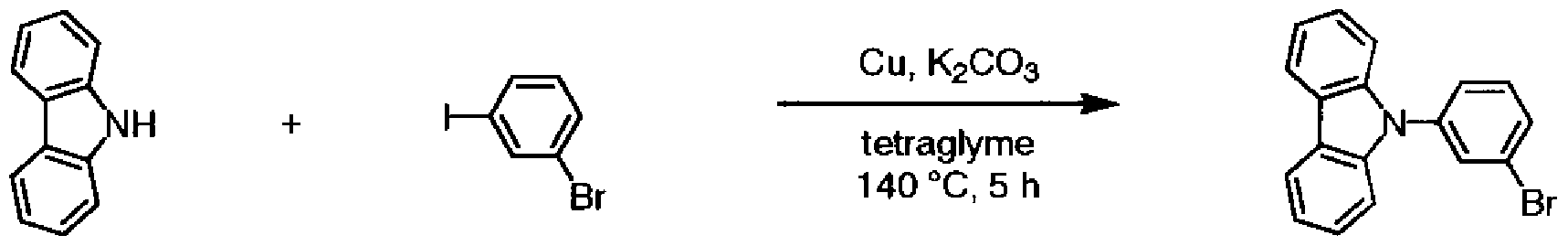
[化 52]
目的物 1 窒素気流中、力ルバゾール(7. OOg)、 3—ブロモヨードベンゼン(14. 2g)、銅粉末 (2. 66g)、炭酸カリウム(5. 79g)、及びテトラグライム(10ml)を、 140°Cに加熱下、 5時間撹拌し、室温まで放冷した。反応終了後、反応液にクロ口ホルムを加え、不溶 物を濾別した。濾液に含まれるクロ口ホルムを減圧留去し、シリカゲルカラムクロマトグ ラフィー (n キサン Zトルエン =4Zl)で精製した。減圧乾燥することにより、 目的 物 1 (10. 5g、収率 78%)を無色粘調液体として得た。
[0203] GO 目的物 2の合成
[化 53]
目的物 目的物 2
窒素気流中、 目的物 1 (10. 5g)、ビス (ピナコラートジボロン) (9. 93g)、酢酸力リウ ム(10. 9g)、及び脱水ジメチルスルホキシド(DMSO) (190ml)を、 60°Cに加熱下 、 15分間撹拌し、 [1, 1,一ビス(ジフエ-ルホスフイノ)フエ口セン]ジクロロパラジウム( Π)ジクロロメタン錯体 (0. 799g)をカ卩え、 80°Cに加熱下、 9時間撹拌した。室温まで 放冷した後、反応液に水(250ml)、及びトルエン(500ml)を加え、攪拌した。水層 をトルエンで 2回再抽出した後、有機層を合わせ、硫酸マグネシウム及び活性白土を 加えた。硫酸マグネシウム及び活性白土を濾別し、トルエンを減圧留去した。析出し た結晶を冷メタノールで洗浄し、減圧乾燥することにより、 目的物 2 (9. 86g、収率 80 %)を白色結晶として得た。
(iii) 目的物 3の合成
[化 54]
目的物 2 目的物 3 ( EM— 1 ) 窒素気流中、 6, 6,—ジブロモ— 2, 2,—ビビリジル(1. 50g)、 目的物 2 (4. 23g) 、炭酸カリウム(3. 96g)、エチレングリコールジメチルエーテル(18ml)、及び水(6m 1)を、 60°Cに加熱下、 15分間撹拌し、テトラキス(トリフエ-ルホスフィン)パラジウム( 0) (0. 277g)を加え、加熱還流下、 8時間撹拌した。室温まで放冷した後、反応液に メタノール(100ml)をカ卩え、攪拌した。析出物を濾過により回収し、メタノール Z水混 合液で洗浄した後、減圧乾燥した。得られた結晶を、シリカゲルカラムクロマトグラフィ 一 (n—へキサン Z塩化メチレン =2Zl)で精製した。更に、塩化メチレン Zメタノー ル混合液で洗浄し、減圧乾燥することにより、 目的物 3 (1. 63g、収率 53%)を白色 結晶として得た。この白色結晶 1. 51gを昇華精製したところ、白色固体 1. 41gが回 収された。
DEI -MS (m/z=638(M+))より、 目的物 3であることを確認した。
このもののガラス転移温度は 115°C、融点は 252°C、気化温度は 508°Cであった。
[0205] 合成例 2
(0 目的物 4の合成
[化 55]
目的物 4 窒素気流中、 6, 6,—ジブ口モー 2, 2,—ビビリジル(2. OOg)、 2, 5—ジフルオロフ ェ-ルボロン酸(2. 41g)、炭酸カリウム(4. 40g)、エチレングリコールジメチルエー テル(25ml)、及び水(13ml)を、 60°Cに加熱下、 15分間撹拌し、テトラキス(トリフエ -ルホスフィン)パラジウム(0) (0. 368g)を加え、加熱還流下、 6時間撹拌した。室 温まで放冷した後、反応液にメタノール(100ml)を加え、攪拌した。析出物を濾過に より回収し、メタノール Z水混合液で洗浄した後、減圧乾燥した。得られた結晶をクロ 口ホルム(150ml)に溶解させた溶液に活性白土を加え、加熱還流下、 1時間攪拌し た。濾過により不溶物を濾別し、濾液を濃縮した。析出した結晶をメタノールで洗浄し 、減圧乾燥することにより、目的物 4 (2. 16g、収率 89%)を白色結晶として得た。
[0206] (ii) 目的物 5の合成
[化 56]
目的物 4 目的物 5 ( E M— 2 ) 窒素気流中、水素化ナトリウム(55%, 1. 65g)の脱水 N, N—ジメチルホルムアミド (100ml)懸濁液に力ルバゾール(6. 33g)を添カ卩し、 80°Cに加熱下、 1時間撹拌し た後、 目的物 4 (1. 80g)を添加し、加熱還流下で 9時間撹拌した。これに氷冷下、水 (70ml)、及びメタノール(70ml)を加えて、析出した沈殿を濾別し、メタノール洗浄し 、減圧乾燥した。得られた結晶をシリカゲルカラムクロマトグラフィー(クロ口ホルム)で 精製した。更に、酢酸ェチル及びクロ口ホルム Zメタノール混合液で洗浄し、減圧乾 燥することにより、 目的物 5 (2. 15g、収率 47%)を白色結晶として得た。この白色結 晶 1. 77gを昇華精製したところ、白色固体 1. 20gが回収された。
DEI -MS (m/z=968(M+))より、 目的物 5であることを確認した。
このもののガラス転移温度は 180°C、結晶化温度は 288°C、融点は 364°C、気化 温度は 553°Cであった。
合成例 3
(0 目的物 6の合成
[化 57]
目的物 6 窒素気流中、 2, 5—ジブロモピリジン(3. OOg)、ビス(トリブチルチン)(3. 54ml)、
及び脱水キシレン(100ml)を、 60°Cに加熱下、 15分間撹拌し、テトラキス(トリフエ- ルホスフィン)パラジウム (0) (0. 35 lg)をカ卩え、加熱還流下、 8時間撹拌した。室温 まで放冷した後、反応液にクロ口ホルム(100ml)を加え、攪拌した後、不溶物を濾別 し、濾液に含まれるキシレン及びクロ口ホルムを減圧留去した。得られた残渣をシリカ ゲルカラムクロマトグラフィー (塩化メチレン/へキサン = 1/5 1/1)で精製し、メ タノールで洗浄後、減圧乾燥することにより、 目的物 6 (0. 51g、収率 25%)を白色結 晶として得た。
[0208] GO 目的物 7の合成
[化 58]
目的物 6 目的物 7 ( E M— 3 ) 窒素気流中、 目的物 6 (0. 48g)、力ルバゾール(1. 02g)、銅粉末 (0. 29g)、炭酸 カリウム(1. 06g)、及びテトラグライム (4ml)を、 200°Cに加熱下、 8時間撹拌し、室 温まで放冷した。反応終了後、反応液にクロ口ホルム(200ml)をカ卩え、不溶物を濾 別した。濾液に含まれるクロ口ホルムを減圧留去し、シリカゲルカラムクロマトグラフィ 一(n キサン Z塩化メチレン = 1/1)で精製した。酢酸ェチル及びメタノールで 洗浄後、減圧乾燥することにより、 目的物 6 (0. 42g、収率 57%)を薄黄色結晶として 得た。この薄黄色結晶 0. 42gを昇華精製したところ、薄黄色固体 0. 22gが回収され た。
DEI -MS (m/z=486(M+))より、 目的物 7であることを確認した。
このものの融点は 323°C、気化温度は 443°Cであった。
[0209] 合成例 4
(0 目的物 8の合成
0 °C→rt, 7.5h
目的物 8 窒素気流中、 2, 5—ジブロモピリジン(19. 5g)、テトラキス(トリフエ-ルホスフィン) パラジウム(0) (4. 33g)、及びテトラヒドロフラン (THF) (75ml)の混合物を 0°Cに冷 却し、 2—ピリジルジンタブロマイドの 0. 5Mの THF溶液(150ml)を滴下した後、室 温まで昇温し、 7. 5時間攪拌した。反応混合物に、水 (400ml)にエチレンジァミン四 酢酸 (EDTA) (20g)、及び炭酸ナトリウム(20g)を溶解させた水溶液をカ卩えた後、ク ロロホルム(300ml)で 2回抽出した。有機層を硫酸マグネシウムで乾燥、濃縮した後 、カラムクロマトグラフィー (塩化メチレン Z酢酸ェチル = 1Z0〜20Z1)で精製する ことにより、 目的物 8 (7. 27g、収率 41%)を得た。
GO 目的物 9の合成
[化 60]
目的物 8 目的物 9 窒素気流中、 目的物 8 (4—ブロモー 2, 2,—ビビリジル) (2. 40g)、 2, 5—ジフル オロフェ-ルボロン酸(2. 94g)、炭酸カリウム(4. 23g)、エチレングリコールジメチル エーテル(20ml)、及び水(10ml)を、 60°Cに加熱下、 15分間撹拌し、テトラキス(ト リフエ-ルホスフィン)パラジウム(0) (0. 294g)を加え、加熱還流下、 8時間撹拌した 。室温まで放冷した後、反応液に水(150ml)をカ卩え、析出物を濾過により回収し、メ タノール Z水混合液で洗浄した後、減圧乾燥した。得られた結晶をトルエン(150ml )に溶解させた溶液に活性白土を加え、加熱還流下、 1時間攪拌した。濾過により不 溶物を濾別し、濾液を濃縮した。析出した結晶を冷エタノールで洗浄し、減圧乾燥す ることにより、 目的物 9 (0. 79g、収率 29%)を白色結晶として得た。
[0211] (iii) 目的物 10の合成
[化 61]
目的物 9 目的物 1 0
窒素気流中、水素化ナトリウム(55%, 0. 723g)の脱水 N, N—ジメチルホルムアミ ド(30ml)懸濁液に力ルバゾール(2. 77g)を添カ卩し、 80°Cに加熱下、 30分撹拌した 後、 目的物 9 (4— (2, 5—ジフルオロフェ-ル)—2, 2,—ビビリジル)(2. 40g)を添 加し、加熱還流下で 9時間撹拌した。これに氷冷下、水(70ml)、及びメタノール(70 ml)を加えて、析出した沈殿を濾別し、メタノール洗浄し、減圧乾燥した。得られた結 晶をシリカゲルカラムクロマトグラフィー(クロ口ホルム/アセトン = 1/0〜20/1)で 精製した。さらに、エタノールで洗浄し、減圧乾燥することにより、 目的物 5 (0. 322g 、収率 19%)を白色結晶として得た。
DEI -MS (m/z=562(M+))より、 目的物 10であることを確認した。
[0212] 合成例 5
(0 目的物 11の合成
[化 62]
目的物 1 1
ベンズアルデヒド(10. 6g)、ジァセチル(4. 3g)、及びピぺリジン(0. 5ml)をエタノ ール (50ml)に溶解し、加熱還流下、 2. 5時間攪拌した。放冷、冷蔵庫で冷却後、 得られた結晶を濾取した。これをメタノールで洗浄後、乾燥し、 目的物 11 (1. 39g)を
(ii) 目的物 12の合成
[化 63]
目的物 1 1 目的物 1 2
4ーブロモーフエナシルピリジ-ゥムブロミド(3. 56g)、 目的物 11 (1. 3g)、酢酸ァ ンモ -ゥム(9. 7g)、及びエタノール(100ml)を、加熱還流下、 4時間攪拌した。放 冷後、得られた結晶を濾別しメタノール(100ml)で洗浄した。乾燥後、 目的物 12 (0 . 98g)を得た。
(iii) 目的物 13の合成
[化 64]
目的物 1 2 目的物 1 3 目的物 12 (0. 90g)、力ルバゾール(0. 53g)、及びナトリウム— tert—ブトキシド(0 . 56g)にトルエン(30ml)を添加し攪拌した。これに、トリス (ジベンジリデンアセトン) ジパラジウム(0)クロ口ホルム(0. 05g)をトルエン(8ml)に溶解し、トリ— tert—ブチ ルホスフィン (0. 055g)を加えた溶液を添加し、加熱還流下、 4時間反応させた。放 冷後、得られた結晶を濾取し、メタノールで熱懸洗し、メタノール Z水混合溶媒で熱 懸洗した。さらに、カラムクロマトグラフィーによって精製し、 目的物 13 (0. 65g)を得
た。
DEI -MS (m/z=791(M+))から目的物 13であることを確認した。
このものの融点は 395°C、気化温度は 555°C、ガラス転移温度は 161°Cであった。
[0215] 合成例 6
(0 目的物 14の合成
[化 65]
目的物 1 4
3—ブロモベンズアルデヒド(30. Og)、ジァセチル(6. 98g)、及びピぺリジン(0. 8 Oml)をエタノール (80ml)に溶解し、加熱還流下、 2. 5時間攪拌した。放冷後、冷蔵 庫で冷却し、得られた結晶を濾取、メタノールで洗浄、乾燥し、目的物 14 (2. 33g)を 得た。
GO 目的物 15の合成
[化 66]
目的物 1 4 目的物 1 5 フエナシルピリジ-ゥムブロミド(2. 56g)、 目的物 14 (2. 00g)、酢酸アンモ-ゥム( 9. 30g)、及びエタノール(100ml)を、加熱還流下、 8時間攪拌した。放冷後、得ら れた結晶を濾取、メタノール(100ml)で洗浄後、乾燥し、目的物 15 (1. 30g)を得た
[0217] (iii) 目的物 16の合成
目的物 1 5 目的物 1 6 ( E M— 4 ) 目的物 15 (1. 2g)、力ルバゾール(0. 71g)、及びナトリウム— tert—ブトキシド(0. 74g)にトルエン (40ml)を添加し攪拌した。これに、トリス (ジベンジリデンアセトン)ジ パラジウム(0)クロ口ホルム(0. 066g)をトルエン(8ml)に溶解し、トリ一 tert—ブチ ルホスフィン (0. 05 lg)を加えた溶液を添加し、加熱還流 7時間攪拌した。放冷後、 得られた結晶を濾取し、メタノールで熱懸洗し、クロ口ホルムで熱懸洗を数回繰り返し 、昇華精製を行うことにより目的物 16 (0. 91g)を得た。
DEI -MS (m/z=791(M+))から目的物 16であることを確認した。
このものの融点は 316°C、気化温度は 346°C、ガラス転移温度は 140°Cであった。
[0218] 合成例 7
(0 目的物 17の合成
[化 68]
目的物 1 1 目的物 1 7
3—ブロモフエナシルピリジ-ゥムブロミド(8. 23g)、合成例 5で得られた目的物 11 (3. OOg)、酢酸アンモ -ゥム(22. 5g)、及びエタノール(200ml)を、加熱還流下、 8時間攪拌した。放冷後、得られた結晶を濾取、メタノールで加熱懸洗、乾燥後、 目 的物 17 (1. 05g)を得た。
[0219] (ii) 目的物 18の合成
目的物 1 7 目的物 1 8 目的物 17 (1. 4g)、力ルバゾール(0. 94g)、及びナトリウム— tert—ブトキシド(0. 86g)にトルエン(70ml)を添カ卩し攪拌した。これに、トリス(ジベンジリデンアセトン)ジ パラジウム(0)クロ口ホルム(0. 087g)をトルエン(8ml)に溶解し、トリ一 tert—ブチ ルホスフィン (0. 068g)を加えた溶液を添加し、加熱還流下、 7時間攪拌した。放冷 後、得られた結晶を濾別し、メタノールで熱懸洗、クロ口ホルム熱懸洗を数回繰り返し 、昇華精製を行うことにより目的物 18 (0. 70g)を得た。
DEI -MS (m/z=791(M+))から目的物 18であることを確認した。
このものの融点は 317°C、気化温度は 540°C、ガラス転移温度は 139°Cであった。
[0220] 合成例 8
(0 目的物 19の合成
[化 70]
目的物 1 9
窒素気流中、力ルバゾール(6. 82g)、4ーブロモヨードベンゼン(15. Og)、銅粉末 (2. 61g)、炭酸カリウム(11. 3g)、及びテトラグライム(30ml)を、 145°Cに加熱下、 5時間撹拌し、室温まで放冷した。反応混合物にクロ口ホルムを加え、不溶物を濾別 した。濾液に含まれるクロ口ホルムを減圧留去し、シリカゲルカラムクロマトグラフィー( n—へキサン Zトルエン =4Zl)で精製した。減圧乾燥することにより、 目的物 19 (9 . 08g、収率 69%)を白色結晶として得た。
[0221] (ii) 目的物 20の合成
[化 71]
目的物 1 9 目的物 2 0 窒素気流中、 目的物 19 (4. 50g)、ビス (ピナコラートジボロン)(4. 61g)、酢酸カリ ゥム(4. 61g)、及び DMSO (75ml)を、 60°Cにカロ熱下、 15分間撹拌し、 [1, 1,一ビ ス(ジフエ-ルホスフイノ)フエ口セン]ジクロロパラジウム(Π)ジクロロメタン錯体 (0. 34 3g)を加え、 80°Cに加熱下、 6時間撹拌した。室温まで放冷した後、反応液に水(25 Oml)、及びトルエン(500ml)をカ卩え、攪拌した。水層をトルエンで 2回再抽出した後 、有機層を合わせ、硫酸マグネシウム及び活性白土を加えた。硫酸マグネシウム及 び活性白土を濾別し、トルエンを減圧留去した。析出した結晶を冷メタノールで洗浄 し、減圧乾燥することにより、 目的物 20(4. 46g、収率 86%)を白色結晶として得た。
(iii) 目的物 21の合成
[化 72]
目的物 1 7 目的物 2 0 目的物 2 K E M- 5 ) 合成例 7で得られた目的物 17 (1. 20g)、 目的物 20 (1. 64g)、及び炭酸カリウム( 1. 07g)に、エチレングリコールジメチルエーテル(80ml)、及び水(16ml)を添加し 攪拌した。これに、テトラキス(トリフエ-ルフォスフィン)パラジウム (0) (0. l lg)を添
加し、加熱還流下、 6時間攪拌した。放冷後、濃縮した後、メタノールを添加し、析出 物を各種溶媒で洗浄した後、カラムクロマトグラフィーで精製し、 目的物 21 (1. 40g) を得た。
DEI -MS (m/z=942(M+))から目的物 21であることを確認した。
このものの融点は 369°C、気化温度は 574°C、ガラス転移温度は 155°Cであった。 合成例 9
(0 目的物 22の合成
[化 73]
目的物 2 2
2—ァセチルビリジン(9. 80g)、ベンズアルデヒド(8. 57g)、及びピぺリジン(0. 5 ml)をエタノール(20ml)に溶解し、加熱還流下、 8時間攪拌した。放冷した後、溶媒 を減圧留去し、液体状態として目的物 22 (17. Og)を得た。
GO 目的物 23の合成
[化 74]
目的物 2 2 目的物 2 3
4—ブロモフエナシルピリジ-ゥムブロミド(7. 14g)、 目的物 22 (8. 36g)、酢酸アン モ -ゥム(39. Og)、及びエタノール(200ml)を、加熱還流下、 8時間攪拌して得られ た溶液に、メタノール(50ml)添加して攪拌し、その後析出した沈殿物を濾過した。得 られた結晶をメタノール(200ml)で洗浄した。これを濾過して得られた結晶を乾燥し
目的物 2 3 目的物 2 4 目的物 23 (3. OOg)、及び 2, 5—ジフルオロフェ-ルボロン酸(1. 72g)をエチレン グリコールジメチルエーテル(70ml)に溶解し、炭酸カリウム 3. 22gを水 10ml〖こ溶解 した水溶液を脱気した後、系内に添加、系内全体を脱気、窒素置換し、加熱攪拌し た。これに、内温 60°Cで、テトラキス(トリフエ-ルフォスフィン)パラジウム(0) (0. 36g )を添加後、加熱還流下、 4時間攪拌した。放冷後、濃縮し、メタノールで懸洗した後 、メタノールにて再結晶後、乾燥して目的物 24 (2. 42g)を得た。
(iv) 目的物 25の合成
[化 76]
目的物 2 4 目的物 2 5 ( E M— 6 ) 水素化ナトリウム 55% (0. 62g)を脱水ジメチルホルムアミド 50mlに懸濁攪拌し、力 ルバゾール(2. 38g)を少しづつ系内に添カ卩した。添カ卩終了後、 80°Cまで昇温し、 目
的物 24 (1. 5g)を添加した。加熱還流下、 12時間攪拌し、放冷後、メタノール(200 ml)、及び水 (40ml)に注いだ。得られた結晶を濾取し、メタノールで熱懸洗した後、 塩化メチレン Zメタノールで再結晶後、カラムクロマトグラフィーで精製し、 目的物 25 ( 0. 81g)を得た。
DEI -MS (m/z=714(M+))から目的物 25であることを確認した。
このものの融点は 282°C、気化温度は 508°C、ガラス転移温度は 152°Cであった。
[0227] [有機電界発光素子の作製例]
以下に、本発明の有機電界発光素子の作製例を示す。
なお、以下において、作製した有機電界発光素子の一部については、下記の駆動 寿命試験を行った。
[0228] 〈駆動寿命試験〉
温度:室温
駆動方式:直流駆動 (DC駆動)
初期輝度: 2, 500cd/m2
定電流で連続発光させ、駆動開始から 1,000時間後の輝度及び電圧上昇を比較し た。それぞれ、初期輝度 (L )に対する 1,000時間後の輝度 (L )の割合 (L ZL
0 1,000 1,000 0
)、及び、初期電圧 (V )から 1,000時間後の電圧 (V )の上昇値(
0 1,000 Δν=ν -V )
1,000 0 を求めた。
[0229] 実施例 1
図 3に示す構造を有する有機電界発光素子を以下の方法で作製した。
ガラス基板 1の上にインジウム'スズ酸ィ匕物 (ΙΤΟ)透明導電膜を 150應堆積したも の (スパッター成膜品;シート抵抗 15 Ω )を通常のフォトリソグラフィ技術と塩酸エッチ ングを用いて 2mm幅のストライプにパターニングして陽極 2を形成した。パターン形成 した ITO基板を、アセトンによる超音波洗浄、純水による水洗、イソプロピルアルコー ルによる超音波洗浄の順で洗浄後、窒素ブローで乾燥させ、最後に紫外線オゾン洗 浄を行った。
[0230] 正孔注入層 3の材料として、下記に示す構造式の芳香族アミノ基を有する非共役 系高分子化合物(PB— 1 (重量平均分子量: 29400,数平均分子量: 12600) )を下記
に示す構造式の電子受容性ィ匕合物 (A— 2)と共に以下の条件でスピンコートした。
[0231] [化 77]
[0233] スピンコート条件
溶媒 安息香酸ェチル
塗布液濃度 2[wt%]
ΡΒ-1:Α-2 10 :2 (重量比)
スピナ回転数 1500[rpm]
スピナ回転時間 30 [秒]
乾燥条件 230[°C]X15 [分]
[0234] 上記のスピンコートにより膜厚 30應の均一な薄膜が形成された。
[0235] 次に、正孔注入層 3を成膜した基板を真空蒸着装置内に設置した。上記装置の粗
排気を油回転ポンプにより行った後、装置内の真空度が 5.2 X 10— 5Pa (約 3.9 X 10— 7To rr)以下になるまでクライオポンプを用いて排気した。上記装置内に配置されたセラミ ックるつぼに入れた、下記に示すァリールアミンィ匕合物 (H— 1)をるつぼの周囲のタ ンタル線ヒーターで加熱して蒸着を行った。この時のるつぼの温度は、 258〜271°Cの 範囲で制御した。蒸着時の真空度 5.8 X 10— 5Pa (約 4.4 X 10— 7Torr)、蒸着速度は 0.18η m/秒で膜厚 40nmの正孔輸送層 4を得た。
[化 79]
引続き、発光層 5の主成分 (ホスト材料)として合成例 1で合成された目的物 3 (以下 の EM— 1)を、副成分 (ドーパント)として有機イリジウム錯体 (D- 1)を別々のセラミ ックるつぼに設置し、 2元同時蒸着法により成膜を行った。
[化 80]
[0237] 目的物 3 (EM— 1)のるつぼ温度は 307〜309°C、蒸着速度は O.lOnmZ秒に、化合 物(D— 1)のるつぼ温度は 244〜245°Cにそれぞれ制御し、膜厚 30nmで化合物(D— 1)が約 6重量%含有された発光層 5を正孔輸送層 4の上に積層した。蒸着時の真空 度は 5.5 X 10—
5Pa (約 4.1 X 10—
7Torr)であった。
[0238] 更に、正孔阻止層 6として下記に示すピリジン誘導体 (HB— 1)をるつぼ温度を 213 〜216°Cとして、蒸着速度 0.08應/秒で 5應の膜厚で積層した。蒸着時の真空度は 4. 9 X 10— (約3.7 10— 7Torr)であった。
[0239] [化 81]
[0240] 次に、正孔阻止層 6の上に、電子輸送層 7として下記に示すアルミニウムの 8—ヒド 口キシキノリン錯体 (ET— 1)を同様にして蒸着した。この時のアルミニウムの 8—ヒドロ キシキノリン錯体のるつぼ温度は 250〜260°Cの範囲で制御し、蒸着時の真空度は 5. 0 X 10— 5Pa (約 3.8 X 10— 7Torr)、蒸着速度は 0.21nm/秒で膜厚は 30nmとした。
[0241] [化 82]
上記の正孔注入層 3、正孔輸送層 4、発光層 5、正孔阻止層 6及び電子輸送層 7を 真空蒸着する時の基板温度は室温に保持した。
[0243] ここで、電子輸送層 6までの蒸着を行った素子を一度前記真空蒸着装置内より大 気中に取り出して、陰極蒸着用のマスクとして 2mm幅のストライプ状シャドーマスクを、 陽極 2の ITOストライプとは直交するように素子に密着させて、別の真空蒸着装置内 に設置して有機層と同様にして装置内の真空度が 2.0 X 10"
6Torr (約 2.7 X 10"
4Pa)以 下になるまで排気した。陰極 8として、先ず、フッ化リチウム (LiF)をモリブデンボートを 用いて、蒸着速度 0.03nm/秒、真空度 2.8 X 10—
6Torr (約 3.7 X 10—
4Pa)で、 0.5nmの膜 厚で電子輸送層 7の上に成膜した。次に、アルミニウムを同様にモリブデンボートによ り加熱して、蒸着速度 0.46nm/秒、真空度 9.6 X 10—
6Torr (約 1.3 X 10"
3Pa)で膜厚 80nm のアルミニウム層を形成して陰極 8を完成させた。以上の 2層型陰極 8の蒸着時の基 板温度は室温に保持した。
[0244] 以上の様にして、 2mm X 2mmのサイズの発光面積部分を有する有機電界発光素子 が得られた。
この素子の発光特性及び寿命特性を表 1に示す。
素子の発光スペクトルの極大波長は 512nm、色度は CIE(x,y)=(0.30,0.60)であり、有 機イリジウム錯体 (D— 1)力ものものと同定された。
この素子は、後述の比較例の素子と比較して発光効率が高ぐ長寿命であった。
[0245] 実施例 2
正孔阻止層のピリジン誘導体 (HB— 1)を積層しなカゝつた他は実施例 1と同様にし て素子を作製した。
この素子の発光特性及び寿命特性を表 1に示す。
素子の発光スペクトルの極大波長は 512nm、色度は CIE(x,y)=(0.29,0.60)であり、有 機イリジウム錯体 (D— 1)力ものものと同定された。
この素子では、正孔阻止層なしでも有機イリジウム錯体力ゝらの発光が高効率で得ら れた。
[0246] 実施例 3
発光層 5の主成分 (ホスト材料)として目的物 3 (EM- 1)の代わりに下記に示す目 的物 5 (以下の EM— 2)を用いた他は実施例 1と同様にして素子を作製した。
この素子の発光特性を表 1に示す。
素子の発光スペクトルの極大波長は 514nm、色度は CIE(x,y)=(0.30,0.61)であり、有 機イリジウム錯体 (D— 1)力ものものと同定された。
この素子では、有機イリジウム錯体力ゝらの発光が高効率で得られ、駆動電圧も低か つ 7こ。
[化 83]
[0247] 実施例 4
正孔阻止層のピリジン誘導体 (HB— 1)を積層しなカゝつた他は実施例 3と同様にし て素子を作製した。
この素子の発光特性を表 1に示す。
素子の発光スペクトルの極大波長は 514nm、色度は CIE(x,y)=(0.30,0.61)であり、有 機イリジウム錯体 (D— 1)力ものものと同定された。
この素子では、正孔阻止層なしでも有機イリジウム錯体力ゝらの発光が高効率で得ら れ、駆動電圧も低かった。
[0248] 実施例 5
発光層 5の主成分 (ホスト材料)として目的物 3 (EM- 1)の代わりに下記に示す目 的物 7 (以下の EM— 3)を用いた他は実施例 1と同様にして素子を作製した。
この素子の発光特性を表 1に示す。
素子の発光スペクトルの極大波長は 513nm、色度は CIE(x,y)=(0.30,0.61)であり、有 機イリジウム錯体 (D— 1)力ものものと同定された。
[0249] 実施例 6
正孔阻止層のピリジン誘導体 (HB— 1)を積層しなカゝつた他は実施例 5と同様にし て素子を作製した。
この素子の発光特性を表 1に示す。
素子の発光スペクトルの極大波長は 513nm、色度は CIE(x,y)=(0.30,0.61)であり、有 機イリジウム錯体 (D— 1)力ものものと同定された。
この素子では、正孔阻止層なしでも有機イリジウム錯体力ゝらの発光が高効率で得ら れ、比較例 1および比較例 2と比較して、駆動電圧も低かった。
[0250] 実施例 7
発光層 5の主成分 (ホスト材料)として目的物 3 (EM- 1)の代わりに下記に示す目 的物 16 (EM— 4)を用いた他は実施例 2と同様にして素子を作製した。
この素子の発光特性を表 1に示す。
素子の発光スペクトルの極大波長は 513nm、色度は CIE(x,y)=(0.30,0.61)であり、有 機イリジウム錯体 (D— 1)力ものものと同定された。
この素子では、正孔阻止層なしで有機イリジウム錯体力ゝらの発光が高効率で得られ 、比較例 2と比較して、電圧も低力つた。
[化 85]
実施例 8
発光層 5の主成分 (ホスト材料)として目的物 3 (EM- 1)の代わりに下記に示す目 的物 21 (EM— 5)を用いた他は実施例 2と同様にして素子を作製した。
この素子の発光特性を表 1に示す。
素子の発光スペクトルの極大波長は 513nm、色度は CIE(x,y)=(0.30,0.61)であり、有 機イリジウム錯体 (D— 1)力ものものと同定された。
この素子では、正孔阻止層なしで有機イリジウム錯体力ゝらの発光が高効率で得られ 、比較例 2と比較して、電圧も低力つた。
[化 86]
実施例 9
発光層 5の主成分 (ホスト材料)として目的物 3 (EM- 1)の代わりに下記に示す目 的物 25 (EM— 6)を用いた他は実施例 1と同様にして素子を作製した。
この素子の発光特性を表 1に示す。
素子の発光スペクトルの極大波長は 514nm、色度は CIE(x,y)=(0.31,0.61)であり、有 機イリジウム錯体 (D— 1)力ものものと同定された。
この素子では、有機イリジウム錯体力もの発光が高効率で得られ、比較例 1と比較し て、電圧も低かった。
[化 87]
[0253] 実施例 10
正孔阻止層のピリジン誘導体 (HB— 1)を積層しなカゝつた他は実施例 9と同様にし て素子を作製した。
この素子の発光特性を表 1に示す。
素子の発光スペクトルの極大波長は 515nm、色度は CIE(x,y)=(0.31,0.62)であり、有 機イリジウム錯体 (D— 1)力ものものと同定された。
この素子では、正孔阻止層なしでも有機イリジウム錯体力ゝらの発光が高効率で得ら れ、比較例 2と比較して、電圧も低力 た。
[0254] 比較例 1
発光層 5の主成分 (ホスト材料)として目的物 (EM— 1)の代わりに下記に示す (CB
P)を用いた他は実施例 1と同様にして素子を作製した。
この素子の発光特性及び寿命特性を表 1に示す。
素子の発光スペクトルの極大波長は 514nm、色度は CIE(x,y)=(0.30,0.58)であり、有 機イリジウム錯体 (D— 1)力ものものと同定された。
この素子は、実施例 1〜6の素子と比較して発光効率が低力つた。
[化 88]
[0255] 比較例 2
正孔阻止層のピリジン誘導体 (HB— 1)を積層しなカゝつた他は比較例 1と同様にし て素子を作製した。
この素子の発光特性を表 1に示す。
素子の発光スペクトルの極大波長は 512nm、色度は CIE(x,y)=(0.30,0.60)であり、有 機イリジウム錯体 (D— 1)力ものものと同定された。
この素子では、正孔阻止層なしでも有機イリジウム錯体からの発光が得られたが、 実施例 1〜6の素子と比較して、発光効率が低力つた。また、実施例 1及び 2の素子と 比較して、駆動電圧も高カゝつた。
[0256] [表 1]
以上の通り、実施例 1 4の素子は、比較例 1, 2の素子と比較して発光効率が高く 、また、特に実施例 1、実施例 2の素子は比較例 1の素子と比較して輝度が高ぐか
つ、電圧上昇が小さい。これらの結果から、本発明の有機化合物を用いることにより、 高効率で、駆動安定性に優れた長寿命な燐光素子が実現されることが明らかである 本発明を特定の態様を用いて詳細に説明したが、本発明の意図と範囲を離れるこ となく様々な変更が可能であることは当業者に明らかである。
なお、本出願は、 2005年 1月 25日付で出願された日本特許出願 (特願 2005— 1 7098)に基づいており、その全体が引用により援用される。