WO2006105247A2 - Bridgeless boost converter with pfc circuit - Google Patents

Bridgeless boost converter with pfc circuit Download PDF

Info

Publication number
WO2006105247A2
WO2006105247A2 PCT/US2006/011556 US2006011556W WO2006105247A2 WO 2006105247 A2 WO2006105247 A2 WO 2006105247A2 US 2006011556 W US2006011556 W US 2006011556W WO 2006105247 A2 WO2006105247 A2 WO 2006105247A2
Authority
WO
WIPO (PCT)
Prior art keywords
switches
voltage
input
circuit
boost converter
Prior art date
Legal status (The legal status is an assumption and is not a legal conclusion. Google has not performed a legal analysis and makes no representation as to the accuracy of the status listed.)
Ceased
Application number
PCT/US2006/011556
Other languages
French (fr)
Other versions
WO2006105247B1 (en
WO2006105247A3 (en
Inventor
Peter Wood
Current Assignee (The listed assignees may be inaccurate. Google has not performed a legal analysis and makes no representation or warranty as to the accuracy of the list.)
Infineon Technologies Americas Corp
Original Assignee
International Rectifier Corp USA
Priority date (The priority date is an assumption and is not a legal conclusion. Google has not performed a legal analysis and makes no representation as to the accuracy of the date listed.)
Filing date
Publication date
Application filed by International Rectifier Corp USA filed Critical International Rectifier Corp USA
Priority to JP2008504329A priority Critical patent/JP2008535460A/en
Priority to EP06739998A priority patent/EP1864372A2/en
Publication of WO2006105247A2 publication Critical patent/WO2006105247A2/en
Publication of WO2006105247A3 publication Critical patent/WO2006105247A3/en
Publication of WO2006105247B1 publication Critical patent/WO2006105247B1/en
Anticipated expiration legal-status Critical
Ceased legal-status Critical Current

Links

Classifications

    • HELECTRICITY
    • H02GENERATION; CONVERSION OR DISTRIBUTION OF ELECTRIC POWER
    • H02MAPPARATUS FOR CONVERSION BETWEEN AC AND AC, BETWEEN AC AND DC, OR BETWEEN DC AND DC, AND FOR USE WITH MAINS OR SIMILAR POWER SUPPLY SYSTEMS; CONVERSION OF DC OR AC INPUT POWER INTO SURGE OUTPUT POWER; CONTROL OR REGULATION THEREOF
    • H02M3/00Conversion of DC power input into DC power output
    • H02M3/02Conversion of DC power input into DC power output without intermediate conversion into AC
    • H02M3/04Conversion of DC power input into DC power output without intermediate conversion into AC by static converters
    • H02M3/10Conversion of DC power input into DC power output without intermediate conversion into AC by static converters using discharge tubes with control electrode or semiconductor devices with control electrode
    • H02M3/145Conversion of DC power input into DC power output without intermediate conversion into AC by static converters using discharge tubes with control electrode or semiconductor devices with control electrode using devices of a triode or transistor type requiring continuous application of a control signal
    • H02M3/155Conversion of DC power input into DC power output without intermediate conversion into AC by static converters using discharge tubes with control electrode or semiconductor devices with control electrode using devices of a triode or transistor type requiring continuous application of a control signal using semiconductor devices only
    • HELECTRICITY
    • H02GENERATION; CONVERSION OR DISTRIBUTION OF ELECTRIC POWER
    • H02MAPPARATUS FOR CONVERSION BETWEEN AC AND AC, BETWEEN AC AND DC, OR BETWEEN DC AND DC, AND FOR USE WITH MAINS OR SIMILAR POWER SUPPLY SYSTEMS; CONVERSION OF DC OR AC INPUT POWER INTO SURGE OUTPUT POWER; CONTROL OR REGULATION THEREOF
    • H02M1/00Details of apparatus for conversion
    • H02M1/0083Converters characterised by their input or output configuration
    • H02M1/0085Partially controlled bridges
    • HELECTRICITY
    • H02GENERATION; CONVERSION OR DISTRIBUTION OF ELECTRIC POWER
    • H02MAPPARATUS FOR CONVERSION BETWEEN AC AND AC, BETWEEN AC AND DC, OR BETWEEN DC AND DC, AND FOR USE WITH MAINS OR SIMILAR POWER SUPPLY SYSTEMS; CONVERSION OF DC OR AC INPUT POWER INTO SURGE OUTPUT POWER; CONTROL OR REGULATION THEREOF
    • H02M1/00Details of apparatus for conversion
    • H02M1/42Circuits or arrangements for compensating for or adjusting power factor in converters or inverters
    • H02M1/4208Arrangements for improving power factor of AC input
    • H02M1/4233Arrangements for improving power factor of AC input using a bridge converter comprising active switches
    • HELECTRICITY
    • H02GENERATION; CONVERSION OR DISTRIBUTION OF ELECTRIC POWER
    • H02MAPPARATUS FOR CONVERSION BETWEEN AC AND AC, BETWEEN AC AND DC, OR BETWEEN DC AND DC, AND FOR USE WITH MAINS OR SIMILAR POWER SUPPLY SYSTEMS; CONVERSION OF DC OR AC INPUT POWER INTO SURGE OUTPUT POWER; CONTROL OR REGULATION THEREOF
    • H02M7/00Conversion of AC power input into DC power output; Conversion of DC power input into AC power output
    • H02M7/02Conversion of AC power input into DC power output without possibility of reversal
    • H02M7/04Conversion of AC power input into DC power output without possibility of reversal by static converters
    • H02M7/12Conversion of AC power input into DC power output without possibility of reversal by static converters using discharge tubes with control electrode or semiconductor devices with control electrode
    • H02M7/21Conversion of AC power input into DC power output without possibility of reversal by static converters using discharge tubes with control electrode or semiconductor devices with control electrode using devices of a triode or transistor type requiring continuous application of a control signal
    • H02M7/217Conversion of AC power input into DC power output without possibility of reversal by static converters using discharge tubes with control electrode or semiconductor devices with control electrode using devices of a triode or transistor type requiring continuous application of a control signal using semiconductor devices only
    • H02M7/219Conversion of AC power input into DC power output without possibility of reversal by static converters using discharge tubes with control electrode or semiconductor devices with control electrode using devices of a triode or transistor type requiring continuous application of a control signal using semiconductor devices only in a bridge configuration
    • YGENERAL TAGGING OF NEW TECHNOLOGICAL DEVELOPMENTS; GENERAL TAGGING OF CROSS-SECTIONAL TECHNOLOGIES SPANNING OVER SEVERAL SECTIONS OF THE IPC; TECHNICAL SUBJECTS COVERED BY FORMER USPC CROSS-REFERENCE ART COLLECTIONS [XRACs] AND DIGESTS
    • Y02TECHNOLOGIES OR APPLICATIONS FOR MITIGATION OR ADAPTATION AGAINST CLIMATE CHANGE
    • Y02BCLIMATE CHANGE MITIGATION TECHNOLOGIES RELATED TO BUILDINGS, e.g. HOUSING, HOUSE APPLIANCES OR RELATED END-USER APPLICATIONS
    • Y02B70/00Technologies for an efficient end-user side electric power management and consumption
    • Y02B70/10Technologies improving the efficiency by using switched-mode power supplies [SMPS], i.e. efficient power electronics conversion e.g. power factor correction or reduction of losses in power supplies or efficient standby modes

Definitions

  • the present invention relates to a bridgeless boost converter with PFC circuit, and more particularly to a converter circuit usable, for example, in air-conditioning applications.
  • the residential air-conditioning market (about 35M units manufactured worldwide) is by its nature a "high impact product" for the energy efficiency programs.
  • variable speed compressor drives running either a standard AC induction or a BLDC compressor.
  • adoption of electronic inverters for controlling the motor has generally not been enough to achieve these results.
  • This non-sinusoidal current pulse contains therefore harmonics of the fundamental line frequency, each of them with a significant energy content.
  • the existing standard EN/IEC61000-3 -2 has four product classes, each having its own set of limits for harmonic currents and power factor.
  • the EN61000-3-2 standard applies to all products up to 16 amperes per phase and the existing standard classifies all motor driven equipment as Class- A, which are subject to the most strict limits.
  • Various methods have been adopted by the industry to address the problem.
  • the simplest solution is a passive PFC topology, wherein for example a simple inductor is directly connected in series with the line.
  • a simple inductor is directly connected in series with the line.
  • the limitations of this spartan approach are too many: the size and weight of the inductor, the cost, and the poor power factor correction performance.
  • the topology of Fig. 4 is normally used as a pre-regulator for a converter operating from a universal AC mains input.
  • the converter can be a power supply or motor driver or any other power electronics circuit requiring compliance with power line quality standards.
  • the circuit is suitable up to power levels of approximately 2.5KW.
  • the power flow from the AC input to the DC load includes two diode drops in the rectifier and one in the boost diode DB. Additionally there is a voltage drop associated with the current sensing resistor R.
  • M2 turns on, and current flows through the inductor L, storing energy.
  • M2 turns off, energy is released as current flows through D2, through the load and back to the mains through the body diode of Ml .
  • the two MOSFETs may be driven simultaneously because of the presence of the body diodes that re-circulate the current during the opposite polarity cycle.
  • a bridgeless topology offers efficiency gains as well as cost savings, more specifically:
  • various embodiments of the invention provide a boost type power supply circuit for providing a DC output voltage comprising first and second semiconductor switches coupled between respective input lines and a common connection; an AC input voltage from an AC source being supplied across the input lines; first and second diodes coupled in series with respective ones of the switches; third and fourth diodes coupled across respective ones of the switches in parallel and/or in a free-wheeling relationship with the switches; an inductance coupled in at least one of the input lines; a controller for controlling the conduction times of the switches by providing a pulse width control signal to each of the switches; wherein the controller turns on at least one of the switches during a positive half cycle of the AC voltage to allow energy storage in the inductance and turns off the at least one switch to allow the energy stored in the inductance to be supplied to an attached load through one of the first and second diodes and one of the third or fourth diodes; and the controller turns on at least one of the
  • the controller determines an on-time and an off-time of a pulse of the pulse width modulated control signal during each half cycle of the AC voltage, the on-time and off-time of the pulse being controlled to regulate said output voltage and to provide power factor correction of said AC input voltage, based on either voltage sensing or current sensing.
  • FIG. 1 is schematic diagram showing the configuration and operation of a conventional inverter front end
  • Fig. 3 is a schematic diagram showing the converter of Fig. 2, and its operation during a negative half-cycle;
  • Fig. 4 is a schematic diagram of a conventional boost converter with PFC
  • Fig. 5 is a schematic diagram of a bridgeless PFC circuit according to a first embodiment of the invention.
  • Fig. 6 is a schematic diagram of a bridgeless PFC circuit according to a second embodiment of the invention.
  • Fig. 7 is a schematic diagram of a bridgeless PFC circuit according to a modification of the first embodiment.
  • Fig. 8 is a schematic diagram of a bridgeless PFC circuit according to a third embodiment of the invention.
  • the circuit of Fig. 5 places the inductor(s) in the AC circuit, before the rectifier diodes D1-D4, so that Dl and D3 have the dual functions of rectification and boost diodes. It is apparent that the improved circuit has one less diode drop in the power flow. Since the circuit operates at 120Hz, switching losses are virtually eliminated and
  • D1-D4 and Q1-Q2 are standard speed components which have the added advantage of lower conduction losses than fast semiconductors.
  • Ql and Q2 maybe IGBTs, for example.
  • the controller senses zero-voltage-crossing of the AC input signal and generates a PWM drive signal for the IGBT' s Ql and Q2.
  • the circuit delivers power factors of >0.99 without current sensing over typical line variations of +/- 10%. with efficiencies > 98% in 230V AC circuits delivering IKW at a DC bus voltage of 280VDC.
  • the IGBT switches may be small (die size #2) since they conduct only on alternate half cycles even though they are driven simultaneously.
  • Fig. 7 shows a converter similar to that in Fig. 5 which was constructed in order to evaluate the efficiency of a complete input converter in bridgeless configuration.
  • the circuit is aimed for 1200W power (typical for 12000btu/hour air-conditioning system).
  • the power IGBT switches Ql, Q2 were driven using a dedicated gate driver circuit with a 50KHz variable duty cycle generator providing the input signal.
  • Table 1 shows the switching losses of the input converter as a function of the input line voltage and load power.

Landscapes

  • Engineering & Computer Science (AREA)
  • Power Engineering (AREA)
  • Rectifiers (AREA)

Abstract

A boost type power supply circuit for providing a DC output voltage comprising first and second semiconductor switches coupled between respective input lines and a common connection; an AC input voltage from an AC source being supplied across the input lines; first and second diodes coupled in series with respective ones of the switches; third and fourth diodes coupled across respective ones of the switches in a free-wheeling relationship with the switches; an inductance coupled in at least one of the input lines; a controller for controlling the conduction times of the switches by providing a pulse width control signal to each of the switches; wherein the controller turns on at least one of the switches during a positive half cycle of the AC voltage to allow energy storage in the inductance and turns off the at least one switch to allow the energy stored in the inductance to be supplied to an attached load through one of the first and second diodes and one of the third or fourth diodes; and the controller turns on at least one of the switches during a negative half cycle of the AC voltage to allow energy storage in the inductance and turns off at least one switch to allow the energy stored in the inductance to be supplied to the attached load through one of the first and second diodes and one of the third and fourth diodes. The controller determines an on-time and an off-time of a pulse of the pulse width modulated control signal during each half cycle of the AC voltage, the on-time and off-time of the pulse being controlled to regulate said output voltage and to provide power factor correction of said AC input voltage, based on either voltage sensing or current sensing.

Description

BRIDGELESS BOOST CONVERTER WITH PFC CIRCUIT
CROSS REFERENCE TO RELATED APPLICATIONS
[0001] This application is based upon and claims priority of U.S. Provisional Serial No. 60/666,950 filed March 31, 2005 QR-2965 PROV)5 incorporated by reference. [0002] This application is a continuation-in-part of U.S. Serial No. 10/953,344 filed September 29, 2004 (IR-2593), incorporated by reference, which is based upon and claims priority of U.S. Provisional Serial No. 60/507,901 filed October 1, 2003, also incorporated by reference. BACKGROUND OF THE INVENTION
1. Field of the Invention
[0003] The present invention relates to a bridgeless boost converter with PFC circuit, and more particularly to a converter circuit usable, for example, in air-conditioning applications.
2. Related Art
[0004] The increased demand for in-room air conditioning systems driven by environmental changes has started to affect energy consumption during the summer time in all industrialized and emerging countries.
[0005] New government regulations and more energy -conscious consumers require better energy-efficient systems. However, finding a power management circuit solution that meets the criteria for full-scale efficiency and control poses a great challenge to designers in terms of costs, reliability and ease of design.
[0006] The quest for efficient use of power takes on even greater importance to designers of consumer products for household markets. One element of increased complexity is the input converter stage with power factor control, required by new regulations in Europe and China. [0007] Because of the severity of the energy problem in almost every country, governments have deployed programs intended to considerably diminish the waste in energy consumption by raising the energy efficiency of appliance products such as clothes washers, water heaters, and particularly air-conditioners.
[0008] In-room and residential air conditioning is starting to have a large penetration not only in the USA and Japan but also in Europe and in many emerging countries including China and India.
[0009] In the USA, the Department of Energy has recently issued various new energy efficiency standards for most of the typical appliance products. Similar initiatives have already been in force in Europe and Japan.
[0010] The residential air-conditioning market (about 35M units manufactured worldwide) is by its nature a "high impact product" for the energy efficiency programs.
[0011] In the USA, final rules on air conditioners and heat pumps have established stringent minimum efficiency standards effective January 23, 2006. By reducing the
SEER (Seasonal Energy Efficient Ratio) of an air conditioning system, the annual operating cost can be reduced by 50-75 percent.
[0012] For air conditioning systems the economic savings is generally higher because of the intrinsic higher power of the compressor as compared to other appliance applications.
[0013] However, these savings are hardly achievable without a broader adoption of variable speed compressor drives running either a standard AC induction or a BLDC compressor. However, the adoption of electronic inverters for controlling the motor has generally not been enough to achieve these results.
[0014] The bridge rectifier/capacitor front-ends in these inverter circuits (as well as in linear and switch-mode power supplies) present highly nonlinear loads to the main line, as the input bulk capacitor charges only toward peaks of the voltage sine wave, thus inducing a peak of current, as shown in Fig. 1.
[0015] This non-sinusoidal current pulse contains therefore harmonics of the fundamental line frequency, each of them with a significant energy content.
[0016] These combined effects of poor power factor and harmonic disturbances, multiplied by a multitude of similar systems, often operating at the same time, reduce 56
supply network capacity, in essence aggravating the energy problem, contributing to power distribution outages and shortages. Therefore, electronic motor controls of this type, in order to operate efficiently and within national and international standards, require the adoption of a power-factor correction circuit for the input section.
[0017] The existing standard EN/IEC61000-3 -2 has four product classes, each having its own set of limits for harmonic currents and power factor.
[0018] The EN61000-3-2 standard applies to all products up to 16 amperes per phase and the existing standard classifies all motor driven equipment as Class- A, which are subject to the most strict limits. Various methods have been adopted by the industry to address the problem.
[0019] The simplest solution is a passive PFC topology, wherein for example a simple inductor is directly connected in series with the line. For the power level of an in-room air conditioning unit, the limitations of this spartan approach are too many: the size and weight of the inductor, the cost, and the poor power factor correction performance.
[0020] For better performance the only practical option is the adoption of an active PFC topology. However, an active PFC circuit is more complex and requires many more components, which if not selected properly may impact on the overall efficiency of the system.
[0021] The topology of Fig. 4 is normally used as a pre-regulator for a converter operating from a universal AC mains input. The converter can be a power supply or motor driver or any other power electronics circuit requiring compliance with power line quality standards.
[0022] It uses an off-line bridge rectifier with diodes D followed by a series inductor L and shunt switch M. The inductive stored energy is discharged into a reservoir capacitor
C to form a regulated, low ripple voltage DC output. The circuit is suitable up to power levels of approximately 2.5KW.
[0023] It is apparent from Fig. 4 that the power flow from the AC input to the DC load includes two diode drops in the rectifier and one in the boost diode DB. Additionally there is a voltage drop associated with the current sensing resistor R.
[0024] This increased complexity in power management circuit design adds further challenges to engineers and manufacturers. [0025] Advances in semiconductor manufacturing and packaging technology are now available to power applications in appliances and light industrial markets to help in the solution of these new problems.
[0026] The trend in inverter applications toward integration of all power semiconductors into a single power package can easily extend to the input converter to address and help the solution of power management. SUMMARY OF THE INVENTION
[0027] New solutions to address these problems have been developed using the bridge- less configuration. This disclosure presents examples of high performance input converters, for example for compressor drives and motor control drives, which use new topologies and which may also use the proprietary iMotion packaging technology of the International Rectifier Corporation.
[0028] Among various power factor circuit topologies, bridgeless topologies disclosed in Serial No. 10/953,344 (TR-2593) show promise for several reasons, especially for motor control applications and specifically for compressor drives in air-conditioning systems.
[0029] Referring to Figs. 2 and 3, the operation of the basic topology will now be described, with respect to two conditions of the input voltage from the mains supply. Positive half-cycle
[0030] When the AC input voltage goes positive, the gate of MOSFET Ml is driven high and current IL flows from the input through the inductor, storing energy. When Ml turns off, energy in the inductor is released as current flows through Dl, through the load and returns through the body diode of MOSFET M2 back to the input mains. [0031] During the-off time, the current through the inductor L (which during this time discharges its energy), flows through the boost diode Dl and the circuit is closed through the load. Negative half-cycle
[0032] During the negative half cycle M2 turns on, and current flows through the inductor L, storing energy. When M2 turns off, energy is released as current flows through D2, through the load and back to the mains through the body diode of Ml . [0033] Note that the two MOSFETs may be driven simultaneously because of the presence of the body diodes that re-circulate the current during the opposite polarity cycle.
[0034] Thanks to the innovation of new silicon technology as well as advanced integration and packaging technology, this input converter topology can now be implemented effortlessly.
[0035] When compared with a conventional single switch, boost topology PFC circuit, a bridgeless topology offers efficiency gains as well as cost savings, more specifically:
[0036] Efficiency gain
• One less diode in the power stream
• Diodes across IGBTs do not need fast recovery, since they conduct at mains frequency and have lower Vp.
• More efficient IGBTs. [0037] Cost saving
• No separate input AC rectifier.
• Possibility to reduce the input filter.
• Smaller heat sinks due to distributed heat sources and better efficiency.
• Two smaller die size IGBTs (half current per switch).
• Gate drive requirements are reduced due to smaller IGBT die total active area. [0038] hi view of these considerations, various embodiments of the invention provide a boost type power supply circuit for providing a DC output voltage comprising first and second semiconductor switches coupled between respective input lines and a common connection; an AC input voltage from an AC source being supplied across the input lines; first and second diodes coupled in series with respective ones of the switches; third and fourth diodes coupled across respective ones of the switches in parallel and/or in a free-wheeling relationship with the switches; an inductance coupled in at least one of the input lines; a controller for controlling the conduction times of the switches by providing a pulse width control signal to each of the switches; wherein the controller turns on at least one of the switches during a positive half cycle of the AC voltage to allow energy storage in the inductance and turns off the at least one switch to allow the energy stored in the inductance to be supplied to an attached load through one of the first and second diodes and one of the third or fourth diodes; and the controller turns on at least one of the switches during a negative half cycle of the AC voltage to allow energy storage in the inductance and turns off the at least one switch to allow the energy stored in the inductance to be supplied to the attached load through one of the first and second diodes and one of the third and fourth diodes. The controller determines an on-time and an off-time of a pulse of the pulse width modulated control signal during each half cycle of the AC voltage, the on-time and off-time of the pulse being controlled to regulate said output voltage and to provide power factor correction of said AC input voltage, based on either voltage sensing or current sensing.
[0039] Other features and advantages of the present invention will become apparent from the following description of embodiments of the invention which refers to the accompanying drawings.
BRIEF DESCRIPTION OF THE DRAWINGS
[0040] Fig. 1 is schematic diagram showing the configuration and operation of a conventional inverter front end;
[0041] Fig. 2 is a schematic diagram showing a basic bridgeless converter topology as disclosed in serial no. 10/953,344, and its operation during a positive half-cycle;
[0042] Fig. 3 is a schematic diagram showing the converter of Fig. 2, and its operation during a negative half-cycle;
[0043] Fig. 4 is a schematic diagram of a conventional boost converter with PFC;
[0044] Fig. 5 is a schematic diagram of a bridgeless PFC circuit according to a first embodiment of the invention;
[0045] Fig. 6 is a schematic diagram of a bridgeless PFC circuit according to a second embodiment of the invention;
[0046] Fig. 7 is a schematic diagram of a bridgeless PFC circuit according to a modification of the first embodiment; and
[0047] Fig. 8 is a schematic diagram of a bridgeless PFC circuit according to a third embodiment of the invention.
DETAILED DESCRIPTION OF EMBODIMENTS OF THE INVENTION
[0048] The circuit of Fig. 5 places the inductor(s) in the AC circuit, before the rectifier diodes D1-D4, so that Dl and D3 have the dual functions of rectification and boost diodes. It is apparent that the improved circuit has one less diode drop in the power flow. Since the circuit operates at 120Hz, switching losses are virtually eliminated and
D1-D4 and Q1-Q2 are standard speed components which have the added advantage of lower conduction losses than fast semiconductors. Ql and Q2 maybe IGBTs, for example.
[0049] The controller senses zero-voltage-crossing of the AC input signal and generates a PWM drive signal for the IGBT' s Ql and Q2.
[0050] The circuit delivers power factors of >0.99 without current sensing over typical line variations of +/- 10%. with efficiencies > 98% in 230V AC circuits delivering IKW at a DC bus voltage of 280VDC.
[0051] The IGBT switches may be small (die size #2) since they conduct only on alternate half cycles even though they are driven simultaneously.
[0052] In the schematic of Fig. 6, two of the diodes (D2, D4) have their cathodes disconnected from the conventional bridge rectifier topology and are now connected to the mains side of the inductors. There is no difference in efficiency between the circuits of Figs. 5 and 6. However, in Fig. 6, the inductors conduct only when each AC line is positive and not on the return current from the load and because of this, they have a DC flux component.
[0053] With this connection, the DC return bus is fixed and does not have the 120Hz switching voltage of the previous circuit. The result is lower radiated EMI from the system.
[0054] Fig. 7 shows a converter similar to that in Fig. 5 which was constructed in order to evaluate the efficiency of a complete input converter in bridgeless configuration. The circuit is aimed for 1200W power (typical for 12000btu/hour air-conditioning system).
The power IGBT switches Ql, Q2 were driven using a dedicated gate driver circuit with a 50KHz variable duty cycle generator providing the input signal.
[0055] The best performance was obtained using the most advanced silicon technology from International Rectifier Corp. In this case, the IGBT power switches were two
IRGB20B06UPD1 Warp2 series while for the rectifier portion, four 8ETX06 diodes were optimized for the lowest recovery time and minimal recovery current. The 
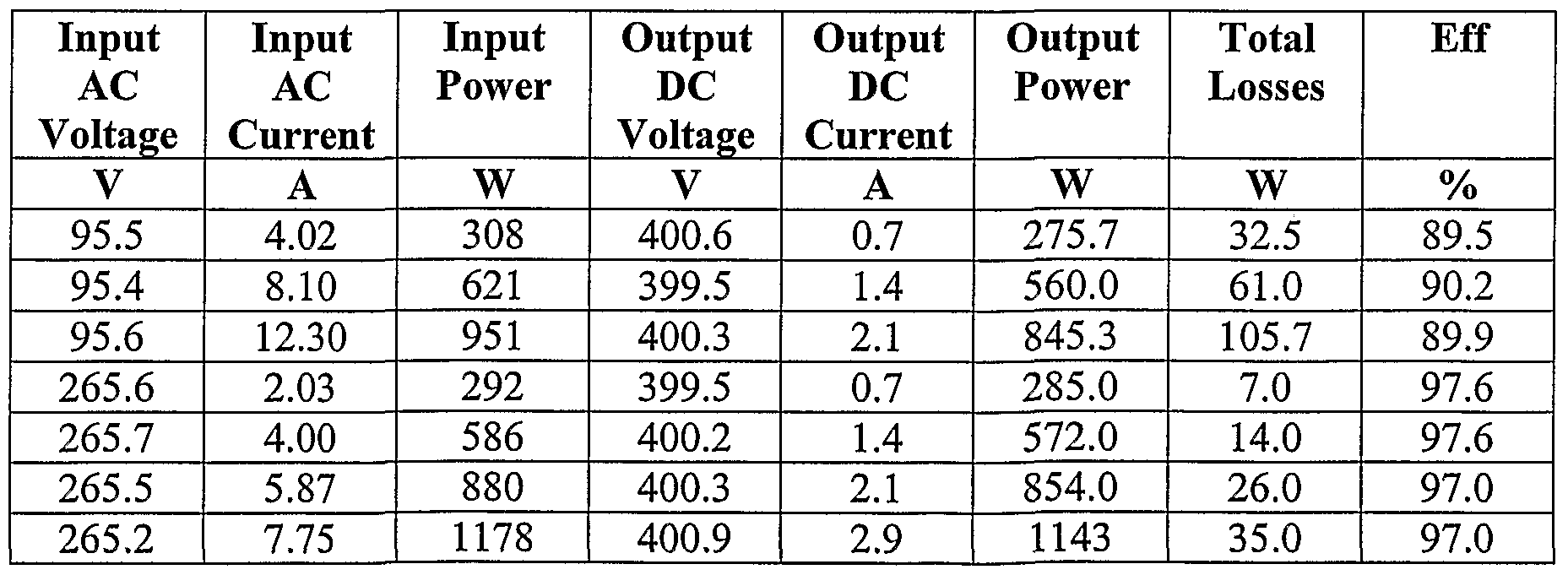
following Table 1 shows the switching losses of the input converter as a function of the input line voltage and load power. Table 1
Figure imgf000010_0001
[0056] The total input converter losses and efficiency were measured assuming the input voltage varying from a minimum of 95VRMS to a maximum of 265VRMS and 400VDC constant bus voltage. Tests were performed with a fixed switching frequency of 50KHz. The overall losses here reported are considered a worst case scenario since the tests were carried out with the switches being operated at constant duty cycle across the range of input voltage for the preset bus voltage. In a normal application the duty cycle (in the case of continuous mode operation) is variable, reducing substantially the switching loss components. The following Table 2 shows the results obtained.
Table 2
Figure imgf000010_0002
[0057] The test circuit of Fig. 7 was used to compare losses in a typical smart bridge configuration. In an actual PFC regulator, it is the practice to measure IGBT collector current independently of diode bridge current, as is done in the circuit of Fig. 8. [0058] Warp2 series IGBTs (International Rectifier Corp.) are the device of choice for this topology and offer a great simplification in the current measurement and feedback, allowing for example the placement of current sensing in series with the diodes circuit and hence sensing a continuous current free of the switching components. [0059] Fig. 8 shows another example of abridgeless boost inverter circuit, including current sensing. The PFC function requires controlling the current drawn from the mains and shaping it to match the input voltage waveform. To accomplish this, the current is sensed at two terminals Isense and fed to the control circuit (not shown) which supplies a control signal DRIVE. Current sensing is achieved in this example by one or more current shunt resistor(s) R3 connected between the node of the anodes of Dl and D2 and the node of the emitters of TRl and TR2. This arrangement is facilitated by the use of IGBT switches, rather than MOSFETs as in serial no. 10/953,344, because the free-wheeling diodes proved for the IGBT's are on separate chips, unlike the intrinsic body diode in the MOSFET structure. In this example, a common line COM is defined by the anodes of the diodes Dl and D2. The output capacitor C is provided between COM and a terminal V+ at the cathodes of the boost diodes D3 and D4.
[0060] Several additional criteria have been observed for the optimization of the bridgeless PFC to achieve improved performance. This goal can be addressed by selection of the IGBT gate driver. For efficient operation, it is important to minimize switching losses in the IGBTs.
[0061] A solid gate driver is able to operate at switching frequency >50KHz and produces fast rise and fall times <100nS (when loaded by two IRGB20B60) with Rg as low as 6.8ohms. This driver function can be obtained by the adoption of an IR4427 IC driver, which has the desired dynamic and current output capabilities. As with all power switching circuits and regulators, layout is critical; hence the possibility to offer a simple plug & play solution with an integrated power module housing the input converter topology, the current sensing and the gate driver is the right answer to help electronic engineers facing the challenges of power management issues. With only 2 IR IPM modules, is possible today to integrate all the functions and circuits to address the power management functions of a typical driver for air-conditioning application. [0062] Input converters with active PFC circuit and bridgeless topology, operating at high frequency, have been analyzed and power losses and efficiency advantages illustrated.
[0063] Benefits from these advancements have been shown, resulting in high efficiency converter operation, more than a 50% reduction in overall motor control system size, vastly reduced component counts, and reduced system cost and development time. [0064] The disclosed power factor power topology and advanced packaging will help engineers to resolve new power management challenges in appliance systems for climate control. Thus, the engineering challenge to provide energy-efficient variable speed motor drive, respecting the standards for power factor correction, is addressed simply and cost effectively.
[0065] Although the present invention has been described in relation to particular embodiments thereof, many other variations and modifications and other uses will become apparent to those skilled in the art. Therefore, the present invention is not limited by the specific disclosure herein.

Claims

WHAT IS CLAIMED IS:
1. A bridgeless PFC boost converter comprising: a boost inductor having a first end connected to a first AC input terminal and a second end connected to a first junction defined between the anode of a first diode and a first terminal of a first switch; a second terminal of the first switch connected to a common line; a parallel circuit of a capacitance and load terminals connected between the cathode of the first diode and the common line; a series circuit of a second diode and a second switch connected between the cathode of the first diode and the common line; a second AC input terminal connected to a second junction defined between the anode of the second diode and the second switch; and a control circuit connected for controlling the first and second switches so as to provide power factor correction with respect to power applied to said load terminals.
2. A bridgeless PFC boost converter according to claim 1, wherein said first and second switches are IGBTs.
3. A bridgeless PFC boost converter according to claim 1, further comprising another boost inductor connected between said second AC input terminal and said second junction.
4. A bridgeless PFC boost converter according to claim 1, further comprising respective third and fourth diodes connected in parallel with said first and second switches, their cathodes being connected to the corresponding said first and second junctions.
5. A bridgeless PFC boost converter according to claim 4, wherein said IGBTs each have a pair of main terminals connected respectively to said common line and to the corresponding one of said first and second junctions; and a gate terminal connected to said control circuit.
6. A bridgeless PFC boost converter according to claim 5, further comprising a resistance network interconnecting said control circuit, said gate terminals, and said common line.
7. A bridgeless PFC boost converter according to claim 4, wherein said control circuit controls said first and second switches in response to current in said first and second switches.
8. A bridgeless PFC boost converter according to claim 4, wherein said control circuit controls said first and second switches in response to voltage at said first and second AC input terminals and to an output voltage across said load terminals.
9. A bridgeless PFC boost converter according to claim 8, wherein said control circuit senses zero voltage crossing at said AC input terminals.
10. A bridgeless PFC boost converter according to claim 4, wherein the anodes of the third and fourth diodes are connected to the common line.
11. A bridgeless PFC boost converter according to claim 1 , wherein said control circuit controls said first and second switches in response to current in said first and second switches.
12. A bridgeless PFC boost converter according to claim 1 , wherein said control circuit controls said first and second switches in response to voltage at said first and second AC input terminals and to an output voltage across said load terminals.
13. A bridgeless PFC boost converter according to claim 12, wherein said control circuit senses zero voltage crossing at said AC input terminals.
14. A bridgeless PFC boost converter according to claim 1, further comprising respective third and fourth diodes connected in parallel with said first and second switches, having their cathodes connected respectively to said first and second AC input terminals.
15. A bridgeless PFC boost converter according to claim 14, further comprising another boost inductor connected between said second AC input terminal and said second junction.
16. A bridgeless PFC boost converter according to claim 1, wherein said second terminals of said first and second switches are connected to a sensing line which in turn is connected to said common line by a shunt resistor.
17. A bridgeless PFC boost converter according to claim 16, wherein the anodes of the third and fourth diodes are connected to the common line.
18. A bridgeless PFC boost converter according to claim 16, wherein said control circuit controls said first and second switches in response to voltages on said sensing line and said common line.
19. A boost type power supply circuit for providing a DC output voltage comprising: first and second semiconductor switches coupled between respective input lines and a common connection, an AC input voltage from an AC source being supplied across the input lines; first and second diodes coupled in series with respective ones of the switches; third and fourth diodes coupled across respective ones of the switches in a free-wheeling relationship with the switches, an inductance coupled in at least one of the input lines; a controller for controlling the conduction times of the switches by providing a pulse width control signal to each of the switches; whereby the controller turns on at least one of the switches during a positive half cycle of the AC voltage to allow energy storage in the inductance and turns off at least one switch to allow the energy stored in the inductance to be supplied to an attached load through one of the first and second diodes and one of the third and fourth diodes; and the controller turns on at least one of the switches during a negative half cycle of the AC voltage to allow energy storage in the inductance and turns off the at least one switch to allow the energy stored in the inductance to be supplied to the attached load through one of the first and second diodes and one of the third and fourth diodes; and wherein the controller determines an on-time and an off-time of a pulse of the pulse width modulated control signal during each half cycle of the AC voltage based on at least one input without requiring sensing of the input current from the AC source; the on-time and off-time of the pulse being controlled to regulate said output voltage and to provide power factor correction of said AC input voltage.
20. The circuit of claim 19, further comprising a detection circuit providing an input to said controller to determine a beginning of each half cycle of said AC voltage and wherein said on-times represent a first time period following said beginning of each half cycle and said off-times represent a second time period following said beginning of said half cycle, said pulse having a pulse width determined by the time difference between said on-time and said off-time; and said on-times and off-times being selected to provide power factor correction.
21. The circuit of claim 20, wherein said detection circuit to determine a beginning of each half cycle comprises a zero crossing voltage detection circuit.
22. The circuit of claim 21, wherein one of said inputs to said controller comprises an output of said zero crossing voltage detection circuit.
23. The circuit of claim 19, wherein the at least one input to said controller comprises a voltage related to the output voltage of said circuit, whereby the output voltage is regulated within a predefined regulation range by controlling said pulse width.
24. The circuit of claim 23, wherein the voltage related to the output voltage is developed across a voltage divider circuit.
25. The circuit of claim 23, wherein the at least one input comprises a signal determining the beginning of each half cycle of said AC input voltage, said controller providing a pulse width modulated signal with said determined on-time and off-time to provide power factor correction of said AC input voltage.
26. The circuit of claim 19, wherein said switches comprise IGBTs.
27. The circuit of claim 19, further comprising an output capacitor across which said output voltage is developed.
28. The circuit of claim 19, wherein said inductance comprises first and second inductors disposed in each of said input lines.
PCT/US2006/011556 2005-03-31 2006-03-30 Bridgeless boost converter with pfc circuit Ceased WO2006105247A2 (en)

Priority Applications (2)

Application Number Priority Date Filing Date Title
JP2008504329A JP2008535460A (en) 2005-03-31 2006-03-30 Boost converter with PFC circuit without bridge
EP06739998A EP1864372A2 (en) 2005-03-31 2006-03-30 Bridgeless boost converter with pfc circuit

Applications Claiming Priority (4)

Application Number Priority Date Filing Date Title
US66695005P 2005-03-31 2005-03-31
US60/666,950 2005-03-31
US11/392,039 2006-03-29
US11/392,039 US20060198172A1 (en) 2003-10-01 2006-03-29 Bridgeless boost converter with PFC circuit

Publications (3)

Publication Number Publication Date
WO2006105247A2 true WO2006105247A2 (en) 2006-10-05
WO2006105247A3 WO2006105247A3 (en) 2007-06-07
WO2006105247B1 WO2006105247B1 (en) 2007-07-19

Family

ID=37054105

Family Applications (1)

Application Number Title Priority Date Filing Date
PCT/US2006/011556 Ceased WO2006105247A2 (en) 2005-03-31 2006-03-30 Bridgeless boost converter with pfc circuit

Country Status (5)

Country Link
US (1) US20060198172A1 (en)
EP (1) EP1864372A2 (en)
KR (1) KR20070116240A (en)
TW (1) TW200643679A (en)
WO (1) WO2006105247A2 (en)

Cited By (7)

* Cited by examiner, † Cited by third party
Publication number Priority date Publication date Assignee Title
KR100992457B1 (en) 2008-05-08 2010-11-08 엘지이노텍 주식회사 Power factor correction circuit
EP2330732A1 (en) * 2009-12-03 2011-06-08 AEG Power Solutions B.V. Pre-load circuit for an AC/DC converter
US8279629B2 (en) 2009-07-29 2012-10-02 Tdk Corporation Switching power supply
CN102721848A (en) * 2011-03-29 2012-10-10 艾默生网络能源系统北美公司 Method and apparatus for detecting input current of bridgeless PFC circuit
US9214856B2 (en) 2012-12-05 2015-12-15 Samsung Electro-Mechanics Co., Ltd. Power factor correction device
US9270197B2 (en) 2012-12-05 2016-02-23 Samsung Electro-Mechanics Co., Ltd. Power factor correction apparatus and method for correcting power factor using the same
CN105490551A (en) * 2015-12-28 2016-04-13 华为技术有限公司 Circuit of uninterrupted power supply

Families Citing this family (54)

* Cited by examiner, † Cited by third party
Publication number Priority date Publication date Assignee Title
WO2005041393A2 (en) * 2003-10-24 2005-05-06 Pf1, Inc. Method and system for power factor correction
DE102005039867B4 (en) * 2005-08-23 2016-04-07 Power Systems Technologies Gmbh Input circuit for a switching power supply
US7518895B2 (en) * 2006-06-30 2009-04-14 Fairchild Semiconductor Corporation High-efficiency power converter system
US7903442B2 (en) * 2006-11-30 2011-03-08 Dell Products L.P. Apparatus and methods for power conversion
US20080284400A1 (en) * 2007-05-18 2008-11-20 Eric Gregory Oettinger Methods and apparatus to monitor a digital power supply
GB2452318A (en) * 2007-08-31 2009-03-04 Eltek Energy AC to DC bridgeless boost converter
US8950206B2 (en) 2007-10-05 2015-02-10 Emerson Climate Technologies, Inc. Compressor assembly having electronics cooling system and method
US20090241592A1 (en) * 2007-10-05 2009-10-01 Emerson Climate Technologies, Inc. Compressor assembly having electronics cooling system and method
US7895003B2 (en) 2007-10-05 2011-02-22 Emerson Climate Technologies, Inc. Vibration protection in a variable speed compressor
US8459053B2 (en) 2007-10-08 2013-06-11 Emerson Climate Technologies, Inc. Variable speed compressor protection system and method
US9541907B2 (en) 2007-10-08 2017-01-10 Emerson Climate Technologies, Inc. System and method for calibrating parameters for a refrigeration system with a variable speed compressor
US8448459B2 (en) 2007-10-08 2013-05-28 Emerson Climate Technologies, Inc. System and method for evaluating parameters for a refrigeration system with a variable speed compressor
US8539786B2 (en) 2007-10-08 2013-09-24 Emerson Climate Technologies, Inc. System and method for monitoring overheat of a compressor
US8418483B2 (en) 2007-10-08 2013-04-16 Emerson Climate Technologies, Inc. System and method for calculating parameters for a refrigeration system with a variable speed compressor
GB2455128B (en) 2007-11-29 2012-03-21 Eltek Valere As Control system and method for controlling a bridgeless boost converter
KR100946002B1 (en) * 2007-12-28 2010-03-09 삼성전기주식회사 Bridgeless Power Factor Correction Circuit
WO2009095836A2 (en) * 2008-01-29 2009-08-06 Philips Intellectual Property & Standards Gmbh Electronic driver circuit and method
US8199541B2 (en) * 2008-04-11 2012-06-12 System General Corp. High efficiency bridgeless PFC power converter
KR100952180B1 (en) * 2008-05-09 2010-04-09 엘지이노텍 주식회사 Power factor correction circuit
KR101463564B1 (en) * 2008-05-13 2014-11-21 엘지이노텍 주식회사 Circuit for power factor correction
US8614595B2 (en) * 2008-11-14 2013-12-24 Beniamin Acatrinei Low cost ultra versatile mixed signal controller circuit
EP2387817B1 (en) * 2009-01-14 2018-06-27 Nxp B.V. Pfc with high efficiency at low load
CN101599695A (en) * 2009-07-03 2009-12-09 中兴通讯股份有限公司 Bridgeless power factor correction circuit and its control method
US8264192B2 (en) 2009-08-10 2012-09-11 Emerson Climate Technologies, Inc. Controller and method for transitioning between control angles
US8508166B2 (en) 2009-08-10 2013-08-13 Emerson Climate Technologies, Inc. Power factor correction with variable bus voltage
TWI401869B (en) * 2009-09-25 2013-07-11 Univ Nat Taiwan Science Tech Single core two phases power factor correction apparatus, and driving method thereof
US8717791B2 (en) * 2009-09-30 2014-05-06 Astec International Limited Bridgeless boost PFC circuits and systems
US8531138B2 (en) * 2009-10-14 2013-09-10 National Semiconductor Corporation Dimmer decoder with improved efficiency for use with LED drivers
US9590495B2 (en) 2011-08-26 2017-03-07 Futurewei Technologies, Inc. Holdup time circuit and method for bridgeless PFC converter
KR101288201B1 (en) 2011-09-16 2013-07-18 삼성전기주식회사 Power factor correction circuit, power supply having thereof and motor driver
US9634593B2 (en) 2012-04-26 2017-04-25 Emerson Climate Technologies, Inc. System and method for permanent magnet motor control
WO2013188119A1 (en) * 2012-06-13 2013-12-19 Efficient Power Conversion Corporation Method for operating a non-isolated switching converter having synchronous rectification capability suitable for power factor correction applications
WO2014026124A1 (en) 2012-08-10 2014-02-13 Emerson Climate Technologies, Inc. Motor drive control using pulse-width modulation pulse skipping
US9660540B2 (en) 2012-11-05 2017-05-23 Flextronics Ap, Llc Digital error signal comparator
CN103809007A (en) * 2012-11-13 2014-05-21 中兴通讯股份有限公司 Device and method for inductive current sampling of bridge-free PFC circuit
KR101422939B1 (en) * 2012-12-05 2014-07-23 삼성전기주식회사 Deriver device for power factor correction circuit
KR101422947B1 (en) * 2012-12-11 2014-07-23 삼성전기주식회사 Power factor correction circuit and power supply having the same
CN103887962B (en) * 2012-12-20 2016-08-17 Tdk株式会社 Circuit of power factor correction
CN103066865B (en) * 2013-02-04 2016-02-24 电子科技大学 Three-phase Bridgeless power factor correction A.C.-D.C. converter
US9494658B2 (en) * 2013-03-14 2016-11-15 Flextronics Ap, Llc Approach for generation of power failure warning signal to maximize useable hold-up time with AC/DC rectifiers
US9323267B2 (en) 2013-03-14 2016-04-26 Flextronics Ap, Llc Method and implementation for eliminating random pulse during power up of digital signal controller
US9627915B2 (en) 2013-03-15 2017-04-18 Flextronics Ap, Llc Sweep frequency mode for multiple magnetic resonant power transmission
US20140354246A1 (en) * 2013-05-30 2014-12-04 Flextronics Ap, Llc Bridgeless pfc power converter with high efficiency
CN104300810B (en) * 2013-07-17 2017-05-17 台达电子企业管理(上海)有限公司 Power factor correction converter and control method
KR101465129B1 (en) * 2013-07-22 2014-11-26 인하대학교 산학협력단 Apparatus and method for power factor correction
US20150318780A1 (en) * 2013-11-07 2015-11-05 Marco Antonio Davila Bridgeless PFC Using Single Sided High Frequency Switching
CN103722276B (en) * 2013-12-27 2016-08-17 上海沪工焊接集团股份有限公司 A kind of inverter type welder peak point current feedback circuit
US9621053B1 (en) 2014-08-05 2017-04-11 Flextronics Ap, Llc Peak power control technique for primary side controller operation in continuous conduction mode
US9941799B1 (en) 2014-08-08 2018-04-10 Flextronics Ap, Llc Cascade power system with isolated Class-E resonant circuit
CN105091252B (en) * 2015-09-23 2018-06-29 广东美的制冷设备有限公司 The control method of pfc circuit, system and air conditioner in air conditioner
KR101711343B1 (en) * 2016-07-29 2017-03-02 동의대학교 산학협력단 Output current sensing method for single-phase grid-connected photovolataic inverters
TWI690143B (en) * 2019-04-02 2020-04-01 瑞昱半導體股份有限公司 Voltage converter
US11206743B2 (en) 2019-07-25 2021-12-21 Emerson Climate Technolgies, Inc. Electronics enclosure with heat-transfer element
CN111224447A (en) * 2020-02-27 2020-06-02 深圳威迈斯新能源股份有限公司 On-vehicle machine that charges of compatible alternating-current charging stake and direct-current charging stake

Family Cites Families (13)

* Cited by examiner, † Cited by third party
Publication number Priority date Publication date Assignee Title
US4412277A (en) * 1982-09-03 1983-10-25 Rockwell International Corporation AC-DC Converter having an improved power factor
DK382687A (en) * 1987-07-22 1989-04-14 Scanpower POWER SUPPLY CIRCUIT
DK173534B1 (en) * 1990-11-14 2001-02-05 Scanpower Power supply circuit with integrated magnetic components
US5793624A (en) * 1996-06-05 1998-08-11 Hydro-Quebec Apparatus and method for charging a DC battery
DE19839446A1 (en) * 1998-08-29 2000-03-02 Bosch Gmbh Robert Arrangement for detecting the angle of rotation of a rotatable element
US6320772B1 (en) * 1999-05-26 2001-11-20 Matsushita Electric Industrial Co., Ltd. Converter circuit having control means with capability to short-circuit converter output
DE19942794A1 (en) * 1999-09-08 2001-03-15 Philips Corp Intellectual Pty Converter with boost converter arrangement
US6456514B1 (en) * 2000-01-24 2002-09-24 Massachusetts Institute Of Technology Alternator jump charging system
US6411535B1 (en) * 2001-03-29 2002-06-25 Emc Corporation Power factor correction circuit with integral bridge function
TW550878B (en) * 2001-04-06 2003-09-01 Delta Electronics Inc Zero-voltage zero-current switching power factor correction converter
TWI261961B (en) * 2001-11-12 2006-09-11 Ind Tech Res Inst Active power factor correction circuit
US6738274B2 (en) * 2002-09-09 2004-05-18 Hewlett-Packard Development Company, L.P. Power supply with integrated bridge and boost circuit
US6853174B1 (en) * 2003-08-11 2005-02-08 Micrel, Inc. Selective high-side and low-side current sensing in switching power supplies

Cited By (9)

* Cited by examiner, † Cited by third party
Publication number Priority date Publication date Assignee Title
KR100992457B1 (en) 2008-05-08 2010-11-08 엘지이노텍 주식회사 Power factor correction circuit
US8279629B2 (en) 2009-07-29 2012-10-02 Tdk Corporation Switching power supply
EP2330732A1 (en) * 2009-12-03 2011-06-08 AEG Power Solutions B.V. Pre-load circuit for an AC/DC converter
FR2953663A1 (en) * 2009-12-03 2011-06-10 Aeg Power Solutions Bv PRE-CHARGE CIRCUIT FOR AC / DC CONVERTER
CN102721848A (en) * 2011-03-29 2012-10-10 艾默生网络能源系统北美公司 Method and apparatus for detecting input current of bridgeless PFC circuit
US9214856B2 (en) 2012-12-05 2015-12-15 Samsung Electro-Mechanics Co., Ltd. Power factor correction device
US9270197B2 (en) 2012-12-05 2016-02-23 Samsung Electro-Mechanics Co., Ltd. Power factor correction apparatus and method for correcting power factor using the same
CN105490551A (en) * 2015-12-28 2016-04-13 华为技术有限公司 Circuit of uninterrupted power supply
CN105490551B (en) * 2015-12-28 2018-07-03 华为技术有限公司 A kind of circuit of uninterruptible power supply

Also Published As

Publication number Publication date
TW200643679A (en) 2006-12-16
WO2006105247B1 (en) 2007-07-19
KR20070116240A (en) 2007-12-07
WO2006105247A3 (en) 2007-06-07
EP1864372A2 (en) 2007-12-12
US20060198172A1 (en) 2006-09-07

Similar Documents

Publication Publication Date Title
US20060198172A1 (en) Bridgeless boost converter with PFC circuit
Ki et al. A high step-down transformerless single-stage single-switch AC/DC converter
US20100259240A1 (en) Bridgeless PFC converter
US20040047167A1 (en) Power supply with integrated bridge and boost circuit
US10566891B2 (en) Power supply device and control method thereof
JP2008535460A (en) Boost converter with PFC circuit without bridge
JP2023052955A (en) Operation control method, circuit, home appliance and computer readable storage medium
Sasikala et al. Review of AC-DC power electronic converter topologies for power factor correction
Lee et al. Design of a GaN totem-pole PFC converter using DC-link voltage control strategy for data center applications
CN102684492B (en) High power factor converter
CN107733319A (en) Speed-adjusting circuit of alternating and air conditioner
EP2120320B1 (en) Dc power supply device
US20060139020A1 (en) Simple partial switching power factor correction circuit
CN111355431B (en) Motor drive control circuit, circuit board and air conditioner
CN110112902B (en) Three-phase boost-buck PFC rectification circuit
JP3670955B2 (en) Power factor correction circuit
JP2002330588A (en) Converter device
CN217545873U (en) Power factor correction circuit and electronic equipment
Consoli et al. Unipolar converter for switched reluctance motor drives with power factor improvement
CN111525822B (en) Switching power supply controller, switching power supply system and switching power supply system power supply method
CN114389462B (en) Current detection method and overcurrent protection method for alternating current chopper circuit
Jumadril et al. An improved two-switch bridgeless PFC SEPIC structure for total harmonic distortion reduction and circulating current minimization
Singh et al. A Zeta–Luo Integrated Dual Output Bridgeless Rectifier Fed SRM Drive With Improved Power Quality
KR102542284B1 (en) 4 Switch Buck-Boost Converter And Variable Hybrid Distribution Link Voltage System Including The Same
CN220359032U (en) Power factor corrector, power factor correction circuit and power supply equipment

Legal Events

Date Code Title Description
WWE Wipo information: entry into national phase

Ref document number: 200680010582.5

Country of ref document: CN

121 Ep: the epo has been informed by wipo that ep was designated in this application
WWE Wipo information: entry into national phase

Ref document number: 2006739998

Country of ref document: EP

WWE Wipo information: entry into national phase

Ref document number: 1020077022117

Country of ref document: KR

ENP Entry into the national phase

Ref document number: 2008504329

Country of ref document: JP

Kind code of ref document: A

NENP Non-entry into the national phase

Ref country code: DE

NENP Non-entry into the national phase

Ref country code: RU