WO2006117954A1 - Al-Ni-B合金配線材料及びそれを用いた素子構造 - Google Patents
Al-Ni-B合金配線材料及びそれを用いた素子構造 Download PDFInfo
- Publication number
- WO2006117954A1 WO2006117954A1 PCT/JP2006/306676 JP2006306676W WO2006117954A1 WO 2006117954 A1 WO2006117954 A1 WO 2006117954A1 JP 2006306676 W JP2006306676 W JP 2006306676W WO 2006117954 A1 WO2006117954 A1 WO 2006117954A1
- Authority
- WO
- WIPO (PCT)
- Prior art keywords
- wiring material
- alloy
- layer
- semiconductor layer
- wiring circuit
- Prior art date
- Legal status (The legal status is an assumption and is not a legal conclusion. Google has not performed a legal analysis and makes no representation as to the accuracy of the status listed.)
- Ceased
Links
Classifications
-
- H—ELECTRICITY
- H10—SEMICONDUCTOR DEVICES; ELECTRIC SOLID-STATE DEVICES NOT OTHERWISE PROVIDED FOR
- H10D—INORGANIC ELECTRIC SEMICONDUCTOR DEVICES
- H10D30/00—Field-effect transistors [FET]
- H10D30/60—Insulated-gate field-effect transistors [IGFET]
- H10D30/67—Thin-film transistors [TFT]
- H10D30/6729—Thin-film transistors [TFT] characterised by the electrodes
- H10D30/6737—Thin-film transistors [TFT] characterised by the electrodes characterised by the electrode materials
-
- C—CHEMISTRY; METALLURGY
- C22—METALLURGY; FERROUS OR NON-FERROUS ALLOYS; TREATMENT OF ALLOYS OR NON-FERROUS METALS
- C22C—ALLOYS
- C22C21/00—Alloys based on aluminium
-
- C—CHEMISTRY; METALLURGY
- C22—METALLURGY; FERROUS OR NON-FERROUS ALLOYS; TREATMENT OF ALLOYS OR NON-FERROUS METALS
- C22C—ALLOYS
- C22C21/00—Alloys based on aluminium
- C22C21/10—Alloys based on aluminium with zinc as the next major constituent
-
- C—CHEMISTRY; METALLURGY
- C23—COATING METALLIC MATERIAL; COATING MATERIAL WITH METALLIC MATERIAL; CHEMICAL SURFACE TREATMENT; DIFFUSION TREATMENT OF METALLIC MATERIAL; COATING BY VACUUM EVAPORATION, BY SPUTTERING, BY ION IMPLANTATION OR BY CHEMICAL VAPOUR DEPOSITION, IN GENERAL; INHIBITING CORROSION OF METALLIC MATERIAL OR INCRUSTATION IN GENERAL
- C23C—COATING METALLIC MATERIAL; COATING MATERIAL WITH METALLIC MATERIAL; SURFACE TREATMENT OF METALLIC MATERIAL BY DIFFUSION INTO THE SURFACE, BY CHEMICAL CONVERSION OR SUBSTITUTION; COATING BY VACUUM EVAPORATION, BY SPUTTERING, BY ION IMPLANTATION OR BY CHEMICAL VAPOUR DEPOSITION, IN GENERAL
- C23C14/00—Coating by vacuum evaporation, by sputtering or by ion implantation of the coating forming material
- C23C14/22—Coating by vacuum evaporation, by sputtering or by ion implantation of the coating forming material characterised by the process of coating
- C23C14/34—Sputtering
- C23C14/3407—Cathode assembly for sputtering apparatus, e.g. Target
- C23C14/3414—Metallurgical or chemical aspects of target preparation, e.g. casting, powder metallurgy
-
- H—ELECTRICITY
- H05—ELECTRIC TECHNIQUES NOT OTHERWISE PROVIDED FOR
- H05B—ELECTRIC HEATING; ELECTRIC LIGHT SOURCES NOT OTHERWISE PROVIDED FOR; CIRCUIT ARRANGEMENTS FOR ELECTRIC LIGHT SOURCES, IN GENERAL
- H05B1/00—Details of electric heating devices
- H05B1/02—Automatic switching arrangements specially adapted to apparatus ; Control of heating devices
-
- H—ELECTRICITY
- H10—SEMICONDUCTOR DEVICES; ELECTRIC SOLID-STATE DEVICES NOT OTHERWISE PROVIDED FOR
- H10D—INORGANIC ELECTRIC SEMICONDUCTOR DEVICES
- H10D30/00—Field-effect transistors [FET]
- H10D30/60—Insulated-gate field-effect transistors [IGFET]
- H10D30/67—Thin-film transistors [TFT]
- H10D30/6729—Thin-film transistors [TFT] characterised by the electrodes
- H10D30/6737—Thin-film transistors [TFT] characterised by the electrodes characterised by the electrode materials
- H10D30/6739—Conductor-insulator-semiconductor electrodes
-
- H—ELECTRICITY
- H10—SEMICONDUCTOR DEVICES; ELECTRIC SOLID-STATE DEVICES NOT OTHERWISE PROVIDED FOR
- H10D—INORGANIC ELECTRIC SEMICONDUCTOR DEVICES
- H10D30/00—Field-effect transistors [FET]
- H10D30/60—Insulated-gate field-effect transistors [IGFET]
- H10D30/67—Thin-film transistors [TFT]
- H10D30/674—Thin-film transistors [TFT] characterised by the active materials
- H10D30/6741—Group IV materials, e.g. germanium or silicon carbide
- H10D30/6743—Silicon
-
- H—ELECTRICITY
- H10—SEMICONDUCTOR DEVICES; ELECTRIC SOLID-STATE DEVICES NOT OTHERWISE PROVIDED FOR
- H10D—INORGANIC ELECTRIC SEMICONDUCTOR DEVICES
- H10D86/00—Integrated devices formed in or on insulating or conducting substrates, e.g. formed in silicon-on-insulator [SOI] substrates or on stainless steel or glass substrates
- H10D86/40—Integrated devices formed in or on insulating or conducting substrates, e.g. formed in silicon-on-insulator [SOI] substrates or on stainless steel or glass substrates characterised by multiple TFTs
- H10D86/441—Interconnections, e.g. scanning lines
-
- H—ELECTRICITY
- H10—SEMICONDUCTOR DEVICES; ELECTRIC SOLID-STATE DEVICES NOT OTHERWISE PROVIDED FOR
- H10D—INORGANIC ELECTRIC SEMICONDUCTOR DEVICES
- H10D86/00—Integrated devices formed in or on insulating or conducting substrates, e.g. formed in silicon-on-insulator [SOI] substrates or on stainless steel or glass substrates
- H10D86/40—Integrated devices formed in or on insulating or conducting substrates, e.g. formed in silicon-on-insulator [SOI] substrates or on stainless steel or glass substrates characterised by multiple TFTs
- H10D86/60—Integrated devices formed in or on insulating or conducting substrates, e.g. formed in silicon-on-insulator [SOI] substrates or on stainless steel or glass substrates characterised by multiple TFTs wherein the TFTs are in active matrices
-
- H—ELECTRICITY
- H10—SEMICONDUCTOR DEVICES; ELECTRIC SOLID-STATE DEVICES NOT OTHERWISE PROVIDED FOR
- H10P—GENERIC PROCESSES OR APPARATUS FOR THE MANUFACTURE OR TREATMENT OF DEVICES COVERED BY CLASS H10
- H10P14/00—Formation of materials, e.g. in the shape of layers or pillars
- H10P14/40—Formation of materials, e.g. in the shape of layers or pillars of conductive or resistive materials
- H10P14/42—Formation of materials, e.g. in the shape of layers or pillars of conductive or resistive materials using a gas or vapour
Definitions
- the present invention relates to an A1-based alloy wiring material used for an element of a display device such as a liquid crystal display, and in particular, an Al—Ni—B alloy wiring material suitable for a display device including a thin film transistor and a transparent electrode. It relates to the element structure used.
- A1 aluminum
- A1-based alloy wiring materials made of aluminum (hereinafter sometimes simply referred to as “A1”) alloy have been widely used as a constituent material for display devices such as thin-screen televisions typified by liquid crystal displays.
- the reason for this is that the specific resistance value of the A1-based alloy wiring material is low and the wiring process is easy.
- TFT thin film transistor
- ITO Indium Tin Oxide
- IZO Indium Zinc Oxide
- An element is composed of a transparent electrode (hereinafter sometimes referred to as a transparent electrode layer) and a wiring circuit (hereinafter also referred to as a wiring circuit layer) formed from an A1-based alloy wiring material.
- a transparent electrode hereinafter sometimes referred to as a transparent electrode layer
- a wiring circuit hereinafter also referred to as a wiring circuit layer
- n + -Si phosphorus-doped semiconductor layer
- the wiring circuit and the transparent A refractory metal material such as molybdenum (Mo) or titanium (Ti) is formed between the electrodes as a so-called cap layer.
- the thermal process during the manufacturing process prevents the interdiffusion of A1 and Si between the semiconductor layer and the wiring circuit.
- the same refractory metal material such as molybdenum (Mo) and titanium (Ti) as the cap layer is interposed! /.
- FIG. Figure 1 shows a schematic cross-sectional view of an a-Si TFT for a liquid crystal display.
- This TFT structure In this case, an electrode wiring circuit layer 2 made of an A1-based alloy wiring material constituting the gate electrode portion G and a cap layer 3 having a force such as Mo and Mo—W are formed on the glass substrate 1.
- the gate electrode portion G is provided with a SiNx gate insulating film 4 as a protection. Further, on this gate insulating film 4, an a-Si semiconductor layer 5, a channel protective film layer 6, an n + -Si semiconductor layer 7, a cap layer 3, an electrode wiring circuit layer 2, and a cap layer 3 are sequentially deposited.
- a drain electrode portion D and a source electrode portion S are provided by appropriately forming a pattern.
- the drain electrode portion D and the source electrode portion S are covered with a surface flattening resin or SiNx insulating film 4. Further, on the source electrode portion S side, a contact hole CH is provided in the insulating layer 4, and a transparent electrode layer 7 ′ of ITO or IZO is formed in that portion.
- Patent Document 1 Japanese Unexamined Patent Publication No. 2003-89864
- an A1-based alloy wiring material that satisfies the following characteristics is required.
- Gate in the device structure of Figure 1 For the electrode wiring circuit layer 2 of the electrode G, it is necessary to be able to directly join with a transparent electrode layer such as ITO in the lead-out wiring portion, although not shown in the drawing, and preferably satisfy heat resistance of 350 ° C or higher. Is required. The reason is that a high temperature thermal history is added when forming the gate insulating film formed on the gate electrode G, so that the electrode wiring circuit layer causes defects such as hillocks even at a temperature of 350 ° C or higher. This is because there is a need for such heat resistance.
- the electrode wiring circuit layer 2 of the drain electrode portion D and the source electrode portion S in the element structure of FIG. 1 can be directly joined to a transparent electrode layer such as ITO, and n + -Si or the like It is required that direct bonding with the semiconductor layer is possible. In direct bonding with a semiconductor layer such as n + -Si, diffusion of A1 and Si is not required even when a thermal history of 200 ° C or higher is applied. Further, the electrode wiring circuit layer 2 of the drain electrode portion D and the source electrode portion S is required to have heat resistance that does not cause defects such as hillocks even when a thermal history of about 250 ° C. is applied.
- the A1 alloy wiring material that forms the gate electrode part G, drain electrode part D, source electrode part S and other wiring parts naturally has a low specific resistance, that is, 10 ⁇ 'cm.
- a specific resistance value that is, 5 ⁇ 'cm or less.
- A1 alloy wiring materials that satisfy all of these required characteristics are highly desired! This is the current situation.
- Patent Document 2 Japanese Patent Application Laid-Open No. 2004-214606
- the present invention has been made against the background described above, and in a display device including a thin film transistor and a transparent electrode layer, direct contact with a transparent electrode layer such as ITO or IZO is possible. At the same time, it provides A1 alloy wiring materials that can be directly bonded to semiconductor layers such as n + -Si.
- a display device element having a structure in which a wiring circuit layer formed of an A1-based alloy wiring material is directly bonded to a transparent electrode layer or a semiconductor layer, an increase in contact resistance value or a bonding failure when directly bonded is achieved. We propose an element structure of a display device that does not occur.
- the nickel content is the atomic percentage Xat% of nickel
- the boron content is the atomic percentage Yat%.
- Al—Ni— ⁇ alloy wiring material that is in the range of the area satisfying each of the formulas, with the balance being aluminum.
- the Al—Ni—B alloy wiring material in the present invention may be mixed in, for example, a material manufacturing process, a wiring circuit forming process, an element manufacturing process, or the like, as long as it does not deviate from the effects described below. It does not prevent the mixing of certain gas components and other inevitable impurities.
- Nickel has an effect of forming an intermetallic compound with aluminum by heat treatment to improve bonding characteristics in direct bonding with the transparent electrode layer.
- high nickel content As a result, the specific resistance of the wiring circuit itself becomes high and becomes impractical.
- the nickel content if the nickel content is low, the amount of intermetallic compounds produced with aluminum decreases, making direct bonding to the transparent electrode layer impossible, and heat resistance (a deterrent effect against the occurrence of plastic deformation of the A1-based alloy wiring material due to heat). ) Also tends to decrease. For these reasons, the nickel content must satisfy the above formula (1).
- the nickel content exceeds 10.0 &%, the specific resistance value of the wiring material becomes too large and a dimple-like defect called dimple is easily formed on the surface of the wiring material. There is a tendency that heat resistance cannot be secured.
- a so-called hillock protrusion is likely to be formed on the surface of the wiring material, and heat resistance tends not to be ensured.
- This dimple is a micro-dent-like defect formed on the surface of the material due to stress strain generated when heat-treating the A1 alloy wiring material. When this dimple is generated, it adversely affects the bonding characteristics and Reliability decreases.
- hillocks are the opposite of dimples, and are forces that are projections formed on the surface of the material due to the stress and strain generated when heat-treating an A1-based alloy wiring material. This will adversely affect the bonding reliability.
- These dimples and hillocks are common in that they are plastic deformation of the A1 alloy wiring material due to heat. This phenomenon is collectively called stress migration.
- A1 alloy wiring material depends on the level of occurrence of these defects. The heat resistance of can be judged.
- the inventors of the present application reliably prevent mutual diffusion of A1 and Si at the bonding interface even in a thermal process at a temperature exceeding 240 ° C when directly bonded to the semiconductor layer. In order to do so, it was found that the above formula (3) must be satisfied. They found that the above formula (4) must be satisfied in order to reliably maintain the specific resistance of the Al—Ni—B alloy wiring material itself at 10 ⁇ cm or less.
- the dimple is a minute dent-like defect formed on the surface of the wiring material when the Al—Ni—B alloy wiring material is heat-treated. After performing the prescribed heat treatment on the Ni-B alloy wiring material, the surface of the material was observed and the generated dimples (0.3 to 0.5 m) were investigated. In this dimple investigation, the area of all the dimples generated in the observation field of view was obtained, and the area ratio of the dimples in the observation field of view was used as the dimple generation rate.
- the above-mentioned (1) to (4 ) If the nickel content is 4.0% or more and the boron content is 0.80at% or less within the range satisfying the formula, dimple generation occurs even when heat treatment is performed at 350 ° C for 30 minutes. It was found that the survival rate can be suppressed to 1.6% or less. It is desirable that this dimple should not be generated as much as possible. If this dimple generation rate is low, even if it passes through a thermal process in the element manufacturing process of the display device, it is a bonded interface directly bonded to the semiconductor layer or transparent electrode layer. In this case, a bonding defect or the like is generated, and the bonding reliability is improved.
- the dimple generation rate is suppressed to 1.6% or less, for example, the on / off ratio (onZoff ratio) of a TFT having a structure directly bonded to a semiconductor layer is stabilized, and connection reliability is improved. It is considered a thing.
- the Al—Ni—B alloy wiring material according to the present invention is suitable for direct bonding to a semiconductor layer or a transparent electrode layer, for example, a high melting point metal material such as Mo is applied to the semiconductor layer side. Cap layer This does not prevent application in the provided element structure.
- the A1-Ni-B alloy wiring material according to the present invention according to the present invention as a so-called reflective film. .
- the inventors of the present application among the ranges satisfying the above formulas (1) to (4), the nickel content is 4.0 at% to 6. Oat% and the boron content is 0.20 at%. It was found that when it is ⁇ 0.8 at%, it becomes a particularly suitable Al—Ni—B alloy wiring material when directly bonding to a semiconductor layer.
- This deteriorated layer tends to be generated more easily as the heat treatment temperature becomes higher, and it is desirable that the deteriorated layer should not be generated by heat treatment (30 minutes) at 200 ° C. or higher.
- the nickel content is 4.0 at% to 6. Oat%, and boron is contained.
- the specific resistance of the wiring material itself is 5 ⁇ cm or less.
- the nickel content is 4.0 at% to 6. Oat% in the range satisfying the above formulas (1) to (4). If the boron content is in the composition range of 0.20 at% to 0.80 at%, when the semiconductor layer surface roughness value before direct bonding is 1, the semiconductor layer that is directly bonded and exposed after heat treatment is exposed. It was further found that the surface roughness value can be changed by 1.5 times or less.
- the amount of change in the surface roughness of the semiconductor layer is not clearly understood as a parameter directly related to the interdiffusion between Si and A1, the higher the heat treatment temperature, the more It has been confirmed that the amount of change is large.
- changes in the surface state of the semiconductor layer are expected to affect the switching characteristics of TFTs. In other words, it is presumed that this leads to a change in the on / off ratio (onZoff ratio) in the TFT, and the surface state of the semiconductor layer does not change much even if heat treatment is performed with direct bonding to the semiconductor layer. It is expected that the switching characteristics can be maintained well.
- the surface roughness Rz of the semiconductor layer exposed by peeling off the A1-based alloy wiring material is set to 1 when the surface roughness value of the semiconductor layer before direct bonding is 1.
- a change of 1.5 times or less of the previous semiconductor layer surface roughness value is considered to ensure sufficient connection reliability in consideration of TFT switching characteristics.
- the surface roughness Rz is adopted when specifying the surface state, but the surface property parameters described in JIS B0601 etc.
- parameters such as surface roughness Ra (arithmetic mean roughness) can be employed.
- the inventors of the present application relate to an element structure of a display device having a structure in which an A1-based alloy wiring material is directly bonded to a transparent electrode layer or a semiconductor layer.
- the surface roughness Ra of the A1-based alloy film was studied as a cause of poor bonding, and the A1—Ni—B alloy constituting the wiring circuit directly bonded to the semiconductor layer and Z or transparent electrode layer was studied.
- the surface roughness Ra of the Al—Ni—B alloy film formed from the Al-based alloy wiring material of the present invention is less than 2.OA, the bonding strength is low when the transparent electrode layer is directly bonded, 20. Above OA, it was found that the tendency of contact resistance value to increase was prominent.
- the surface roughness Ra is the surface roughness of the Al—Ni—B alloy film after film formation.
- the deposited Al-Ni-B alloy film has a structure in which a semiconductor layer is further formed in the case of a staggered structure or a transparent electrode layer is formed in the case of an inverted staggered structure. .
- the surface roughness Ra is obtained by performing non-contact measurement with an atomic force microscope (AFM) and calculating Ra according to JIS B0601-1982.
- the film thickness is 1000 A to 3000 A. If the Al—Ni—B alloy film thickness is less than 1000 A, it will be difficult for the effective resistance value when the wiring circuit is formed to satisfy a practical level, and if it exceeds 3000 A, the Al—Ni—B This is because the coverage of the upper layer laminated on the alloy film becomes non-uniform, and it tends to be difficult to form a practical element structure.
- the wiring circuit layer formed of the Al—Ni—B alloy wiring material of the present invention is dispersed and precipitated in the wiring circuit layer when the element is formed. It was found that the precipitates were uniformly dispersed without segregation.
- the proper shape can be obtained due to the difference in etching speed between the part where the prayer is generated and the part where no segregation occurs. It may happen that a wiring circuit cannot be formed.
- the wiring circuit layer formed of the Al—Ni—B alloy wiring material of the present invention when the element is constituted, Ni compound is dispersed and precipitated. On the line segment perpendicular to the wiring circuit layer thickness direction in the section of the wiring circuit layer, the abundance ratio is 25% to 45% in the thickness direction of the wiring circuit layer. In other words, the Ni composite does not tend to segregate over the entire thickness of the wiring circuit layer (see Fig. 6). Therefore, it is not necessary to specify the location where the transparent electrode layer or semiconductor layer is directly bonded, as in the A 1 Ni—Nd alloy wiring material described above, and a wiring circuit having an appropriate circuit shape can be reliably formed by etching. It becomes.
- Ni compound dispersed and precipitated in the wiring circuit layer formed of the Al—Ni—B alloy wiring material according to the present invention is mainly an Al Ni phase intermetallic compound.
- the present inventors are Ni compounds
- the nickel content is set to an atomic percentage Xat% of nickel, and the boron content is set to boron atoms.
- the percentage is Yat%, it is preferable to use a sputtering target that is in the range of the region satisfying the above formulas (1) to (4) and the balance being aluminum.
- the nickel content is 4.0 at% to 6. Oat% and the boron content is 0.20 at% to 0.80 at%. If it is a target, a wiring circuit that is extremely suitable for direct bonding to a semiconductor layer can be easily realized.
- a sputtering target having such a composition is used, an Al—Ni—B alloy thin film having almost the same composition as the force target composition, which may be somewhat affected by the film formation conditions during sputtering, can be easily formed.
- a wiring circuit may be formed by the aerosol deposition method using alloy particles having the A1—Ni—B alloy composition power of the present invention, which may be a dry method such as vapor deposition or spray homing, as a wiring material. And forming a wiring circuit by an ink jet method.
- FIG. 1 is a schematic sectional view of a TFT.
- FIG. 4 is a schematic oblique view of a test sample in which an ITO (IV) electrode layer and an Al alloy electrode layer are crossed and laminated.
- FIG. 5 Schematic of TEM observation photograph in the case of A1-2. Oat% Ni- Oat% Nd alloy.
- FIG. 6 Schematic of TEM observation photograph in the case of A1-5. Oat% Ni-0. 4at% B alloy.
- FIG. 7 is a measurement graph of the abundance ratio of Ni compounds.
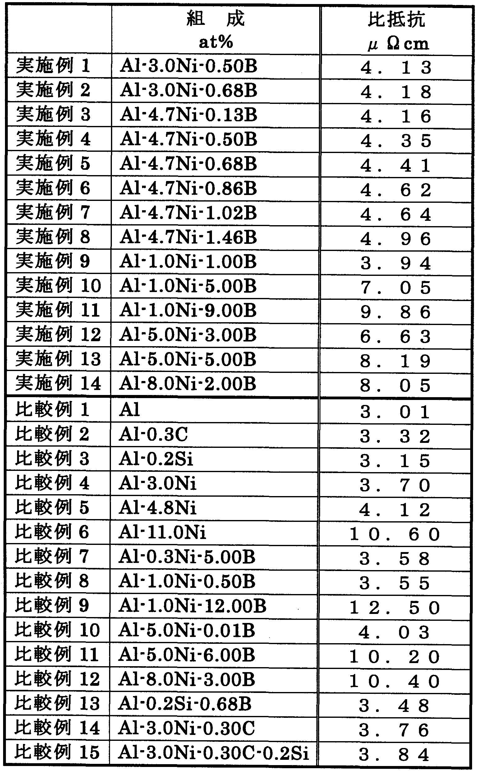
- A1—Ni—B alloy wiring materials having respective compositions of the examples and comparative examples shown in Table 1 were formed by sputtering, and the characteristics of the films were evaluated.
- the sputtering target was prepared by mixing aluminum with metals of each composition shown in Table 1, dissolving and stirring in a vacuum, forging in an inert gas atmosphere, rolling and molding the obtained ingot, A surface produced by processing the surface to be sputtered was used.
- the characteristics of the film in each composition listed in Table 1 are as follows: Si diffusion heat resistance when directly bonded to the semiconductor layer, specific resistance of the film, 350 ° C heat resistance of the film, ITO contact when directly bonded to the transparent electrode layer Conformity and IZO bondability were performed. The results are shown in Tables 1 and 2. [0036] [Table 1]
- Example 1 2 4 0 ⁇ ⁇ ⁇ Example 2 2 4 0 ⁇ ⁇ ⁇ Example 3 3 0 0 ⁇ ⁇ ⁇ Example 4 3 3 0 ⁇ ⁇ ⁇ Example 5 3 3 0 ⁇ ⁇ ⁇ Example 6 3 3 0 ⁇ ⁇ ⁇ Example 7 3 3 0 ⁇ ⁇ ⁇ Example 8 3 3 0 ⁇ ⁇ ⁇ Example 9 2 4 0 ⁇ ⁇ ⁇ Example 10 2 6 0 ⁇ ⁇ ⁇ Example 11 3 0 0 ⁇ ⁇ ⁇ Example 12 3 3 3 0 ⁇ ⁇ ⁇ Example 13 3 3 0 ⁇ ⁇ ⁇ Example 14 3 3 0 ⁇ ⁇ ⁇ Comparative Example 1 1 7 0 XXX Comparative Example 2 1 7 0 XXX Comparative Example 3 1 8 0 XXX Comparative Example 4 2 0 0 X ⁇ ⁇ Comparative Example 5 2 5 0 X ⁇ ⁇ Comparative Example 6 3 0 0 X ⁇ ⁇ Comparative Example
- Si diffusion heat resistance As an evaluation sample of this property, an n — Si semiconductor layer (30 OA) is formed on a glass substrate by CVD, and sputtering is performed on the semiconductor layer (magnetron sputtering equipment, input power 3.OWatt / cm 2 , an argon gas flow rate of 100 sccm, and an argon pressure of 0.5 Pa) were used in which each composition film (2000 A) shown in Table 1 was formed. Then, after setting the heat treatment temperature of the evaluation sample every 10 ° C in the temperature range of 150 to 350 ° C and performing heat treatment for 30 minutes in a nitrogen gas atmosphere, the phosphoric acid-based A1 etching solution (Kanto Made by Gakaku Co., Ltd.
- A1 mixed acid etchant with liquid temperature of 32 ° C Z composition (volume ratio) Phosphoric acid: succinic acid: acetic acid: water 16: 1: 2: 1 Only each of the composition films was dissolved to expose the semiconductor layer. The exposed surface of the semiconductor layer was observed with an optical microscope (200 times) to investigate whether or not interdiffusion between Si and A1 occurred.
- FIG. 2 and FIG. 3 show representative optical micrographs on the exposed semiconductor layer surface.
- Fig. 2 shows the surface of the semiconductor layer where no interdiffusion is observed
- Fig. 3 shows traces of interdiffusion (black spots in the photo).
- Si diffusion heat resistance the sample with black spots as shown in Fig. 3 is regarded as defective, and among the samples with no mutual diffusion as shown in Fig. 2, the highest heat treatment temperature value is set to Si diffusion heat resistance.
- Table 2 shows the index values for sex assessment.
- Specific resistance of film The specific resistance value of each composition film shown in Table 1 is obtained by forming a single film (thickness of about 0.3 m) on a glass substrate by sputtering (conditions are the same as above), After heat treatment at 300 ° C. for 30 minutes in a gas atmosphere, the measurement was performed with a four-terminal resistance measuring device.
- Heat resistance at 350 ° C The heat resistance of each composition film described in Table 1 is that a single film (thickness of about 0.3 m) is formed on a glass substrate by sputtering (the conditions are the same as above), and nitrogen is added.
- the film surface was observed with a scanning electron microscope (SEM: 10,000 times) after heat treatment for 30 minutes at a temperature in the range of 100 ° C to 400 ° C in a gas atmosphere.
- SEM scanning electron microscope
- ITO bonding property This ITO bonding property forms a ⁇ (In O-10wt% SnO) electrode layer (1000 A thickness, circuit width 10 m) on a glass substrate as shown in the schematic perspective view of FIG. And each on it
- Evaluation was made using a test sample (Kelvin device) formed so as to cross the composition film layer (2000 A thickness, circuit width 10 ⁇ m).
- an A1 alloy film having a thickness of 2000 A was formed on a glass substrate under the sputtering conditions using each A1 alloy target having the above composition.
- the substrate temperature during sputtering was set as shown in Table 6 to perform each film formation.
- the surface of each A1 alloy film is coated with a resist (OFPR800: Tokyo Ohka Kogyo Co., Ltd.), and a pattern film for forming a 10 m wide circuit is placed on the surface and exposed to light. .
- the film was developed with an alkali developer containing C tetramethylammonium and id-oxide (hereinafter abbreviated as TMAH developer).
- circuit formation is performed with a phosphoric acid mixed acid etching solution (manufactured by Kanto Chemical Co., Ltd.), and the resist is removed with a dimethyl sulfoxide (hereinafter abbreviated as DMSO) stripping solution.
- DMSO dimethyl sulfoxide
- the substrate on which the 10 ⁇ m-wide A1 alloy film circuit was formed was subjected to pure water cleaning and drying treatment, and an SiNx insulating layer (thickness 4200 A) was formed on the surface.
- This insulating layer was formed using a sputtering device under sputtering conditions of input power RF3.OWatt / cm 2 , argon gas flow rate 90 sccm, nitrogen gas flow rate 10 sccm, pressure 0.5 Pa, substrate temperature 300 ° C.
- a positive resist manufactured by Tokyo Ohka Kogyo Co., Ltd .: TFR-970
- a pattern film for opening a contact hole of 10 m ⁇ 10 m square is arranged to perform an exposure process.
- TMAH developer CF dry etching gas
- Contact hole formation condition is CF gas flow rate 5
- the pressure was 0 sccm
- the oxygen gas flow rate was 5 sccm
- the pressure was 4.0 Pa
- the output was 150 W.
- the resist was stripped with the DMSO stripper described above. Then, the remaining stripping solution was removed using isopropyl alcohol, and then washed with water and dried. For each sample after the resist removal process, the ITO target (composition In O-10wt% Sn
- the bright electrode layer was formed by sputtering (substrate temperature 70 ° C, input power 1.8 WattZcm 2 , argon gas flow rate 80 sccm, oxygen gas flow rate 0.7 sccm, pressure 0.37 Pa), and an ITO film with a thickness of 100 A was formed. Formed.
- the ITO film surface is coated with a resist (manufactured by Tokyo Ohka Kogyo Co., Ltd .: OFPR800), exposed by placing a pattern film, developed with TMAH developer, and oxalic acid mixed acid.
- a 10 m wide circuit was formed with an etching solution (manufactured by Kanto Chemical Co., Ltd .: ITO05N).
- the resist was removed with a DMSO stripping solution.
- Each test sample obtained by the manufacturing method as described above was subjected to a heat treatment at 250 ° C for 30 minutes in the air atmosphere.
- the resistance was measured by energization (3 mA).
- the resistance measurement conditions at this time were the so-called life acceleration test conditions in an atmosphere of 85 ° C.
- life acceleration test conditions the time (failure time) during which each test sample changed to a resistance value that was 100 times the initial resistance value at the start of measurement was examined.
- a test sample that failed even after 250 hours under this accelerated life test condition was rated as “Good”.
- the test sample that failed in 250 hours or less under the accelerated life test conditions was designated as evaluation X.
- JIS C 5003 1974, reference (book title “Efficient method of accelerated reliability test and its practice”: edited by Yoji Kanuma, publisher, Japan Techno Center Co., Ltd.) ).
- IZO bondability This IZO bondability is similar to the IZO bondability evaluation described above.
- Test sample (Kelvin device) formed to cross each A1 alloy film layer (2000 A thickness, circuit width 50 ⁇ m) on the electrode layer (1000 A thickness, circuit width 50 ⁇ m) was used to evaluate.
- the test sample was prepared under the same conditions as the ITO bondability.
- the resistance of this test sample was measured under the same life acceleration test conditions as in the case of the ITO bondability, and IZO bondability was evaluated from the results of the life acceleration test.
- the evaluation criteria were the same as the ITO bondability.
- the specific resistance value is 10 ⁇ cm or less, and Comparative Example 9 out of the composition range of the present invention is compared. In Example 11 and Comparative Example 12, the specific resistance value exceeded 10 ⁇ cm. Also shown in Table 2. As can be seen, the Al-Ni-B alloy wiring material of each example has a Si diffusion heat resistance of 240 ° C or higher, and even at a high temperature of 330 ° C, interdiffusion between A1 and Si was observed at the bonding interface. There was nothing. As shown in Table 2, it was confirmed that the Al—Ni—B alloy wiring material of each example can be directly joined to the ITO and IZO transparent electrode layers.
- this Si diffusion heat resistance is 240 to 300 ° C, considering the thermal history applied when forming an insulating layer by CVD, which is desired not to occur in a heat treatment of 200 ° C or higher in practice. It is desirable that the altered layer does not occur even in the high temperature range. Furthermore, it is desirable to have Si diffusion heat resistance at 330 ° C or higher in order to provide a sufficient range of manufacturing conditions to which each thermal history is applied in the device manufacturing process.
- Comparative Examples 1 to 3 it was confirmed that all the characteristics other than the specific resistance were practically insufficient.
- Comparative Examples 4 and 5 of the Al-Ni alloy the bonding characteristics with the transparent electrode layer are good, but the characteristics are insufficient in heat resistance and Si diffusion heat resistance, and the comparative example has a high Ni content.
- the specific resistance of the film exceeded 10 ⁇ cm.
- Comparative Examples 7 to 12 which are outside the composition range of the present invention, there is a problem in direct bonding with ITO (Comparative Example 7), and Si diffusion heat resistance is 200 ° C or less (Comparison) In Example 8, Comparative Example 10), the specific resistance value exceeded 10 Qcm (Comparative Example 9, Comparative Example 11, Comparative Example 12), and the film was powerful even though it was not totally satisfactory. Further, in Comparative Example 13 containing silicon (Si) instead of nickel, the bonding property with the transparent electrode layer, which is not sufficient by the Si diffusion heat resistance, was also deteriorated.
- Si silicon
- the conventional Al-Ni-C alloy wiring material proposed by the applicant of the present application (Comparative Example 14 and Comparative Example 15) has no problem in bonding with the transparent electrode layer, but has heat resistance and Si diffusion heat resistance. It was confirmed that the characteristics were insufficient.
- Second Embodiment In this second embodiment, the relationship between the heat resistance of the film and the bonding characteristics of the semiconductor layer is further detailed regarding the composition range of the A1-Ni—B alloy wiring material according to the present invention. The result of detailed examination will be described. Tables 3 to 5 show the specific resistance value of the film, the dimple generation rate of the film when the nickel content and boron content are changed, the occurrence of the altered layer when directly connected to the semiconductor layer, and The result of examining the amount of change in the roughness of the semiconductor layer surface is shown.
- composition Roughness change Composition Roughness change
- Table 3 shows the specific resistance value and dimple generation rate of the film in each composition.
- the measurement conditions of the specific resistance value of the film are the same as in the first embodiment.
- the dimple generation rate is a result obtained by SEM observation of each evaluation sample with heat treatment temperatures of 350 ° C. and 400 ° C. under the same conditions as the heat resistance evaluation in the first embodiment.
- the heat resistance evaluation in the second embodiment the occurrence rate of dimples was examined for a more detailed examination than the heat resistance evaluation in the first embodiment.
- This dimple occurrence rate is determined by detecting the dimples that are indentations (diameter: 0.3 m to 0.5 m) on the observation surface, calculating the size and number of power the area occupied by the dimples, and This is a value substituted for the area ratio obtained for the ratio.
- the dimple area was calculated by binarizing the hollow portion existing on the observation surface by image analysis and approximating the hollow portion to a circle. The depth of this dimple was about 100 A when several dimples were measured.
- the dimple occurrence values shown in Table 3 indicate the average values in five fields of view within the observation range of 10 ⁇ 8 ⁇ m for each observation sample!
- nickel is 6.0% or less and boron is 0.80at% or less. It was found that it was 5 ⁇ cm or less.
- the dimple generation rate tended to increase.
- nickel is 4.0% or more and boron is 0.80at% or less. It turned out to be good.
- an evaluation sample prepared under the same conditions as those of the Si diffusion heat resistance evaluation described in the first embodiment was used. Specifically, an n + —Si semiconductor layer (300 A) is formed on a glass substrate by CVD, and sputtering (magnetron sputtering device, input power 3. OWatt / cm 2 , argon gas flow rate 100 sccm on the semiconductor layer. In this case, an Al—Ni—B alloy film (2000A) having each composition shown in Table 4 was formed using an argon pressure of 0.5 Pa).
- this evaluation sample was heat-treated for 30 minutes in a nitrogen gas atmosphere at temperatures of 300, 330, and 350 ° C., and then the A1 formed on the upper layer using the phosphoric acid-based A1 etching solution described above. Only the alloy film was dissolved to expose the semiconductor layer. The exposed surface of the semiconductor layer was observed with an optical microscope (200 times magnification), and the presence of a denatured portion that became a black spot as shown in FIG. 3 or the discoloration or roughness of the semiconductor layer surface was confirmed. Table 4 evaluates the case where a large number of black spots are observed due to the mutual diffusion of Si and A1. X, the presence of several black spots or the presence of black spots is not observed. Evaluate what was observed ⁇ , and evaluate that no discoloration or rough surface condition with no black spots on the observation surface was observed. It was.
- Table 5 shows the results of examining the change in the surface state of the semiconductor layer in accordance with the investigation of the deteriorated layer. This change in the surface state of the semiconductor layer was carried out by measuring the surface roughness of the semiconductor layer. Specifically, the surface roughness immediately after forming the n + -Si semiconductor layer (300A) on the glass substrate (hereinafter referred to as as-depo roughness) and the exposed semiconductor layer of the evaluation sample of the above-mentioned altered layer investigation The surface roughness (hereinafter referred to as direct bonding roughness) was measured, and (direct bonding roughness value) Z (as-depo roughness value) was calculated.
- the surface roughness of the semiconductor layer after direct bonding and heat treatment increases as the numerical value of roughness change shown in Table 5 is greater than 1. Indicates that it is rough.
- the step / surface roughness (roughness) For measuring the surface roughness of the semiconductor layer, the step / surface roughness (roughness)
- Ten-point average roughness R Z was determined according to JIS B0601: 1994 using a fine shape measuring device (KLA Tencor, P-15 type).
- the amount of change in roughness in Table 5 shows a tendency almost correlated with the result of the deteriorated layer in Table 3. From the results of the roughness change in Table 5, even after heat treatment at 330 ° C after direct bonding, the bonding surface of the semiconductor layer does not become extremely rough, that is, within 1.5 times the as-depo roughness value. It was found that the composition range, which is the amount of change, is 4.0 to 6. Oat% for nickel and 0.20 to 0.60 at% for boron.
- Example 15 the film formation conditions for Example 15, Comparative Example 1, and Comparative Example 16 were as follows.
- Each A1 alloy target having the above composition was used on a glass substrate (manufactured by Corning: # 1737).
- Sputtering conditions input power 3. OWatt / cm 2 , argon gas flow rate 100 sccm, argon pressure 0.5 Pa, magnetron 'sputtering device (manufactured by Tokine earth: multi-chamber one type snutter device MSL464), and each alloy film with a thickness of 2000A Formed.
- the substrate temperature during sputtering was set as shown in Table 6 for film formation.
- Comparative Example 18 At a substrate temperature of 300 ° C.
- the result of the 4 at% B alloy film is shown as Comparative Example 18.
- Comparative Example 1 shows the result for a pure A1 film
- Comparative Example 16 shows the result for an A1-2.
- Oat% Nd alloy film The average surface roughness value (Ra) of the glass substrate surface was 1.8A.
- the substrate on which the 20 ⁇ m-wide Al-based alloy film circuit is formed is washed with pure water and dried.
- An SiNx insulating layer (thickness 4200 A) was formed on the surface. This insulating layer was formed using a sputtering device under sputtering conditions of input power RF3.OWatt / cm 2 , argon gas flow rate 90 sccm, nitrogen gas flow rate 10 sccm, pressure 0.5 Pa, substrate temperature 300 ° C.
- a positive resist manufactured by Tokyo Ohka Kogyo Co., Ltd .: TFR-970
- a 10 m ⁇ 10 m square contact hole opening pattern film is disposed for exposure treatment.
- TMAH developer developed with TMAH developer.
- Contact hole formation condition is CF gas flow rate 5
- Osccm oxygen gas flow rate 5sccm, pressure 4.
- OPa output 150W.
- the resist was stripped with a DMSO stripper. Then, the remaining stripping solution was removed using isopropyl alcohol, and then washed with water and dried.
- the ITO target Composition In O-10wt% Sn
- the bright electrode layer was formed by sputtering (substrate temperature 70 ° C, input power 1.8 WattZcm 2 , argon gas flow rate 80 sccm, oxygen gas flow rate 0.7 sccm, pressure 0.37 Pa), and an ITO film with a thickness of 100 A was formed. Formed.
- the ITO film surface is coated with a resist (manufactured by Tokyo Ohka Kogyo Co., Ltd .: OFPR800), exposed by placing a pattern film, developed with a TMAH developer, and oxalic acid mixed acid.
- a 20 m wide circuit was formed with an etching solution (Kanto Igaku Co., Ltd .: ITO05N).
- the resist was removed with a DMSO stripping solution.
- the contact resistance value was measured for an evaluation sample in which a contact hole was formed by the procedure as described above, and the A1-based alloy film and the transparent electrode layer were directly bonded via the contact hole.
- This contact resistance value measurement method was based on the four-terminal method as shown in Fig. 4, and the resistance value of each evaluation sample was measured after annealing the element of the evaluation sample in the atmosphere at 250 ° C for 30 minutes. . Table 7 shows the measurement results of this contact resistance value. In the four-terminal method shown in Fig. 4, 100 A was energized from the terminal part of the evaluation sample after heat treatment, and its resistance was measured.
- each A1 alloy film (2000A) was first formed on a glass substrate, and an ITO film (1000A) was laminated thereon.
- the film forming conditions are the same as the above sputtering conditions.
- the results of investigation on precipitates in a wiring circuit formed of the Al—Ni—B alloy wiring material according to the present invention will be described.
- the investigation of precipitates in this wiring circuit was performed by analyzing the dispersion state.
- a method for producing a cross-sectional observation sample in the fourth embodiment will be described.
- This sample for cross-sectional observation is a 200 nm thick A1-5.
- Oat% Ni alloy films were formed by sputtering, and an ITO film was formed on each alloy film, followed by heat treatment at 250 ° C. in the atmosphere.
- Figures 5 and 6 show the transmission electron microscope (made by Hitachi, Ltd.) in the case of A1— 2. Oat% Ni- l. Oat% Nd alloy and Al— 5. Oat% Ni-0. ZH-9000 TEM (magnification 200,000 times) shows a schematic cross-sectional view of the result of observing the cross section of the wiring circuit layer (film).
- symbol A indicates an ITO film
- symbol B indicates a glass substrate.
- Oat% Nd alloy wiring materials it was found that Al—Ni, Al—Nd, and Al—Ni—Nd intermetallic compounds were deposited. Furthermore, as shown in the schematic diagram of Fig. 5, in the case of A1-2. Oat% Ni-l. Oat% Nd alloy, an Al-Ni-Nd intermetallic compound is present on the glass substrate side (reference B). Many segregations were observed. On the other hand, in the case of A1-5. Oat% Ni-0. 4at% B alloy, Al Ni phase metal which is a precipitate in the wiring circuit phase.
- FIG. 7 shows the results of examining the abundance of the Ni compound at a predetermined thickness position in the thickness direction of each wiring circuit layer.
- the Ni compound abundance is 75% from the glass substrate side (B) to the ITO film surface side (A). It turns out that it has changed to 0%.
- Al-3.Oat% Ni Similarly, when examining the abundance ratio of Ni compounds for alloy wiring materials, it was found that the abundance ratio also varied from 40% to 0% on the substrate surface side.
- the A1-5.0 at% Ni-0 in the case of the A1-5.0 at% Ni-0.
- the existence ratio of the Ni compound is greatly different from the substrate side to the film surface side. It was found that it was in the range of about 25% to 45%, and it was found that the prayers of the Ni compound were evenly dispersed.
- a cap layer made of a refractory metal material such as Mo can be directly bonded to a transparent electrode layer such as ITO or IZO, and the n + of the thin film transistor — It is possible to form a wiring circuit that can be directly bonded to a semiconductor layer such as Si.
- a thermal process exceeding 240 ° C is applied, the mutual connection between A1 and Si occurs at the bonding interface where the wiring circuit and the semiconductor layer, which are the Al-Ni-B alloy wiring material of the present invention, are directly bonded. Diffusion is suppressed.
- the Al—Ni—B alloy wiring material according to the present invention has extremely good heat resistance and its specific resistance is as low as 10 ⁇ cm or less, it is a constituent material for a display with a large screen. It is very suitable as a material. For this reason, the present invention makes it possible to reduce costs in all aspects of materials, equipment, and processes in the manufacture of display devices such as liquid crystal displays, and to realize display devices with excellent characteristics. Technology.
Landscapes
- Chemical & Material Sciences (AREA)
- Engineering & Computer Science (AREA)
- Materials Engineering (AREA)
- Mechanical Engineering (AREA)
- Metallurgy (AREA)
- Organic Chemistry (AREA)
- Chemical Kinetics & Catalysis (AREA)
- Internal Circuitry In Semiconductor Integrated Circuit Devices (AREA)
- Electrodes Of Semiconductors (AREA)
- Liquid Crystal (AREA)
Abstract
Description


Claims
Priority Applications (4)
| Application Number | Priority Date | Filing Date | Title |
|---|---|---|---|
| DE602006020265T DE602006020265D1 (de) | 2005-04-26 | 2006-03-30 | Elementstruktur mit einem verdrahtungsmaterial aus al-ni-b-legierung |
| AT06730624T ATE499455T1 (de) | 2005-04-26 | 2006-03-30 | Elementstruktur mit einem verdrahtungsmaterial aus al-ni-b-legierung |
| EP06730624A EP1878809B1 (en) | 2005-04-26 | 2006-03-30 | ELEMENT STRUCTURE USING A Al-Ni-B ALLOY WIRING MATERIAL |
| US11/851,804 US7755198B2 (en) | 2005-04-26 | 2007-09-07 | Al-Ni-based alloy wiring material and element structure using the same |
Applications Claiming Priority (8)
| Application Number | Priority Date | Filing Date | Title |
|---|---|---|---|
| JP2005128670 | 2005-04-26 | ||
| JP2005-128670 | 2005-04-26 | ||
| JPPCT/JP2005/015697 | 2005-08-30 | ||
| PCT/JP2005/015697 WO2006117884A1 (ja) | 2005-04-26 | 2005-08-30 | Al-Ni-B合金配線材料及びそれを用いた素子構造 |
| JP2005-302871 | 2005-10-18 | ||
| JP2005302871A JP4657882B2 (ja) | 2005-04-26 | 2005-10-18 | 表示デバイスの素子構造 |
| JP2005-302900 | 2005-10-18 | ||
| JP2005302900 | 2005-10-18 |
Publications (1)
| Publication Number | Publication Date |
|---|---|
| WO2006117954A1 true WO2006117954A1 (ja) | 2006-11-09 |
Family
ID=37307760
Family Applications (1)
| Application Number | Title | Priority Date | Filing Date |
|---|---|---|---|
| PCT/JP2006/306676 Ceased WO2006117954A1 (ja) | 2005-04-26 | 2006-03-30 | Al-Ni-B合金配線材料及びそれを用いた素子構造 |
Country Status (4)
| Country | Link |
|---|---|
| US (2) | US7531904B2 (ja) |
| EP (1) | EP1878809B1 (ja) |
| KR (1) | KR100959579B1 (ja) |
| WO (1) | WO2006117954A1 (ja) |
Cited By (3)
| Publication number | Priority date | Publication date | Assignee | Title |
|---|---|---|---|---|
| WO2008117706A1 (ja) * | 2007-03-28 | 2008-10-02 | Mitsui Mining & Smelting Co., Ltd. | Al-Ni-B系合金スパッタリングターゲット |
| JP2011106025A (ja) * | 2009-10-23 | 2011-06-02 | Kobe Steel Ltd | Al基合金スパッタリングターゲット |
| US8003218B2 (en) | 2006-10-16 | 2011-08-23 | Mitsui Mining & Smelting Co., Ltd | Al-Ni-B alloy material for reflective film |
Families Citing this family (15)
| Publication number | Priority date | Publication date | Assignee | Title |
|---|---|---|---|---|
| KR100959579B1 (ko) * | 2005-04-26 | 2010-05-27 | 미쓰이 긴조꾸 고교 가부시키가이샤 | Al-Ni-B 합금 배선 재료 및 그것을 사용한 소자 구조 |
| US7683370B2 (en) | 2005-08-17 | 2010-03-23 | Kobe Steel, Ltd. | Source/drain electrodes, transistor substrates and manufacture methods, thereof, and display devices |
| JP4621645B2 (ja) * | 2006-08-25 | 2011-01-26 | Okiセミコンダクタ株式会社 | 半導体装置の製造方法 |
| KR101386194B1 (ko) * | 2007-06-22 | 2014-04-18 | 삼성디스플레이 주식회사 | 표시패널 및 이의 제조방법 |
| US20090001373A1 (en) * | 2007-06-26 | 2009-01-01 | Kabushiki Kaisha Kobe Seiko Sho (Kobe Steel Ltd.) | Electrode of aluminum-alloy film with low contact resistance, method for production thereof, and display unit |
| JP2009010052A (ja) * | 2007-06-26 | 2009-01-15 | Kobe Steel Ltd | 表示装置の製造方法 |
| JP2009076536A (ja) * | 2007-09-19 | 2009-04-09 | Mitsubishi Electric Corp | Al合金膜、電子デバイス及び電気光学表示装置用アクティブマトリックス基板 |
| KR101124831B1 (ko) * | 2008-03-31 | 2012-03-26 | 가부시키가이샤 고베 세이코쇼 | 표시 장치, 그 제조 방법 및 스퍼터링 타깃 |
| US20110158845A1 (en) * | 2008-07-07 | 2011-06-30 | Mitsui Mining & Smelting Co., Ltd. | Al-Ni ALLOY WIRING ELECTRODE MATERIAL |
| US20100244032A1 (en) * | 2009-03-31 | 2010-09-30 | Samsung Electronics Co., Ltd. | Aluminum-nickel alloy wiring material, device for a thin film transistor and a thin film transistor substrate using the same, and method of manufacturing the thin film transistor substrate |
| WO2011013683A1 (ja) | 2009-07-27 | 2011-02-03 | 株式会社神戸製鋼所 | 配線構造および配線構造を備えた表示装置 |
| US8729554B2 (en) * | 2011-04-27 | 2014-05-20 | Chimei Innolux Corporation | Top-emission organic light-emitting diode structure |
| JP2015133424A (ja) * | 2014-01-14 | 2015-07-23 | 住友電工デバイス・イノベーション株式会社 | 電子部品の製造方法 |
| KR102329427B1 (ko) * | 2020-01-03 | 2021-11-24 | 와이엠씨 주식회사 | 배선전극용 합금 조성물 및 그의 제조방법 |
| KR102329426B1 (ko) * | 2020-01-03 | 2021-11-24 | 와이엠씨 주식회사 | 배선전극용 합금 조성물 및 그의 제조방법 |
Citations (6)
| Publication number | Priority date | Publication date | Assignee | Title |
|---|---|---|---|---|
| JPS5140313A (ja) * | 1974-10-03 | 1976-04-05 | Furukawa Electric Co Ltd | Dohifukuaruminiumugokindotai |
| JPH04333566A (ja) | 1991-03-26 | 1992-11-20 | Nippon Telegr & Teleph Corp <Ntt> | 薄膜形成法 |
| JPH07224304A (ja) | 1994-02-10 | 1995-08-22 | Toyo Alum Kk | ホウ素含有アルミニウム合金の製造方法 |
| JP2000294556A (ja) * | 1999-04-05 | 2000-10-20 | Hitachi Metals Ltd | ドライエッチング性に優れたAl合金配線膜およびAl合金配線膜形成用ターゲット |
| JP2003089864A (ja) | 2001-09-18 | 2003-03-28 | Mitsui Mining & Smelting Co Ltd | アルミニウム合金薄膜及びその薄膜を有する配線回路並びにその薄膜を形成するターゲット材 |
| JP2004214606A (ja) | 2002-12-19 | 2004-07-29 | Kobe Steel Ltd | 表示デバイスおよびその製法、ならびにスパッタリングターゲット |
Family Cites Families (9)
| Publication number | Priority date | Publication date | Assignee | Title |
|---|---|---|---|---|
| WO1997013885A1 (fr) * | 1995-10-12 | 1997-04-17 | Kabushiki Kaisha Toshiba | Film de cablage, cible de pulverisation par bombardement ionique destinee a la formation de ce film et composant electronique comportant ce film |
| JP3755552B2 (ja) | 1996-07-05 | 2006-03-15 | 株式会社日鉱マテリアルズ | アルミニウムまたはアルミニウム合金スパッタリングターゲット |
| JPH10183337A (ja) * | 1996-11-01 | 1998-07-14 | Japan Energy Corp | Al合金薄膜およびAl合金スパッタリングターゲット |
| JP3365954B2 (ja) * | 1997-04-14 | 2003-01-14 | 株式会社神戸製鋼所 | 半導体電極用Al−Ni−Y 合金薄膜および半導体電極用Al−Ni−Y 合金薄膜形成用スパッタリングターゲット |
| JP4179489B2 (ja) * | 1999-08-11 | 2008-11-12 | 日立金属株式会社 | Al合金電極膜の製造方法 |
| JP4405008B2 (ja) | 1999-10-25 | 2010-01-27 | アルバックマテリアル株式会社 | 液晶ディスプレイ用電極・配線材及びその作製方法 |
| JP4057215B2 (ja) * | 2000-03-07 | 2008-03-05 | 三菱電機株式会社 | 半導体装置の製造方法および液晶表示装置の製造方法 |
| JP4314388B2 (ja) * | 2004-03-31 | 2009-08-12 | 清仁 石田 | アルミニウム合金およびアルミニウム合金部材の製造方法 |
| KR100959579B1 (ko) * | 2005-04-26 | 2010-05-27 | 미쓰이 긴조꾸 고교 가부시키가이샤 | Al-Ni-B 합금 배선 재료 및 그것을 사용한 소자 구조 |
-
2006
- 2006-03-30 KR KR1020077008127A patent/KR100959579B1/ko not_active Expired - Fee Related
- 2006-03-30 US US11/666,300 patent/US7531904B2/en not_active Expired - Fee Related
- 2006-03-30 WO PCT/JP2006/306676 patent/WO2006117954A1/ja not_active Ceased
- 2006-03-30 EP EP06730624A patent/EP1878809B1/en not_active Expired - Lifetime
-
2007
- 2007-09-07 US US11/851,804 patent/US7755198B2/en not_active Expired - Fee Related
Patent Citations (6)
| Publication number | Priority date | Publication date | Assignee | Title |
|---|---|---|---|---|
| JPS5140313A (ja) * | 1974-10-03 | 1976-04-05 | Furukawa Electric Co Ltd | Dohifukuaruminiumugokindotai |
| JPH04333566A (ja) | 1991-03-26 | 1992-11-20 | Nippon Telegr & Teleph Corp <Ntt> | 薄膜形成法 |
| JPH07224304A (ja) | 1994-02-10 | 1995-08-22 | Toyo Alum Kk | ホウ素含有アルミニウム合金の製造方法 |
| JP2000294556A (ja) * | 1999-04-05 | 2000-10-20 | Hitachi Metals Ltd | ドライエッチング性に優れたAl合金配線膜およびAl合金配線膜形成用ターゲット |
| JP2003089864A (ja) | 2001-09-18 | 2003-03-28 | Mitsui Mining & Smelting Co Ltd | アルミニウム合金薄膜及びその薄膜を有する配線回路並びにその薄膜を形成するターゲット材 |
| JP2004214606A (ja) | 2002-12-19 | 2004-07-29 | Kobe Steel Ltd | 表示デバイスおよびその製法、ならびにスパッタリングターゲット |
Non-Patent Citations (1)
| Title |
|---|
| See also references of EP1878809A4 |
Cited By (3)
| Publication number | Priority date | Publication date | Assignee | Title |
|---|---|---|---|---|
| US8003218B2 (en) | 2006-10-16 | 2011-08-23 | Mitsui Mining & Smelting Co., Ltd | Al-Ni-B alloy material for reflective film |
| WO2008117706A1 (ja) * | 2007-03-28 | 2008-10-02 | Mitsui Mining & Smelting Co., Ltd. | Al-Ni-B系合金スパッタリングターゲット |
| JP2011106025A (ja) * | 2009-10-23 | 2011-06-02 | Kobe Steel Ltd | Al基合金スパッタリングターゲット |
Also Published As
| Publication number | Publication date |
|---|---|
| US7755198B2 (en) | 2010-07-13 |
| US7531904B2 (en) | 2009-05-12 |
| KR20080000553A (ko) | 2008-01-02 |
| US20080073793A1 (en) | 2008-03-27 |
| KR100959579B1 (ko) | 2010-05-27 |
| US20080001153A1 (en) | 2008-01-03 |
| EP1878809B1 (en) | 2011-02-23 |
| EP1878809A4 (en) | 2008-07-09 |
| EP1878809A1 (en) | 2008-01-16 |
Similar Documents
| Publication | Publication Date | Title |
|---|---|---|
| US7755198B2 (en) | Al-Ni-based alloy wiring material and element structure using the same | |
| TWI249070B (en) | Electronic device, method of manufacture of the same, and sputtering target | |
| JP5032687B2 (ja) | Al合金膜、Al合金膜を有する配線構造、およびAl合金膜の製造に用いられるスパッタリングターゲット | |
| CN1479802A (zh) | 铝合金薄膜和具有该薄膜的配线电路以及形成此薄膜的靶材 | |
| JP3979605B2 (ja) | Al−Ni−B合金配線材料及びそれを用いた素子構造 | |
| CN101365816B (zh) | 反射膜用Al-Ni-B合金材料 | |
| CN101375378B (zh) | 显示装置的元件结构及其制造方法 | |
| JP5374111B2 (ja) | 表示装置およびこれに用いるCu合金膜 | |
| TWI247812B (en) | Aluminum alloy film for wiring and sputter target material for forming the film | |
| WO2008047667A1 (fr) | Film multicouche pour câblage et réalisation câblée | |
| CN100564560C (zh) | Al-Ni-B合金布线材料及使用该材料的元件结构 | |
| CN101828212A (zh) | 显示装置及该显示装置使用的Cu合金膜 | |
| JP4684367B2 (ja) | Al−Ni系合金配線電極材料 | |
| TWI326309B (en) | A1-ni-b alloy wiring material and device structure using the same | |
| JP2012032521A (ja) | 耐透明導電膜ピンホール腐食性に優れた薄膜トランジスタ基板 | |
| JP2007186779A (ja) | Al−Ni−B合金配線材料及びそれを用いた素子構造 | |
| JP2007186779A6 (ja) | Al−Ni−B合金配線材料及びそれを用いた素子構造 | |
| JP2010236023A (ja) | Al−Ni系合金配線材料及びそれを用いた素子構造 | |
| JP2007186779A5 (ja) | ||
| JP2011091352A (ja) | 薄膜トランジスタ基板およびその製造方法並びに表示装置 |
Legal Events
| Date | Code | Title | Description |
|---|---|---|---|
| 121 | Ep: the epo has been informed by wipo that ep was designated in this application | ||
| WWE | Wipo information: entry into national phase |
Ref document number: 1020077008127 Country of ref document: KR |
|
| WWE | Wipo information: entry into national phase |
Ref document number: 11666300 Country of ref document: US |
|
| WWE | Wipo information: entry into national phase |
Ref document number: 200680001532.0 Country of ref document: CN |
|
| NENP | Non-entry into the national phase |
Ref country code: DE |
|
| WWE | Wipo information: entry into national phase |
Ref document number: 2006730624 Country of ref document: EP |
|
| NENP | Non-entry into the national phase |
Ref country code: RU |
|
| WWP | Wipo information: published in national office |
Ref document number: 2006730624 Country of ref document: EP |