WO2007097395A1 - 含フッ素化合物及びその製造方法、含フッ素重合体、有機薄膜、並びに、有機薄膜素子 - Google Patents
含フッ素化合物及びその製造方法、含フッ素重合体、有機薄膜、並びに、有機薄膜素子 Download PDFInfo
- Publication number
- WO2007097395A1 WO2007097395A1 PCT/JP2007/053281 JP2007053281W WO2007097395A1 WO 2007097395 A1 WO2007097395 A1 WO 2007097395A1 JP 2007053281 W JP2007053281 W JP 2007053281W WO 2007097395 A1 WO2007097395 A1 WO 2007097395A1
- Authority
- WO
- WIPO (PCT)
- Prior art keywords
- group
- fluorine
- thin film
- organic thin
- compound
- Prior art date
- Legal status (The legal status is an assumption and is not a legal conclusion. Google has not performed a legal analysis and makes no representation as to the accuracy of the status listed.)
- Ceased
Links
Classifications
-
- C—CHEMISTRY; METALLURGY
- C07—ORGANIC CHEMISTRY
- C07D—HETEROCYCLIC COMPOUNDS
- C07D495/00—Heterocyclic compounds containing in the condensed system at least one hetero ring having sulfur atoms as the only ring hetero atoms
- C07D495/02—Heterocyclic compounds containing in the condensed system at least one hetero ring having sulfur atoms as the only ring hetero atoms in which the condensed system contains two hetero rings
- C07D495/04—Ortho-condensed systems
-
- C—CHEMISTRY; METALLURGY
- C07—ORGANIC CHEMISTRY
- C07D—HETEROCYCLIC COMPOUNDS
- C07D495/00—Heterocyclic compounds containing in the condensed system at least one hetero ring having sulfur atoms as the only ring hetero atoms
- C07D495/12—Heterocyclic compounds containing in the condensed system at least one hetero ring having sulfur atoms as the only ring hetero atoms in which the condensed system contains three hetero rings
- C07D495/20—Spiro-condensed systems
-
- C—CHEMISTRY; METALLURGY
- C07—ORGANIC CHEMISTRY
- C07D—HETEROCYCLIC COMPOUNDS
- C07D519/00—Heterocyclic compounds containing more than one system of two or more relevant hetero rings condensed among themselves or condensed with a common carbocyclic ring system not provided for in groups C07D453/00 or C07D455/00
-
- C—CHEMISTRY; METALLURGY
- C07—ORGANIC CHEMISTRY
- C07F—ACYCLIC, CARBOCYCLIC OR HETEROCYCLIC COMPOUNDS CONTAINING ELEMENTS OTHER THAN CARBON, HYDROGEN, HALOGEN, OXYGEN, NITROGEN, SULFUR, SELENIUM OR TELLURIUM
- C07F7/00—Compounds containing elements of Groups 4 or 14 of the Periodic Table
- C07F7/22—Tin compounds
- C07F7/2208—Compounds having tin linked only to carbon, hydrogen and/or halogen
-
- C—CHEMISTRY; METALLURGY
- C08—ORGANIC MACROMOLECULAR COMPOUNDS; THEIR PREPARATION OR CHEMICAL WORKING-UP; COMPOSITIONS BASED THEREON
- C08G—MACROMOLECULAR COMPOUNDS OBTAINED OTHERWISE THAN BY REACTIONS ONLY INVOLVING UNSATURATED CARBON-TO-CARBON BONDS
- C08G61/00—Macromolecular compounds obtained by reactions forming a carbon-to-carbon link in the main chain of the macromolecule
-
- H—ELECTRICITY
- H10—SEMICONDUCTOR DEVICES; ELECTRIC SOLID-STATE DEVICES NOT OTHERWISE PROVIDED FOR
- H10K—ORGANIC ELECTRIC SOLID-STATE DEVICES
- H10K10/00—Organic devices specially adapted for rectifying, amplifying, oscillating or switching; Organic capacitors or resistors having potential barriers
- H10K10/40—Organic transistors
- H10K10/46—Field-effect transistors, e.g. organic thin-film transistors [OTFT]
- H10K10/462—Insulated gate field-effect transistors [IGFETs]
- H10K10/464—Lateral top-gate IGFETs comprising only a single gate
-
- H—ELECTRICITY
- H10—SEMICONDUCTOR DEVICES; ELECTRIC SOLID-STATE DEVICES NOT OTHERWISE PROVIDED FOR
- H10K—ORGANIC ELECTRIC SOLID-STATE DEVICES
- H10K10/00—Organic devices specially adapted for rectifying, amplifying, oscillating or switching; Organic capacitors or resistors having potential barriers
- H10K10/40—Organic transistors
- H10K10/46—Field-effect transistors, e.g. organic thin-film transistors [OTFT]
- H10K10/462—Insulated gate field-effect transistors [IGFETs]
- H10K10/466—Lateral bottom-gate IGFETs comprising only a single gate
-
- H—ELECTRICITY
- H10—SEMICONDUCTOR DEVICES; ELECTRIC SOLID-STATE DEVICES NOT OTHERWISE PROVIDED FOR
- H10K—ORGANIC ELECTRIC SOLID-STATE DEVICES
- H10K30/00—Organic devices sensitive to infrared radiation, light, electromagnetic radiation of shorter wavelength or corpuscular radiation
-
- H—ELECTRICITY
- H10—SEMICONDUCTOR DEVICES; ELECTRIC SOLID-STATE DEVICES NOT OTHERWISE PROVIDED FOR
- H10K—ORGANIC ELECTRIC SOLID-STATE DEVICES
- H10K85/00—Organic materials used in the body or electrodes of devices covered by this subclass
- H10K85/10—Organic polymers or oligomers
- H10K85/111—Organic polymers or oligomers comprising aromatic, heteroaromatic, or aryl chains, e.g. polyaniline, polyphenylene or polyphenylene vinylene
- H10K85/113—Heteroaromatic compounds comprising sulfur or selene, e.g. polythiophene
-
- H—ELECTRICITY
- H10—SEMICONDUCTOR DEVICES; ELECTRIC SOLID-STATE DEVICES NOT OTHERWISE PROVIDED FOR
- H10K—ORGANIC ELECTRIC SOLID-STATE DEVICES
- H10K85/00—Organic materials used in the body or electrodes of devices covered by this subclass
- H10K85/10—Organic polymers or oligomers
- H10K85/111—Organic polymers or oligomers comprising aromatic, heteroaromatic, or aryl chains, e.g. polyaniline, polyphenylene or polyphenylene vinylene
- H10K85/115—Polyfluorene; Derivatives thereof
-
- H—ELECTRICITY
- H10—SEMICONDUCTOR DEVICES; ELECTRIC SOLID-STATE DEVICES NOT OTHERWISE PROVIDED FOR
- H10K—ORGANIC ELECTRIC SOLID-STATE DEVICES
- H10K85/00—Organic materials used in the body or electrodes of devices covered by this subclass
- H10K85/10—Organic polymers or oligomers
- H10K85/151—Copolymers
-
- Y—GENERAL TAGGING OF NEW TECHNOLOGICAL DEVELOPMENTS; GENERAL TAGGING OF CROSS-SECTIONAL TECHNOLOGIES SPANNING OVER SEVERAL SECTIONS OF THE IPC; TECHNICAL SUBJECTS COVERED BY FORMER USPC CROSS-REFERENCE ART COLLECTIONS [XRACs] AND DIGESTS
- Y02—TECHNOLOGIES OR APPLICATIONS FOR MITIGATION OR ADAPTATION AGAINST CLIMATE CHANGE
- Y02E—REDUCTION OF GREENHOUSE GAS [GHG] EMISSIONS, RELATED TO ENERGY GENERATION, TRANSMISSION OR DISTRIBUTION
- Y02E10/00—Energy generation through renewable energy sources
- Y02E10/50—Photovoltaic [PV] energy
- Y02E10/549—Organic PV cells
-
- Y—GENERAL TAGGING OF NEW TECHNOLOGICAL DEVELOPMENTS; GENERAL TAGGING OF CROSS-SECTIONAL TECHNOLOGIES SPANNING OVER SEVERAL SECTIONS OF THE IPC; TECHNICAL SUBJECTS COVERED BY FORMER USPC CROSS-REFERENCE ART COLLECTIONS [XRACs] AND DIGESTS
- Y02—TECHNOLOGIES OR APPLICATIONS FOR MITIGATION OR ADAPTATION AGAINST CLIMATE CHANGE
- Y02P—CLIMATE CHANGE MITIGATION TECHNOLOGIES IN THE PRODUCTION OR PROCESSING OF GOODS
- Y02P70/00—Climate change mitigation technologies in the production process for final industrial or consumer products
- Y02P70/50—Manufacturing or production processes characterised by the final manufactured product
Definitions
- Fluorine-containing compound and method for producing the same, fluorine-containing polymer, organic thin film, and organic thin film element
- the present invention relates to a fluorine-containing compound and a method for producing the same, a fluorine-containing polymer, an organic thin film, and an organic thin film element.
- Thin films containing an organic material having an electron transport property or a hole transport property are expected to be applied to organic thin film elements such as organic thin film transistors, organic solar cells, optical sensors, and organic electroluminescence devices.
- organic thin film elements such as organic thin film transistors, organic solar cells, optical sensors, and organic electroluminescence devices.
- organic n-type semiconductors show electron transport properties
- organic p-type semiconductors show hole transport properties
- various developments of organic n-type semiconductors have been studied.
- a ⁇ -conjugated compound into which a fluoroalkyl group has been introduced has an increased electron accepting property, and is therefore a compound expected to be developed into an electron transporting material such as an organic ⁇ -type semiconductor. From this viewpoint, in recent years, active research has been conducted on thiophene rings, in particular, compounds obtained by introducing fluoroalkyl groups into oligothiophenes (see Patent Documents 1 to 4).
- Patent Document 1 US Patent Application Publication No. 2004Z186266
- Patent Document 2 US Patent Application Publication No. 2004Z183068
- Patent Document 3 International Publication No. 2003Z010778 Pamphlet
- Patent Document 4 European Patent Application Publication No. 1279689
- Patent Document 5 Japanese Unexamined Patent Application Publication No. 2004-339516
- Non-Patent Document 1 Paolo Coppo etal. J. Mat. Commun. 2002, 12 (9), 2597.
- Non-Patent Document 2 Paolo Coppo etal. Chem. Commun. 2003, 2548.
- an object of the present invention is to provide a novel compound and a novel polymer that can be used as an organic n-type semiconductor having an excellent electron transport property.
- Another object of the present invention is to provide an organic thin film containing the novel compound and Z or a novel polymer, and an organic thin film element comprising the organic thin film.
- the present invention provides a fluorine-containing compound represented by the following general formula (I).
- Ar 1 and ⁇ each independently represent an aromatic hydrocarbon group having 10 or more carbon atoms or a heterocyclic group having 4 or more carbon atoms, and R 1 represents a hydrogen atom or a monovalent substituent.
- R 2 and R 3 each independently represents a monovalent substituent, and si and tl each independently represents an integer of 0 or more. However, when si is 2 or more, a plurality of R 2 may be the same or different. When tl is 2 or more, a plurality of R 3 may be the same or different.
- the present invention also provides a fluoropolymer having a repeating unit represented by the following general formula ( ⁇ ).
- Ar 1 and Ar 2 each independently represent an aromatic hydrocarbon group having 10 or more carbon atoms or a heterocyclic group having 4 or more carbon atoms, and R 1 represents a hydrogen atom or a monovalent substitution.
- R 2 and R 3 each independently represents a monovalent substituent, and s2 and t2 each independently represents an integer of 0 or more. However, when s2 is 2 or more, a plurality of R 2 may be the same or different. When t2 is 2 or more, a plurality of R 3 may be the same or different.
- the fluorine-containing compound and the fluorine-containing polymer having such a skeleton have a ring structure crosslinked with a fluoroalkyl, the ⁇ -conjugated planarity between the rings is good and the introduction of fluorine atoms is effective. It can exhibit a sufficiently low LUMO and can be used as an organic ⁇ -type semiconductor with excellent electron transport properties.
- these fluorine-containing compounds and fluorine-containing polymers are chemically stable and have excellent solubility in solvents. Therefore, by forming a thin film using them, an organic thin film element having excellent performance can be obtained. Manufacturable.
- the present invention is also a method for producing the above-described fluorine-containing compound of the present invention, wherein the compound represented by the following general formula (VII) is reacted with a fluoride ion source in the presence of a halium-humor generator.
- a method for producing a fluorine-containing compound comprising a step of reacting.
- Ar 1 and Ar 2 each independently represent an aromatic hydrocarbon group having 10 or more carbon atoms or a heterocyclic group having 4 or more carbon atoms
- R 2 and R 3 each independently represent 1 Valent substituent
- X And Y each independently represent an alkylthio group, an alkylenedithio group formed by linking an alkyl moiety of X and ⁇ alkylthio groups, or a carbon atom to which X and ⁇ form a isomer.
- si and tl each independently represents an integer of 0 or more. However, when si is 2 or more, multiple R 2 may be the same or different. When tl is 2 or more, multiple R 3 may be the same or different.
- the above-described fluorine-containing compound of the present invention can be produced efficiently and reliably.
- the present invention further provides an organic thin film comprising the above-described fluorine-containing compound of the present invention and Z or a fluorine-containing polymer, and an organic thin film element comprising the organic thin film.
- the organic thin film and the organic thin film element to be produced are excellent because they are formed using the fluorine-containing compound of the present invention and Z or a fluorine-containing polymer of the present invention that are sufficiently low and exhibit LUMO as described above. Performance can be obtained.
- a novel fluorine-containing compound and a novel fluorine-containing polymer that can be used as an organic n-type semiconductor having excellent electron transport properties. Further, according to the present invention, an organic thin film containing this fluorine-containing compound and Z or a fluorine-containing polymer, and an organic thin film element comprising this organic thin film can be provided.
- FIG. 1 is a schematic cross-sectional view of an organic thin film transistor according to a first embodiment.
- FIG. 2 is a schematic cross-sectional view of an organic thin film transistor according to a second embodiment.
- FIG. 3 is a schematic cross-sectional view of an organic thin film transistor according to a third embodiment.
- FIG. 4 is a schematic cross-sectional view of an organic thin film transistor according to a fourth embodiment.
- FIG. 5 is a schematic cross-sectional view of a solar cell according to an embodiment.
- FIG. 6 is a schematic cross-sectional view of the photosensor according to the first embodiment.
- FIG. 7 is a schematic cross-sectional view of an optical sensor according to a second embodiment.
- FIG. 8 is a schematic cross-sectional view of an optical sensor according to a third embodiment.
- FIG. 10 is a diagram schematically showing the molecular structure of Compound F.
- FIG. 11 is a b-axis projection diagram schematically showing the structure of compound F in the crystal.
- FIG. 12 is a schematic cross-sectional view of an organic thin film transistor according to a fifth embodiment.
- FIG. 13 is a schematic cross-sectional view of an organic thin film transistor according to a sixth embodiment.
- FIG. 14 is a schematic cross-sectional view of an organic thin film transistor according to a seventh embodiment.
- the fluorine-containing compound of the present invention has a structure represented by the following general formula (I).
- Ar 1 and Ar 2 each independently represent an aromatic hydrocarbon group having 10 or more carbon atoms or a heterocyclic group having 4 or more carbon atoms, and R 1 represents a hydrogen atom or a monovalent substitution.
- R 2 and R 3 each independently represents a monovalent substituent, and si and tl each independently represents an integer of 0 or more. However, when si is 2 or more, a plurality of R 2 may be the same or different. When tl is 2 or more, a plurality of R 3 may be the same or different.
- Ar 1 and Ar 2 each independently represents an aromatic hydrocarbon group having 10 or more carbon atoms or a heterocyclic group having 4 or more carbon atoms, and one or more It may be substituted with any of the above substituents.
- si and tl each independently represent a force indicating an integer of 0 or more.
- the upper limit thereof is an aromatic hydrocarbon group having 10 or more carbon atoms represented by Ar 1 and Ar 2 or a heterocyclic ring having 4 or more carbon atoms.
- the basic force is also the number represented by the number of replaceable hydrogen atoms—2.
- Ar 1 and Ar 2 may be the same or different, but Ar 1 and Ar 2 are preferably the same for ease of production.
- the compound represented by the general formula (I) is preferably a compound represented by the following general formula (I).
- R 1 represents a hydrogen atom or a monovalent substituent
- R 2 and R 3 each independently represent a monovalent substituent
- Z 1 and Z 2 each independently represent Any one of groups represented by the following formulas (i) to (viii) is shown, and ul and vl each independently represent an integer of 0 to 2. However, when ul is 2, a plurality of R 2 may be the same or different. When vl is 2, a plurality of R 3 may be the same or different.
- R 4 and R 5 each independently represent a hydrogen atom or a monovalent substituent. Furthermore, the group represented by the following formula (viii) may be horizontally reversed. ]
- Ar 1 and Ar 2 each independently represent an aromatic hydrocarbon group having 10 or more carbon atoms or a heterocyclic group having 4 or more carbon atoms, and R 1 represents a hydrogen atom or a monovalent substitution.
- R 2 and R 3 each independently represents a monovalent substituent, and s2 and t2 each independently represents an integer of 0 or more. However, when s2 is 2 or more, a plurality of R 2 may be the same or different. When t2 is 2 or more, a plurality of R 3 may be the same or different.
- the fluoropolymer of the present invention has 1 or more, preferably 2 or more repeating units represented by the above general formula ( ⁇ ), and may have other repeating units. Good.
- a plurality of R 1 may be the same or different. In view of ease of production, a plurality of R 1 are preferably the same.
- Each Ar 2 is independently an aromatic hydrocarbon having 10 or more carbon atoms Represents a group or a heterocyclic group having 4 or more carbon atoms, and may be substituted with one or more arbitrary substituents.
- s2 and t2 are each independently a force that represents an integer of 0 or more.
- the upper limit thereof is an aromatic hydrocarbon group having 10 or more carbon atoms represented by Ar 1 and Ar 2 or a complex ring having 4 or more carbon atoms.
- the basic force is also the number represented by the number of replaceable hydrogen atoms—3.
- Ar 1 and Ar 2 may be the same or different, but Ar 1 and Ar 2 are preferably the same from the viewpoint of ease of production.
- the repeating unit represented by the general formula (III) is preferably a repeating unit represented by the following general formula (IV)! /.
- R 1 represents a hydrogen atom or a monovalent substituent
- R 2 and R 3 each independently represent a monovalent substituent
- Z 1 and Z 2 each independently represent
- One of the groups represented by the following formulas (i) to (viii) is shown, and u2 and v2 each independently represent 0 or 1.
- R 4 and R 5 each independently represent a hydrogen atom or a monovalent substituent.
- the group represented by the following formula (viii) may be horizontally reversed.
- the polymer of the present invention may have any one of the repeating units represented by the general formula ( ⁇ ) or the general formula (IV) in one molecule. It may have a plurality of different repeating units. In view of ease of production, it is preferable to have any one repeating unit.
- the polymer of the present invention preferably has at least one repeating unit represented by the above general formula ( ⁇ ) and at least one repeating unit represented by the following general formula (V).
- the polymer of the present invention more preferably has at least one repeating unit represented by the above general formula (IV) and at least one repeating unit represented by the following general formula (V). More preferably, it has at least one repeating unit represented by the above general formula (IV) and at least one repeating unit represented by the following general formula (VI).
- Ar 3 represents a divalent aromatic hydrocarbon group or a divalent bicyclic group (these groups may be substituted with a substituent).
- V a repeating unit represented by the above general formula ( ⁇ ) (preferably a repeating unit represented by the above general formula (IV)) and a general formula (V) shown below are used.
- the ratio with the repeating unit is preferably 10 to L000 moles with respect to 100 moles of the former, more preferably 100 moles with the former.
- the latter is 25 to 400 mol, and more preferably the latter is 50 to 200 mol with respect to the former 100 mol.
- Ar 3 is preferably a group represented by the following general formula (VI).
- Z 3 is the same as or different from Z 1 or Z 2 in the above general formula (IV) and is any of the groups represented by the following formulas (i) to (ix) .
- R 6 and R 7 each independently represent a hydrogen atom or a monovalent substituent, and R 6 and R 7 may be bonded to each other to form a ring.
- R 4 , R 5 , R 8 and R 9 each independently represent a hydrogen atom or a monovalent substituent, and R 8 and R 9 are bonded to each other. To form a ring.
- the group represented by the following formula (viii) may be reversed left and right!
- an aromatic having 10 or more carbon atoms represented by Ar 1 and Ar The group hydrocarbon group means a remaining atomic group in which a condensed ring force having 10 or more carbon atoms also excludes at least two hydrogen atoms, and usually has 10 to 60 carbon atoms, preferably 10 to 20 carbon atoms.
- the condensed ring include naphthalene, anthracene, pyrene, perylene, and fluorene.
- the carbon number of the aromatic hydrocarbon group does not include the carbon number of the substituent.
- substituents examples include a halogen atom, a saturated or unsaturated hydrocarbon group, an aryl group, an alkoxy group, an aryloxy group, a heterocyclic group, an amino group, a nitro group, and a cyan group.
- the heterocyclic group having 4 or more carbon atoms represented by Ar 1 and Ar 2 is at least two hydrogen atoms from the heterocyclic compound.
- the remaining atomic group excluding the carbon number is usually 4 to 60, preferably 4 to 20.
- the carbon number of the heterocyclic group which may have a substituent on the heterocyclic group does not include the carbon number of the substituent. Examples of the substituent include a halogen atom, a saturated or unsaturated hydrocarbon group, an aryl group, an alkoxy group, an aryloxy group, a heterocyclic group, an amino group, a nitro group, and a cyan group.
- the divalent aromatic hydrocarbon group represented by Ar 3 is a benzene ring or condensed ring force and the remaining atoms excluding two hydrogen atoms. It means a group and usually has 6 to 60 carbon atoms, preferably 6 to 20 carbon atoms.
- the condensed ring include naphthalene, anthracene, pyrene, perylene, and fluorene.
- the benzene ring or the remaining atomic group excluding two hydrogen atoms is most preferable.
- the carbon number of the divalent aromatic hydrocarbon group does not include the carbon number of the substituent.
- substituents examples include a halogen atom, a saturated or unsaturated hydrocarbon group, an aryl group, an alkoxy group, an aryloxy group, a heterocyclic group, an amino group, a nitro group, and a cyan group.
- the divalent heterocyclic group represented by Ar 3 refers to the remaining atomic group obtained by removing two hydrogen atoms from the heterocyclic compound, Carbon number is 4-60 normally, Preferably it is 4-20.
- the carbon number of the heterocyclic group that may have a substituent on the heterocyclic group does not include the carbon number of the substituent.
- the substituent include a halogen atom, a saturated or unsaturated hydrocarbon group, an aryl group, an alkoxy group, an aryloxy group, a heterocyclic group, an amino group, a nitro group, and a cyano group.
- the heterocyclic compound is an organic compound having a cyclic structure, and oxygen, sulfur, nitrogen, phosphorus, boron, keen, selenium, tellurium, etc., in which the elements constituting the ring are only carbon atoms.
- the one containing a heteroatom in the ring is an organic compound having a cyclic structure, and oxygen, sulfur, nitrogen, phosphorus, boron, keen, selenium, tellurium, etc.
- Z 1 and Z 2 in the general formulas ( ⁇ ) and (IV) are each independently a force indicating any one of the groups represented by the above formulas (i) to (viii). ), (Ii), (iii) or (viii) which is preferably one of the groups represented by the above formula (i), (ii) or (iii)! Particularly preferred is a group represented by the above formula (i), which is more preferably a deviation.
- Z 3 in the general formula (VI) is a force indicating any one of the groups represented by the above formulas (i) to (ix).
- R 1 and R 4 to R 9 is each independently a hydrogen atom or any monovalent substituent, and R 2 and R 3 are each independently any monovalent substituent.
- a ring may be formed between R 6 and R 7 and between R 8 and R 9 .
- each of I ⁇ to R 9 is independently a hydrogen atom (except R 2 and R 3 ), a halogen atom, a linear or branched low molecular chain, and a monovalent cyclic group (this cyclic group is A monocyclic ring, a condensed ring, a carbocyclic ring, a heterocyclic ring, a saturated or unsaturated group, which may or may not have a substituent), an electron donating group or an electron withdrawing group.
- ⁇ ⁇ Each independently represents a hydrogen atom (except R 2 and R 3 ), a halogen atom, a linear or branched low molecular chain, and a monovalent cyclic group having 3 to 60 ring atoms.
- a group (this cyclic group may be monocyclic or condensed, carbocyclic or heterocyclic, may or may not be substituted, saturated or unsaturated), saturated or unsaturated hydrocarbon group, Hydroxy group, alkoxy group, alkanoyloxy group, amino group, oxyamino group, alkylamino group, dialkylamino group, alkanoylamino group, cyano group, nitro group, sulfo group, substituted with one or more halogens Alkyl group, alkoxysulfol group (however, Alkyl group may be substituted with one or more halogens), alkylsulfol group (however, the alkyl group may be substituted with one or more halogens), sulfamoyl group, alkylsulfamoyl group And more preferably a carboxyl group, a rubamoyl group, an alkyl rubamoyl group, an alkanoyl group, or an
- the "halogen atom" of the present invention includes, for example, a fluorine atom, a chlorine atom, a bromine atom and an iodine atom.
- the alkyl group is not particularly limited, and examples thereof include a methyl group, an ethyl group, an n-propyl group, an isopropyl group, an n -butyl group, an isobutyl group, a sec -butyl group, and a tert-butyl group.
- a group containing a group in its structure for example, an alkoxy group, an alkylamino group, an alkoxycarbo group, etc.
- the unsaturated hydrocarbon group is not particularly limited, and examples thereof include a vinyl group, a 1-propenyl group, a allyl group, a pronorgyl group, an iso-propyl group, a 1-buturel group, and a 2-buturel group. .
- the alkanoyl group is not particularly limited, and examples thereof include a formyl group, a acetyl group, a propiol group, an isoptyryl group, a valeryl group, and an isovaleryl group, and the alkanoyl group is included in the structure thereof.
- the alkanoyl group having 1 carbon atom means a formyl group, and the same applies to a group containing an alkanoyl group in its structure.
- a halogen atom a substituent, which may have a saturated or unsaturated linear or branched hydrocarbon group, Hydroxy group, linear or branched alkyl group having 1 to 18 carbon atoms, straight or branched unsaturated hydrocarbon group having 2 to 18 carbon atoms, linear or branched alkoxyl group having 1 to 18 carbon atoms, 2 to 18 carbon atoms Linear or branched alkanoyloxy group, amino group, oxiamino group, linear or branched alkylamino group having 1 to 18 carbon atoms, dialkylamino group (provided that the alkyl group is linear or branched chain having 1 to 18 carbon atoms) Straight chain or branched alkanoylamino group having 1 to 18 carbon atoms, cyano group, nitro group, sulfo group, straight chain having 1 to 18 carbon atoms substituted with one or
- Chain or branched alkyl group Straight or branched alkoxysulfonyl having 1 to 18 carbon atoms - Le group (the alkyl group is one or more of its A C 1-18 linear or branched alkyl sulfo group (the alkyl group may be substituted with one or more halogen atoms), a sulfamoyl group , A linear or branched alkylsulfamoyl group having 1 to 18 carbon atoms, a carboxyl group, a strong rubamoyl group, a linear or branched alkyl strength rubamoyl group having 1 to 18 carbon atoms, a linear or branched group having 1 to 18 carbon atoms More preferably, it is an alkanoyl group, or a straight chain or branched alkoxycarbonyl group having 1 to 18 carbon atoms.
- ⁇ ⁇ Each independently represents a hydrogen atom (excluding R 2 and R 3 ), a halogen atom, a substituent, and a saturated or unsaturated linear or branched hydrocarbon chain, Hydroxy group, linear or branched alkyl group having 1 to 6 carbon atoms, linear or branched unsaturated hydrocarbon group having 2 to 6 carbon atoms, linear or branched alkoxyl group having 1 to 6 carbon atoms, carbon number 2 to 6 Linear or branched alkanoyloxy group, amino group, oxyamino group, straight chain or branched alkylamino group having 1 to 6 carbon atoms, or dialkylamino group (however, the alkyl group is a straight chain having 1 to 6 carbon atoms) Or a branched alkyl group), a straight chain or branched alkanoylamino group having 1 to 6 carbon atoms, a cyano group, a nitro group, a sulfo group
- ⁇ are each ⁇ independently, a hydrogen atom (provided that, R 2 and R 3 are excluded), a halogen atom, or a linear hydrocarbon group having 1 to 18 carbon atoms, following formula (1) to (67)
- R 2 to R 9 are each independently a hydroxy group, a straight or branched alkyl group having 1 to 6 carbon atoms, a straight chain having 2 to 6 carbon atoms, or Branched unsaturated hydrocarbon group, linear or branched alkoxyl group having 1 to 6 carbon atoms, linear or branched alkanoyloxy group having 2 to 6 carbon atoms Group, amino group, oxiamino group, linear or branched alkylamino group having 1 to 6 carbon atoms, dialkylamino group (wherein the alkyl group is a linear or branched alkyl group having 1 to 6 carbon atoms), C1-C6 linear or branched alkanoylamino group, cyano group, nitro group, sulfo group, C1-C6 linear or branched alkyl group substituted with one or more halogen atoms, carbon A linear or branched alkoxysulfonyl group having 1
- R 1 is most preferably a fluorine atom, particularly preferably a halogen atom.
- a compound including a thiophene structure and a polymer including the thiophene structure have the following advantages, such as improvement in solubility in an organic solvent by merely reducing the LUMO level by introducing a fluorine atom, and maintaining ⁇ -conjugated planarity by thiophene ring crosslinking. It can be expected to contribute to improving the performance as an organic semiconductor and lowering manufacturing costs.
- the organic thin film element of the present invention can obtain high performance by containing the compound of the present invention having a ring structure crosslinked with a fluoroalkyl or a polymer containing the compound.
- the fluorine-containing compound of the present invention preferably has a polymerizing active group as R 2 and R 3 in the above general formula (I) or ( ⁇ ), whereby the polymer It can be used as a precursor.
- R 2 and R 3 in the above general formula (I) or ([pi)
- R 2 there are a plurality if one of the although the preferred instrument R 3 be a polymerization active group is more present, plural R It is preferable that one of 3 is a polymerization active group. That is, when the fluorine-containing compound of the present invention is used as a polymer precursor, it preferably has two polymerization active groups in the molecule.
- Examples of the polymerization active group include a halogen atom, an alkyl sulfonate group, an aryl sulfonate group, an aryl alkyl sulfonate group, an alkyl star group, and an aryl ester.
- a halogen atom, an alkylstannyl group, and a borate group are preferable.
- the compound of the present invention when used as an organic thin film, if a polymerization active group remains as it is in a terminal group, the characteristics and durability of the device may be deteriorated. Protect it with a simple group.
- R 2 and R 3 in the general formula (I) or ( ⁇ ) are each independently an alkyl group, an alkoxy group, a fluoroalkyl group, a fluoroalkoxy group, an aryl group, a heterocyclic group, From the viewpoint of enhancing the electron transport property particularly preferred by the electron donating group or the electron withdrawing group, a fluoroalkyl group, a fluoroalkoxy group or an electron withdrawing group is most preferred.
- the fluoropolymer of the present invention will be described.
- the fluoropolymer of the present invention is not particularly limited as long as it contains a repeating unit represented by the above general formula (III) or (IV), but the above general formula ( ⁇ ) or Two or more types of repeating units represented by (IV) may be included.
- the above general formula (v) may contain a repeating unit represented by the above general formula (V) or (VI) ( It is acceptable to include two or more repeating units represented by V) or (VI).
- the repeating unit represented by the general formula (III) or (IV) is adjacent to the repeating unit represented by the general formula (V) or (VI). It preferably has a structure.
- the dihedral angle can be reduced, the planarity in the molecule is improved, and the ⁇ synergy in the molecule is immediately widened, and the LUMO level is also lowered, so that the electron transport property is improved.
- the dihedral angle is a plane including an aromatic ring or a heterocyclic ring represented by the above general formula (III) or (IV) and a plane including an aromatic ring or a heterocyclic ring bonded adjacent thereto.
- the angle is defined as an angle between 0 and 90 degrees.
- the dihedral angle is usually 0 to 45 degrees. , Typically 0 to 40 degrees, more typically 0 to 30 degrees. [0059] FIG.
- FIG. 9 is a diagram showing a dihedral angle formed by the ring of the repeating unit represented by the general formula (IV) and the ring of the repeating unit represented by the general formula (VI).
- the dihedral angle means the angle between the surface formed by C 2 — C 1 — ⁇ and the surface formed by — —.
- the viewpoint power to enhance the planarity in the molecule is the ring structure containing Z 1 or Z 2 included in the structure represented by the general formula (IV) (for example, Z 1 or Z 2 is In the case of the group represented by i), the sum of the number of thiophene rings) and the number of ring structures containing Z 3 represented by the general formula (VI) is 3 or more, and these rings are continuous. It is preferable to be connected More preferably, the sum of the number of ring structures containing Z 2 or Z 3 is 4 or more, and these rings are continuously connected.
- the fluorine-containing polymer of the present invention is preferably represented by the following general formula (VIII), (IX) or (X) from the viewpoint of enhancing the electron transport property.
- R 6 and R 7 in the above general formulas (VIII) to (X), 7, Z 2 , Z 3 , R 6 and R 7 in the above general formulas (i) to (iv) and (vi) Synonymous with R 2 , R 3 , R 6 and R 7 .
- M represents an integer of 2 to 500, and is preferably an integer of 3 to 20.
- n represents an integer of 1 to 500, and preferably 2 to 20.
- p represents an integer of 1 to 500, and preferably 1 to 10. Of these, those in which 7 7 Z 2 and Z 3 are all sulfur atoms and R 1 is a fluorine atom are particularly preferred.
- the polymer of the present invention when it has a polymerization active group as an end group, it can also be used as a precursor of another polymer.
- the polymer of the present invention preferably has two polymerization active groups in the molecule.
- the polymerization active group includes a halogen atom, an alkyl sulfonate group, an aryl sulfonate group, an aryl alkyl sulfonate group, an alkyl star group, an aryl star group, an aryl alkyl star group, a borate ester group, a sulfo group.
- Examples thereof include -ummethyl group, phospho-methyl group, phosphonate methyl group, monohalogenated methyl group, boric acid group, formyl group, and bur group, and halogen atom, alkylstar group, and boric acid ester group are preferable.
- the polymer of the present invention when used as an organic thin film, if the polymerization active group remains as it is in the terminal group, the characteristics and durability when the device is formed may be lowered. Protect it with certain groups.
- Examples of the terminal group include a hydrogen atom, an alkyl group, an alkoxy group, a fluoroalkyl group, a fluoroalkoxy group, an aryl group, a heterocyclic group, an electron donating group, and an electron withdrawing group.
- a fluoroalkyl group, a fluoroalkoxy group or an electron withdrawing group is preferable.
- those having a conjugated bond continuous with the conjugated structure of the main chain for example, bonded to an aryl group or heterocyclic group via a carbon-carbon bond. The structure is illustrated.
- fluorine-containing polymer of the present invention include, for example, the following general formula (
- R 11 and the end group are shown, and the end groups exemplified above may be used, which may be the same or different, and may be a fluoroalkyl group.
- R 13 , R ′′, R 15 and R 16 each independently represent a hydrogen atom or an arbitrary substituent, and preferably an alkyl group or an alkoxy group, more preferably an alkyl group.
- R 13 , R 14 , R 15 and R 16 are present in the polymer, they may be the same or different.
- R 14, R 15 and R 16 are the same.
- R 2, R 3, u2 and v2 is in the general formula (I) and (IV), R 3, u2 and v2 synonymous It is.
- q and r can be appropriately selected according to the method for forming an organic thin film using a polymer.
- the polymer is preferably an oligomer.
- Q is preferably an integer of 2 to 10. An integer of 3 to 10. It is more preferable that it is an integer of 3 to 5.
- r is an integer of 1 to 10. More preferably, it is an integer of 2 to 10. 2 More preferably, it is an integer of ⁇ 5.
- q and r are preferably integers of 3 to 500 and are integers of 6 to 300. Is more preferably an integer of 20 to 200. Also apply From the viewpoint of film uniformity when the film is formed by the method, the number average molecular weight in terms of polystyrene of the polymer is preferably 1 X 10 3 to 1 X 10 8 1 X 10 4 to 1 X 10 6 is more preferred.
- the method for producing the fluorine-containing compound of the present invention or the fluorine-containing polymer derived therefrom is not particularly limited and may be produced by any method, but may be produced by the production method described below. It is preferable.
- the fluorine-containing compound of the present invention represented by the above general formula (I) uses a compound represented by the following general formula (VII) or a compound represented by the following general formula (Vila) as a precursor,
- the precursor can be produced by a production method including a fluorination step in which the precursor is reacted with a fluorinating agent. That is, the compound represented by the above general formula (I) uses, as a precursor, a compound represented by the following general formula (Vila), for example, Organic Reactions vol. 35, p. 315 (1988 Nap.3 Fluonnationwith
- DAST IV it can be produced by a production method including a step of reacting the precursor with a fluorinating agent.
- a reaction step there may be mentioned a conversion step from compound (73) to compound (74) shown in the following reaction formula (a).
- Ar 1 and Ar 2 each independently represent an aromatic hydrocarbon group having 10 or more carbon atoms or a heterocyclic group having 4 or more carbon atoms
- R 2 and R 3 each independently represent Represents a monovalent substituent
- V represents a hydroxyl group or a monovalent substituent
- si and tl each independently represents an integer of 0 or more.
- si is 2 or more
- a plurality of R 2 may be the same or different.
- tl is 2 or more
- a plurality of R 3 may be the same or different.
- the compound in which R 1 is a fluorine atom has a compound represented by the following general formula (VII) as a precursor.
- the precursor is preferably produced by a production method including a step of reacting the precursor with a fluoride ion source in the presence of a halo ion generator.
- An example of this reaction step is a conversion step from compound (75) to compound (76) shown in the following reaction formula (b).
- Ar 1 and Ar 2 each independently represent an aromatic hydrocarbon group having 10 or more carbon atoms or a heterocyclic group having 4 or more carbon atoms
- R 2 and R 3 each independently represent 1 X and Y each independently represent an alkylthio group, an alkylenedithio group formed by linking the alkyl moiety of the alkylthio group of X and Y, or X and Y That is, it represents a thiocarbo group formed with the carbon atom to which it is bonded
- si and tl each independently represents an integer of 0 or more.
- si when si is 2 or more, multiple R 2 may be the same or different.
- tl is 2 or more, multiple R 3 may be the same or different.
- reaction conditions in the reaction step using the compound represented by the general formula (VII) as a precursor are not particularly limited.
- the alkylsulfur group (alkylthio group) isotropic force to the fluoro group is not limited. You may select suitably in reference to the conditions in well-known conversion reaction (For example, refer Unexamined-Japanese-Patent No. 6-135869 etc.). This will be specifically described below.
- the fluoride ion source for example, hydrogen fluoride, a complex of hydrogen fluoride and amine, a complex of hydrogen fluoride and pyridine, quaternary ammonium difluoride trifluoride, or Dihydrogen quaternary phosphonium phosphonium is preferred, and these may be used alone or in combination of two or more.
- an optimal fluoride ion source for example, (hydrogen fluoride) 9 pyridine complex can be mentioned.
- Examples of the amine include nitrogen-containing cyclic compounds such as pyridine and alkylamines such as triethylamine and diisopropylethylamine.
- dihydrogen trifluoride quaternary ammonium and dihydrogen trifluoride quaternary phosphorous are not particularly limited, and known compounds can be appropriately used.
- Examples of the dihydrogen trifluoride quaternary ammonium include compounds represented by the following general formula (XI), and examples of the dihydrogen trifluoride quaternary phosphonium include, for example, the following general formula ( ⁇ ) The compound represented by these is mentioned.
- R 2 °, R 21 , R 22 , R 23 , R 26 and R 27 each independently represent a hydrocarbon group such as an alkyl group, an aryl group, or a benzyl group.
- Examples of the dihydrogen trifluoride quaternary ammonia represented by the above general formula (XI) include, for example, dihydrogen trifluoride tetramethyl ammonium, dihydrogen trifluoride tetraethyl ammonium. Um, tetrabutylammonium difluoride tetrabutylammonium (TBAH F), benzyltrimethyl trifluoride dihydrogen
- n-hum dihydrogen trifluoride benzyltriethyl ammonium, cetyl dihydrogen trifluoride trimethyl ammonium, and the like.
- n-hum dihydrogen trifluoride benzyltriethyl ammonium
- cetyl dihydrogen trifluoride trimethyl ammonium and the like.
- These can be easily synthesized, for example, 50% hydrofluoric acid, fluorinated rhodium and quaternary ammonium power (eg Bull.
- dihydrogen trifluoride quaternary phosphor represented by the general formula ( ⁇ ) include, for example, dihydrogen trifluoride tetramethyl phosphor, dihydrogen trifluoride tetraethyl phosphor. -UM, dihydrogentrifluoride tetrabutylphosphome, dihydrogentrifluoride benzyltrimethylphosphome, dihydrogentrifluoride benzyltriethylphosphome, dihydrogentrifluoride cetyltrimethylphospho -Um etc.
- the amount of the fluoride ion source used in the reaction step is not particularly limited, but is, for example, in the range of 3 equivalents to a large excess in terms of fluoride ions. From the viewpoint of reaction efficiency and cost, for example, 3 ⁇ 5 equivalents are preferred.
- the halogen ion generator in the reaction step is not particularly limited, and any known one can be used as appropriate.
- any known one can be used as appropriate.
- the amount of the halium ion generator used is not particularly limited. For example, it is in the range of 3 equivalents to large excess in terms of halo ions, and preferably 3 to 5 equivalents from the viewpoint of reaction efficiency and cost.
- a solvent may be appropriately used as necessary.
- the solvent is not particularly limited, but it is preferable that the target reaction is not inhibited as much as possible.
- aliphatic hydrocarbons such as hexane
- aromatic hydrocarbons such as benzene and toluene
- nitrile such as acetonitrile
- examples include ethers such as jetyl ether, tetrahydrofuran and 1,2-dimethoxyethane, and halogenated solvents such as dichloromethane, 1,2-dichloroethane and carbon tetrachloride. These may be used alone or in combination of two or more.
- An example of the optimum solvent is dichloromethane.
- the reaction temperature and reaction time in the reaction step are not particularly limited, and can be appropriately selected in consideration of the type of the precursor.
- the reaction temperature is, for example, in the range of ⁇ 100 ° C. to 100 ° C.
- a cyclic compound cross-linked with fluoroalkyl particularly a compound having a bithiophene structure cross-linked with difluoroalkyl, which has been impossible in the past, is easily obtained with high yield. It became possible to manufacture at a rate.
- the fluorination is carried out using an inexpensive and easy-to-handle fluorination reagent.
- the fluorine-containing compound of the present invention When used as a material for an organic thin film device, the purity affects the device characteristics. Therefore, the produced compound must be purified by a method such as distillation, sublimation purification, or recrystallization. Is preferred ⁇ .
- reaction conditions, reaction reagents and the like in the production method of the present invention can be appropriately selected in addition to the above examples.
- the fluorine-containing compound of the present invention represented by the general formula (I) is preferably produced by the production method of the present invention, but is not limited thereto, and by any method. Make it.
- the fluorine-containing polymer of the present invention can be produced, for example, by reacting these compounds with the compounds represented by the following general formulas (() to (XVI) as raw materials.
- W 1 and W 2 are each independently a halogen atom, an alkyl sulfonate group, an aryl sulfonate group, an aryl alkyl sulfonate group, an alkyl star group, an aryl star group, an aryl alkyl Stanyl group, or a borate ester.
- w 1 and w 2 are each independently a halogen atom, an alkyl sulfonate group, or an aryl sulfonate.
- U preferably an arylalkylsulfonate group, an alkylstar group, a borate ester group or a borate group.
- the reaction method used for producing the polymer of the present invention includes, for example, a method using a Wittig reaction, a method using a Heck reaction, a method using a Horner-Wadsworth-Emmons reaction, a method using a Knoevenagel reaction, Examples include a method using a Suzuki coupling reaction, a method using a Grignard reaction, a method using a Stille reaction, and a method using a Ni (0) catalyst.
- the polymer may be formed by a method other than the reaction with a polymerizable functional group.
- condensed ring compounds having sl and tl of 0 are repeated by an oxidation polymerization reaction using FeCl or a polymerization reaction by electrochemical oxidation.
- a method of polymerization is also exemplified.
- a method using a Wittig reaction a method using a Heck reaction, a method using a Horner-Wad sworth-Emmons reaction, a method using a Knoevenagel reaction, a method using a Suzuki coupling reaction, a Grignard reaction
- the method of using the method, the method of using the Stille reaction, and the method of polymerizing with a Ni (0) catalyst are preferable because the structure can be easily controlled.
- a method using a Suzuki coupling reaction, a method using a Grignard reaction, a method using a Stille reaction, and a method using a Ni (0) catalyst are preferable from the viewpoint of easy availability of raw materials and easy reaction operation.
- Monomers (compounds represented by the above general formulas ( ⁇ ) to (XVI)) are dissolved in an organic solvent as necessary, and use, for example, an alkali or an appropriate catalyst, and the melting point of the organic solvent is not higher than the boiling point. And can be reacted.
- the organic solvent varies depending on the compound and reaction to be used, but in general, in order to suppress a side reaction, it is preferable to use a sufficiently deoxidized treatment and to proceed the reaction in an inert atmosphere. . Similarly, it is preferable to perform a dehydration treatment (however, this is not the case in the case of a two-phase reaction with water such as a Suzuki force pulling reaction).
- an alkali or a suitable catalyst can be appropriately added to react the compounds represented by the general formulas (XIII) to (XVI). These may be selected according to the reaction used. Moreover, it is preferable to use the alkali or catalyst that is sufficiently soluble in the solvent used for the reaction.
- the polymer of the present invention When the polymer of the present invention is used as a material for an organic thin film device, the purity affects the device characteristics. Therefore, the monomer before the reaction was purified by methods such as distillation, sublimation purification, and recrystallization. It is preferable to polymerize later, and after synthesis, it is preferable to carry out a pure treatment such as reprecipitation purification and fractionation by chromatography.
- Solvents used in the reaction include saturated hydrocarbons such as pentane, hexane, heptane, octane, and cyclohexane, unsaturated hydrocarbons such as benzene, toluene, ethylbenzene, and xylene, carbon tetrachloride, and black mouth.
- Halogenated saturated hydrocarbons such as form, dichloromethane, chlorobutane, bromobutane, black pentane, promopentane, black hexane, bromohexane, chlorocyclohexane, bromocyclohexane, black benzene, dichlorobenzene
- Halogenated unsaturated hydrocarbons such as benzene and trichlorobenzene
- alcohols such as methanol, ethanol, propanol, isopropanol, butanol, and t-butyl alcohol
- carboxylic acids such as formic acid, acetic acid, and propionic acid
- dimethyl ether jetyl ether
- methyl-t examples include ethers such as butyl ether, tetrahydrofuran, tetrahydropyran and dioxane, inorganic acids such as hydrochloric acid, bromic acid, hydrofluoric acid, sulfuric acid and
- the product can be obtained by a usual post-treatment such as, for example, ententing with water and then extracting with an organic solvent and distilling off the solvent.
- the product can be isolated and purified by a method such as fractionation by chromatography or recrystallization.
- the organic thin film of the present invention is characterized by containing the above-mentioned fluorine-containing compound of the present invention and Z or a fluorine-containing polymer.
- the thickness of the organic thin film of the present invention is usually Inn! ⁇ 100 m, preferably 2 ⁇ ! ⁇ lOOOnm, more preferably 5 nm to 500 nm, and particularly preferably 20 nm to 200 nm.
- the organic thin film may contain one of the above compounds and the polymer alone, or may contain two or more of the above compounds and the polymer. Further, in order to enhance the electron transport property or hole transport property of the organic thin film, in addition to the above compound or the above polymer, a low molecular compound or polymer having electron transport property or hole transport property may be mixed and used.
- the hole transporting material known materials can be used.
- -Lembylene Bilene or its derivatives are exemplified.
- the electron transporting material known materials can be used.
- oxadiazole derivatives for example, oxadiazole derivatives, anthraquinodimethane or derivatives thereof, benzoquinone or derivatives thereof, naphthoquinone or derivatives thereof, anthra Quinones or derivatives thereof, tetracyananthracinodimethane or derivatives thereof, fluorenone derivatives, diphenol dicianoethylene or derivatives thereof, diphenoquinone derivatives, or metal complexes of 8-hydroxyquinoline or derivatives thereof, polyquinoline or Examples thereof include polyquinoxaline or derivatives thereof, polyfluorene or derivatives thereof, fullerenes such as C and derivatives thereof, and the like.
- the organic thin film of the present invention may contain a charge generating material in order to generate a charge by light absorbed in the organic thin film.
- charge generating materials can be used, such as azo compounds and derivatives thereof, diazo compounds and derivatives thereof, metal-free phthalocyanine compounds and derivatives thereof, metal phthalocyanine compounds and derivatives thereof, perylene compounds and derivatives thereof, polycyclic. Examples include quinone compounds and derivatives thereof, squarylium compounds and derivatives thereof, azurenium compounds and derivatives thereof, thiapyrylium compounds and derivatives thereof, and fullerenes such as C and derivatives thereof.
- the organic thin film of the present invention may contain materials necessary for developing various functions. Examples thereof include a sensitizer for sensitizing the function of generating charge by absorbed light, a stabilizer for increasing stability, and a UV absorber for absorbing UV light.
- the organic thin film of the present invention contains a polymer compound material other than the above compound or the above polymer as a polymer binder in order to enhance mechanical properties.
- a polymer binder those not extremely disturbing the electron transport property or hole transport property are preferable, and those that do not strongly absorb visible light are preferably used.
- Examples of such a polymer binder include poly (N-butylcarbazole), polyarine or a derivative thereof, polythiophene or a derivative thereof, poly (p-phenolene-ren) or a derivative thereof, poly (2 , 5-Cha-lenbiylene) or derivatives thereof, polycarbonate, polyacrylate, polymethylacrylate, polymethylmethacrylate, polystyrene, polychlorinated butyl, polysiloxane and the like.
- the method for producing the organic thin film of the present invention is not particularly limited. A method of forming a film using a solution containing inda etc. is exemplified. Also, when the compound of the present invention and z or an oligomer containing the same are used, it can be formed into a thin film by vacuum deposition.
- Examples of the solvent used when forming a film using the above solution include the above compound and Z or the above polymer, and an electron transporting material or hole transporting material mixed as necessary, a polymer binder, and the like. If it dissolves, it will not be restrict
- Specific examples of such a solvent include, for example, unsaturated hydrocarbon solvents such as toluene, xylene, mesitylene, tetralin, decalin, n-propylbenzene, carbon tetrachloride, chloroform, dichloromethane, dichloroethane, chlorobutane, bromobutane, and chlorobutane.
- Halogenated saturated solvents such as oral pentane, promopentane, blackened hexane, bromohexane, chlorocyclohexane, bromocyclohexane, halogenated unsaturated carbons such as blackened benzene, dichlorobenzene, and trichlorobenzene.
- Halogenated saturated solvents such as oral pentane, promopentane, blackened hexane, bromohexane, chlorocyclohexane, bromocyclohexane, halogenated unsaturated carbons such as blackened benzene, dichlorobenzene, and trichlorobenzene.
- hydrogen solvents ether solvents such as tetrahydrofuran and tetrahydropyran.
- Film formation methods using the above solutions include spin coating, casting, micro gravure coating, gravure coating, bar coating, roll coating, wire bar coating, dip coating, and spraying.
- Coating methods such as coating methods, screen printing methods, flexographic printing methods, offset printing methods, ink jet printing methods, dispenser printing methods, nozzle coating methods, and chiral coating methods can be used.
- Spin coating methods, flexographic printing methods, The inkjet printing method, the dispenser printing method, the nozzle coating method, and the single coating method are preferable.
- the step of producing the organic thin film of the present invention includes a step of orienting the compound and Z or the polymer.
- the main chain molecules or the side chain molecules are arranged in one direction, so that the electron mobility or hole mobility is improved.
- the organic thin film of the present invention has an electron transporting property or a hole transporting property, by controlling the transport of electrons or holes injected from the electrode or charges generated by light absorption, an organic thin film transistor, an organic solar transistor, or the like. It can be used for various organic thin film elements such as batteries and optical sensors. When the organic thin film of the present invention is used for these organic thin film elements, it is preferable to use the organic thin film by orientation treatment because the electron transport property or hole transport property is further improved.
- the organic thin film transistor comprises a source electrode and a drain electrode, a current path between them, an organic thin film layer (active layer) containing the compound of the present invention and Z or the above polymer, and a gate electrode for controlling the amount of current passing through the current path.
- organic thin film transistor of the field effect type, the electrostatic induction type, etc. are acceptable as long as the structure is provided.
- a field-effect organic thin film transistor comprises a source electrode and a drain electrode, a current path between them, an organic thin film layer (active layer) containing the compound of the present invention and Z or the polymer, and an amount of current passing through the current path. It is preferable to provide a gate electrode for controlling the above and an insulating layer disposed between the active layer and the gate electrode.
- the source electrode and the drain electrode force are provided in contact with the organic thin film layer (active layer) containing the compound of the present invention and Z or the above polymer, and the gate electrode is sandwiched between the insulating layers in contact with the organic thin film layer. Is preferably provided.
- the electrostatic induction organic thin film transistor comprises a source electrode and a drain electrode, an organic thin film layer containing the compound of the present invention and Z or the above polymer as a current path between them, and an amount of current passing through the current path. It is preferable to have a gate electrode for controlling the thickness of the organic thin film layer.
- the source electrode, the drain electrode, and the gate electrode provided in the organic thin film layer are preferably provided in contact with the organic thin film layer containing the compound of the present invention and Z or the above polymer.
- the structure of the gate electrode is not particularly limited as long as a current path flowing from the source electrode to the drain electrode is formed and the amount of current flowing through the current path can be controlled by the voltage applied to the gate electrode. Is exemplified.
- FIG. 1 shows an organic thin film transistor (field effect organic thin film transistor) according to the first embodiment.
- An organic thin film transistor 100 shown in FIG. 1 includes a substrate 1, a source electrode 5 and a drain electrode 6 formed on the substrate 1 with a predetermined interval, and a substrate 1 so as to cover the source electrode 5 and the drain electrode 6. Formed on the insulating layer 3 so as to cover the region of the insulating layer 3 formed between the active layer 2, the insulating layer 3 formed on the active layer 2, and the source electrode 5 and the drain electrode 6.
- the gate electrode 4 is provided.
- FIG. 2 is a schematic cross-sectional view of an organic thin film transistor (field effect organic thin film transistor) according to a second embodiment.
- An organic thin film transistor 110 shown in FIG. 2 includes a substrate 1, a source electrode 5 formed on the substrate 1, an active layer 2 formed on the substrate 1 so as to cover the source electrode 5, and a source electrode 5 A drain electrode 6 formed on the active layer 2 with a predetermined interval, an insulating layer 3 formed on the active layer 2 and the drain electrode 6, and an insulating layer between the source electrode 5 and the drain electrode 6 And a gate electrode 4 formed on the insulating layer 3 so as to cover the region 3.
- FIG. 3 is a schematic cross-sectional view of an organic thin film transistor (field effect organic thin film transistor) according to a third embodiment.
- the organic thin film transistor 120 shown in FIG. 3 includes a substrate 1, a gate electrode 4 formed on the substrate 1, an insulating layer 3 formed on the substrate 1 so as to cover the gate electrode 4, and the gate electrode 4 at the bottom. Cover the source electrode 5 and the drain electrode 6 formed on the insulating layer 3 with a predetermined interval, and cover the source electrode 5 and the drain electrode 6 so as to partially cover the region of the insulating layer 3 formed on Thus, the active layer 2 formed on the insulating layer 3 is provided.
- FIG. 4 is a schematic cross-sectional view of an organic thin film transistor (field effect organic thin film transistor) according to a fourth embodiment.
- 4 includes a substrate 1, a gate electrode 4 formed on the substrate 1, an insulating layer 3 formed on the substrate 1 so as to cover the gate electrode 4, and the gate electrode 4 at the bottom.
- a source electrode 5 formed on the insulating layer 3 so as to partially cover the region of the insulating layer 3 formed on the active layer 2, and an active layer 2 formed on the insulating layer 3 so as to cover the source electrode 5,
- a gate electrode 4 is formed on the lower side, and includes a source electrode 5 and a drain electrode 6 formed on the insulating layer 3 at a predetermined interval so as to partially cover the active layer 2 region. Is.
- FIG. 12 shows an organic thin film transistor (field effect organic thin film transistor) according to the fifth embodiment. Is a schematic cross-sectional view.
- the organic thin film transistor 140 shown in FIG. 12 includes a substrate 1, an active layer 2 formed on the substrate 1, a source electrode 5 and a drain electrode 6 formed on the active layer 2 with a predetermined interval, and a source electrode 5 and the drain electrode 6, the insulating layer 3 formed on the active layer 2, the region of the insulating layer 3 where the source electrode 5 is formed below, and the drain electrode 6 are formed below And a gate electrode 4 formed on the insulating layer 3 so as to partially cover each region of the insulating layer 3.
- FIG. 13 is a schematic cross-sectional view of an organic thin film transistor (field effect organic thin film transistor) according to a sixth embodiment.
- An organic thin film transistor 150 shown in FIG. 13 includes a substrate 1, a gate electrode 4 formed on the substrate 1, an insulating layer 3 formed on the substrate 1 so as to cover the gate electrode 4, and a gate electrode 4.
- the active layer 2 formed to cover the region of the insulating layer 3 formed in the lower part and the gate electrode 4 is formed in the lower part of the insulating layer 3 so as to partially cover the region of the active layer 2
- the source electrode 5 and the gate electrode 4 are formed on the insulating layer 3 with a predetermined distance from the source electrode 5 so as to partially cover the region of the active layer 2 formed below.
- FIG. 14 is a schematic cross-sectional view of an organic thin film transistor (electrostatic induction type organic thin film transistor) according to a seventh embodiment.
- the organic thin film transistor 160 shown in FIG. 14 includes a substrate 1, a source electrode 5 formed on the substrate 1, an active layer 2 formed on the source electrode 5, and a plurality of the active thin film transistors 160 with a predetermined interval on the active layer 2.
- a drain electrode 6 formed on the active layer 2a.
- the active layer 2 and / or the active layer 2a contains the compound of the present invention and Z or the above polymer, and the source electrode 5 and the drain electrode Current path (channel) between 6
- the gate electrode 4 controls the amount of current passing through the current path (channel) in the active layer 2 and Z or the active layer 2a by applying a voltage.
- Such a field effect organic thin film transistor can be produced by a known method, for example, a method described in JP-A-5-110069.
- electrostatic induction type organic thin film The transistor can be manufactured by a known method, for example, a method described in JP-A-2004-006476.
- the material of the substrate 1 is not particularly limited as long as it does not impair the characteristics of the organic thin film transistor, but a glass substrate, a flexible film substrate, or a plastic substrate can also be used.
- the active layer is produced by using the method for producing an organic thin film of the present invention described above.
- An organic thin film to be 2 can be formed.
- any known material can be used as long as it is a material having high electrical insulation.
- the dielectric constant is high, and materials are preferred.
- the surface of the insulating layer 3 is coated with a surface treatment agent such as a silane coupling agent in order to improve the interface characteristics between the insulating layer 3 and the active layer 2. It is also possible to form the active layer 2 after processing and surface modification.
- a surface treatment agent such as a silane coupling agent
- the surface treatment agent include long-chain alkylchlorosilanes, long-chain alkylalkoxysilanes, fluorinated alkylchlorosilanes, fluorinated alkylalkoxysilanes, and silylamine compounds such as hexamethyldisilazane.
- the surface of the insulating layer should be ozone UV, O
- the organic thin film transistor After producing the organic thin film transistor, it is preferable to form a protective film on the organic thin film transistor in order to protect the device. Thereby, the atmospheric force of the organic thin film transistor is also blocked, and the deterioration of the characteristics of the organic thin film transistor can be suppressed.
- the protective film can reduce the influence of forming a display device to be driven on the organic thin film transistor.
- Examples of the method for forming the protective film include a method of covering with a UV curable resin, a heat curable resin, an inorganic SiONx film, and the like.
- a method of covering with a UV curable resin, a heat curable resin, an inorganic SiONx film, and the like are examples of the protective film.
- FIG. 5 is a schematic cross-sectional view of a solar cell according to an embodiment.
- a solar cell 200 shown in FIG. 5 includes a substrate 1, a first electrode 7a formed on the substrate 1, a compound of the present invention and Z or a polymer of the present invention formed on the first electrode 7a. And an active layer 2 made of an organic thin film containing, and a second electrode 7b formed on the active layer 2.
- a transparent or translucent electrode is used as one of the first electrode 7a and the second electrode 7b.
- a metal such as aluminum, gold, silver, copper, alkali metal, alkaline earth metal, or a translucent film or a transparent conductive film thereof can be used.
- each electrode is preferably configured so that the difference in work function is large.
- a carrier generating agent, a sensitizer and the like can be added in order to increase photosensitivity.
- the material of the substrate a silicon substrate, a glass substrate, a plastic substrate, or the like can be used.
- FIG. 6 is a schematic cross-sectional view of the photosensor according to the first embodiment.
- An optical sensor 300 shown in FIG. 6 includes a substrate 1, a first electrode 7a formed on the substrate 1, a compound of the present invention and Z or a polymer of the present invention formed on the first electrode 7a. It comprises an active layer 2 made of an organic thin film, a charge generation layer 8 formed on the active layer 2, and a second electrode 7b formed on the charge generation layer 8.
- FIG. 7 is a schematic cross-sectional view of an optical sensor according to the second embodiment.
- An optical sensor 310 shown in FIG. 7 includes a substrate 1, a first electrode 7a formed on the substrate 1, a charge generation layer 8 formed on the first electrode 7a, and a charge generation layer 8.
- An active layer 2 made of an organic thin film containing the formed compound of the present invention and Z or the polymer of the present invention, and a second electrode 7b formed on the active layer 2 are provided.
- FIG. 8 is a schematic cross-sectional view of an optical sensor according to the third embodiment.
- the optical sensor 320 shown in FIG. 8 includes a substrate 1, a first electrode 7a formed on the substrate 1, and a compound of the present invention and Z or a polymer of the present invention formed on the first electrode 7a. And an active layer 2 made of an organic thin film containing, and a second electrode 7b formed on the active layer 2.
- a transparent or translucent electrode is used as one of the first electrode 7a and the second electrode 7b.
- the charge generation layer 8 is a layer that absorbs light and generates charges.
- the electrode material metals such as aluminum, gold, silver, copper, alkali metals, alkaline earth metals, or their translucent films and transparent conductive films can be used.
- a carrier generating agent, a sensitizer and the like can be added in order to increase photosensitivity.
- the material of the substrate a silicon substrate, a glass substrate, a plastic substrate, or the like can be used.
- the nuclear magnetic resonance (NMR) spectrum is measured using the product name JMN-270 (270 MHz when measuring ⁇ ) manufactured by JEOL (JEOL Ltd.) or the product name JMNLA-600 (600 MHz when measuring 19 F) manufactured by JEOL. It was measured. Chemical shifts are expressed in parts per million (ppm). Tetramethylsilane (TMS) was used as the internal standard Oppm.
- the coupling constant (J) is shown in hertz, and the abbreviations s, d, t, q, m, and br are singlet, doublet, triplet, four, respectively. Represents quartet, multiplet, and broad line.
- MS mass spectrometry
- EI electron ionization
- DI direct sample introduction
- Silicagel 60 ⁇ 40-50 / ⁇ ⁇
- All chemical substances are reagent grade and are manufactured by Wako Pure Chemical Industries, Ltd., Tokyo Chemical Industry Co., Ltd., Kanto Yigaku Co., Ltd., Nakarai Testa Co., Ltd., Shima Aldrich Japan Co., Ltd., or Daikin Yushisei Co., Ltd. We purchased more.
- Cyclic voltammetry was measured using an apparatus manufactured by BAS, using a Pt electrode manufactured by BAS as a working electrode, a Pt wire as a counter electrode, and an Ag wire as a reference electrode.
- the sweep rate during this measurement was 100 mVZsec, and the scanning potential range was 2.8 V to 1.6 V.
- the reduction potential and oxidation potential were measured by compound 1 X 10 " 3 mol / L and tetrabutylammonium hexafluorophosphate (TBAPF6) 0. lmol / L as the supporting electrolyte. This was performed using a solution completely dissolved in a chlorobenzene solvent.
- X-ray structural analysis (XRD) was performed using the Rigaku RAXIS -RAPID imaging plate diffractometer.
- compound (78) was synthesized with reference to the description of 21, 4225-4228. That is, in accordance with the following reaction formula (c), compound (78) was synthesized from compound (77) as a starting material and then dithioketalized to synthesize compound (78).
- N-bromosuccinimide (489 mg, 2.75 mmol) was placed in a heat-dried two-necked flask and purged with nitrogen, and then dichloromethane (4 mL) was added. This solution was cooled to 78 ° C., and hydrogen fluoride pyridine (hydrogen fluoride content 60 to 70%, purchased from Sigma-Aldrich Japan) (lmL) was added dropwise. After stirring at 78 ° C. for 30 minutes, a dichloromethane solution (4 mL) of 105 mg (0.39 mmol) of the above compound (78) was added dropwise. After stirring at 78 ° C. for 3 hours, the temperature was raised to 0 ° C.
- the analysis results and chemical formula of the obtained compound C are as follows.
- the obtained Compound C had an oxidation potential of 0.99 V and a reduction potential of ⁇ 2.42 V as measured by cyclic voltammetry (CV) method. Furthermore, the peak wavelength of the absorption spectrum of the obtained compound C was 359 nm.
- the analysis results and chemical formula of the obtained compound E are as follows.
- the acid potential measured by the CV method was 0.57 V, and the reduction potential was 2.03 V.
- the peak wavelength of the absorption spectrum of the obtained compound E was 433 nm.
- the obtained polymer J had a polystyrene-equivalent number average molecular weight of 4.4 ⁇ 10 3 .
- the chemical formula of the obtained polymer J is as follows.
- the obtained polymer J had an absorption spectrum peak wavelength of 364 nm when formed into a thin film.
- the analysis results and chemical formula of the obtained compound K are as follows.
- the obtained compound K had an oxidation potential measured by the CV method of 0.68 V and a reduction potential of 2.88 V. Further, the peak wavelength of the absorption spectrum of the obtained compound K was 310 nm.
- a substrate was prepared in which a 300 nm thick silicon oxide film serving as an insulating layer was formed by thermal oxidation on the surface of a heavily doped n-type silicon substrate serving as a gate electrode. This substrate was immersed in Hexamethyldisilazane (HMDS) manufactured by Aldrich at 50 ° C for 7 hours to treat the surface of the silicon oxide film. Next, an organic thin film of Compound F with a film thickness of 15 nm is deposited on the surface-treated substrate by vacuum evaporation at a substrate temperature of 90 ° C and a deposition rate of 2. OAZsec.
- HMDS Hexamethyldisilazane
- the polymer J coating solution is applied onto the surface-treated substrate with electrodes by a spin coating method. Thereby, an organic thin film containing the polymer J is formed on the substrate with a film thickness of 700 nm, and the organic thin film element 2 is manufactured.
- the resulting organic thin film element 2 has transistor characteristics that vary by changing the gate voltage V and source-drain voltage V in a vacuum.
- compound (80) was synthesized with reference to the description of Mater. 2004, 16, 3667-3676. That is, according to the following reaction formula (d), compound (80) was synthesized by monobromination using compound (79) as a starting material.
- a pale yellow solid compound M (143 mg, yield 96%) was obtained.
- the analysis results and chemical formula of the obtained compound M are as follows.
- N-bromosuccinimide (793 mg, 4.46 mmol) was placed in a heat-dried two-necked flask and purged with nitrogen, and then dichloromethane (10 mL) was added.
- the reaction solution was cooled to 78 ° C., and hydrogen fluoride-pyridine (hydrogen fluoride content 60 to 70%, purchased from Sigma-Aldrich Japan) (2.4 mL) was added dropwise. After stirring at 78 ° C. for 30 minutes, a dichloromethane solution (10 mL) of compound M (579 mg, 0.987 mmol) was added dropwise. After stirring at ⁇ 78 ° C. for 5 hours, the temperature was raised to 0 ° C.
- the objective compound U 14 mg, yield 7%
- the analysis results and chemical formula of the obtained compound U are as follows.
- the acid potential measured by the CV method was 0.56 V, and the reduction potential was 1.1.9 IV.
- the peak wavelength of the absorption spectrum of the obtained compound U was 475 nm.
- an organic thin film of Compound S was deposited to a thickness of 15 nm on a surface-treated electrode-attached substrate by a vacuum evaporation method at a substrate temperature of 90 ° C and a deposition rate of 2. OAZsec. I let you.
- Au is deposited to a thickness of 30 nm through a shadow mask, and the source and drain electrodes have a channel width of 5.5 mm and a channel length of 100 m.
- an organic thin film element 3 was produced.
- the transistor characteristics were measured by changing the gate voltage V and the source-drain voltage V in a vacuum.
- Table 1 summarizes the oxidation potential and reduction potential measured by the V method.
Landscapes
- Chemical & Material Sciences (AREA)
- Organic Chemistry (AREA)
- Engineering & Computer Science (AREA)
- Materials Engineering (AREA)
- Health & Medical Sciences (AREA)
- Chemical Kinetics & Catalysis (AREA)
- Medicinal Chemistry (AREA)
- Polymers & Plastics (AREA)
- Electromagnetism (AREA)
- Physics & Mathematics (AREA)
- Thin Film Transistor (AREA)
- Polyoxymethylene Polymers And Polymers With Carbon-To-Carbon Bonds (AREA)
- Addition Polymer Or Copolymer, Post-Treatments, Or Chemical Modifications (AREA)
Description
明 細 書
含フッ素化合物及びその製造方法、含フッ素重合体、有機薄膜、並びに 、有機薄膜素子
技術分野
[0001] 本発明は、含フッ素化合物及びその製造方法、含フッ素重合体、有機薄膜、並び に、有機薄膜素子に関する。
背景技術
[0002] 電子輸送性又はホール輸送性を有する有機材料を含む薄膜は、有機薄膜トランジ スタ、有機太陽電池、光センサ、有機エレクト口ルミネッセンス素子等の有機薄膜素 子への応用が期待されているが、有機 p型半導体 (ホール輸送性を示す)に比べ、有 機 n型半導体 (電子輸送性を示す)が得難いことから、有機 n型半導体の開発が種々 検討されている。
[0003] フルォロアルキル基を導入した π共役化合物は電子受容性が増加するため、有機 η型半導体等の電子輸送性材料への展開が見込まれる化合物である。この観点から 、近年、チォフェン環、特にオリゴチォフェンにフルォロアルキル基を導入したィ匕合物 の研究が盛んに行われて 、る(特許文献 1〜4参照)。
[0004] 一方、分子構造の平面性を向上させるため、ビチォフェンを架橋した構造を有する オリゴチォフェンやポリチォフェンの開発が種々検討されている(非特許文献 1、 2及 び特許文献 5参照)。
[0005] 特許文献 1:米国特許出願公開第 2004Z186266号明細書
特許文献 2 :米国特許出願公開第 2004Z183068号明細書
特許文献 3:国際公開第 2003Z010778号パンフレット
特許文献 4:欧州特許出願公開第 1279689号明細書
特許文献 5 :特開 2004— 339516号公報
非特許文献 1 : Paolo Coppo etal.J. Mat. Commun. 2002, 12(9), 2597.
非特許文献 2 : Paolo Coppo etal.Chem. Commun. 2003, 2548.
発明の開示
発明が解決しょうとする課題
[0006] し力しながら、上述したような公知の材料では、有機 n型半導体としての性能が十分 であるとは言い難ぐ電子輸送性がさらに向上した有機 n型半導体が求められている
[0007] そこで、本発明の目的は、電子輸送性の優れた有機 n型半導体として利用可能な 新規化合物及び新規重合体を提供することにある。本発明の目的はまた、この新規 化合物及び Z又は新規重合体を含有する有機薄膜、並びにこの有機薄膜を備える 有機薄膜素子を提供することにある。
課題を解決するための手段
[0008] 上記目的を達成するために、本発明は、下記一般式 (I)で表される含フッ素化合物 を提供する。
[化 1]

[式 (I)中、 Ar1及び ΑιΠま各々独立に、炭素数 10以上の芳香族炭化水素基又は炭 素数 4以上の複素環基を示し、 R1は、水素原子又は 1価の置換基を示し、 R2及び R3 は各々独立に、 1価の置換基を示し、 si及び tlは各々独立に、 0以上の整数を示す 。但し、 siが 2以上の場合、複数存在する R2は同一でも異なっていてもよぐ tlが 2以 上の場合、複数存在する R3は同一でも異なっていてもよい。 ]
[0009] 本発明はまた、下記一般式 (ΠΙ)で表される繰り返し単位を有する含フッ素重合体 を提供する。

[式 (ΠΙ)中、 Ar1及び Ar2は各々独立に、炭素数 10以上の芳香族炭化水素基又は 炭素数 4以上の複素環基を示し、 R1は、水素原子又は 1価の置換基を示し、 R2及び R3は各々独立に、 1価の置換基を示し、 s2及び t2は各々独立に、 0以上の整数を示 す。但し、 s2が 2以上の場合、複数存在する R2は同一でも異なっていてもよぐ t2が 2 以上の場合、複数存在する R3は同一でも異なっていてもよい。 ]
[0010] このような骨格を備えた含フッ素化合物及び含フッ素重合体は、フルォロアルキル で架橋した環構造を有することから環同士の π共役平面性が良好であるとともに、フ ッ素原子の導入により十分に低 ヽ LUMOを示すことができ、電子輸送性に優れた有 機 η型半導体として利用可能である。また、これらの含フッ素化合物及び含フッ素重 合体は、化学的に安定で、溶剤への溶解性が優れているため、これらを用いて薄膜 を形成することで、性能の優れた有機薄膜素子が製造可能となる。
[0011] 本発明はまた、上記本発明の含フッ素化合物の製造方法であって、下記一般式( VII)で表される化合物を、ハ口-ゥムイオン発生剤の存在下でフッ化物イオン源と反 応させる工程を含む、含フッ素化合物の製造方法を提供する。
[化 3]

[式 (VII)中、 Ar1及び Ar2は各々独立に、炭素数 10以上の芳香族炭化水素基又は 炭素数 4以上の複素環基を示し、 R2及び R3は各々独立に、 1価の置換基を示し、 X
及び Yは、各々独立にアルキルチオ基を示す力 或いは、 X及び Υのアルキルチオ 基のアルキル部分が連結してなるアルキレンジチォ基、又は、 X及び Υがー体となつ て、結合する炭素原子とともに形成するチォカルボ-ル基を示し、 si及び tlは各々 独立に、 0以上の整数を示す。但し、 siが 2以上の場合、複数存在する R2は同一で も異なっていてもよぐ tlが 2以上の場合、複数存在する R3は同一でも異なっていて ちょい。]
[0012] 力かる含フッ素化合物の製造方法によれば、上述した本発明の含フッ素化合物を 効率的に且つ確実に製造することができる。
[0013] 本発明は更に、上記本発明の含フッ素化合物及び Z又は含フッ素重合体を含む 有機薄膜、並びに、当該有機薄膜を備える有機薄膜素子を提供する。
[0014] カゝかる有機薄膜及び有機薄膜素子は、上述のように十分に低 、LUMOを示す本 発明の含フッ素化合物及び Z又は含フッ素重合体を用いて形成されているため、優 れた性能を得ることができる。
発明の効果
[0015] 本発明によれば、電子輸送性の優れた有機 n型半導体として利用可能な新規の含 フッ素化合物及び新規の含フッ素重合体を提供することができる。また、本発明によ れば、この含フッ素化合物及び Z又は含フッ素重合体を含有する有機薄膜、並びに 、この有機薄膜を備える有機薄膜素子を提供することができる。
図面の簡単な説明
[0016] [図 1]第 1実施形態に係る有機薄膜トランジスタの模式断面図である。
[図 2]第 2実施形態に係る有機薄膜トランジスタの模式断面図である。
[図 3]第 3実施形態に係る有機薄膜トランジスタの模式断面図である。
[図 4]第 4実施形態に係る有機薄膜トランジスタの模式断面図である。
[図 5]実施形態に係る太陽電池の模式断面図である。
[図 6]第 1実施形態に係る光センサの模式断面図である。
[図 7]第 2実施形態に係る光センサの模式断面図である。
[図 8]第 3実施形態に係る光センサの模式断面図である。
[図 9]一般式 (IV)で表される繰り返し単位の環と、一般式 (VI)で表される繰り返し単
位の環とがなす二面角を表す図である。
[図 10]化合物 Fの分子構造を模式的に示す図である。
[図 11]結晶中での化合物 Fの構造を模式的に示す b軸投影図である。
[図 12]第 5実施形態に係る有機薄膜トランジスタの模式断面図である。
[図 13]第 6実施形態に係る有機薄膜トランジスタの模式断面図である。
[図 14]第 7実施形態に係る有機薄膜トランジスタの模式断面図である。
符号の説明
[0017] 1· ··基板、 2· ··活性層、 2a…活性層、 3· ··絶縁膜、 4· ··ゲート電極、 5· ··ソース電極、 6
…ドレイン電極、 7a…第 1の電極、 7b…第 2の電極、 8…電荷発生層、 100…第 1実 施形態に係る有機薄膜トランジスタ、 110…第 2実施形態に係る有機薄膜トランジス タ、 120…第 3実施形態に係る有機薄膜トランジスタ、 130· ··第 4実施形態に係る有 機薄膜トランジスタ、 140· ··第 5実施形態に係る有機薄膜トランジスタ、 150…第 6実 施形態に係る有機薄膜トランジスタ、 160…第 7実施形態に係る有機薄膜トランジス タ、 200…実施形態に係る太陽電池、 300…第 1実施形態に係る光センサ、 310· ·· 第 2実施形態に係る光センサ、 320…第 3実施形態に係る光センサ。
発明を実施するための最良の形態
[0018] 以下、場合により図面を参照しつつ、本発明の好適な実施形態について詳細に説 明する。なお、図面中、同一要素には同一符号を付すこととし、重複する説明は省略 する。また、上下左右等の位置関係は、特に断らない限り、図面に示す位置関係に 基づくものとする。さらに、図面の寸法比率は図示の比率に限られるものではない。
[0019] 本発明の含フッ素化合物は、下記一般式 (I)で表される構造を有するものである。
[化 4]

[0020] ここで、上記一般式 (I)中、 Ar1及び Ar2は各々独立に、炭素数 10以上の芳香族炭 化水素基又は炭素数 4以上の複素環基を示し、 1又は複数の任意の置換基で置換 されていてもよい。また、 si及び tlは各々独立に 0以上の整数を示す力 それらの上 限値は、 Ar1及び Ar2で表される炭素数 10以上の芳香族炭化水素基又は炭素数 4 以上の複素環基力も置換可能な水素原子の数— 2で表される数である。また、 Ar1及 び Ar2は同一でも異なっていてもよいが、製造上の容易さからは、 Ar1及び Ar2は同 一であることが好ましい。
[0021] また、上記一般式 (I)で表される化合物は、下記一般式 (Π)で表される化合物であ ることが好ましい。
[化 5]

[式 (Π)中、 R1は、水素原子又は 1価の置換基を示し、 R2及び R3は各々独立に、 1価 の置換基を示し、 Z1及び Z2は各々独立に、下記式 (i)〜(viii)で表される基のいずれ かを示し、 ul及び vlは各々独立に、 0〜2の整数を示す。但し、 ulが 2の場合、複数 存在する R2は同一でも異なっていてもよぐ vlが 2の場合、複数存在する R3は同一 でも異なっていてもよい。また、 R4及び R5は各々独立に、水素原子又は 1価の置換 基を示す。更に、下記式 (viii)で表される基は左右反転していてもよい。 ]
[0022] [化 6]


[式 (ΠΙ)中、 Ar1及び Ar2は各々独立に、炭素数 10以上の芳香族炭化水素基又は 炭素数 4以上の複素環基を示し、 R1は、水素原子又は 1価の置換基を示し、 R2及び R3は各々独立に、 1価の置換基を示し、 s2及び t2は各々独立に、 0以上の整数を示 す。但し、 s2が 2以上の場合、複数存在する R2は同一でも異なっていてもよぐ t2が 2 以上の場合、複数存在する R3は同一でも異なっていてもよい。 ]
[0024] すなわち、本発明の含フッ素重合体は、上記一般式 (ΠΙ)で表される繰り返し単位 を 1以上、好ましくは 2以上有しており、他の繰り返し単位を有するものであっても良 い。重合体中、複数存在する R1は同一であっても異なっていてもよい。なお、製造上 の容易さからは、複数存在する R1は同一であることが好ましい。
[0025] 上記一般式 (III)中、
 Ar2は各々独立に、炭素数 10以上の芳香族炭化水素
基又は炭素数 4以上の複素環基を表し、 1又は複数の任意の置換基で置換されて!、 てもよい。また、 s2及び t2は各々独立に 0以上の整数を示す力 それらの上限値は、 Ar1及び Ar2で表される炭素数 10以上の芳香族炭化水素基又は炭素数 4以上の複 素環基力も置換可能な水素原子の数— 3で表される数である。また、 Ar1及び Ar2は 同一でも異なっていてもよいが、製造上の容易さからは、 Ar1及び Ar2は同一であるこ とが好ましい。
Ar2は各々独立に、炭素数 10以上の芳香族炭化水素
基又は炭素数 4以上の複素環基を表し、 1又は複数の任意の置換基で置換されて!、 てもよい。また、 s2及び t2は各々独立に 0以上の整数を示す力 それらの上限値は、 Ar1及び Ar2で表される炭素数 10以上の芳香族炭化水素基又は炭素数 4以上の複 素環基力も置換可能な水素原子の数— 3で表される数である。また、 Ar1及び Ar2は 同一でも異なっていてもよいが、製造上の容易さからは、 Ar1及び Ar2は同一であるこ とが好ましい。
また、上記一般式 (III)で表される繰り返し単位は、下記一般式 (IV)で表される繰り 返し単位であることが好まし!/、。
[化 8]

[式 (IV)中、 R1は、水素原子又は 1価の置換基を示し、 R2及び R3は各々独立に、 1 価の置換基を示し、 Z1及び Z2は各々独立に、下記式 (i)〜(viii)で表される基のいず れかを示し、 u2及び v2は各々独立に、 0又は 1を示す。但し、 R4及び R5は各々独立 に、水素原子又は 1価の置換基を示す。また、下記式 (viii)で表される基は左右反転 していてもよい。 ]


[0028] 本発明の重合体は、一分子中に、上記一般式 (ΠΙ)又は上記一般式 (IV)で表され る繰り返し単位のうち、いずれか一つの繰り返し単位を有していても、異なる複数の 繰り返し単位を有していてもよい。なお、製造上の容易さを考慮すると、いずれか一 つの繰り返し単位を有することが好ま 、。
[0029] 本発明の重合体は、上記一般式 (ΠΙ)で表される繰り返し単位の少なくとも 1つと、 下記一般式 (V)で表される繰り返し単位の少なくとも 1つとを有することが好ましい。 また、本発明の重合体は、上記一般式 (IV)で表される繰り返し単位の少なくとも 1つ と、下記一般式 (V)で表される繰り返し単位の少なくとも一つとを有することがより好 ましぐ上記一般式 (IV)で表される繰り返し単位の少なくとも 1つと、下記一般式 (VI )で表される繰り返し単位の少なくとも一つとを有することが更に好ましい。このような 構成にすることにより、溶解性、機械的、熱的又は電子的特性を変化させ得る範囲が 広くなる。なお、下記一般式 (V)中、 Ar3は、 2価の芳香族炭化水素基又は 2価の複 素環基 (これらの基は置換基で置換されて 、てもよ 、)を示す。本発明の重合体にお V、て、上記一般式 (ΠΙ)で表される繰り返し単位 (好ましくは上記一般式 (IV)で表さ れる繰り返し単位)と、下記一般式 (V)で表される繰り返し単位 (好ましくは下記一般 式 (VI)で表される繰り返し単位)との比率は、好ましくは、前者 100モルに対して後 者 10〜: L000モルであり、より好ましくは、前者 100モルに対して後者 25〜400モル であり、さらに好ましくは、前者 100モルに対して後者 50〜200モルである。
[0030] [化 10]

[0031] この場合にお 、て、 Ar3は、下記一般式 (VI)で表される基であると好適である。下 記一般式 (VI)中、 Z3は、上記一般式 (IV)中の Z1又は Z2と同一又は異なり、下記式 ( i)〜(ix)で表される基のいずれかである。下記一般式 (VI)中、 R6及び R7は、それぞ れ独立に水素原子又は 1価の置換基を示し、 R6と R7とは互いに結合して環を形成し ていてもよい。また、下記式 (i)〜(ix)中、 R4、 R5、 R8及び R9は各々独立に、水素原 子又は 1価の置換基を示し、 R8と R9とは互いに結合して環を形成していてもよい。更 に、下記式 (viii)で表される基は左右反転して!ヽてもよ!ヽ。
[0032] [化 11]

[0033] [化 12]

[0034] 上記一般式 (I)及び (III)にお 、て、 Ar1及び Arで表される炭素数 10以上の芳香
族炭化水素基とは、炭素数 10以上の縮合環力も少なくとも 2個の水素原子を除いた 残りの原子団をいい、通常、炭素数 10〜60、好ましくは 10〜20である。縮合環とし ては、例えば、ナフタレン、アントラセン、ピレン、ペリレン、フルオレンが挙げられる。 なお、芳香族炭化水素基上に置換基を有していてもよい。ここで、芳香族炭化水素 基の炭素数には、置換基の炭素数は含まれない。なお、置換基としては、ハロゲン原 子、飽和若しくは不飽和炭化水素基、ァリール基、アルコキシ基、ァリールォキシ基、 複素環基、アミノ基、ニトロ基、シァノ基が挙げられる。
[0035] また、上記一般式 (I)及び (ΠΙ)にお 、て、 Ar1及び Ar2で表される炭素数 4以上の 複素環基とは、複素環化合物から少なくとも 2個の水素原子を除いた残りの原子団を いい、炭素数は、通常 4〜60、好ましくは 4〜20である。なお、複素環基上に置換基 を有していてもよぐ複素環基の炭素数には、置換基の炭素数は含まれない。なお、 置換基としては、ハロゲン原子、飽和若しくは不飽和炭化水素基、ァリール基、アル コキシ基、ァリールォキシ基、複素環基、アミノ基、ニトロ基、シァノ基が挙げられる。
[0036] また、上記一般式 (V)にお 、て、 Ar3で表される 2価の芳香族炭化水素基とは、ベ ンゼン環又は縮合環力 水素原子 2個を除いた残りの原子団をいい、通常、炭素数 6〜60、好ましくは 6〜20である。縮合環としては、例えば、ナフタレン、アントラセン 、ピレン、ペリレン、フルオレンが挙げられる。これらの中でもベンゼン環又はフルォレ ン力 水素原子 2個を除いた残りの原子団が最も好ましい。なお、芳香族炭化水素 基上に置換基を有していてもよい。ここで、 2価の芳香族炭化水素基の炭素数には、 置換基の炭素数は含まれない。なお、置換基としては、ハロゲン原子、飽和若しくは 不飽和炭化水素基、ァリール基、アルコキシ基、ァリールォキシ基、複素環基、ァミノ 基、ニトロ基、シァノ基が挙げられる。
[0037] また、上記一般式 (V)にお 、て、 Ar3で表される 2価の複素環基とは、複素環化合 物から水素原子 2個を除いた残りの原子団をいい、炭素数は、通常 4〜60、好ましく は 4〜20である。なお、複素環基上に置換基を有していてもよぐ複素環基の炭素数 には、置換基の炭素数は含まれない。なお、置換基としては、ハロゲン原子、飽和若 しくは不飽和炭化水素基、ァリール基、アルコキシ基、ァリールォキシ基、複素環基、 アミノ基、ニトロ基、シァノ基が挙げられる。
[0038] ここで、複素環化合物とは、環式構造をもつ有機化合物のうち、環を構成する元素 が炭素原子だけでなぐ酸素、硫黄、窒素、リン、ホウ素、ケィ素、セレン、テルル等の ヘテロ原子を環内に含むものをいう。
[0039] 上記一般式 (Π)及び (IV)中の Z1及び Z2は、各々独立に、上記式 (i)〜 (viii)で表 される基のいずれかを示す力 上記式 (i)、 (ii) , (iii)又は (viii)で表される基のいず れかであることが好ましぐ上記式 (i)、 (ii)又は(iii)で表される基の!/、ずれかであるこ とがより好ましぐ上記式 (i)で表される基であることが特に好ましい。上記一般式 (VI )中の Z3は、上記式 (i)〜(ix)で表される基のいずれかを示す力 上記式 (i)、 (ii) , ( iii)、 (viii)又は(ix)で表される基の!/、ずれかであることが好ましぐ上記式 (i)、 (ii) 又は(iii)で表される基の!/、ずれかであることがより好ましぐ上記式 (i)で表される基 であることが特に好ましい。チォフェン環、フラン環及びピロール環、特にチォフェン 環は、特徴的な電気的性質を示し、 2個のチォフェン環をフルォロアルキルで架橋す ることにより、従来にない新たな電気的特性の発現も期待できる。
[0040] 上記式 (iii)、 (viii)及び (ix)、並びに、上記一般式 (I)、 (II)、 (III)、 (IV)及び (VI )中、 R1及び R4〜R9はそれぞれ独立に、水素原子又は任意の 1価の置換基であり、 R2及び R3はそれぞれ独立に、任意の 1価の置換基である。なお、 R6と R7との間、及 び、 R8と R9との間に環を形成していても良い。また、 I^〜R9はそれぞれ独立に、水素 原子 (但し、 R2及び R3は除く)、ハロゲン原子、直鎖状若しくは分岐状の低分子鎖、 1 価の環状基 (この環状基は、単環でも縮合環でも、炭素環でも複素環でも、飽和でも 不飽和でもよぐ置換基を有していてもいなくてもよい)、電子供与基又は電子吸引 基であることが好ましい。
[0041] また、!^〜 はそれぞれ独立に、水素原子 (但し、 R2及び R3は除く)、ハロゲン原 子、直鎖状若しくは分岐状の低分子鎖、環構成原子数が 3〜60である 1価の環状基 (この環状基は、単環でも縮合環でも、炭素環でも複素環でも、飽和でも不飽和でも よぐ置換基を有していてもいなくてもよい)、飽和若しくは不飽和炭化水素基、ヒドロ キシ基、アルコキシ基、アルカノィルォキシ基、アミノ基、ォキシァミノ基、アルキルアミ ノ基、ジアルキルアミノ基、アルカノィルァミノ基、シァノ基、ニトロ基、スルホ基、 1個 以上のハロゲンで置換されたアルキル基、アルコキシスルホ -ル基(ただし、そのァ
ルキル基は 1個以上のハロゲンで置換されても良い)、アルキルスルホ -ル基(ただし 、そのアルキル基は 1個以上のハロゲンで置換されても良い)、スルファモイル基、ァ ルキルスルファモイル基、カルボキシル基、力ルバモイル基、アルキル力ルバモイル 基、アルカノィル基、又はアルコキシカルボ-ル基であることがより好ましい。
[0042] なお、本発明の「ハロゲン原子」としては、例えば、フッ素原子、塩素原子、臭素原 子及びヨウ素原子が挙げられる。
[0043] また、アルキル基には特に制限がなぐ例えば、メチル基、ェチル基、 n プロピル 基、イソプロピル基、 n—ブチル基、イソブチル基、 sec—ブチル基及び tert ブチル 基等が挙げられ、アルキル基をその構造中に含む基 (例えば、アルコキシ基、アルキ ルァミノ基、アルコキシカルボ-ル基等)についても同様である。
[0044] 不飽和炭化水素基には特に制限がなぐ例えば、ビニル基、 1 プロぺニル基、ァ リル基、プロノルギル基、イソプロべ-ル基、 1ーブテュル基及び 2—ブテュル基等 が挙げられる。
[0045] また、アルカノィル基としては、特に限定されな 、が、例えば、ホルミル基、ァセチル 基、プロピオ-ル基、イソプチリル基、バレリル基及びイソバレリル基等が挙げられ、 アルカノィル基をその構造中に含む基 (アル力-ィルォキシ基、アル力ニルァミノ基 等)についても同様である。なお、炭素数 1のアルカノィル基とはホルミル基を指すも のとし、アルカノィル基をその構造中に含む基にっ 、ても同様とする。
[0046] また、!^〜 はそれぞれ独立に、水素原子 (但し、 R2及び R3は除く)、ハロゲン原 子、置換基を有して ヽてもよ ヽ飽和若しくは不飽和の直鎖状若しくは分岐炭化水素 基、ヒドロキシ基、炭素数 1〜18の直鎖若しくは分岐アルキル基、炭素数 2〜18の直 鎖若しくは分岐不飽和炭化水素基、炭素数 1〜18の直鎖若しくは分岐アルコキシル 基、炭素数 2〜 18の直鎖若しくは分岐アルカノィルォキシ基、アミノ基、ォキシァミノ 基、炭素数 1〜18の直鎖若しくは分岐アルキルアミノ基、ジアルキルアミノ基 (ただし 、そのアルキル基は炭素数 1〜18の直鎖若しくは分岐アルキル基である)、炭素数 1 〜18の直鎖若しくは分岐アルカノィルァミノ基、シァノ基、ニトロ基、スルホ基、 1個以 上のハロゲン原子で置換された炭素数 1〜18の直鎖若しくは分岐アルキル基、炭素 数 1〜18の直鎖若しくは分岐アルコキシスルホ -ル基 (そのアルキル基は 1個以上の
ノ、ロゲン原子で置換されてもよい)、炭素数 1〜18の直鎖若しくは分岐アルキルスル ホ-ル基(そのアルキル基は 1個以上のハロゲン原子で置換されても良い)、スルファ モイル基、炭素数 1〜18の直鎖若しくは分岐アルキルスルファモイル基、カルボキシ ル基、力ルバモイル基、炭素数 1〜18の直鎖若しくは分岐アルキル力ルバモイル基 、炭素数 1〜18の直鎖若しくは分岐アルカノィル基、又は炭素数 1〜18の直鎖若しく は分岐アルコキシカルボ-ル基であることがさらに好ましい。
[0047] また、!^〜 はそれぞれ独立に、水素原子 (但し、 R2及び R3は除く)、ハロゲン原 子、置換基を有して ヽてもよ ヽ飽和若しくは不飽和の直鎖状若しくは分岐炭化水素 鎖、ヒドロキシ基、炭素数 1〜6の直鎖若しくは分岐アルキル基、炭素数 2〜6の直鎖 若しくは分岐不飽和炭化水素基、炭素数 1〜6の直鎖若しくは分岐アルコキシル基、 炭素数 2〜6の直鎖若しくは分岐アルカノィルォキシ基、アミノ基、ォキシァミノ基、炭 素数 1〜6の直鎖若しくは分岐アルキルアミノ基、ジアルキルアミノ基 (ただし、そのァ ルキル基は炭素数 1〜6の直鎖若しくは分岐アルキル基である)、炭素数 1〜6の直 鎖若しくは分岐アルカノィルァミノ基、シァノ基、ニトロ基、スルホ基、 1個以上のハロ ゲン原子で置換された炭素数 1〜6の直鎖若しくは分岐アルキル基、炭素数 1〜6の 直鎖若しくは分岐アルコキシスルホニル基 (そのアルキル基は 1個以上のハロゲン原 子で置換されてもよい)、炭素数 1〜6の直鎖若しくは分岐アルキルスルホニル基 (そ のアルキル基は 1個以上のハロゲン原子で置換されてもよい)、スルファモイル基、炭 素数 1〜6の直鎖若しくは分岐アルキルスルファモイル基、カルボキシル基、力ルバ モイル基、炭素数 1〜6の直鎖若しくは分岐アルキル力ルバモイル基、炭素数 1〜6 の直鎖若しくは分岐アルカノィル基、又は炭素数 1〜6の直鎖若しくは分岐アルコキ シカルボニル基であることが特に好まし 、。
[0048] また、!^〜 はそれぞれ独立に、水素原子 (但し、 R2及び R3は除く)、ハロゲン原 子、炭素数 1〜18の直鎖状炭化水素基、下記式(1)〜(67)のいずれかの化合物か ら任意の 1個の水素を除いた構造を有する 1価の環状基 (この環状基は、 1個又は複 数の置換基でさらに置換されていてもよぐそれらの置換基は、それぞれ独立に、ハ ロゲン原子、飽和もしくは不飽和炭化水素基、ァリール基、アルコキシ基、ァリールォ キシ基、複素環基、アミノ基、ニトロ基、シァノ基である)であることが極めて好ましい。
 [0050] [化 14]

[0051] [化 15]

(60) (62) (63)

(64) (65) (66) (67) また、 R2〜R9はそれぞれ独立に、ヒドロキシ基、炭素数 1〜6の直鎖若しくは分岐ァ ルキル基、炭素数 2〜6の直鎖若しくは分岐不飽和炭化水素基、炭素数 1〜6の直鎖 若しくは分岐アルコキシル基、炭素数 2〜6の直鎖若しくは分岐アルカノィルォキシ
基、アミノ基、ォキシァミノ基、炭素数 1〜6の直鎖若しくは分岐アルキルアミノ基、ジ アルキルアミノ基 (ただし、そのアルキル基は炭素数 1〜6の直鎖若しくは分岐アルキ ル基である)、炭素数 1〜6の直鎖若しくは分岐アルカノィルァミノ基、シァノ基、ニトロ 基、スルホ基、 1個以上のハロゲン原子で置換された炭素数 1〜6の直鎖若しくは分 岐アルキル基、炭素数 1〜6の直鎖若しくは分岐アルコキシスルホニル基 (そのアル キル基は 1個以上のハロゲン原子で置換されても良い)、炭素数 1〜6の直鎖若しく は分岐アルキルスルホ -ル基(そのアルキル基は 1個以上のハロゲン原子で置換さ れても良い)、スルファモイル基、炭素数 1〜6の直鎖若しくは分岐アルキルスルファ モイル基、カルボキシル基、力ルバモイル基、炭素数 1〜6の直鎖若しくは分岐アル キル力ルバモイル基、炭素数 1〜6の直鎖若しくは分岐アルカノィル基、又は炭素数 1〜6の直鎖若しくは分岐アルコキシカルボ-ル基であることが特に好ましい。
[0053] 上記一般式 (I)、 (II)、(III)及び (IV)中、 R1はハロゲン原子であることが特に好ま しぐフッ素原子であることが最も好ましぐこれにより、有機 n型半導体として有機薄 膜素子の薄膜材料に好適なものとなる。特に、チォフェン構造等を含む化合物及び これを含む重合体は、フッ素原子導入による LUMOレベルの低下だけでなぐ有機 溶剤に対する溶解度の向上、チォフェン環の架橋による π共役平面性の保持等の 観点から、有機半導体としての性能向上及び製造コスト低下への寄与が期待できる 。本発明の有機薄膜素子は、上記フルォロアルキルで架橋した環構造を有する本発 明の化合物又はこれを含む重合体を含有することにより、高い性能を得ることができ る。
[0054] また、本発明の含フッ素化合物は、上記一般式 (I)又は (Π)中の R2及び R3として重 合活性基を有して 、ることも好ましく、それにより重合体の前駆体として用いることが 可能となる。なお、上記一般式 (I)又は (Π)中、 R2が複数存在する場合、複数の の うちの 1つが重合活性基であることが好ましぐ R3が複数存在する場合、複数の R3の うちの 1つが重合活性基であることが好ましい。すなわち、本発明の含フッ素化合物 は、重合体の前駆体として用いる場合、分子内に 2つの重合活性基を有していること が好ましい。重合活性基としては、ハロゲン原子、アルキルスルホネート基、ァリール スルホネート基、ァリールアルキルスルホネート基、アルキルスタ -ル基、ァリールスタ
ニル基、ァリールアルキルスタ -ル基、ホウ酸エステル基、スルホ -ゥムメチル基、ホ スホ -ゥムメチル基、ホスホネートメチル基、モノハロゲン化メチル基、ホウ酸基、ホル ミル基、又はビニル基が例示され、これらの中でもハロゲン原子、アルキルスタニル基 、ホウ酸エステル基が好ましい。
[0055] また、本発明の化合物を有機薄膜として用いる場合、末端基に重合活性基がその まま残っていると、素子にしたときの特性や耐久性が低下する可能性があるので、安 定な基で保護するようにしてもょ ヽ。
[0056] 上記一般式 (I)又は(Π)中の R2及び R3としては、各々独立に、アルキル基、アルコ キシ基、フルォロアルキル基、フルォロアルコキシ基、ァリール基、複素環基、電子供 与基又は電子吸引基が特に好ましぐ電子輸送性を高めるという観点力もは、フルォ 口アルキル基、フルォロアルコキシ基又は電子吸引基が最も好ましい。
[0057] 次に、本発明の含フッ素重合体について説明する。本発明の含フッ素重合体は、 上述したように、上記一般式 (III)又は (IV)で表される繰り返し単位を含んで ヽれば 特に制限はな 、が、上記一般式 (ΠΙ)又は (IV)で表される繰り返し単位を 2種類以上 含んでいても良い。また、上記一般式 (ΠΙ)又は (IV)で表される繰り返し単位に加え て、上記一般式 (V)又は (VI)で表される繰り返し単位を含んでいても良ぐ上記一 般式 (V)又は (VI)で表される繰り返し単位を 2種類以上含んで ヽても良 ヽ。
[0058] 本発明の含フッ素重合体は、上記一般式 (III)又は (IV)で表される繰り返し単位と 、上記一般式 (V)又は (VI)で表される繰り返し単位とが隣り合う構造を有することが 好ましい。上記一般式 (III)又は (IV)で表される繰り返し単位と、上記一般式 (V)又 は (VI)で表される繰り返し単位とが隣り合う場合、隣接する芳香環又は複素環同士 の二面角を小さくすることができ、分子内の平面性が向上しやすぐ分子内での π共 役が広くなり、また、 LUMOレベルも低くなることから、電子輸送性が向上する。ここ で、二面角とは、上記一般式 (III)又は (IV)で表される芳香環又は複素環を含む平 面と、その隣に結合した芳香環又は複素環を含む平面とのなす角度のうち、 0度以 上 90度以下の角度で定義される。上記一般式 (III)又は (IV)で表される繰り返し単 位と、上記一般式 (V)又は (VI)で表される繰り返し単位とが隣り合う場合、二面角は 通常 0〜45度、典型的には 0〜40度、より典型的には 0〜30度である。
[0059] 図 9は、上記一般式 (IV)で表される繰り返し単位の環と、上記一般式 (VI)で表さ れる繰り返し単位の環とがなす二面角を表す図である。二面角は図 9において、 C2 — C1— ^で形成される面と、 — — で形成される面とがなす角を意味する。分 子内の平面性を高めるという観点力 は、上記一般式 (IV)で表される構造に含まれ る Z1又は Z2を含んだ環構造 (例えば、 Z1又は Z2が上記式 (i)で表される基の場合に はチォフェン環)の数と、上記一般式 (VI)で表される Z3を含んだ環構造の数の和が 3以上であり、それらの環が連続して連結していることが好ましぐ
 Z2又は Z3を含 んだ環構造の数の和が 4以上であり、それらの環が連続して連結していることがより 好ましい。
[0060] また、本発明の含フッ素重合体は、電子輸送性を高めるという観点から、下記一般 式 (VIII)、 (IX)又は (X)で表されるものが好まし 、。
[0061] [化 16]

[0063] [化 18]

[0064] ここで、上記一般式 (VIII)〜(X)中、 7 、 Z2、 Z3、
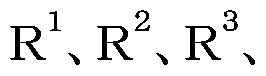 R6及び R7は、上記 一般式 (i)〜(iv)及び (vi)中の
 R2、 R3、 R6及び R7と同義である。ま た、
 R6及び R7は、複数存在する場合、それぞれ同一でも異 なっていてもよい。また、 mは 2〜500の整数を示し、 3〜20の整数であることが好ま しい。 nは 1〜500の整数を示し、 2〜20であることが好ましい。 pは 1〜500の整数を 示し、 1〜10であることが好ましい。これらの中で、 7 ヽ Z2及び Z3がすべて硫黄原子 であり、かつ R1がフッ素原子であるものが特に好ましい。
[0065] また、本発明の重合体の末端基として重合活性基を有して!/、る場合、それらは他の 重合体の前駆体として用いることもできる。その場合、本発明の重合体は分子内に 2 つの重合活性基を有していることが好ましい。重合活性基としては、ハロゲン原子、 アルキルスルホネート基、ァリールスルホネート基、ァリールアルキルスルホネート基 、アルキルスタ -ル基、ァリールスタ-ル基、ァリールアルキルスタ -ル基、ホウ酸ェ ステル基、スルホ -ゥムメチル基、ホスホ-ゥムメチル基、ホスホネートメチル基、モノ ハロゲン化メチル基、ホウ酸基、ホルミル基、又はビュル基が例示され、ハロゲン原子 、アルキルスタ -ル基、ホウ酸エステル基が好ましい。
[0066] また、本発明の重合体を有機薄膜として用いる場合、末端基に重合活性基がその まま残っていると、素子にしたときの特性や耐久性が低下する可能性があるので、安 定な基で保護するようにしてもょ ヽ。
[0067] 末端基としては、水素原子、アルキル基、アルコキシ基、フルォロアルキル基、フル ォロアルコキシ基、ァリール基、複素環基、電子供与基又は電子吸引基が挙げられ、 電子輸送性を高めると 、う観点からフルォロアルキル基、フルォロアルコキシ基又は 電子吸引基が好ましい。また、主鎖の共役構造と連続した共役結合を有しているもの も好ましぐ例えば、炭素 炭素結合を介してァリール基又は複素環基と結合してい
る構造が例示される。
[0068] 本発明の含フッ素重合体として、特に好ましいものとしては、例えば、下記一般式 (
68)〜(72)で表されるものが挙げられる。
[0069] [化 19]

[0072] [化 22]


[0074] ここで、上記一般式 (68)〜(72)中、 R11及び 末端基を示し、同一でも異なつ ていても良ぐ先に例示した末端基が挙げられ、フルォロアルキル基であることが好ま しい。また、 R13、 R"、 R15及び R16はそれぞれ独立に、水素原子又は任意の置換基 を示し、アルキル基又はアルコキシ基であることが好ましぐアルキル基であることがよ り好ましい。重合体中に R13、 R14、 R15及び R16が複数存在する場合、それらは同一で あっても異なっていてもよい。なお、製造上の容易さからは、複数存在する R13、 R14、 R15及び R16は同一であることが好ましい。また、 R2、 R3、 u2及び v2は、上記一般式 (I )及び (IV)中の 、 R3、 u2及び v2と同義である。
[0075] 更に、 q及び rは、重合体を用いた有機薄膜の形成方法に応じて適宜選ぶことがで きる。真空蒸着法等の気相成長法を用いて有機薄膜を形成する場合、重合体はオリ ゴマーであることが好ましぐ qは 2〜 10の整数であることが好ましぐ 3〜 10の整数で あることがより好ましぐ 3〜5の整数であることが更に好ましぐ rは 1〜10の整数であ ることが好ましぐ 2〜 10の整数であることがより好ましぐ 2〜5の整数であることが更 に好ましい。一方、重合体を有機溶剤に溶解した溶液を塗布する方法を用いて有機 薄膜を形成する場合、 q及び rは 3〜500の整数であることが好ましぐ 6〜300の整 数であることがより好ましぐ 20〜200の整数であることが更に好ましい。また、塗布
法で成膜したときの膜の均一性の観点から、重合体のポリスチレン換算の数平均分 子量は、 1 X 10³〜1 X 10⁸であることが好ましぐ 1 X 10⁴〜1 X 10⁶であることがより好 ましい。
[0076] 本発明の含フッ素化合物又はそれから誘導される含フッ素重合体の製造方法は特 に限定されず、どのような方法により製造してもよいが、以下に説明する製造方法に より製造することが好ましい。
[0077] 上記一般式 (I)で表される本発明の含フッ素化合物は、前駆体として下記一般式( VII)で表される化合物又は下記一般式 (Vila)で表される化合物を用い、この前駆 体をフッ素化剤と反応させるフッ素化工程を含む製造方法により製造することが可能 である。すなわち、上記一般式 (I)で表される化合物は、下記一般式 (Vila)で表され る化合物を前駆体として用い、例えば、アルコールをフッ素化させる Organic Reactions vol.35, p.315 (1988)し nap.3 Fluonnationwith
DAST〃に記載された方法と同様にして、上記前駆体をフッ素化剤と反応させる工程 を含む製造方法により製造することが可能である。この反応工程の一例として、下記 反応式 (a)に示した化合物(73)から化合物(74)への変換工程が挙げられる。
[0078] [化 24]

[式 (Vila)中、 Ar1及び Ar2は各々独立に、炭素数 10以上の芳香族炭化水素基又 は炭素数 4以上の複素環基を示し、 R2及び R3は各々独立に、 1価の置換基を示し、 Vは水酸基又は 1価の置換基を示し、 si及び tlは各々独立に、 0以上の整数を示す 。但し、 siが 2以上の場合、複数存在する R2は同一でも異なっていてもよぐ tlが 2以 上の場合、複数存在する R3は同一でも異なっていてもよい。 ]
[0079] [化 25]

(73)
[0080] また、上記一般式 (I)で表される本発明の化合物のうち、 R1がフッ素原子であるィ匕 合物は、下記一般式 (VII)で表される化合物を前駆体として用い、この前駆体を、ハ ロニゥムイオン発生剤の存在下、フッ化物イオン源と反応させる工程を含む製造方法 により製造することが好ましい。この反応工程の一例として、下記反応式 (b)に示した 化合物(75)から化合物(76)への変換工程が挙げられる。
[0081] [化 26]

[式 (VII)中、 Ar1及び Ar2は各々独立に、炭素数 10以上の芳香族炭化水素基又は 炭素数 4以上の複素環基を示し、 R2及び R3は各々独立に、 1価の置換基を示し、 X 及び Yは、各々独立にアルキルチオ基を示す力 或いは、 X及び Yのアルキルチオ 基のアルキル部分が連結してなるアルキレンジチォ基、又は、 X及び Yがー体となつ て、結合する炭素原子とともに形成するチォカルボ-ル基を示し、 si及び tlは各々 独立に、 0以上の整数を示す。但し、 siが 2以上の場合、複数存在する R2は同一で も異なっていてもよぐ tlが 2以上の場合、複数存在する R3は同一でも異なっていて ちょい。]
[0082] [化 27]

(76)
[0083] 上記一般式 (VII)で表される化合物を前駆体として用いた上記反応工程における 反応条件は特に限定されず、例えば、アルキルスルファ-ル基 (アルキルチオ基)等 力もフルォロ基への公知の変換反応における条件 (例えば、特開平 6— 135869号 公報等参照)を参考にして適宜選択してもよい。以下、具体的に説明する。
[0084] まず、上記フッ化物イオン源としては、例えば、フッ化水素、フッ化水素とァミンとの 錯体、フッ化水素とピリジンとの錯体、二水素三フッ化四級アンモ-ゥム、又は二水素 三フッ化四級ホスホ-ゥムが好ましぐこれらは単独で用いても 2種類以上を併用して もよい。最適なフッ化物イオン源としては、例えば、(フッ化水素) 9 Ζピリジン錯体が挙 げられる。
[0085] なお、上記ァミンとしては、例えば、ピリジン等の含窒素環式ィ匕合物、トリェチルアミ ン、ジイソプロピルェチルァミン等のアルキルアミン等が挙げられる。また、二水素三 フツイ匕四級アンモ-ゥム及び二水素三フッ化四級ホスホ-ゥムは特に限定されず、公 知の化合物を適宜用いることができる。二水素三フッ化四級アンモ-ゥムとしては、 例えば下記一般式 (XI)で表される化合物が挙げられ、二水素三フッ化四級ホスホニ ゥムとしては、例えば下記一般式 (ΧΠ)で表される化合物が挙げられる。
R20R21R22R23N + H ρ - . . . (¾)
R24R25R26R27P+H F _ … (XII)
2 3
[0086] 上記一般式 (XI)及び (ΧΠ)中、 R2°、 R21、 R22、 R23、
 R26及び R27はそれ ぞれ独立に、アルキル基、ァリール基、ベンジル基等の炭化水素基を示す。上記一 般式 (XI)で表される二水素三フツイ匕四級アンモ-ゥムとしては、例えば、二水素三フ ッ化テトラメチルアンモ-ゥム、二水素三フッ化テトラェチルアンモ-ゥム、二水素三 フッ化テトラブチルアンモ -ゥム(TBAH F )、二水素三フッ化ベンジルトリメチルァ
2 3
ンモ-ゥム、二水素三フッ化べンジルトリェチルアンモ-ゥム、二水素三フッ化セチル トリメチルアンモ -ゥム等が挙げられる。これらは、例えば、 50%フッ酸、フッ化力リウ ム及びフッ化四級アンモ-ゥム力 容易に合成できる(例えば、 Bull.
Soc. Chim. Fr., 910 (1986)等参照)。また、上記一般式 (ΧΠ)で表される二水素三フ ッ化四級ホスホ-ゥムとしては、例えば、二水素三フッ化テトラメチルホスホ-ゥム、二 水素三フッ化テトラェチルホスホ-ゥム、二水素三フッ化テトラブチルホスホ-ゥム、 二水素三フッ化べンジルトリメチルホスホ-ゥム、二水素三フッ化べンジルトリェチル ホスホ-ゥム、二水素三フッ化セチルトリメチルホスホ-ゥム等が挙げられる。
[0087] 上記反応工程における上記フッ化物イオン源の使用量は、特に限定されないが、 例えば、フッ化物イオン換算で 3当量〜大過剰量の範囲であり、反応効率及びコスト の観点から、例えば 3〜5当量が好ましい。
[0088] また、上記反応工程における上記ハロニゥムイオン発生剤としては、特に限定され ず、公知のものを適宜用いることができ、例えば、 1, 3—ジブロモ— 5, 5—ジメチルヒ ダントイン(DBH)ゝ N—ブロモコハク酸イミド(NBS)、 N—ブロモアセトアミド(NBA) 、 2, 4, 4, 6—テトラブロモー 2, 5—シクロへキサジェノン、 N—ョードコハク酸イミド( NIS)等が挙げられる。上記ハ口-ゥムイオン発生剤の使用量は、特に限定されない 力 例えば、ハロニゥムイオン換算で 3当量〜大過剰量の範囲であり、反応効率及び コストの観点から、例えば 3〜5当量が好ましい。
[0089] また、上記反応工程にお!、て、必要に応じて溶媒を適宜用いてもよ!、。上記溶媒 は特に限定されないが、なるべく目的の反応を阻害しないものであることが好ましぐ 例えば、へキサン等の脂肪族炭化水素、ベンゼン、トルエン等の芳香族炭化水素、 ァセトニトリル等の二トリル、ジェチルエーテル、テトラヒドロフラン、 1, 2—ジメトキシェ タン等のエーテル、ジクロロメタン、 1, 2—ジクロ口エタン、四塩化炭素等のハロゲン 化溶媒等が挙げられる。これらは、単独で用いても良いし 2種類以上併用してもよい 。最適な溶媒としては、例えばジクロロメタンが挙げられる。
[0090] また、上記反応工程における反応温度及び反応時間は特に限定されず、前駆体 の種類を考慮して適宜選択することができる。なお、上記反応温度は、例えば、 - 10 0°C〜100°Cの範囲である。
[0091] 上記本発明の製造方法により、従来は不可能であった、フルォロアルキルで架橋し た環状ィ匕合物、特にジフルォロアルキルで架橋したビチォフェン構造を含む化合物 を、簡便に且つ高収率で製造できるようになった。また、本発明の製造工程における フッ素化反応では、安価で取り扱いが容易なフッ素化試薬を用いてフッ素化を行うこ とちでさる。
[0092] 本発明の含フッ素化合物を有機薄膜素子用の材料として用いる場合、その純度が 素子特性に影響を与えるため、製造した化合物を蒸留、昇華精製、再結晶等の方法 で純化処理することが好ま ヽ。
[0093] 以上、本発明の含フッ素化合物の製造方法について説明した力 本発明の製造方 法における反応条件、反応試薬等は、上記の例示以外にも適宜選択可能である。ま た、上記一般式 (I)で表される本発明の含フッ素化合物は、上述の通り、本発明の製 造方法により製造することが好ましいが、これに限定されず、どのような方法により製 造してちょい。
[0094] 次に、本発明の含フッ素重合体の製造方法について説明する。本発明の含フッ素 重合体は、例えば、下記一般式 (ΧΠΙ)〜 (XVI)で表される化合物を原料として、こ れらを反応させること〖こより製造することができる。
[0095] [化 28]

■■■ (XIV)
 [0097] [化 30]
W1― Ar3— W2 ■■■ (XV) [0098] [化 31]

[0099] 上記一般式 (XIII)〜 (XVI)中、 ΑΛ Ar2、 Ar3、

s2、 t2、 u2及び v2は、上記一般式(I)〜(VI)中の ΑΛ Ar2、 Ar3、 z z z R R2、 R3、 R6、 R7、 s2、 t2、 u2及び v2と同義である。また、 W1及び W2はそれぞれ独立 に、ハロゲン原子、アルキルスルホネート基、ァリールスルホネート基、ァリールアル キルスルホネート基、アルキルスタ -ル基、ァリールスタ-ル基、ァリールアルキルス タニル基、ホウ酸エステル基、スルホ -ゥムメチル基、ホスホ-ゥムメチル基、ホスホネ 一トメチル基、モノハロゲン化メチル基、ホウ酸基、ホルミル基、又はビニル基を示す
[0100] 上記一般式 (ΧΙΠ)〜 (XVI)で表される化合物の合成上の反応のしゃすさの観点 から、 w1及び w2はそれぞれ独立に、ハロゲン原子、アルキルスルホネート基、ァリー ルスルホネート基、ァリールアルキルスルホネート基、アルキルスタ -ル基、ホウ酸ェ ステル基又はホウ酸基であることが好ま U、。
[0101] また、本発明の重合体の製造に用いる反応方法としては、例えば、 Wittig反応を 用いる方法、 Heck反応を用いる方法、 Horner—Wadsworth—Emmons反応を用 いる方法、 Knoevenagel反応を用いる方法、 Suzukiカップリング反応を用いる方法 、 Grignard反応を用いる方法、 Stille反応を用いる方法、 Ni(0)触媒を用いる方法 等が例示される。また、重合体は、重合性官能基による反応以外によって形成されて いてもよい。例えば、一般式 (I)において、 sl、 tlが 0である縮合環化合物同士を、 F eClを用いた酸化重合反応や電気化学的な酸化による重合反応等によって繰り返
し重合させる方法も例示される。
[0102] これらのうち、 Wittig反応を用いる方法、 Heck反応を用いる方法、 Horner— Wad sworth— Emmons反応を用 ヽる方法、 Knoevenagel反応を用 ヽる方法、 Suzuki カップリング反応を用いる方法、 Grignard反応を用いる方法、 Stille反応を用いる方 法、及び Ni (0)触媒により重合する方法が、構造制御がしやすいので好ましい。さら に、 Suzukiカップリング反応を用いる方法、 Grignard反応を用いる方法、 Stille反 応を用いる方法、 Ni(0)触媒を用いる方法が、原料の入手しやすさと反応操作の簡 便さから好ましい。
[0103] モノマー(上記一般式 (ΧΙΠ)〜 (XVI)で表される化合物)は、必要に応じ、有機溶 媒に溶解し、例えばアルカリや適当な触媒を用い、有機溶媒の融点以上沸点以下で 、反応させることができる。
[0104] 有機溶媒としては、用いる化合物や反応によっても異なるが、一般に副反応を抑制 するために、十分に脱酸素処理を施したものを用い、不活性雰囲気下で反応を進行 させることが好ましい。また、同様に、脱水処理を行うことが好ましい(但し、 Suzuki力 ップリング反応のような水との 2相系での反応の場合にはその限りではない)。
[0105] 本発明の重合体を製造する際、上記一般式 (XIII)〜 (XVI)で表される化合物を反 応させるために、適宜アルカリや適当な触媒を添加することができる。これらは用いる 反応に応じて選択すればよい。また、上記アルカリ又は触媒は、反応に用いる溶媒 に十分に溶解するものを使用することが好まし 、。
[0106] 本発明の重合体を有機薄膜素子用の材料として用いる場合、その純度が素子特 性に影響を与えるため、反応前のモノマーを蒸留、昇華精製、再結晶等の方法で精 製したのちに重合することが好ましぐまた合成後、再沈精製、クロマトグラフィーによ る分別等の純ィ匕処理をすることが好まし 、。
[0107] 反応に用いられる溶媒としては、ペンタン、へキサン、ヘプタン、オクタン、シクロへ キサン等の飽和炭化水素、ベンゼン、トルエン、ェチルベンゼン、キシレン等の不飽 和炭化水素、四塩化炭素、クロ口ホルム、ジクロロメタン、クロロブタン、ブロモブタン、 クロ口ペンタン、プロモペンタン、クロ口へキサン、ブロモへキサン、クロロシクロへキサ ン、ブロモシクロへキサン等のハロゲン化飽和炭化水素、クロ口ベンゼン、ジクロロべ
ンゼン、トリクロ口ベンゼン等のハロゲン化不飽和炭化水素、メタノール、エタノール、 プロパノール、イソプロパノール、ブタノール、 t ブチルアルコール等のアルコール 類、蟻酸、酢酸、プロピオン酸等のカルボン酸類、ジメチルエーテル、ジェチルエー テル、メチルー t ブチルエーテル、テトラヒドロフラン、テトラヒドロピラン、ジォキサン 等のエーテル類、塩酸、臭素酸、フッ化水素酸、硫酸、硝酸等の無機酸等が例示さ れ、単一溶媒、又はこれらの混合溶媒を用いてもよい。
[0108] 反応後は、例えば水でタエンチした後に有機溶媒で抽出し、溶媒を留去する等の 通常の後処理で生成物を得ることができる。生成物の単離後及び精製は、クロマトグ ラフィ一による分取や再結晶等の方法により行うことができる。
[0109] 次に、本発明の有機薄膜について説明する。本発明の有機薄膜は、上記本発明 の含フッ素化合物及び Z又は含フッ素重合体を含有することを特徴とする。
[0110] 本発明の有機薄膜の膜厚としては、通常 Inn!〜 100 m程度であり、好ましくは 2 ηπ!〜 lOOOnmであり、さらに好ましくは 5nm〜500nmであり、特に好ましいのは 20 nm〜200nmである。
[0111] 有機薄膜は、上記化合物及び上記重合体のうちの 1種類を単独で含むものであつ てもよぐ上記化合物及び上記重合体のうちの 2種類以上を含むものであってもよい 。また、有機薄膜の電子輸送性又はホール輸送性を高めるため、上記化合物又は上 記重合体以外に、電子輸送性又はホール輸送性を有する低分子化合物又は重合 体を混合して用いることもできる。
[0112] ホール輸送性材料としては、公知のものが使用でき、例えば、ピラゾリン誘導体、ァ リールァミン誘導体、スチルベン誘導体、トリフエ-ルジァミン誘導体、オリゴチォフエ ン若しくはその誘導体、ポリビュル力ルバゾール若しくはその誘導体、ポリシラン若し くはその誘導体、側鎖若しくは主鎖に芳香族ァミンを有するポリシロキサン誘導体、 ポリア-リン若しくはその誘導体、ポリチォフェン若しくはその誘導体、ポリピロール若 しくはその誘導体、ポリフエ-レンビ-レン若しくはその誘導体、又はポリチェ-レンビ 二レン若しくはその誘導体等が例示される。また、電子輸送性材料としては、公知の ものが使用でき、例えば、ォキサジァゾール誘導体、アントラキノジメタン若しくはその 誘導体、ベンゾキノン若しくはその誘導体、ナフトキノン若しくはその誘導体、アントラ
キノン若しくはその誘導体、テトラシァノアンスラキノジメタン若しくはその誘導体、フ ルォレノン誘導体、ジフエ-ルジシァノエチレン若しくはその誘導体、ジフエノキノン 誘導体、又は 8—ヒドロキシキノリン若しくはその誘導体の金属錯体、ポリキノリン若し くはその誘導体、ポリキノキサリン若しくはその誘導体、ポリフルオレン若しくはその誘 導体、 C 等のフラーレン類及びその誘導体等が例示される。
60
[0113] また、本発明の有機薄膜は、有機薄膜中で吸収した光により電荷を発生させるため に、電荷発生材料を含んでいてもよい。電荷発生材料としては公知のものが使用で き、ァゾ化合物及びその誘導体、ジァゾ化合物及びその誘導体、無金属フタロシア ニン化合物及びその誘導体、金属フタロシアニン化合物及びその誘導体、ペリレン 化合物及びその誘導体、多環キノン系化合物及びその誘導体、スクァリリウム化合物 及びその誘導体、ァズレニウム化合物及びその誘導体、チアピリリウム化合物及びそ の誘導体、 C 等のフラーレン類及びその誘導体等が例示される。
60
[0114] さらに、本発明の有機薄膜は、種々の機能を発現させるために必要な材料を含ん でいてもよい。例えば、吸収した光により電荷を発生させる機能を増感するための増 感剤、安定性を増すための安定化剤、 UV光を吸収するための UV吸収剤等が例示 される。
[0115] また、本発明の有機薄膜は、機械的特性を高めるため、上記化合物又は上記重合 体以外の高分子化合物材料を高分子バインダーとして含んで!/、てもよ!/、。高分子バ インダ一としては、電子輸送性又はホール輸送性を極度に阻害しな 、ものが好ましく 、また可視光に対する吸収が強くないものが好ましく用いられる。
[0116] このような高分子バインダーとしては、ポリ(N—ビュルカルバゾール)、ポリア-リン 若しくはその誘導体、ポリチォフェン若しくはその誘導体、ポリ(p—フエ-レンビ-レ ン)若しくはその誘導体、ポリ(2, 5—チェ-レンビ-レン)若しくはその誘導体、ポリ カーボネート、ポリアタリレート、ポリメチルアタリレート、ポリメチルメタタリレート、ポリス チレン、ポリ塩化ビュル、ポリシロキサン等が例示される。
[0117] 本発明の有機薄膜の製造方法としては、特に制限はないが、例えば、上記化合物 及び Z又は上記重合体、必要に応じて混合する電子輸送性材料又はホール輸送性 材料、高分子ノ インダ一等を含む溶液を用いて成膜する方法が例示される。また、
本発明の化合物及び z又はこれを含むオリゴマーを用いる場合は、真空蒸着法によ り薄膜に形成することもできる。
[0118] 上記溶液を用いて成膜する際に使用する溶媒としては、上記化合物及び Z又は上 記重合体、並びに必要に応じて混合する電子輸送性材料又はホール輸送性材料、 高分子バインダー等を溶解させるものであれば特に制限されない。かかる溶媒として 具体的には、例えば、トルエン、キシレン、メシチレン、テトラリン、デカリン、 n—プチ ルベンゼン等の不飽和炭化水素系溶媒、四塩化炭素、クロ口ホルム、ジクロロメタン、 ジクロロエタン、クロロブタン、ブロモブタン、クロ口ペンタン、プロモペンタン、クロ口へ キサン、ブロモへキサン、クロロシクロへキサン、ブロモシクロへキサン等のハロゲンィ匕 飽和炭化水素系溶媒、クロ口ベンゼン、ジクロロベンゼン、トリクロ口ベンゼン等のハロ ゲンィ匕不飽和炭化水素系溶媒、テトラヒドロフラン、テトラヒドロピラン等のエーテル類 系溶媒等が例示される。上記化合物又は上記重合体の構造や分子量にもよるが、通 常はこれらの溶媒に 0. 1質量%以上溶解させることができる。
[0119] 上記溶液を用いた成膜方法としては、スピンコート法、キャスティング法、マイクログ ラビアコート法、グラビアコート法、バーコート法、ロールコート法、ワイア一バーコート 法、ディップコート法、スプレーコート法、スクリーン印刷法、フレキソ印刷法、オフセッ ト印刷法、インクジェット印刷法、ディスペンサー印刷法、ノズルコート法、キヤビラリ一 コート法等の塗布法を用いることができ、スピンコート法、フレキソ印刷法、インクジェ ット印刷法、ディスペンサー印刷法、ノズルコート法、キヤビラリ一コート法が好ましい
[0120] 本発明の有機薄膜を製造する工程には、上記化合物及び Z又は上記重合体を配 向させる工程が含まれて!、てもよ!、。この工程により上記化合物及び Z又は上記重 合体を配向させた有機薄膜は、主鎖分子又は側鎖分子が一方向に並ぶので、電子 移動度又はホール移動度が向上する。
[0121] 上記化合物及び Z又は上記重合体を配向させる方法としては、液晶の配向手法と して知られている方法を用いることができる。中でもラビング法、光配向法、シ アリン グ法 (ずり応力印加法)や引き上げ塗布法が配向手法として簡便かつ有用で利用し やすぐこれらの中でも、ラビング法、シェアリング法がより好ましい。
[0122] 本発明の有機薄膜は、電子輸送性又はホール輸送性を有することから、電極から 注入された電子又はホール、あるいは光吸収により発生した電荷を輸送制御すること により、有機薄膜トランジスタ、有機太陽電池、光センサ等、種々の有機薄膜素子に 用いることができる。本発明の有機薄膜をこれらの有機薄膜素子に用いる場合は、配 向処理により配向させて用いることが電子輸送性又はホール輸送性がより向上する ため好ましい。
[0123] 次に、本発明の有機薄膜の有機薄膜トランジスタへの応用について説明する。有 機薄膜トランジスタは、ソース電極及びドレイン電極、これらの間の電流経路となり本 発明の化合物及び Z又は上記重合体を含有する有機薄膜層 (活性層)、電流経路 を通る電流量を制御するゲート電極を備えた構造であればよぐ電界効果型、静電 誘導型等の有機薄膜トランジスタが例示される。
[0124] 電界効果型有機薄膜トランジスタは、ソース電極及びドレイン電極、これらの間の電 流経路となり本発明の化合物及び Z又は上記重合体を含む有機薄膜層 (活性層)、 電流経路を通る電流量を制御するゲート電極、並びに、活性層とゲート電極との間に 配置される絶縁層を備えることが好ましい。特に、ソース電極及びドレイン電極力 本 発明の化合物及び Z又は上記重合体を含む有機薄膜層 (活性層)に接して設けら れており、さらに有機薄膜層に接した絶縁層を挟んでゲート電極が設けられているこ とが好ましい。
[0125] 静電誘導型有機薄膜トランジスタは、ソース電極及びドレイン電極、これらの間の電 流経路となり本発明の化合物及び Z又は上記重合体を含有する有機薄膜層、並び に電流経路を通る電流量を制御するゲート電極を有し、該ゲート電極が有機薄膜層 中に設けられていることが好ましい。特に、ソース電極、ドレイン電極及び有機薄膜層 中に設けられたゲート電極が、本発明の化合物及び Z又は上記重合体を含有する 有機薄膜層に接して設けられていることが好ましい。ゲート電極の構造としては、ソー ス電極からドレイン電極へ流れる電流経路が形成され、かつゲート電極に印加した電 圧で電流経路を流れる電流量が制御できる構造であればよぐ例えば、くし形電極が 例示される。
[0126] 図 1は第 1実施形態に係る有機薄膜トランジスタ (電界効果型有機薄膜トランジスタ
)の模式断面図である。図 1に示す有機薄膜トランジスタ 100は、基板 1と、基板 1上 に所定の間隔を持って形成されたソース電極 5及びドレイン電極 6と、ソース電極 5及 びドレイン電極 6を覆うようにして基板 1上に形成された活性層 2と、活性層 2上に形 成された絶縁層 3と、ソース電極 5とドレイン電極 6との間の絶縁層 3の領域を覆うよう に絶縁層 3上に形成されたゲート電極 4と、を備えるものである。
[0127] 図 2は第 2実施形態に係る有機薄膜トランジスタ (電界効果型有機薄膜トランジスタ )の模式断面図である。図 2に示す有機薄膜トランジスタ 110は、基板 1と、基板 1上 に形成されたソース電極 5と、ソース電極 5を覆うようにして基板 1上に形成された活 性層 2と、ソース電極 5と所定の間隔を持って活性層 2上に形成されたドレイン電極 6 と、活性層 2及びドレイン電極 6上に形成された絶縁層 3と、ソース電極 5とドレイン電 極 6との間の絶縁層 3の領域を覆うように絶縁層 3上に形成されたゲート電極 4と、を 備えるものである。
[0128] 図 3は第 3実施形態に係る有機薄膜トランジスタ (電界効果型有機薄膜トランジスタ )の模式断面図である。図 3に示す有機薄膜トランジスタ 120は、基板 1と、基板 1上 に形成されたゲート電極 4と、ゲート電極 4を覆うようにして基板 1上に形成された絶縁 層 3と、ゲート電極 4が下部に形成されている絶縁層 3の領域を一部覆うように、絶縁 層 3上に所定の間隔を持って形成されたソース電極 5及びドレイン電極 6と、ソース電 極 5及びドレイン電極 6を覆うように絶縁層 3上に形成された活性層 2と、を備えるもの である。
[0129] 図 4は第 4実施形態に係る有機薄膜トランジスタ (電界効果型有機薄膜トランジスタ )の模式断面図である。図 4に示す有機薄膜トランジスタ 130は、基板 1と、基板 1上 に形成されたゲート電極 4と、ゲート電極 4を覆うようにして基板 1上に形成された絶縁 層 3と、ゲート電極 4が下部に形成されている絶縁層 3の領域を一部覆うように絶縁層 3上に形成されたソース電極 5と、ソース電極 5を覆うようにして絶縁層 3上に形成され た活性層 2と、ゲート電極 4が下部に形成されて!、る活性層 2の領域を一部覆ように、 ソース電極 5と所定の間隔を持って絶縁層 3上に形成されたドレイン電極 6と、を備え るものである。
[0130] 図 12は第 5実施形態に係る有機薄膜トランジスタ (電界効果型有機薄膜トランジス
タ)の模式断面図である。図 12に示す有機薄膜トランジスタ 140は、基板 1と、基板 1 上に形成された活性層 2と、活性層 2上に所定の間隔を持って形成されたソース電極 5及びドレイン電極 6と、ソース電極 5及びドレイン電極 6を覆うようにして活性層 2上に 形成された絶縁層 3と、ソース電極 5が下部に形成されている絶縁層 3の領域とドレイ ン電極 6が下部に形成されている絶縁層 3の領域とをそれぞれ一部覆うように、絶縁 層 3上に形成されたゲート電極 4と、を備えるものである。
[0131] 図 13は第 6実施形態に係る有機薄膜トランジスタ (電界効果型有機薄膜トランジス タ)の模式断面図である。図 13に示す有機薄膜トランジスタ 150は、基板 1と、基板 1 上に形成されたゲート電極 4と、ゲート電極 4を覆うようにして基板 1上に形成された絶 縁層 3と、ゲート電極 4が下部に形成されている絶縁層 3の領域を覆うように形成され た活性層 2と、ゲート電極 4が下部に形成されて!、る活性層 2の領域を一部覆うように 絶縁層 3上に形成されたソース電極 5と、ゲート電極 4が下部に形成されている活性 層 2の領域を一部覆うように、ソース電極 5と所定の間隔を持って絶縁層 3上に形成さ れたドレイン電極 6と、を備えるものである。
[0132] 図 14は第 7実施形態に係る有機薄膜トランジスタ (静電誘導型有機薄膜トランジス タ)の模式断面図である。図 14に示す有機薄膜トランジスタ 160は、基板 1と、基板 1 上に形成されたソース電極 5と、ソース電極 5上に形成された活性層 2と、活性層 2上 に所定の間隔を持って複数形成されたゲート電極 4と、ゲート電極 4の全てを覆うよう にして活性層 2上に形成された活性層 2a (活性層 2aを構成する材料は、活性層 2と 同一でも異なっていてもよい)と、活性層 2a上に形成されたドレイン電極 6と、を備え るものである。
[0133] 第 1〜第 7実施形態に係る有機薄膜トランジスタにおいては、活性層 2及び/又は 活性層 2aは、本発明の化合物及び Z又は上記重合体を含有しており、ソース電極 5 とドレイン電極 6の間の電流通路 (チャネル)となる。また、ゲート電極 4は、電圧を印 加することにより活性層 2及び Z又は活性層 2aにおける電流通路 (チャネル)を通る 電流量を制御する。
[0134] このような電界効果型有機薄膜トランジスタは、公知の方法、例えば特開平 5— 11 0069号公報記載の方法により製造することができる。また、静電誘導型有機薄膜トラ
ンジスタは、公知の方法、例えば特開 2004— 006476号公報記載の方法により製 造することができる。
[0135] 基板 1の材質としては有機薄膜トランジスタとしての特性を阻害しなければ特に制 限されな ヽが、ガラス基板やフレキシブルなフィルム基板やプラスチック基板も用いる ことができる。
[0136] 活性層 2を形成する際に、有機溶媒可溶性の化合物を用いることが製造上非常に 有利であり好ましいことから、上記で説明した本発明の有機薄膜の製造方法を用い て、活性層 2となる有機薄膜を形成することができる。
[0137] 活性層 2に接した絶縁層 3としては、電気の絶縁性が高い材料で有れば特に制限 はなぐ公知のものを用いることができる。例えば SiOx, SiNx、 Ta O、ポリイミ
2 5
ド、ポリビュルアルコール、ポリビュルフエノール、有機ガラス等が挙げられる。低電圧 化の観点から、誘電率の高!、材料の方が好ま 、。
[0138] 絶縁層 3の上に活性層 2を形成する場合は、絶縁層 3と活性層 2との界面特性を改 善するため、シランカップリング剤等の表面処理剤で絶縁層 3表面を処理して表面改 質した後に活性層 2を形成することも可能である。表面処理剤としては、長鎖アルキ ルクロロシラン類、長鎖アルキルアルコキシシラン類、フッ素化アルキルクロロシラン 類、フッ素化アルキルアルコキシシラン類、へキサメチルジシラザン等のシリルアミン 化合物等が挙げられる。表面処理剤で処理する前に、絶縁層表面をオゾン UV、 O
2 プラズマで処理をしておくことも可能である。
[0139] 有機薄膜トランジスタを作製後、素子を保護するために有機薄膜トランジスタ上に 保護膜を形成することが好ましい。これにより、有機薄膜トランジスタが大気力も遮断 され、有機薄膜トランジスタの特性の低下を抑えることができる。また、保護膜により、 有機薄膜トランジスタの上に駆動する表示デバイスを形成するときの影響を低減する ことができる。
[0140] 保護膜を形成する方法としては、 UV硬化榭脂、熱硬化榭脂ゃ無機の SiONx膜等 でカバーする方法等が挙げられる。保護膜を形成する際には、有機薄膜トランジスタ と大気との遮断を効果的に行うために、有機薄膜トランジスタの作製後、保護膜を形 成するまでの工程を大気に曝すことなく(例えば、乾燥した窒素雰囲気中、真空中等
で)行うことが好ましい。
[0141] 次に、本発明の有機薄膜の太陽電池への応用について説明する。図 5は、実施形 態に係る太陽電池の模式断面図である。図 5に示す太陽電池 200は、基板 1と、基 板 1上に形成された第 1の電極 7aと、第 1の電極 7a上に形成された本発明の化合物 及び Z又は本発明の重合体を含有する有機薄膜からなる活性層 2と、活性層 2上に 形成された第 2の電極 7bと、を備えるものである。
[0142] 本実施形態に係る太陽電池においては、第 1の電極 7a及び第 2の電極 7bの一方 に透明又は半透明の電極を用いる。電極材料としては、アルミニウム、金、銀、銅、ァ ルカリ金属、アルカリ土類金属等の金属又はそれらの半透明膜、透明導電膜を用い ることができる。高い開放電圧を得るためには、それぞれの電極は、仕事関数の差が 大きくなるように構成されることが好ましい。活性層 2 (有機薄膜)中には、光感度を高 めるために、キャリア発生剤、増感剤等を添加することができる。また、基板 1の材質 としては、シリコン基板、ガラス基板、プラスチック基板等を用いることができる。
[0143] 次に、本発明の有機薄膜の光センサへの応用を説明する。図 6は、第 1実施形態 に係る光センサの模式断面図である。図 6に示す光センサ 300は、基板 1と、基板 1 上に形成された第 1の電極 7aと、第 1の電極 7a上に形成された本発明の化合物及び Z又は本発明の重合体を含有する有機薄膜からなる活性層 2と、活性層 2上に形成 された電荷発生層 8と、電荷発生層 8上に形成された第 2の電極 7bと、を備えるもの である。
[0144] 図 7は、第 2実施形態に係る光センサの模式断面図である。図 7に示す光センサ 31 0は、基板 1と、基板 1上に形成された第 1の電極 7aと、第 1の電極 7a上に形成された 電荷発生層 8と、電荷発生層 8上に形成された本発明の化合物及び Z又は本発明 の重合体を含有する有機薄膜からなる活性層 2と、活性層 2上に形成された第 2の電 極 7bと、を備えるものである。
[0145] 図 8は、第 3実施形態に係る光センサの模式断面図である。図 8に示す光センサ 32 0は、基板 1と、基板 1上に形成された第 1の電極 7aと、第 1の電極 7a上に形成された 本発明の化合物及び Z又は本発明の重合体を含有する有機薄膜からなる活性層 2 と、活性層 2上に形成された第 2の電極 7bと、を備えるものである。
[0146] 第 1〜第 3実施形態に係る光センサにおいては、第 1の電極 7a及び第 2の電極 7b の一方に透明又は半透明の電極を用 ヽる。電荷発生層 8は光を吸収して電荷を発 生する層である。電極材料としては、アルミニウム、金、銀、銅、アルカリ金属、アル力 リ土類金属等の金属又はそれらの半透明膜、透明導電膜を用いることができる。活 性層 2 (有機薄膜)中には、光感度を高めるために、キャリア発生剤、増感剤等を添 加することができる。また、基板 1の材質としては、シリコン基板、ガラス基板、プラスチ ック基板等を用いることができる。
実施例
[0147] 以下、実施例及び比較例に基づいて本発明をさらに具体的に説明する力 本発明 は以下の実施例に何ら限定されるものではない。
[0148] (測定条件等)
核磁気共鳴 (NMR)スペクトルは、 JEOL (日本電子株式会社)製の商品名 JMN - 270 ( Η測定時 270MHz)、又は同社製の商品名 JMNLA—600 (19F測定時 600 MHz)を用いて測定した。ケミカルシフトは百万分率 (ppm)で表している。内部標準 Oppmには、テトラメチルシラン (TMS)を用いた。結合定数 (J)は、ヘルツで示してお り、略号 s、 d、 t、 q、 m及び brは、それぞれ、一重線(singlet)、二重線(doublet)、 三重線(triplet)、四重線(quartet)、多重線(multiplet)及び広幅線(broad)を表 す。また、質量分析 (MS)は、株式会社島津製作所製の GCMS— QP5050A (商品 名)を用い、電子イオン化 (EI)法、直接試料導入 (DI)法により測定した。カラムクロ マトグラフィー分離におけるシリカゲルは、関東ィ匕学株式会社製の商品名 Silicagel 60Ν (40〜50 /ζ πι)を用いた。全ての化学物質は、試薬級であり、和光純薬工業株 式会社、東京化成工業株式会社、関東ィ匕学株式会社、ナカライテスタ株式会社、シ ダマアルドリッチジャパン株式会社、又はダイキンィ匕成品株式会社より購入した。また 、サイクリックボルタンメトリーは、 BAS社製の装置を使用し、作用電極として BAS社 製 Pt電極、対電極として Pt線、参照電極として Ag線を用いて測定した。この測定時 の掃引速度は 100mVZsec、走査電位領域は 2. 8V〜1. 6Vであった。還元電 位及び酸化電位の測定は、化合物 1 X 10"3mol/L,及び、支持電解質としてのテト ラブチルアンモ -ゥムへキサフルオロフォスフェート(TBAPF6) 0. lmol/Lをモノフ
ルォロベンゼン溶媒に完全に溶解したものを用いて行った。また、 X線構造解析 (XR D)は、 Rigaku RAXIS -RAPID imaging plate diffractometerを用いて行 つた o
[0149] [参考合成例 1]
<化合物(78)の合成 >
出発原料である 4H シクロペンタ [2, 1— b : 3, 4— b,]ジチォフェンー4 オン( 化合物(77) )は、 Brzezinski,
J. Z.; Reynolds, J. R. Synthesis 2002, 8, 1053-1056.の記載を参照して合成した。こ の化合物(77)を用い、 Ong,B. S. Tetrahedron Lett. 1980,
21, 4225-4228.の記載を参照して、下記化合物(78)を合成した。すなわち、下記反 応式 (c)に従い、化合物(77)を出発原料として、これをジチオケタールイ匕することに より、化合物(78)を合成した。
[0150] [化 32]

[0151] [実施例 1]
<化合物 Aの合成 >
加熱乾燥した二つ口フラスコに N ブロモスクシンイミド(489mg、 2. 75mmol)を 入れて窒素置換した後、ジクロロメタン (4mL)をカ卩えた。この溶液を一 78°Cに冷却し 、フッ化水素 ピリジン(フッ化水素含有量 60〜70%、シグマアルドリッチジャパン社 より購入)(lmL)を滴下した。 78°Cで 30分撹拌した後、上記化合物(78) 105mg (0. 39mmol)のジクロロメタン溶液 (4mL)を滴下した。 78°Cで 3時間撹拌した後 、氷浴で 0°Cまで昇温し、さらに 1時間撹拌した。得られた反応液を 0°Cのへキサンで 希釈した後、ベーシックアルミナカラムを通した。次いで、減圧濃縮した後、シリカゲ ルカラムクロマトグラフィー (hexane)で精製を行!、、 目的物である黄色固体の化合
物 A (83mg、収率 57%)を得た。得られた化合物 Aの分析結果及び化学式は以下 の通りである。
TLし R = 0.6 (hexane: diethylether
f
= 3 : 1) : 1HNMR (270 MHz, CDC1 ): δ 7.10 (s, 2Η):
3
GC-MS (EI): m/z = 372 (M+).
[0152] [化 33]

[0153] [実施例 2]
<化合物 Bの合成 >
加熱乾燥したナスフラスコに化合物 A(446mg、 1. 20mmol)、テトラヒドロフラン(2 . 5mL)を入れた。次いで、窒素置換し、—78°Cに冷却した後、 n—ブチルリチウム( 1. 6M、 0. 81mL、 1. 3mmol)をカ卩えて反応させた。 1時間後、室温まで昇温させ た。次に、水を加え、酢酸ェチルで有機相を抽出した後、その有機相を硫酸マグネ シゥムで乾燥させた。次いで、減圧濃縮した後、シリカゲルカラムクロマトグラフィー (h exane)で精製を行!、、 目的物である緑色液体の化合物 B (246mg、収率 70%)を 得た。得られた化合物 Bの分析結果及びィ匕学式は以下の通りである。
TLC R = 0.6 (hexane): GC— MS (EI): m/z =
f
294 (M).
[0154] [化 34]
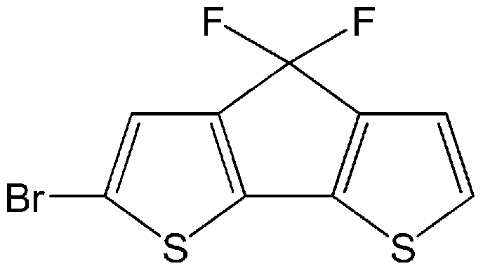
<化合物 Cの合成 >
加熱乾燥したナスフラスコに化合物 A (35 lmg、 0. 94mmol)、テトラヒドロフラン(1 OmL)を入れた。これを氷浴で 0°Cに冷却し、水素化リチウムアルミニウム(219mg、 5. 77mmol)を加えた後、室温で反応させた。 4時間後、水(220mg)、 2規定の水 酸ィ匕ナトリウム水溶液(220mg)、及び、水(660mg)をこの順に加えた。得られた混 合物を室温で撹拌した後、セライトろ過し、減圧濃縮した。その後、シリカゲルカラムク 口マトグラフィー (hexane)で精製することにより、 目的物である白色固体の化合物 C ( 191mg、収率 95%)を得た。得られた化合物 Cの分析結果及び化学式は以下の通 りである。また、得られたィ匕合物 Cについて、サイクリックボルタンメトリー(CV)法で測 定した酸化電位は 0. 99V、還元電位は— 2. 42Vであった。更に、得られた化合物 Cの吸収スペクトルのピーク波長は 359nmであった。
TLC R = 0.4 (hexane): ¾ NMR
f
(270 MHz, CDC1 ): δ 7.16 (d, 2H, J = 5.0 Hz), 7.08(d, 2H, J = 5.0
3
Hz): GC-MS (EI): m/z = 214 (M).
[0156] [化 35]

[実施例 4]
<化合物 Dの合成 >
加熱乾燥したナスフラスコに化合物 C (40mg、 0. 19mmol)、テトラヒドロフラン(2. OmL)を入れた。次いで、窒素置換し、—78°Cに冷却した後、 n—ブチルリチウム(1 . 6M、0. 13mL、0. 21mmol)をカ卩えて反応させた。 1時間後、— 78°Cで塩化トリブ チルスズ(100mg、 0. 307mmol)を加え、室温まで昇温させた。 12時間後、水をカロ え、ジクロロメタンで有機相を抽出した。この有機相を硫酸マグネシウム上で乾燥させ
、減圧濃縮した。その後、アルミナカラム (hexane)で精製を行い、 目的物である淡黄 色液体の化合物 D (70mg、収率 75%)を得た。得られた化合物 Dの分析結果及び 化学式は以下の通りである。
TLC R = 0.6 (hexane): GC— MS (DI): m/z =
f
504 (Μ .
[0158] [化 36]
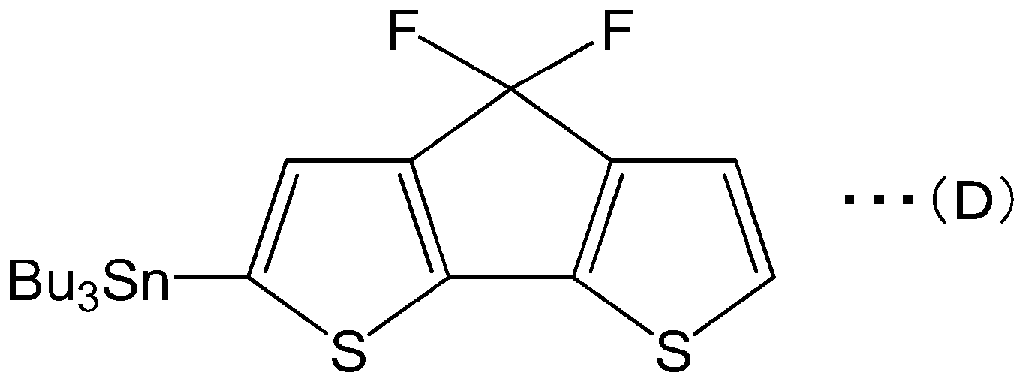
[0159] [実施例 5]
<化合物 Εの合成 >
加熱乾燥した蓋付き試験管に化合物八(12511^、0. 336mmol)、 2 トリブチルス タ-ルチオフェン(423mg、 1. 13mmol)、テトラキス(トリフエ-ルホスフィン)パラジ ゥム(0) (51mg、 0. 0441mmol)、及び、トルエン(3mL)を入れた後、窒素置換し、 120°Cで反応させた。 15時間後、放冷し、セライト濾過した後、減圧濃縮した。その 後、アルミナカラム (hexane)で精製を行!ヽ、 目的物である赤橙色固体の化合物 E (7 lmg、収率 56%)を得た。得られた化合物 Eの分析結果及びィ匕学式は以下の通りで ある。また、得られたィ匕合物 Eについて、 CV法で測定した酸ィ匕電位は 0. 57V、還元 電位は 2. 03Vであった。更に、得られた化合物 Eの吸収スペクトルのピーク波長 は 433nmであった。
TLC R = 0.2 (hexane): ¾
f
NMR(270 MHz, CDC1 ): δ 7.02 (dd, 2H, J =
3
5.0, 3.6 Hz), 7.16 (s, 2H), 7.18 (t, 2H, J = 3.6, 1.0 Hz), 7.25 (t, 2H, J = 5.0, 1.0 Hz): GC
-MS (EI): m/z = 378 (M+).
[0160] [化 37]
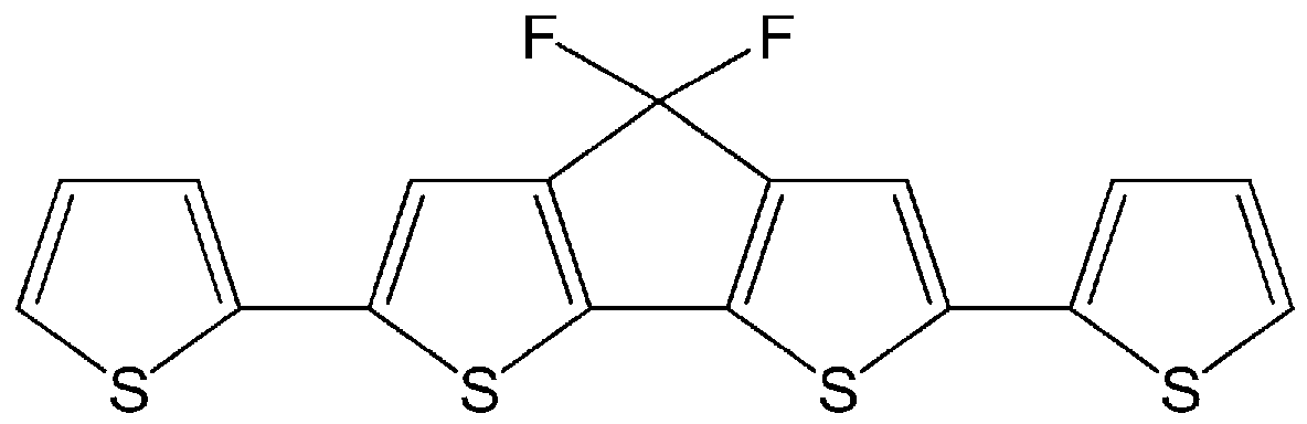
[0161] [実施例 6]
<化合物 Fの合成 >
加熱乾燥した蓋付き試験管に化合物八(13011^、0. 349mmol)、 2 トリブチルス タ-ル 5—パーフルォ口へキシルチオフェン(672mg、 0. 972mmol)、テトラキス( トリフエ-ルホスフィン)パラジウム(0) (40mg、 0. 0346mmol)、及び、トルエン(3m L)を入れた後、窒素置換し、 13時間還流させた。次いで、セライト濾過後、減圧濃縮 した。その後、アルミナカラム (hexane)で精製を行い、目的物である橙色固体の化 合物 F (131mg、収率 38%)を得た。得られた化合物 Fの分析結果及び化学式は以 下の通りである。また、得られた化合物 Fについて、 CV法で測定した酸ィ匕電位は 0. 88V、還元電位は 1. 95Vであった。更に、得られた化合物 Fの吸収スペクトルの ピーク波長は 433nmであった。
TLC R = 0.5 (hexane): ¾ NMR
f
(270 MHz'acetone- d ): δ 7.66 (s, 2Η), 7.65 (d, 2H, J = 4.3 Hz), 7.54
6
(d, 2H,J = 4.3 Hz): MS (MALDI— TOF, 1,8,9— trihydroxyanthracene matrix) m/z = 1018.5 (M+,Calcd 1014.6).
[0162] [化 38]

<X線構造解析 >
得られたィ匕合物 Fについて X線構造解析を行い、隣り合うチォフェン環同士の二面 角を測定したところ、中央のビチォフェン部分のチォフェン環同士のなす二面角は約
6度、中央のビチォフェン部分のチォフェン環と両端のチォフェン環とのなす二面角 は約 8度と、ほぼ平面であった(図 10参照)。また、結晶中で、化合物 Fは均一なスタ ック構造をとつて 、ることが確認された(図 11参照)。
[0164] [実施例 7]
<重合体 Gの合成 >
加熱乾燥した蓋付き試験管に化合物 B (26mg、 0. 089mmol)、化合物 C (70mg 、 0. 14mmol)、テトラキス(トリフエ-ルホスフィン)パラジウム(0) (25mg、 0. 022m mol)、及び、トルエン(1. 8mL)を入れた後、窒素置換し、 120°Cで反応させた。 14 時間後、放冷し、セライト濾過した後、減圧濃縮した。その後、アルミナカラム (hexan e)で精製し、目的物である黄橙色固体の重合体 G (15mg、収率 40%)を得た。得ら れた重合体 Gの分析結果及びィ匕学式は以下の通りである。また、得られた重合体 G について、 CV法で測定した酸化電位は 0. 66V、還元電位は— 2. 08Vであった。 更に、得られた重合体 Gの吸収スペクトルのピーク波長は 435nmであった。
TLC R = 0.4 (hexane: CH C1 =
f 2 2
4 :1): JH NMR(270 MHz, CDC1 ): δ 7.22 (d, 2H, J = 4.9
3
Hz), 7.15(s, 2H), 7.11 (d, 2H, J = 4.9 Hz): GC- MS (DI): m/z = 426 (M+).
[0165] [化 39]

[実施例 8]
<重合体 Hの合成 >
加熱乾燥した蓋付き試験管に化合物 A(172mg、 0. 462mmol)、化合物 D (516 mg、 1. O3mmol)、テトラキス(トリフエ-ルホスフィン)パラジウム(0) (73mg、 0. 06 3mmol)、及び、トルエン(lOmL)を入れた後、窒素置換し、 120°Cで反応させた。 1 0時間後、放冷し、析出した固体を濾取した後、その固体をアセトン、へキサン、及び
メタノールで洗浄した。その後、昇華精製し、目的物である茶色固体の重合体 H (95 mg、 42%)を得た。得られた重合体 Hの分析結果及びィ匕学式は以下の通りである。 また、得られた重合体 Hの吸収スペクトルのピーク波長は 488nmであった。
GC-MS (DI): m/z = 638 (M
[0167] [化 40]

[0168] [実施例 9]
<重合体 Jの合成 >
窒素置換した 50mlシュレンク型フラスコに、 2, 7—ビス(トリメチルスタ-ル)一9, 9 ージォクチルフルオレン(0. 13mmol)、化合物 A(0. l lmmol)、及び、ジクロロビ ス(トリフエ-ルホスフィン)パラジウム(0. 97 μ mol)を入れ、 DMF (ジメチルホルムァ ミド)を 3ml加えて 150°Cまで昇温し、 24時間撹拌した。続いて、 THF (テトラヒドロフ ラン)を 2ml加え、さらに 48時間撹拌した。次いで、室温まで冷却した後、メタノールと 水とを質量比 1: 1で混合した混合液 50mlで再沈殿させることにより、目的物である茶 色固体の重合体 J (50mg、 77%)を得た。得られた重合体 Jのポリスチレン換算の数 平均分子量は 4. 4 X 10³であった。また、得られた重合体 Jの化学式は以下の通りで ある。得られた重合体 Jは、薄膜状にした際の吸収スペクトルのピーク波長が 364nm であった。
[0169] [化 41]

[0170] [比較例 1]
<化合物 Kの合成 >
加熱乾燥した蓋付き試験管に化合物(77) (96mg、 0. 499mmol)、ヒドラジン一 水和物(268mg、 5. 35mmol)、水酸ィ匕カリウム(294mg、 5. 249mmol)、エチレン グリコール(5mL)を入れた後、室温から 190°Cまで徐々に加熱した後、 190°Cで 13 時間還流させた。次いで室温まで冷却した後、水を加え、エーテルで有機相を抽出 した。この有機相を水及び飽和食塩水で洗い、硫酸マグネシウム上で乾燥させ、減 圧濃縮した。その後、シリカゲルカラムクロマトグラフィー(hexane : ethyl acetate = 10 : 1)で精製することにより、目的物である白色固体の化合物 K (59mg、収率 66% )を得た。得られた化合物 Kの分析結果及びィ匕学式は以下の通りである。また、得ら れた化合物 Kについて、 CV法で測定した酸化電位は 0. 68V、還元電位は 2. 88 Vであった。更に、得られた化合物 Kの吸収スペクトルのピーク波長は 310nmであつ た。
TLC R = 0.7 (hexane: CH C1 =
f 2 2
2 :1): JH NMR (270 MHz, CDC1 ): δ 7.17 (d, 2Η, J = 4.8
3
Hz), 7.09 (d, 2H, J = 4.8 Hz), 3.54 (s, 2H): GC- MS (EI): m/z = 178 (M+).
[化 42]

[実施例 10]
<有機薄膜素子 1の作製及びトランジスタ特性の評価 >
ゲート電極となる高濃度にドープされた n—型シリコン基板の表面上に、熱酸ィ匕によ り絶縁層となるシリコン酸ィ匕膜を 300nm形成した基板を用意した。この基板を、 Aldri ch社製の Hexamethyldisilazane (HMDS)に 50°Cで 7時間浸漬し、シリコン酸化膜表 面を処理した。次に、この表面処理した基板上に、真空蒸着法により、基板温度 90 °C、堆積速度 2. OAZsecの条件で、化合物 Fの有機薄膜を 15nmの膜厚で堆積さ
せた。この有機薄膜の上に、シャドウマスクを通して Auを 30nmの厚さで蒸着し、チヤ ネル幅 5. 5mm、チャネル長 100 mのソース電極及びドレイン電極を形成して、有 機薄膜素子 1を作製した。得られた有機薄膜素子 1について、真空中でゲート電圧 V 、ソース一ドレイン間電圧 V を変化させてトランジスタ特性を測定したところ、良好
G SD
な Id— Vg特性が得られ、 Vg= 100V、 (1= 100¥にぉぃてドレィン電流1(1= 7. 3 X 10_6Aの電流が流れた。また、このときの移動度は 1. 8 X 10_2cm2ZVsであり、電 流がオンするしきい値電圧は Vth=64Vであった。このこと力 、化合物 Fを用いた 有機薄膜素子 1は、 n型有機トランジスタとして有効に機能することが確認された。
[0173] [実施例 11]
<有機薄膜素子 2の作製及び有機薄膜トランジスタ特性の評価 >
重合体 Jを 0. 008g秤量し、ジクロロベンゼンを加えて 2gとし、塗布液を調製する。 上記実施例 10と同様にして、表面処理した電極付き基板上に、上記の重合体 Jの塗 布液をスピンコート法により塗布する。これにより、基板上に重合体 Jを含む有機薄膜 を膜厚 700nmで形成し、有機薄膜素子 2を作製する。得られる有機薄膜素子 2は、 真空中でゲート電圧 V、ソース ドレイン間電圧 V を変化させてトランジスタ特性を
G SD
測定することにより良好な Isd—Vg特性が得られ、 n型有機トランジスタとして有効に 機能する。
[0174] [参考合成例 2]
<化合物(80)の合成 >
出発原料である 2, 2 ジー(3—チェ-ル)ー1, 3 ジォキソラン (ィ匕合物(79) )は 、 Lucas, P.; El Mehdi,
N.; Ho, H. A.; Belanger, D.; Breau,し Synthesis 2000, 9, 1253- 1258.の記載を参照 して合成した。この化合物(79)を用い、 Zotti, G.; Zecchin, S.; Schiavon, G.; Vercelli , B. Chem.
Mater.2004, 16, 3667-3676.の記載を参照して、下記化合物(80)を合成した。すな わち、下記反応式 (d)に従い、化合物(79)を出発原料として、これをモノブロモ化す ることにより、化合物(80)を合成した。
[0175] [化 43]

(79) (80)
[0176] <化合物 Lの合成 >
加熱乾燥した蓋付き試験管に化合物(80) (600mg、 1. 90mmol)、銅粉末(777 mg、 12. 2mmol)、ヨウ化パーフルォ口へキサン(1. l lg、 2. 48mmol)、及び、ジメ チルスルホキシド(20mL)を入れた後、窒素置換し、 115°Cで反応させた。 12時間 後、放冷し、水を加えてセライト濾過した。その後、酢酸ェチルで有機相を抽出し、こ の有機相を水で洗い、減圧濃縮した。次いで、減圧濃縮した有機相をテトラヒドロフラ ン(15mL)に溶かし、 12規定の塩酸 (4mL)をカ卩えて室温で反応させた。 10時間後 、水を加えて酢酸ェチルで有機相を抽出し、この有機相を水で洗い、硫酸マグネシ ゥム上で乾燥させ、減圧濃縮した。その後、シリカゲルカラムクロマトグラフィー (hexa ne)で精製を行!、、 目的物である赤色固体の化合物 L (264mg、収率 37%)を得た。 得られたィ匕合物 Lの分析結果及びィ匕学式は以下の通りである。
TLC R = 0.1 (hexane): JH
f
NMR(270 MHz, CDC1 ): δ 7.33 (s, 1H), 7.21 (d, 1H, J = 4.9 Hz), 7.07
3
(d, 1H, J = 4.9 Hz): GC-MS(EI): m/z = 510 (M+).
[0177] [化 44]

<化合物 Mの合成 >
ナスフラスコに化合物 L (131mg、 0. 256mmol)、三フッ化ホウ素 酢酸錯体(14
Omg、 0. 745mmol)、 1, 2 エタンジチオール(66mg、 0. 701mmol)、及び、クロ 口ホルム (4mL)を入れ、室温で反応させた。 9時間後、水をカ卩えてジクロロメタンで有 機相を抽出した。この有機相を硫酸マグネシウム上で乾燥させ、減圧濃縮した。その 後、シリカゲルカラムクロマトグラフィー(hexane : CH C1 = 5 : 1)で精製を行い、 目
2 2
的物である淡黄色固体の化合物 M (143mg、収率 96%)を得た。得られた化合物 M の分析結果及びィ匕学式は以下の通りである。

MHz, CDC1 ): δ 7.40 (s, 1H), 7.29 (d, 1H, J = 4.9 Hz), 7.10 (d, 1H, J
3
= 4.9 Hz):GC- MS (DI): m/z = 586 (M+).
[0179] [化 45]

[0180] [実施例 12]
<化合物 Nの合成 >
加熱乾燥した二つ口フラスコに N ブロモスクシンイミド(793mg、 4. 46mmol)を 入れて窒素置換した後、ジクロロメタン(lOmL)をカ卩えた。この反応溶液を 78°Cに 冷却し、フッ化水素—ピリジン(フッ化水素含有量 60〜70%、シグマアルドリッチジャ パン社より購入) (2. 4mL)を滴下した。 78°Cで 30分撹拌した後、化合物 M (579 mg、0. 987mmol)のジクロロメタン溶液(lOmL)を滴下した。—78°Cで 5時間撹拌 した後、氷浴で 0°Cまで昇温し、さらに 1時間撹拌した。得られた反応液を 0°Cのへキ サンで希釈した後、ベーシックアルミナカラムを通した。次いで、減圧濃縮した後、シ リカゲルカラムクロマトグラフィー (hexane)で精製を行!、、 目的物である黄色固体の 化合物 N (223mg、収率 37%)を得た。得られた化合物 Nの分析結果及び化学式は 以下の通りである。
TLC R = 0.8 (hexane):1!"!
NMR(270 MHz, CDC1 ): δ 7.41 (s, 1H), 7.16 (s, 1H): GC— MS (EI): m/z =
3
611 (M
[0181] [化 46]

[0182] [実施例 13]
<化合物 Oの合成 >
加熱乾燥した蓋付き試験管に化合物 B (129mg、 0. 448mmol)、銅粉末(152m g、 2. 39mmol)、ヨウィ匕ノ ーフノレ才口へキサン(490mg、 1. lOmmol)、及び、 DM SO (3mL)を入れた後、窒素置換し、 125°Cで反応させた。 11時間後、放冷し、水を 加えてセライト濾過した後、酢酸ェチルで有機相を抽出し、この有機相を水で洗い、 硫酸マグネシウムで乾燥させ、減圧濃縮した。減圧濃縮後、シリカゲルカラムクロマト グラフィー(hexane)で精製を行い、 目的物である黄色固体の化合物 O (168mg、収 率 61%)を得た。得られた化合物 Oの分析結果及びィ匕学式は以下の通りである。
TLC R = 0.5 (hexane): ¾
f
NMR(270 MHz, CDC1 ): δ 7.42 (s, 1H), 7.32 (d, 1H, J = 5.0 Hz), 7.14
3
(d, 1H, J = 5.0 Hz): GC-MS(EI): m/z = 532 (M+).
[0183] [化 47]

[実施例 14]
<化合物 Pの合成 >
加熱乾燥したナスフラスコに化合物 0 (182mg、 0. 342mmol)、テトラヒドロフラン (
4mL)を入れた。次いで、窒素置換し、—78°Cに冷却した後、 n—ブチルリチウム(1 . 6M、 0. 44mL、 0. 70mmol)をカ卩えて反応させた。 1時間後、— 78°Cで塩化トリブ チルスズ(222mg、 0. 68mmol)をカ卩え、室温まで昇温させた。 30分後、水を加え、 酢酸ェチルで有機相を抽出した。この有機相を硫酸マグネシウム上で乾燥させ、減 圧濃縮した。その後、アルミナカラム (hexane)で精製を行い、 目的物である黄褐色 固体の化合物 P (204mg、収率 34%)を得た。得られた化合物 Pの分析結果及びィ匕 学式は以下の通りである。
TLC R = 0.9 (hexane)
f
NMR(270 MHz, CDC1 ): δ 7.39 (s, 1H), 7.13 (s, 1H), 1.58 (m), 1.36
3
(m), 1.15 (m), 0.91 (m): GC— MS(DI): m/z = 821 (M+).
[0185] [化 48]

[0186] [実施例 15]
<化合物 Qの合成 >
ナスフラスコに化合物 0 (117mg、 0. 220mmol)、 [ビス(トリフルォロアセトキシ)ョ ード]ベンゼン(138mg、 0. 321mmol)、ヨウ素(56mg、 0. 221mmol)、及び、四 塩ィ匕炭素 (4mL)を入れ、室温で反応させた。 12時間後、 1規定のチォ硫酸ナトリウ ム水溶液(10mL)を加え、ジクロロメタンで有機相を抽出した。この有機相を硫酸マ グネシゥム上で乾燥させ、減圧濃縮した。その後、シリカゲルカラムクロマトグラフィー (hexane)で精製を行!、、 目的物である淡黄色固体の化合物 Q (34mg、収率 24%) を得た。得られた化合物 Qの分析結果及びィ匕学式は以下の通りである。

MHz, CDC1 ): δ 7.41 (s, 1H), 7.32 (s, 1H):GC— MS (DI): m/z = 658 (M+).
3
[0187] [化 49]

[0188] [実施例 16]
<化合物 Rの合成 >
加熱乾燥したナスフラスコに化合物 A(279mg、 0. 75mmol)、テトラヒドロフラン(8 . OmL)を入れた。次いで、窒素置換し、—78°Cに冷却した後、 n—ブチルリチウム( 1. 6M、 0. 6mL、 0. 96mmol)をカ卩えて反応させた。 2時間後、— 78°Cで塩化トリブ チルスズ(271mg、 0. 83mmol)をカ卩え、室温まで昇温させた。 1時間後、水を加え 、ジクロロメタンで有機相を抽出した。この有機相を硫酸マグネシウム上で乾燥させ、 減圧濃縮した。その後、アルミナカラム (hexane)で精製を行い、 目的物である黄褐 色液体の化合物 R(204mg、収率 34%)を得た。得られた化合物 Rの分析結果及び 化学式は以下の通りである。
TLC R = 0.8 (hexane)
f
NMR(270 MHz, CDC1 ): δ 7.06 (s, 2H), 1.56 (m), 1.34 (m), 1.13 (m),
3
0.90 (m): GC-MS (DI): m/z = 792(M+).
[0189] [化 50]

[実施例 17]
<重合体 Sの合成 >
加熱乾燥した蓋付き試験管に化合物 P (69mg、 0. 084mmol)、化合物 Q (30mg 、 0. 046mmol)、テトラキス(トリフエ-ルホスフィン)パラジウム(0) (5mg、 0. 006m
mol)、及び、トルエン (4mL)を入れた後、窒素置換し、 36時間還流させた。次いで 、セライト濾過した後、減圧濃縮した。その後、アルミナカラム (hexane)で精製を行 い、目的物である赤橙色固体の重合体 S (44mg、収率 91%)を得た。得られた重合 体 Sの分析結果及びィ匕学式は以下の通りである。また、得られた重合体 Sについて、 CV法で測定した酸ィ匕電位は 0. 98V、還元電位は— 1. 80Vであった。更に、得られ た重合体 Sの吸収スペクトルのピーク波長は 443nmであった。
TLC R = 0.3 (hexane): ¾
f
NMR(270 MHz, THF— d ): δ 7.58 (s, 2H), 7.35 (s, 2H): MS (MALDI— TOF,
8
1,8, 9-trihydroxyanthracenematrix) m/z = 1066.24 (M+, Calcd 1062.56).
[0191] [化 51]

[0192] [実施例 18]
<重合体 Tの合成 >
加熱乾燥した蓋付き試験管に化合物 R(140mg、 0. 177mmol)、化合物 N (252 mg、 0. 412mmol)、テトラキス(トリフエ-ルホスフィン)パラジウム(0) (46mg、 0. 0 40mmol)、及び、トルエン(10mL)を入れた後、窒素置換し、 120°Cで反応させた。 16時間後、放冷し、析出した固体を濾取した後、その固体をアセトン、へキサン、及 びメタノールで洗浄した。その後、昇華精製し、目的物である茶色固体の重合体 T(9 5mg、収率 42%)を得た。得られた重合体 Tの分析結果及びィ匕学式は以下の通りで ある。また、得られた重合体 Tの吸収スペクトルのピーク波長は 491nmであった。 MS (MALDI-TOF, 1,8,9— trihydroxyanthracene matrix) m/z = 1283.24 (M+,Calcd 12 74.8).
[0193] [化 52]

[0194] [実施例 19]
<化合物 Uの合成 >
加熱乾燥した蓋付き試験管に化合物 A(38mg、 0. 10mmol)、 5—パーフルォロ へキシルー 5, 一トリブチルスタ-ルビチォフェン(275mg、 0. 356mmol)、テトラキ ス(トリフエ-ルホスフィン)パラジウム(0) (12mg、 0. OlOmmol)、及び、トルエン(3 . 5mL)を入れた後、窒素置換し、 120°Cで反応させた。 33時間後、放冷し、析出し た固体を濾取した後、その固体をアセトン、へキサン、及びメタノールで洗浄した。そ の後、 HPLC (THF)で精製し、目的物である茶色固体の化合物 U (14mg、収率 7 %)を得た。得られた化合物 Uの分析結果及びィ匕学式は以下の通りである。また、得 られたィ匕合物 Uについて、 CV法で測定した酸ィ匕電位は 0. 56V、還元電位は一 1. 9 IVであった。更に、得られた化合物 Uの吸収スペクトルのピーク波長は 475nmであ つた o
MS (MALDI-TOF, 1,8,9— trihydroxyanthracene matrix) m/z = 1181.95 (M+,Calcd 11 78.82).
[0195] [化 53]

[実施例 20]
<有機薄膜素子 3の作製及びトランジスタ特性の評価 >
上記実施例 10と同様にして、表面処理した電極付き基板上に、真空蒸着法により 、基板温度 90°C、堆積速度 2. OAZsecの条件で、化合物 Sの有機薄膜を 15nmの 膜厚で堆積させた。この有機薄膜の上に、シャドウマスクを通して Auを 30nmの厚さ で蒸着し、チャネル幅 5. 5mm、チャネル長 100 mのソース電極及びドレイン電極
を形成して、有機薄膜素子 3を作製した。得られた有機薄膜素子 3について、真空中 でゲート電圧 V、ソース ドレイン間電圧 V を変化させてトランジスタ特性を測定し
G SD
たところ、良好な Id— Vg特性が得られ、 Vg = 80V、 Vd= 100Vにおいてドレイン電 流 Id= 5. 0 X 10_4Aの電流が流れた。また、このときの移動度は 1. 44 X 10"3cm2 ZVsであり、電流がオンするしきい値電圧は Vth= 53Vであった。このこと力ら、ィ匕 合物 Sを用いた有機薄膜素子 3は、 n型有機トランジスタとして有効に機能することが 確認された。
[0197] 実施例 3、 5〜7、 17、 19及び比較例 1で得られた化合物及び重合体について、 C
V法により測定された酸化電位及び還元電位を表 1にまとめて示す。
[0198] [表 1]

[0199] 表 1に示した結果から明らかなように、本発明の含フッ素化合物及び含フッ素重合 体は、還元電位の絶対値が十分に低いことが確認された。また、チォフェン環の数が 多いほど吸収スペクトルのピーク波長が長波長側にシフトしていることから、分子内の 平面性が良くなり且つ分子内の π共役が広がることが確認された。これらのこと力ら、 本発明の含フッ素化合物及び含フッ素重合体は、電子輸送性が良好であり、有機 η 型半導体として非常に有用であることが確認された。
産業上の利用可能性
[0200] 以上説明したように、本発明によれば、電子輸送性の優れた有機 η型半導体として 利用可能な新規の含フッ素化合物及び新規の含フッ素重合体を提供することができ る。また、本発明によれば、この含フッ素化合物及び Ζ又は含フッ素重合体を含有す る有機薄膜、並びに、この有機薄膜を備える有機薄膜素子を提供することができる。
Claims
[化 1]

[式 (I)中、 Ar1及び Ar2は各々独立に、炭素数 10以上の芳香族炭化水素基又は炭 素数 4以上の複素環基を示し、 R1は、水素原子又は 1価の置換基を示し、 R2及び R3 は各々独立に、 1価の置換基を示し、 si及び tlは各々独立に、 0以上の整数を示す 。但し、 siが 2以上の場合、複数存在する R2は同一でも異なっていてもよぐ tlが 2以 上の場合、複数存在する R3は同一でも異なっていてもよい。 ]
前記一般式 (I)で表される化合物は、下記一般式 (Π)で表される化合物である、請 求項 1記載の含フッ素化合物。
[化 2]

[式 (Π)中、 R1は、水素原子又は 1価の置換基を示し、 R2及び R3は各々独立に、 1価 の置換基を示し、 Z1及び Z2は各々独立に、下記式 (i)〜(viii)で表される基のいずれ かを示し、 ul及び vlは各々独立に、 0〜2の整数を示す。但し、 ulが 2の場合、複数 存在する R2は同一でも異なっていてもよぐ vlが 2の場合、複数存在する R3は同一 でも異なっていてもよい。また、 R4及び R5は各々独立に、水素原子又は 1価の置換 基を示す。更に、下記式 (viii)で表される基は左右反転していてもよい。 ]
化 3]

[3] 前記 Z1及び前記 Z2は、前記式 (i)で表される基である、請求項 2記載の含フッ素化 合物。
[4] 前記 R1は、フッ素原子である、請求項 1〜3のうちのいずれか一項に記載の含フッ 素化合物。
[5] 下記一般式 (III)で表される繰り返し単位を有する含フッ素重合体。
[化 4]

[式 (III)中、 Ar1及び Ar ま各々独立に、炭素数 10以上の芳香族炭化水素基又は 炭素数 4以上の複素環基を示し、 R1は、水素原子又は 1価の置換基を示し、 R2及び R3は各々独立に、 1価の置換基を示し、 s2及び t2は各々独立に、 0以上の整数を示 す。但し、 s2が 2以上の場合、複数存在する R2は同一でも異なっていてもよぐ t2が 2 以上の場合、複数存在する R3は同一でも異なっていてもよい。 ]
[6] 前記一般式 (ΠΙ)で表される繰り返し単位は、下記一般式 (IV)で表される繰り返し
単位である、請求項 5記載の含フッ素重合体。
[化 5]

[式 (IV)中、 R1は、水素原子又は 1価の置換基を示し、 R2及び R3は各々独立に、 1 価の置換基を示し、 Z1及び Z2は各々独立に、下記式 (i)〜(viii)で表される基のいず れかを示し、 u2及び v2は各々独立に、 0又は 1を示す。但し、 R4及び R5は各々独立 に、水素原子又は 1価の置換基を示す。また、下記式 (viii)で表される基は左右反転 していてもよい。 ]
[化 6]

[7] 前記 Z1及び前記 ΖΊま、前記式 (i)で表される基である、請求項 6記載の含フッ素重 合体。
[8] 前記一般式 (ΠΙ)で表される繰り返し単位の少なくとも 1つと、下記一般式 (V)で表 される繰り返し単位の少なくとも 1つとを有する、請求項 5〜7のうちのいずれか一項 に記載の含フッ素重合体。
[化 7]

[式 (V)中、 Ar3は、置換基を有していてもよい 2価の芳香族炭化水素基又は置換基 を有していてもよい 2価の複素環基を示す。 ]
[9] 前記 Ar3は、下記一般式 (VI)で表される基である、請求項 8記載の含フッ素重合体
[化 8]

[式 (VI)中、 R6及び R7は各々独立に、水素原子又は 1価の置換基を示し、 Z3は、下 記式 (i)〜(ix)で表される基のいずれかを示す。但し、 R6と R7とは互いに結合して環 を形成していてもよい。また、 R4、
 R8及び R9は各々独立に、水素原子又は 1価の 置換基を示し、 R8と R9とは互いに結合して環を形成していてもよい。更に、下記式 (vi ii)で表される基は左右反転していてもよい。 ]
[化 9]


[10] 前記 Z3は、前記式 (i)で表される基である、請求項 9記載の含フッ素重合体。
[11] 前記 R1は、フッ素原子である、請求項 5〜10のうちのいずれか一項に記載の含フッ 素重合体。
[12] 請求項 1〜4のうちのいずれか一項に記載の含フッ素化合物の製造方法であって、 下記一般式 (VII)で表される化合物を、ハ口-ゥムイオン発生剤の存在下でフツイ匕 物イオン源と反応させる工程を含む、含フッ素化合物の製造方法。
[化 10]

[式 (VII)中、 Ar1及び Ar2は各々独立に、炭素数 10以上の芳香族炭化水素基又は 炭素数 4以上の複素環基を示し、 R2及び R3は各々独立に、 1価の置換基を示し、 X 及び Yは、各々独立にアルキルチオ基を示す力 或いは、 X及び Yのアルキルチオ 基のアルキル部分が連結してなるアルキレンジチォ基、又は、 X及び Yがー体となつ て、結合する炭素原子とともに形成するチォカルボ-ル基を示し、 si及び tlは各々 独立に、 0以上の整数を示す。但し、 siが 2以上の場合、複数存在する R2は同一で
も異なっていてもよぐ tlが 2以上の場合、複数存在する R3は同一でも異なっていて ちょい。]
[13] 前記フッ化物イオン源は、フッ化水素、フッ化水素とァミンとの錯体、フッ化水素とピ リジンとの錯体、二水素三フッ化四級アンモ-ゥム、及び、二水素三フッ化四級ホス ホ-ゥムカもなる群より選択される少なくとも一種を含む、請求項 12記載の含フッ素 化合物の製造方法。
[14] 前記ハ口-ゥムイオン発生剤は、 1, 3—ジブ口モー 5, 5—ジメチルヒダントイン、 N ーブロモコハク酸イミド、 N—ブロモアセトアミド、 2, 4, 4, 6—テトラブロモー 2, 5—シ クロへキサジェノン、及び、 N—ョードコハク酸イミドカもなる群より選択される少なくと も一種を含む、請求項 12又は 13記載の含フッ素化合物の製造方法。
[15] 請求項 1〜4のうちのいずれか一項に記載の含フッ素化合物、及び Z又は、請求 項 5〜11のうちのいずれか一項に記載の含フッ素重合体を含む、有機薄膜。
[16] 真空蒸着法、スピンコート法、インクジェット印刷法、ディスペンサー印刷法又はフレ キソ印刷法により形成される、請求項 15記載の有機薄膜。
[17] 請求項 15又は 16に記載の有機薄膜を備える、有機薄膜素子。
[18] 請求項 15又は 16に記載の有機薄膜を備える、有機薄膜トランジスタ。
[19] 請求項 15又は 16に記載の有機薄膜を備える、有機太陽電池。
Priority Applications (3)
| Application Number | Priority Date | Filing Date | Title |
|---|---|---|---|
| CN2007800065216A CN101389634B (zh) | 2006-02-22 | 2007-02-22 | 含氟化合物及其制造方法、含氟聚合物、有机薄膜、以及有机薄膜元件 |
| EP07714779A EP1997821A4 (en) | 2006-02-22 | 2007-02-22 | FLUOROUS COMPOUND AND METHOD FOR THE PRODUCTION THEREOF, FLUOROUS POLYMER, ORGANIC THIN FILM AND APPARATUS WITH ORGANIC THIN FILM |
| US12/280,257 US8158275B2 (en) | 2006-02-22 | 2007-02-22 | Fluorine-containing compound and method for producing same, fluorine-containing polymer, organic thin film, and organic thin film device |
Applications Claiming Priority (4)
| Application Number | Priority Date | Filing Date | Title |
|---|---|---|---|
| JP2006045768 | 2006-02-22 | ||
| JP2006-045768 | 2006-02-22 | ||
| JP2006274250 | 2006-10-05 | ||
| JP2006-274250 | 2006-10-05 |
Publications (1)
| Publication Number | Publication Date |
|---|---|
| WO2007097395A1 true WO2007097395A1 (ja) | 2007-08-30 |
Family
ID=38437431
Family Applications (1)
| Application Number | Title | Priority Date | Filing Date |
|---|---|---|---|
| PCT/JP2007/053281 Ceased WO2007097395A1 (ja) | 2006-02-22 | 2007-02-22 | 含フッ素化合物及びその製造方法、含フッ素重合体、有機薄膜、並びに、有機薄膜素子 |
Country Status (5)
| Country | Link |
|---|---|
| US (1) | US8158275B2 (ja) |
| EP (1) | EP1997821A4 (ja) |
| KR (1) | KR20080107420A (ja) |
| CN (1) | CN101389634B (ja) |
| WO (1) | WO2007097395A1 (ja) |
Cited By (3)
| Publication number | Priority date | Publication date | Assignee | Title |
|---|---|---|---|---|
| JP2011520777A (ja) * | 2008-03-17 | 2011-07-21 | ビーエーエスエフ ソシエタス・ヨーロピア | 置換オリゴチオフェンまたはポリチオフェン |
| JP2013519648A (ja) * | 2010-02-10 | 2013-05-30 | ジョージア・テック・リサーチ・コーポレーション | ハロゲン化ヘテロ芳香族化合物の転位、これに続く酸化カップリングを介したカップリングされたヘテロアリール化合物の形成方法 |
| CN104045651A (zh) * | 2014-05-05 | 2014-09-17 | 济南大学 | 一种侧链含双季铵盐基团环戊并二噻吩及其共轭聚电解质的制备方法 |
Families Citing this family (21)
| Publication number | Priority date | Publication date | Assignee | Title |
|---|---|---|---|---|
| US20110180785A1 (en) * | 2010-01-27 | 2011-07-28 | Christoph Wilhelm Sele | Transistor structure comprising a chemical additive, a display and an electronic apparatus |
| CN102574867B (zh) * | 2010-01-30 | 2013-10-02 | 海洋王照明科技股份有限公司 | 含杂环醌型噻吩有机光电材料、其制备方法和应用 |
| CN102276799B (zh) * | 2010-06-09 | 2014-05-28 | 海洋王照明科技股份有限公司 | 含喹喔啉单元芴类共聚物及其制备方法和应用 |
| JP5830930B2 (ja) * | 2011-05-19 | 2015-12-09 | ソニー株式会社 | 半導体素子および電子機器 |
| WO2013023106A1 (en) * | 2011-08-10 | 2013-02-14 | Georgia Tech Research Corporation | Coupled heteroaryl compounds via rearrangement of halogenated heteroaromatics followed by oxidative coupling (acyl moieties) |
| US20140221664A1 (en) * | 2011-08-10 | 2014-08-07 | Georgia Tech Research Corporation | Coupled heteroaryl compounds via rearrangement of halogenated heteroaromatics followed by oxidative coupling (electron withdrawing groups) |
| WO2013023109A1 (en) * | 2011-08-10 | 2013-02-14 | Georgia Tech Research Corporation | Coupled heteroaryl compounds via rearrangement of halogenated heteroaromatics followed by oxidative coupling (coupled tricyclic core compounds) |
| WO2013023108A1 (en) * | 2011-08-10 | 2013-02-14 | Georgia Tech Research Corporation | Coupled heteroaryl compounds via rearrangement of halogenated heteroaromatics followed by oxidative coupling (heteroarylene spacer moiety) |
| EP2772494B1 (en) * | 2011-10-24 | 2016-09-21 | Adeka Corporation | Bibenzo[b]furan compound, photoelectric conversion material, and photoelectric conversion element |
| CN103145730B (zh) * | 2013-02-06 | 2016-02-03 | 华东师范大学 | 双噻吩并芴及衍生物和制备方法 |
| US20180197927A1 (en) * | 2015-06-12 | 2018-07-12 | Merck Patent Gmbh | Organic electronic devices with fluoropolymer bank structures |
| WO2017048060A1 (ko) * | 2015-09-15 | 2017-03-23 | 주식회사 엘지화학 | 헤테로고리 화합물 및 이를 포함하는 유기 발광 소자 |
| KR101919194B1 (ko) * | 2015-09-15 | 2018-11-15 | 주식회사 엘지화학 | 헤테로고리 화합물 및 이를 포함하는 유기 발광 소자 |
| EP3404017B1 (en) * | 2016-01-14 | 2020-05-13 | Nissan Chemical Industries, Ltd. | Fluorine atom-containing compound and use thereof |
| CN105514039A (zh) * | 2016-01-25 | 2016-04-20 | 福州大学 | 一种基于喷墨打印技术的有机薄膜晶体管器件的优化方法 |
| CN107056804A (zh) * | 2017-06-19 | 2017-08-18 | 长春海谱润斯科技有限公司 | 一种二噻吩并环戊二烯衍生物结构的有机发光材料及其有机发光器件 |
| KR101920650B1 (ko) | 2018-01-24 | 2019-01-30 | 주식회사 바람인터내셔날 | 다알리아 조성물, 다알리아 조성물 분말, 화장료 조성물 및 그 제조방법 |
| CN111909170B (zh) * | 2020-09-11 | 2022-08-12 | 吉林奥来德光电材料股份有限公司 | 一种有机电致发光化合物、其制备方法以及包含该有机电致发光化合物的有机电致发光器件 |
| CN114958390B (zh) * | 2022-06-15 | 2024-03-26 | 北京八亿时空液晶科技股份有限公司 | 一种负性液晶化合物及其制备方法与应用 |
| CN115594828B (zh) * | 2022-09-30 | 2024-10-11 | 武汉工程大学 | 一种卤代环戊二噻吩聚合物及其制备方法和在光伏器件中的应用 |
| KR102741855B1 (ko) | 2024-04-18 | 2024-12-16 | 애경산업(주) | 항산화 활성을 갖는 식물 추출물을 포함하는 항산화용 화장료 조성물 |
Citations (12)
| Publication number | Priority date | Publication date | Assignee | Title |
|---|---|---|---|---|
| JPH05110069A (ja) | 1991-10-14 | 1993-04-30 | Mitsubishi Electric Corp | 電界効果トランジスタの製造方法 |
| JPH06135869A (ja) | 1992-10-28 | 1994-05-17 | Sagami Chem Res Center | ペルフルオロアルキル基を持つ化合物の製造法 |
| JP2002322173A (ja) * | 2001-04-27 | 2002-11-08 | Nippon Hoso Kyokai <Nhk> | 有機化合物、半導体装置、有機el素子並びに表示装置 |
| EP1279689A2 (en) | 2001-07-25 | 2003-01-29 | MERCK PATENT GmbH | Mono-, Oligo and Poly-3-(1,1-difluoroalkyl)thiophenes and their use as charge transport materials |
| WO2003010778A1 (en) | 2001-07-24 | 2003-02-06 | Northwestern University | n-TYPE THIOPHENE SEMICONDUCTORS |
| JP2003176338A (ja) * | 2001-07-25 | 2003-06-24 | Merck Patent Gmbh | モノ、オリゴおよびポリ−3−(1,1−ジフルオロアルキル)チオフェンおよびこれらの電荷移動物質としての使用 |
| JP2003221579A (ja) * | 2002-02-01 | 2003-08-08 | Toppan Printing Co Ltd | 有機発光材料 |
| JP2004006476A (ja) | 2002-05-31 | 2004-01-08 | Ricoh Co Ltd | 縦型有機トランジスタ |
| US20040186266A1 (en) | 2003-03-19 | 2004-09-23 | Xerox Corporation | Fluorinated polythiophenes and devices thereof |
| US20040183068A1 (en) | 2003-03-19 | 2004-09-23 | Xerox Corporation | Fluorinated polythiophenes and devices thereof |
| JP2004339516A (ja) | 2003-05-16 | 2004-12-02 | Merck Patent Gmbh | フルオレンおよびアリール基を含むモノマー、オリゴマーおよびポリマー |
| JP2005235923A (ja) * | 2004-02-18 | 2005-09-02 | Nippon Hoso Kyokai <Nhk> | 有機薄膜トランジスタ及びその製造方法並びに有機薄膜デバイス |
Family Cites Families (6)
| Publication number | Priority date | Publication date | Assignee | Title |
|---|---|---|---|---|
| JPS63148268A (ja) | 1986-12-12 | 1988-06-21 | Canon Inc | 電子写真感光体 |
| DE19720289A1 (de) * | 1997-05-15 | 1998-11-19 | Hoechst Ag | Fluorierte 9H-Fluoren-Derivate und ihre Verwendung in flüssigkristallinen Mischungen |
| KR100354500B1 (ko) * | 2000-09-05 | 2002-09-30 | 한화석유화학 주식회사 | 플로렌계 중합체 및 이를 이용한 전기발광 소자 |
| DE10115955B4 (de) * | 2001-03-30 | 2017-10-19 | Merck Patent Gmbh | Fluorierte Fluoren-Derivate |
| US7381350B2 (en) * | 2004-07-08 | 2008-06-03 | Chisso Corporation | Fluorene derivatives and polymers thereof |
| WO2006101953A2 (en) * | 2005-03-16 | 2006-09-28 | Plextronics, Inc. | Copolymers of soluble poly (thiophenes) with improved electronic performance |
-
2007
- 2007-02-22 CN CN2007800065216A patent/CN101389634B/zh not_active Expired - Fee Related
- 2007-02-22 EP EP07714779A patent/EP1997821A4/en not_active Withdrawn
- 2007-02-22 US US12/280,257 patent/US8158275B2/en not_active Expired - Fee Related
- 2007-02-22 KR KR1020087022878A patent/KR20080107420A/ko not_active Ceased
- 2007-02-22 WO PCT/JP2007/053281 patent/WO2007097395A1/ja not_active Ceased
Patent Citations (12)
| Publication number | Priority date | Publication date | Assignee | Title |
|---|---|---|---|---|
| JPH05110069A (ja) | 1991-10-14 | 1993-04-30 | Mitsubishi Electric Corp | 電界効果トランジスタの製造方法 |
| JPH06135869A (ja) | 1992-10-28 | 1994-05-17 | Sagami Chem Res Center | ペルフルオロアルキル基を持つ化合物の製造法 |
| JP2002322173A (ja) * | 2001-04-27 | 2002-11-08 | Nippon Hoso Kyokai <Nhk> | 有機化合物、半導体装置、有機el素子並びに表示装置 |
| WO2003010778A1 (en) | 2001-07-24 | 2003-02-06 | Northwestern University | n-TYPE THIOPHENE SEMICONDUCTORS |
| EP1279689A2 (en) | 2001-07-25 | 2003-01-29 | MERCK PATENT GmbH | Mono-, Oligo and Poly-3-(1,1-difluoroalkyl)thiophenes and their use as charge transport materials |
| JP2003176338A (ja) * | 2001-07-25 | 2003-06-24 | Merck Patent Gmbh | モノ、オリゴおよびポリ−3−(1,1−ジフルオロアルキル)チオフェンおよびこれらの電荷移動物質としての使用 |
| JP2003221579A (ja) * | 2002-02-01 | 2003-08-08 | Toppan Printing Co Ltd | 有機発光材料 |
| JP2004006476A (ja) | 2002-05-31 | 2004-01-08 | Ricoh Co Ltd | 縦型有機トランジスタ |
| US20040186266A1 (en) | 2003-03-19 | 2004-09-23 | Xerox Corporation | Fluorinated polythiophenes and devices thereof |
| US20040183068A1 (en) | 2003-03-19 | 2004-09-23 | Xerox Corporation | Fluorinated polythiophenes and devices thereof |
| JP2004339516A (ja) | 2003-05-16 | 2004-12-02 | Merck Patent Gmbh | フルオレンおよびアリール基を含むモノマー、オリゴマーおよびポリマー |
| JP2005235923A (ja) * | 2004-02-18 | 2005-09-02 | Nippon Hoso Kyokai <Nhk> | 有機薄膜トランジスタ及びその製造方法並びに有機薄膜デバイス |
Non-Patent Citations (11)
| Title |
|---|
| "Organic Reactions", vol. 35, 1988, article "Fluorination with DAST", pages: 315 |
| BRZEZINSKI, J. Z.; REYNOLDS, J. R., SYNTHESIS, vol. 8, 2002, pages 1053 - 1056 |
| BULL. SOC. CHIM. FR., 1986, pages 910 |
| COPPO P. ET AL.: "Synthesis, solid state structure and polymerisation of a fully planar cyclopentadithiophene", CHEM. COMMUN. (CAMB), no. 20, 2003, pages 2548 - 2549, XP003017318 * |
| LUCAS, P. ET AL., SYNTHESIS, vol. 9, 2000, pages 1253 - 1258 |
| ONG, B. S., TETRAHEDRON LETT., vol. 21, 1980, pages 4225 - 4228 |
| PAOLO COPPO ET AL., CHEM. COMMUN., 2003, pages 2548 |
| PAOLO COPPO ET AL., J. MAT. COMMUN., vol. 12, no. 9, 2002, pages 2597 |
| See also references of EP1997821A4 |
| ZOTTI G. ET AL.: "Electrochemical Synthesis of Polypyrrole within Poly(4-butanesulfonate- cyclopentadithiophene) Films. A 1:1 Polypyrrole-Polythiophene Composite", CHEMISTRY OF MATERIALS, vol. 10, no. 2, 1998, pages 480 - 485, XP003017319 * |
| ZOTTI, G ET AL., CHEM. MATER., vol. 16, 2004, pages 3667 - 3676 |
Cited By (4)
| Publication number | Priority date | Publication date | Assignee | Title |
|---|---|---|---|---|
| JP2011520777A (ja) * | 2008-03-17 | 2011-07-21 | ビーエーエスエフ ソシエタス・ヨーロピア | 置換オリゴチオフェンまたはポリチオフェン |
| KR101555076B1 (ko) | 2008-03-17 | 2015-09-22 | 바스프 에스이 | 치환된 올리고- 또는 폴리티오펜 |
| JP2013519648A (ja) * | 2010-02-10 | 2013-05-30 | ジョージア・テック・リサーチ・コーポレーション | ハロゲン化ヘテロ芳香族化合物の転位、これに続く酸化カップリングを介したカップリングされたヘテロアリール化合物の形成方法 |
| CN104045651A (zh) * | 2014-05-05 | 2014-09-17 | 济南大学 | 一种侧链含双季铵盐基团环戊并二噻吩及其共轭聚电解质的制备方法 |
Also Published As
| Publication number | Publication date |
|---|---|
| US8158275B2 (en) | 2012-04-17 |
| KR20080107420A (ko) | 2008-12-10 |
| EP1997821A1 (en) | 2008-12-03 |
| EP1997821A4 (en) | 2010-09-29 |
| CN101389634A (zh) | 2009-03-18 |
| CN101389634B (zh) | 2012-05-30 |
| US20090240014A1 (en) | 2009-09-24 |
Similar Documents
| Publication | Publication Date | Title |
|---|---|---|
| WO2007097395A1 (ja) | 含フッ素化合物及びその製造方法、含フッ素重合体、有機薄膜、並びに、有機薄膜素子 | |
| EP2192123B1 (en) | Fused tricyclic compounds useful in organic thin film devices such as transistors | |
| TWI421246B (zh) | 共軛系化合物、含氮稠環化合物、含氮稠環聚合物、有機薄膜及有機薄膜元件 | |
| CN101631755A (zh) | 含氟多环芳香族化合物、含氟聚合物、有机薄膜及有机薄膜元件 | |
| JP2008248228A (ja) | ジフルオロシクロペンタンジオン環と芳香環との縮合したユニットを含む重合体、並びにこれを用いた有機薄膜及び有機薄膜素子 | |
| WO2009102031A1 (ja) | 多環縮環化合物、多環縮環重合体及びこれらを含む有機薄膜 | |
| JP5426199B2 (ja) | 分岐型化合物、並びにこれを用いた有機薄膜及び有機薄膜素子 | |
| WO2012070582A1 (ja) | 共役系化合物、並びにこれを用いた有機薄膜及び有機薄膜素子 | |
| TW201038551A (en) | Conjugated compound, and organic thin-film and organic thin-film element using the same | |
| JP4931118B2 (ja) | フッ素化シクロペンタン環と芳香環との縮合したユニットを含む重合体、並びにこれを用いた有機薄膜及び有機薄膜素子 | |
| JP2012184227A (ja) | アクセプター性の基を有する化合物、これを用いた有機薄膜及び有機薄膜素子 | |
| JP5105581B2 (ja) | 含フッ素化合物及びその製造方法、含フッ素重合体、有機薄膜、並びに、有機薄膜素子 | |
| JP5792482B2 (ja) | 含窒素縮合環化合物、含窒素縮合環重合体、有機薄膜及び有機薄膜素子 | |
| JP5363771B2 (ja) | 含窒素縮合環化合物、含窒素縮合環重合体、有機薄膜及び有機薄膜素子 | |
| WO2010104037A1 (ja) | 重合体、この重合体を用いた有機薄膜及びこれを備える有機薄膜素子 | |
| WO2012014943A1 (ja) | 縮合環化合物、有機薄膜及び有機薄膜素子 | |
| CN101952345A (zh) | 聚合物、使用它的有机薄膜以及有机薄膜元件 |
Legal Events
| Date | Code | Title | Description |
|---|---|---|---|
| 121 | Ep: the epo has been informed by wipo that ep was designated in this application | ||
| WWE | Wipo information: entry into national phase |
Ref document number: 200780006521.6 Country of ref document: CN |
|
| NENP | Non-entry into the national phase |
Ref country code: DE |
|
| WWE | Wipo information: entry into national phase |
Ref document number: 12280257 Country of ref document: US |
|
| WWE | Wipo information: entry into national phase |
Ref document number: 1020087022878 Country of ref document: KR |
|
| WWE | Wipo information: entry into national phase |
Ref document number: 2007714779 Country of ref document: EP |