WO2007123111A1 - 化合物、該化合物を含む有機エレクトロルミネッセンス素子、照明装置及びディスプレイ装置 - Google Patents
化合物、該化合物を含む有機エレクトロルミネッセンス素子、照明装置及びディスプレイ装置 Download PDFInfo
- Publication number
- WO2007123111A1 WO2007123111A1 PCT/JP2007/058324 JP2007058324W WO2007123111A1 WO 2007123111 A1 WO2007123111 A1 WO 2007123111A1 JP 2007058324 W JP2007058324 W JP 2007058324W WO 2007123111 A1 WO2007123111 A1 WO 2007123111A1
- Authority
- WO
- WIPO (PCT)
- Prior art keywords
- group
- controlling
- film
- compound
- organic
- Prior art date
- Legal status (The legal status is an assumption and is not a legal conclusion. Google has not performed a legal analysis and makes no representation as to the accuracy of the status listed.)
- Ceased
Links
Classifications
-
- C—CHEMISTRY; METALLURGY
- C07—ORGANIC CHEMISTRY
- C07D—HETEROCYCLIC COMPOUNDS
- C07D233/00—Heterocyclic compounds containing 1,3-diazole or hydrogenated 1,3-diazole rings, not condensed with other rings
- C07D233/54—Heterocyclic compounds containing 1,3-diazole or hydrogenated 1,3-diazole rings, not condensed with other rings having two double bonds between ring members or between ring members and non-ring members
- C07D233/56—Heterocyclic compounds containing 1,3-diazole or hydrogenated 1,3-diazole rings, not condensed with other rings having two double bonds between ring members or between ring members and non-ring members with only hydrogen atoms or radicals containing only hydrogen and carbon atoms, attached to ring carbon atoms
- C07D233/58—Heterocyclic compounds containing 1,3-diazole or hydrogenated 1,3-diazole rings, not condensed with other rings having two double bonds between ring members or between ring members and non-ring members with only hydrogen atoms or radicals containing only hydrogen and carbon atoms, attached to ring carbon atoms with only hydrogen atoms or radicals containing only hydrogen and carbon atoms, attached to ring nitrogen atoms
-
- C—CHEMISTRY; METALLURGY
- C07—ORGANIC CHEMISTRY
- C07D—HETEROCYCLIC COMPOUNDS
- C07D233/00—Heterocyclic compounds containing 1,3-diazole or hydrogenated 1,3-diazole rings, not condensed with other rings
- C07D233/54—Heterocyclic compounds containing 1,3-diazole or hydrogenated 1,3-diazole rings, not condensed with other rings having two double bonds between ring members or between ring members and non-ring members
- C07D233/64—Heterocyclic compounds containing 1,3-diazole or hydrogenated 1,3-diazole rings, not condensed with other rings having two double bonds between ring members or between ring members and non-ring members with substituted hydrocarbon radicals attached to ring carbon atoms, e.g. histidine
-
- C—CHEMISTRY; METALLURGY
- C07—ORGANIC CHEMISTRY
- C07D—HETEROCYCLIC COMPOUNDS
- C07D239/00—Heterocyclic compounds containing 1,3-diazine or hydrogenated 1,3-diazine rings
- C07D239/02—Heterocyclic compounds containing 1,3-diazine or hydrogenated 1,3-diazine rings not condensed with other rings
- C07D239/20—Heterocyclic compounds containing 1,3-diazine or hydrogenated 1,3-diazine rings not condensed with other rings having two double bonds between ring members or between ring members and non-ring members
-
- C—CHEMISTRY; METALLURGY
- C07—ORGANIC CHEMISTRY
- C07F—ACYCLIC, CARBOCYCLIC OR HETEROCYCLIC COMPOUNDS CONTAINING ELEMENTS OTHER THAN CARBON, HYDROGEN, HALOGEN, OXYGEN, NITROGEN, SULFUR, SELENIUM OR TELLURIUM
- C07F15/00—Compounds containing elements of Groups 8, 9, 10 or 18 of the Periodic Table
- C07F15/0006—Compounds containing elements of Groups 8, 9, 10 or 18 of the Periodic Table compounds of the platinum group
- C07F15/0033—Iridium compounds
-
- C—CHEMISTRY; METALLURGY
- C07—ORGANIC CHEMISTRY
- C07F—ACYCLIC, CARBOCYCLIC OR HETEROCYCLIC COMPOUNDS CONTAINING ELEMENTS OTHER THAN CARBON, HYDROGEN, HALOGEN, OXYGEN, NITROGEN, SULFUR, SELENIUM OR TELLURIUM
- C07F15/00—Compounds containing elements of Groups 8, 9, 10 or 18 of the Periodic Table
- C07F15/0006—Compounds containing elements of Groups 8, 9, 10 or 18 of the Periodic Table compounds of the platinum group
- C07F15/006—Palladium compounds
-
- C—CHEMISTRY; METALLURGY
- C07—ORGANIC CHEMISTRY
- C07F—ACYCLIC, CARBOCYCLIC OR HETEROCYCLIC COMPOUNDS CONTAINING ELEMENTS OTHER THAN CARBON, HYDROGEN, HALOGEN, OXYGEN, NITROGEN, SULFUR, SELENIUM OR TELLURIUM
- C07F15/00—Compounds containing elements of Groups 8, 9, 10 or 18 of the Periodic Table
- C07F15/0006—Compounds containing elements of Groups 8, 9, 10 or 18 of the Periodic Table compounds of the platinum group
- C07F15/0073—Rhodium compounds
-
- C—CHEMISTRY; METALLURGY
- C07—ORGANIC CHEMISTRY
- C07F—ACYCLIC, CARBOCYCLIC OR HETEROCYCLIC COMPOUNDS CONTAINING ELEMENTS OTHER THAN CARBON, HYDROGEN, HALOGEN, OXYGEN, NITROGEN, SULFUR, SELENIUM OR TELLURIUM
- C07F15/00—Compounds containing elements of Groups 8, 9, 10 or 18 of the Periodic Table
- C07F15/0006—Compounds containing elements of Groups 8, 9, 10 or 18 of the Periodic Table compounds of the platinum group
- C07F15/0086—Platinum compounds
-
- C—CHEMISTRY; METALLURGY
- C09—DYES; PAINTS; POLISHES; NATURAL RESINS; ADHESIVES; COMPOSITIONS NOT OTHERWISE PROVIDED FOR; APPLICATIONS OF MATERIALS NOT OTHERWISE PROVIDED FOR
- C09K—MATERIALS FOR MISCELLANEOUS APPLICATIONS, NOT PROVIDED FOR ELSEWHERE
- C09K11/00—Luminescent materials, e.g. electroluminescent or chemiluminescent
- C09K11/06—Luminescent materials, e.g. electroluminescent or chemiluminescent containing organic luminescent materials
-
- H—ELECTRICITY
- H05—ELECTRIC TECHNIQUES NOT OTHERWISE PROVIDED FOR
- H05B—ELECTRIC HEATING; ELECTRIC LIGHT SOURCES NOT OTHERWISE PROVIDED FOR; CIRCUIT ARRANGEMENTS FOR ELECTRIC LIGHT SOURCES, IN GENERAL
- H05B33/00—Electroluminescent light sources
- H05B33/12—Light sources with substantially two-dimensional [2D] radiating surfaces
- H05B33/14—Light sources with substantially two-dimensional [2D] radiating surfaces characterised by the chemical or physical composition or the arrangement of the electroluminescent material, or by the simultaneous addition of the electroluminescent material in or onto the light source
-
- H—ELECTRICITY
- H10—SEMICONDUCTOR DEVICES; ELECTRIC SOLID-STATE DEVICES NOT OTHERWISE PROVIDED FOR
- H10K—ORGANIC ELECTRIC SOLID-STATE DEVICES
- H10K85/00—Organic materials used in the body or electrodes of devices covered by this subclass
- H10K85/30—Coordination compounds
- H10K85/341—Transition metal complexes, e.g. Ru(II)polypyridine complexes
- H10K85/342—Transition metal complexes, e.g. Ru(II)polypyridine complexes comprising iridium
-
- H—ELECTRICITY
- H10—SEMICONDUCTOR DEVICES; ELECTRIC SOLID-STATE DEVICES NOT OTHERWISE PROVIDED FOR
- H10K—ORGANIC ELECTRIC SOLID-STATE DEVICES
- H10K85/00—Organic materials used in the body or electrodes of devices covered by this subclass
- H10K85/30—Coordination compounds
- H10K85/341—Transition metal complexes, e.g. Ru(II)polypyridine complexes
- H10K85/346—Transition metal complexes, e.g. Ru(II)polypyridine complexes comprising platinum
-
- C—CHEMISTRY; METALLURGY
- C09—DYES; PAINTS; POLISHES; NATURAL RESINS; ADHESIVES; COMPOSITIONS NOT OTHERWISE PROVIDED FOR; APPLICATIONS OF MATERIALS NOT OTHERWISE PROVIDED FOR
- C09K—MATERIALS FOR MISCELLANEOUS APPLICATIONS, NOT PROVIDED FOR ELSEWHERE
- C09K2211/00—Chemical nature of organic luminescent or tenebrescent compounds
- C09K2211/10—Non-macromolecular compounds
- C09K2211/1018—Heterocyclic compounds
- C09K2211/1025—Heterocyclic compounds characterised by ligands
- C09K2211/1029—Heterocyclic compounds characterised by ligands containing one nitrogen atom as the heteroatom
-
- C—CHEMISTRY; METALLURGY
- C09—DYES; PAINTS; POLISHES; NATURAL RESINS; ADHESIVES; COMPOSITIONS NOT OTHERWISE PROVIDED FOR; APPLICATIONS OF MATERIALS NOT OTHERWISE PROVIDED FOR
- C09K—MATERIALS FOR MISCELLANEOUS APPLICATIONS, NOT PROVIDED FOR ELSEWHERE
- C09K2211/00—Chemical nature of organic luminescent or tenebrescent compounds
- C09K2211/10—Non-macromolecular compounds
- C09K2211/1018—Heterocyclic compounds
- C09K2211/1025—Heterocyclic compounds characterised by ligands
- C09K2211/1029—Heterocyclic compounds characterised by ligands containing one nitrogen atom as the heteroatom
- C09K2211/1033—Heterocyclic compounds characterised by ligands containing one nitrogen atom as the heteroatom with oxygen
-
- C—CHEMISTRY; METALLURGY
- C09—DYES; PAINTS; POLISHES; NATURAL RESINS; ADHESIVES; COMPOSITIONS NOT OTHERWISE PROVIDED FOR; APPLICATIONS OF MATERIALS NOT OTHERWISE PROVIDED FOR
- C09K—MATERIALS FOR MISCELLANEOUS APPLICATIONS, NOT PROVIDED FOR ELSEWHERE
- C09K2211/00—Chemical nature of organic luminescent or tenebrescent compounds
- C09K2211/10—Non-macromolecular compounds
- C09K2211/1018—Heterocyclic compounds
- C09K2211/1025—Heterocyclic compounds characterised by ligands
- C09K2211/1029—Heterocyclic compounds characterised by ligands containing one nitrogen atom as the heteroatom
- C09K2211/1037—Heterocyclic compounds characterised by ligands containing one nitrogen atom as the heteroatom with sulfur
-
- C—CHEMISTRY; METALLURGY
- C09—DYES; PAINTS; POLISHES; NATURAL RESINS; ADHESIVES; COMPOSITIONS NOT OTHERWISE PROVIDED FOR; APPLICATIONS OF MATERIALS NOT OTHERWISE PROVIDED FOR
- C09K—MATERIALS FOR MISCELLANEOUS APPLICATIONS, NOT PROVIDED FOR ELSEWHERE
- C09K2211/00—Chemical nature of organic luminescent or tenebrescent compounds
- C09K2211/10—Non-macromolecular compounds
- C09K2211/1018—Heterocyclic compounds
- C09K2211/1025—Heterocyclic compounds characterised by ligands
- C09K2211/1044—Heterocyclic compounds characterised by ligands containing two nitrogen atoms as heteroatoms
-
- C—CHEMISTRY; METALLURGY
- C09—DYES; PAINTS; POLISHES; NATURAL RESINS; ADHESIVES; COMPOSITIONS NOT OTHERWISE PROVIDED FOR; APPLICATIONS OF MATERIALS NOT OTHERWISE PROVIDED FOR
- C09K—MATERIALS FOR MISCELLANEOUS APPLICATIONS, NOT PROVIDED FOR ELSEWHERE
- C09K2211/00—Chemical nature of organic luminescent or tenebrescent compounds
- C09K2211/10—Non-macromolecular compounds
- C09K2211/1018—Heterocyclic compounds
- C09K2211/1025—Heterocyclic compounds characterised by ligands
- C09K2211/1044—Heterocyclic compounds characterised by ligands containing two nitrogen atoms as heteroatoms
- C09K2211/1048—Heterocyclic compounds characterised by ligands containing two nitrogen atoms as heteroatoms with oxygen
-
- C—CHEMISTRY; METALLURGY
- C09—DYES; PAINTS; POLISHES; NATURAL RESINS; ADHESIVES; COMPOSITIONS NOT OTHERWISE PROVIDED FOR; APPLICATIONS OF MATERIALS NOT OTHERWISE PROVIDED FOR
- C09K—MATERIALS FOR MISCELLANEOUS APPLICATIONS, NOT PROVIDED FOR ELSEWHERE
- C09K2211/00—Chemical nature of organic luminescent or tenebrescent compounds
- C09K2211/10—Non-macromolecular compounds
- C09K2211/1018—Heterocyclic compounds
- C09K2211/1025—Heterocyclic compounds characterised by ligands
- C09K2211/1044—Heterocyclic compounds characterised by ligands containing two nitrogen atoms as heteroatoms
- C09K2211/1051—Heterocyclic compounds characterised by ligands containing two nitrogen atoms as heteroatoms with sulfur
-
- C—CHEMISTRY; METALLURGY
- C09—DYES; PAINTS; POLISHES; NATURAL RESINS; ADHESIVES; COMPOSITIONS NOT OTHERWISE PROVIDED FOR; APPLICATIONS OF MATERIALS NOT OTHERWISE PROVIDED FOR
- C09K—MATERIALS FOR MISCELLANEOUS APPLICATIONS, NOT PROVIDED FOR ELSEWHERE
- C09K2211/00—Chemical nature of organic luminescent or tenebrescent compounds
- C09K2211/10—Non-macromolecular compounds
- C09K2211/1018—Heterocyclic compounds
- C09K2211/1025—Heterocyclic compounds characterised by ligands
- C09K2211/1059—Heterocyclic compounds characterised by ligands containing three nitrogen atoms as heteroatoms
-
- C—CHEMISTRY; METALLURGY
- C09—DYES; PAINTS; POLISHES; NATURAL RESINS; ADHESIVES; COMPOSITIONS NOT OTHERWISE PROVIDED FOR; APPLICATIONS OF MATERIALS NOT OTHERWISE PROVIDED FOR
- C09K—MATERIALS FOR MISCELLANEOUS APPLICATIONS, NOT PROVIDED FOR ELSEWHERE
- C09K2211/00—Chemical nature of organic luminescent or tenebrescent compounds
- C09K2211/10—Non-macromolecular compounds
- C09K2211/1018—Heterocyclic compounds
- C09K2211/1025—Heterocyclic compounds characterised by ligands
- C09K2211/1059—Heterocyclic compounds characterised by ligands containing three nitrogen atoms as heteroatoms
- C09K2211/1062—Heterocyclic compounds characterised by ligands containing three nitrogen atoms as heteroatoms with oxygen
-
- C—CHEMISTRY; METALLURGY
- C09—DYES; PAINTS; POLISHES; NATURAL RESINS; ADHESIVES; COMPOSITIONS NOT OTHERWISE PROVIDED FOR; APPLICATIONS OF MATERIALS NOT OTHERWISE PROVIDED FOR
- C09K—MATERIALS FOR MISCELLANEOUS APPLICATIONS, NOT PROVIDED FOR ELSEWHERE
- C09K2211/00—Chemical nature of organic luminescent or tenebrescent compounds
- C09K2211/10—Non-macromolecular compounds
- C09K2211/1018—Heterocyclic compounds
- C09K2211/1025—Heterocyclic compounds characterised by ligands
- C09K2211/1059—Heterocyclic compounds characterised by ligands containing three nitrogen atoms as heteroatoms
- C09K2211/1066—Heterocyclic compounds characterised by ligands containing three nitrogen atoms as heteroatoms with sulfur
-
- C—CHEMISTRY; METALLURGY
- C09—DYES; PAINTS; POLISHES; NATURAL RESINS; ADHESIVES; COMPOSITIONS NOT OTHERWISE PROVIDED FOR; APPLICATIONS OF MATERIALS NOT OTHERWISE PROVIDED FOR
- C09K—MATERIALS FOR MISCELLANEOUS APPLICATIONS, NOT PROVIDED FOR ELSEWHERE
- C09K2211/00—Chemical nature of organic luminescent or tenebrescent compounds
- C09K2211/10—Non-macromolecular compounds
- C09K2211/1018—Heterocyclic compounds
- C09K2211/1025—Heterocyclic compounds characterised by ligands
- C09K2211/1074—Heterocyclic compounds characterised by ligands containing more than three nitrogen atoms as heteroatoms
-
- C—CHEMISTRY; METALLURGY
- C09—DYES; PAINTS; POLISHES; NATURAL RESINS; ADHESIVES; COMPOSITIONS NOT OTHERWISE PROVIDED FOR; APPLICATIONS OF MATERIALS NOT OTHERWISE PROVIDED FOR
- C09K—MATERIALS FOR MISCELLANEOUS APPLICATIONS, NOT PROVIDED FOR ELSEWHERE
- C09K2211/00—Chemical nature of organic luminescent or tenebrescent compounds
- C09K2211/10—Non-macromolecular compounds
- C09K2211/1018—Heterocyclic compounds
- C09K2211/1025—Heterocyclic compounds characterised by ligands
- C09K2211/1088—Heterocyclic compounds characterised by ligands containing oxygen as the only heteroatom
-
- C—CHEMISTRY; METALLURGY
- C09—DYES; PAINTS; POLISHES; NATURAL RESINS; ADHESIVES; COMPOSITIONS NOT OTHERWISE PROVIDED FOR; APPLICATIONS OF MATERIALS NOT OTHERWISE PROVIDED FOR
- C09K—MATERIALS FOR MISCELLANEOUS APPLICATIONS, NOT PROVIDED FOR ELSEWHERE
- C09K2211/00—Chemical nature of organic luminescent or tenebrescent compounds
- C09K2211/10—Non-macromolecular compounds
- C09K2211/1018—Heterocyclic compounds
- C09K2211/1025—Heterocyclic compounds characterised by ligands
- C09K2211/1092—Heterocyclic compounds characterised by ligands containing sulfur as the only heteroatom
-
- C—CHEMISTRY; METALLURGY
- C09—DYES; PAINTS; POLISHES; NATURAL RESINS; ADHESIVES; COMPOSITIONS NOT OTHERWISE PROVIDED FOR; APPLICATIONS OF MATERIALS NOT OTHERWISE PROVIDED FOR
- C09K—MATERIALS FOR MISCELLANEOUS APPLICATIONS, NOT PROVIDED FOR ELSEWHERE
- C09K2211/00—Chemical nature of organic luminescent or tenebrescent compounds
- C09K2211/18—Metal complexes
- C09K2211/185—Metal complexes of the platinum group, i.e. Os, Ir, Pt, Ru, Rh or Pd
-
- H—ELECTRICITY
- H10—SEMICONDUCTOR DEVICES; ELECTRIC SOLID-STATE DEVICES NOT OTHERWISE PROVIDED FOR
- H10K—ORGANIC ELECTRIC SOLID-STATE DEVICES
- H10K2101/00—Properties of the organic materials covered by group H10K85/00
- H10K2101/10—Triplet emission
-
- H—ELECTRICITY
- H10—SEMICONDUCTOR DEVICES; ELECTRIC SOLID-STATE DEVICES NOT OTHERWISE PROVIDED FOR
- H10K—ORGANIC ELECTRIC SOLID-STATE DEVICES
- H10K2102/00—Constructional details relating to the organic devices covered by this subclass
- H10K2102/10—Transparent electrodes, e.g. using graphene
- H10K2102/101—Transparent electrodes, e.g. using graphene comprising transparent conductive oxides [TCO]
- H10K2102/103—Transparent electrodes, e.g. using graphene comprising transparent conductive oxides [TCO] comprising indium oxides, e.g. ITO
-
- H—ELECTRICITY
- H10—SEMICONDUCTOR DEVICES; ELECTRIC SOLID-STATE DEVICES NOT OTHERWISE PROVIDED FOR
- H10K—ORGANIC ELECTRIC SOLID-STATE DEVICES
- H10K50/00—Organic light-emitting devices
- H10K50/10—OLEDs or polymer light-emitting diodes [PLED]
- H10K50/11—OLEDs or polymer light-emitting diodes [PLED] characterised by the electroluminescent [EL] layers
-
- H—ELECTRICITY
- H10—SEMICONDUCTOR DEVICES; ELECTRIC SOLID-STATE DEVICES NOT OTHERWISE PROVIDED FOR
- H10K—ORGANIC ELECTRIC SOLID-STATE DEVICES
- H10K85/00—Organic materials used in the body or electrodes of devices covered by this subclass
- H10K85/10—Organic polymers or oligomers
- H10K85/111—Organic polymers or oligomers comprising aromatic, heteroaromatic, or aryl chains, e.g. polyaniline, polyphenylene or polyphenylene vinylene
- H10K85/113—Heteroaromatic compounds comprising sulfur or selene, e.g. polythiophene
- H10K85/1135—Polyethylene dioxythiophene [PEDOT]; Derivatives thereof
-
- H—ELECTRICITY
- H10—SEMICONDUCTOR DEVICES; ELECTRIC SOLID-STATE DEVICES NOT OTHERWISE PROVIDED FOR
- H10K—ORGANIC ELECTRIC SOLID-STATE DEVICES
- H10K85/00—Organic materials used in the body or electrodes of devices covered by this subclass
- H10K85/30—Coordination compounds
- H10K85/321—Metal complexes comprising a group IIIA element, e.g. Tris (8-hydroxyquinoline) gallium [Gaq3]
- H10K85/324—Metal complexes comprising a group IIIA element, e.g. Tris (8-hydroxyquinoline) gallium [Gaq3] comprising aluminium, e.g. Alq3
Definitions
- the present invention relates to a compound, an organic electoluminescence device containing the compound, a lighting device, and a display device.
- ELD electoric luminescence display
- organic EL elements organic electroluminescence elements
- Inorganic electoric luminescence elements have been used as planar light sources, but in order to drive the light emitting elements, an alternating high voltage is required.
- An organic EL device has a structure in which a light-emitting layer containing a light-emitting compound is sandwiched between a cathode and an anode, and excitons (excitons) are generated by injecting electrons and holes into the light-emitting layer and recombining them. It is an element that emits light using the emission of light (fluorescence 'phosphorescence) when this exciton is deactivated. It can emit light at a voltage of several to several tens of volts, and is self-luminous. As a result, it is a thin-film, completely solid element with a wide viewing angle and high visibility.
- a stilbene derivative, a distyrylarylene derivative or a tristyrylarylene derivative is doped with a trace amount of a phosphor to improve emission luminance and extend the lifetime of the element.
- an element having an organic light emitting layer in which an 8-hydroxyquinoline aluminum complex is used as a host compound and a small amount of a phosphor is doped to the host compound for example, JP-A 63-264692
- an 8-hydroxyquinoline aluminum complex is used as a host compound.
- an element having an organic light emitting layer doped with a quinacridone dye for example, Japanese Patent Publication No. 3-255190
- the upper limit of the internal quantum efficiency is 100%, so that in principle, the luminous efficiency is doubled compared to the case of an excited singlet, and almost the same performance as a cold cathode tube is obtained. It is also attracting attention as a lighting application because of its potential.
- JP-A-2002-332291, 2002-332292, 2002-33 8588, 2002-226495, 2002-234894, Inorganic Chemistry, 41st, No. 12, pp. 3055-3066 (2002), etc. are also attracting attention for ortho-metal complexes in which the central metal is platinum instead of iridium.
- ortho-metal complexes in which the central metal is platinum instead of iridium.
- this type of complex with ligands are many known examples of this type of complex with ligands.
- Phosphorescent high-efficiency light-emitting materials can shorten the emission wavelength and improve the light emission lifetime of the device.
- the current situation is that it is difficult to achieve practically sufficient performance.
- Patent Document 1 Pamphlet of International Publication No. 04Z085450
- Patent Document 2 Japanese Patent Laid-Open No. 2005-53912
- Patent Document 3 Pamphlet of International Publication No. 02Z066552
- Patent Document 4 Japanese Patent Laid-Open No. 2003-342235
- the present invention has been made in view of the above problems, and an object of the present invention is a novel compound, an organic EL device containing the novel compound, having high external extraction quantum efficiency and having a long lifetime.
- An illumination device and a display device are provided.
- a compound comprising a partial structure represented by the following general formula (1):
- X, X, and X each represent a carbon atom or a nitrogen atom, and Z1 represents a 5-membered aromatic compound.
- Z2 represents a group of atoms necessary to form a prime ring
- Z2 represents a group of atoms necessary to form a cyclopentagen ring, a 6-membered aromatic hydrocarbon ring, or a 5-membered to 6-membered aromatic heterocycle
- M represents Ir or Pt.
- the Z1 or the Z2 has at least one solubility-controlling group or film-forming property-controlling group, and the solubility-controlling group or the film-forming property-controlling group is an aromatic hydrocarbon group having a substituent.
- X and X each represent a carbon atom or a nitrogen atom, and Y represents N (R) —, ⁇ 0—
- Y and Y each represent a carbon atom or a nitrogen atom
- Z2 is a 6-membered
- the partial structure has at least one solubility-controlling group or film-forming property-controlling group. It represents an aromatic hydrocarbon group having a substituent, an aromatic heterocyclic group having a substituent, or an alkyl group having 6 or more carbon atoms.
- a compound comprising a partial structure represented by the following general formula (3):
- X and X each represents a carbon atom or a nitrogen atom, and Y represents N (R)-, -0-
- Y and Y each represent a carbon atom or a nitrogen atom
- Z2 is a 6-membered
- the partial structure has at least one solubility-controlling group or film-forming property-controlling group.
- the solubility-controlling group or the film-forming property-controlling group has an aromatic hydrocarbon group having a substituent or a substituent.
- a compound comprising a partial structure represented by the following general formula (4):
- X and X each represents a carbon atom or a nitrogen atom, and ⁇ represents N (R) —, —O— Or S, Y or nitrogen atom, Z2 is 6-membered aromatic
- Y is carbon atom
- the partial structure has at least one solubility-controlling group or film-forming property-controlling group, and the solubility-controlling group or film-forming property-controlling group has an aromatic hydrocarbon group having a substituent or a substituent.
- a compound comprising a partial structure represented by the following general formula (5):
- X and X each represent a carbon atom or a nitrogen atom
- Y, Y and Y each represent a carbon atom
- Z2 represents an atomic group necessary to form a 6-membered aromatic hydrocarbon ring or an atomic group necessary to form a 5-membered to 6-membered aromatic heterocyclic ring.
- M represents Ir or Pt.
- the partial structure has at least one solubility-controlling group or film-forming property-controlling group, and the solubility-controlling group or film-forming property-controlling group has a substituted aromatic hydrocarbon group or substituent.
- a compound comprising any one of the partial structures represented by the following general formulas (6) to (8):
- X and X each represent a carbon atom or a nitrogen atom, and R, R, R, R, R are
- Z2 represents an atomic group necessary for forming a 6-membered aromatic hydrocarbon ring or a 5-membered to 6-membered aromatic heterocyclic ring. It represents an atomic group necessary for formation, and M represents Ir or Pt.
- A1 has a solubility-controlling group or a film-forming property-controlling group, and the solubility-controlling group or the film-forming property-controlling group is an aromatic hydrocarbon group having a substituent or an aromatic heterocyclic ring having a substituent. Group or an alkyl group having 6 or more carbon atoms.
- solubility-controlling group or the film-forming property-controlling group is an aromatic hydrocarbon ring group having a substituent or an aromatic heterocyclic group having a substituent.
- an organic electroluminescent device having an organic layer having at least an anode and a cathode on a support substrate, and an organic layer including at least one light emitting layer between the anode and the cathode, at least one of the organic layers is
- An organic electoluminescence device comprising the compound according to any one of the general formulas (1) to (8).
- an organic electroluminescent device having an organic layer having at least an anode and a cathode on a supporting substrate, and an organic layer including at least one light emitting layer between the anode and the cathode, at least one of the light emitting layers is
- An organic electoluminescence device comprising the compound according to any one of the general formulas (1) to (8).
- An illuminating device comprising the organic electoluminescence element according to any one of 11 to 13 above.
- a display device comprising the organic electoluminescence element according to any one of 11 to 13 above.
- FIG. 1 is a schematic view showing an example of a display device configured by an organic EL element cover.
- FIG. 2 is a schematic diagram of a display unit.
- FIG. 3 is a schematic view of a lighting device.
- FIG. 4 is a sectional view of the lighting device.
- the compound of the present invention has a structure described in any one of claims 1 to 11 and is effective in forming an organic electoluminescence device (1).
- the 5-membered aromatic heterocycle represented by Z1 includes an oxazole ring, an oxadiazole ring, an oxatriazole ring, an isoxazole ring, a tetrazole ring, a thiadiazole ring, a thiatriazole ring, and an isothiazole.
- examples of the 6-membered aromatic hydrocarbon ring represented by Z2 include a benzene ring.
- the 5-membered to 6-membered aromatic heterocycle represented by Z2 includes oxazo Ring, oxadiazole ring, oxatriazole ring, isoxazole ring, tetrazole ring, thiadiazole ring, thiatriazole ring, isothiazole ring, thiophene ring, furan ring, pyrrole ring, imidazole ring, pyrazole ring, triazole ring, pyridine ring , Pyridazine ring, pyrimidine ring, pyrazine ring, diazine ring, triazine ring and the like.
- a benzene ring is particularly preferably used as Z2.
- solubility-controlling group or the film-forming control group according to the present invention will be described below.
- Z1 or Z2 has at least one solubility-controlling group or film-forming property-controlling group.
- the “solubility control group or film-forming control group” is an aromatic hydrocarbon ring group having a substituent (also referred to as an aromatic carbocyclic group, an aryl group, etc., for example, , Phenyl group, p-chlorophenyl group, mesityl group, tolyl group, xylyl group, naphthyl group, anthryl group, azulyl group, acenaphthyl group, fluoro group, phenanthryl group, indenyl group, pyrenyl Group, bifuryl group, metaterfyl group, etc.), aromatic heterocyclic group having a substituent (for example, furyl group, enyl group, pyridyl group, pyridazinyl group, pyrimidinyl group, pyrazinyl group, triazinyl group, imidazolyl group, A pyrazolyl group, a thiazoly
- examples of the substituent include alkyl groups (for example, methyl group, ethyl group, propyl group, isopropyl group, ter-butyl group, pentyl group, hexyl group, octyl group, dodecyl group, tridecyl group). , Tetradecyl group, pentadecyl group, etc.) and alkoxy groups (for example, methoxy group, ethoxy group, propyloxy group, isopropyloxy group, ter-butyloxy group, pentyloxy group, hexyloxy group, octyloxy group, dodecyloxy group, etc.) are preferable.
- alkyl groups for example, methyl group, ethyl group, propyl group, isopropyl group, ter-butyl group, pentyl group, hexyloxy group, octyloxy group, dodecyloxy group,
- branched alkyl group for example, isopropyl group, ter-butyl group) Etc.
- branched alkoxy groups for example, isopropyloxy group, ter ptyloxy group, etc.
- the compound having a partial structure represented by the general formula (1) according to the present invention has at least one of the above-mentioned “solubility control group or film-forming property control group”, so that the planar and three-dimensional structure of the molecule is obtained.
- the film-forming property is improved, and the effect that the concentration quenching is suppressed by the three-dimensional spread and the host can be made free is obtained.
- examples of the alkyl group represented by R include meso
- Examples include til, ethyl, propyl, isopropyl, tert butyl, pentyl, hexyl, octyl, dodecyl, tridecyl, tetradecyl, pentadecyl and the like.
- Examples thereof include a bur group, a allyl group, a 1-probe group, a 2-butyl group, a 1,3-butagel group, a 2-pentenyl group, and an isopropenyl group.
- Examples include ethynyl group and propargyl group.
- examples of the cycloalkyl group represented by R include
- Examples thereof include a cyclopentyl group and a cyclohexyl group.
- a aromatic hydrocarbon ring group for example, a phenyl group, a p-cyclophenyl group, a mesityl group, a tolyl group, a xylyl group, a naphthyl group, an anthryl group, an azulenyl group, an acenaphthenyl group, Examples include a fluorenyl group, a phenanthryl group, an indenyl group, a pyrenyl group, a biphenyl group, a metaterphenyl group, and the like.
- examples of the aromatic heterocyclic group represented by R include:
- Furyl group Furyl group, chenyl group, pyridyl group, pyridazinyl group, pyrimidinyl group, pyraduryl group, triazyl group, imidazolyl group, pyrazolyl group, thiazolyl group, quinazolyl group, force rubazolyl group, carbolinyl group, diazacarba A zolyl group (in which one of the carbon atoms constituting the carboline ring of the carbolyl group is replaced by a nitrogen atom), a phthalazinyl group, and the like.
- examples of the heterocyclic group represented by R include pyrrole
- Examples thereof include a zyl group, an imidazolidyl group, a morpholyl group, and an oxazolidyl group.
- the 6-membered aromatic hydrocarbon ring represented by Z2 the 5-membered to 6-membered aromatic heterocycle, etc. are each represented by Z2 in the general formula (1). It is synonymous with the 6-membered aromatic hydrocarbon ring represented, the 5-membered to 6-membered aromatic heterocycle, and the like.
- the partial structure represented by the general formula (2) has at least one solubility-controlling group or film-forming property-controlling group, and these include the solubility-controlling property described in the general formula (1).
- these include the solubility-controlling property described in the general formula (1).
- Each having the same meaning as a group or a film-forming control group.
- N (R) in the general formula (3) an alkyl group, a alkenyl group, an alkyl represented by R
- the quinyl group, cycloalkyl group, aromatic hydrocarbon group, aromatic heterocyclic group, or heterocyclic group has the same meaning as the group represented by R in the general formula (2).
- the 6-membered aromatic hydrocarbon ring represented by Z2 the 5-membered to 6-membered aromatic heterocycle, and the like are each represented by Z2 in the general formula (1). It is synonymous with the 6-membered aromatic hydrocarbon ring represented, the 5-membered to 6-membered aromatic heterocycle, and the like.
- the partial structure represented by the general formula (3) has at least one solubility-controlling group or film-forming property-controlling group, and these include the solubility-controlling property described in the general formula (1).
- these include the solubility-controlling property described in the general formula (1).
- Each having the same meaning as a group or a film-forming control group.
- N (R) of the general formula (4),! / An alkyl group represented by R, an alkyl group, an alkyl
- the quinyl group, cycloalkyl group, aromatic hydrocarbon group, aromatic heterocyclic group, or heterocyclic group has the same meaning as the group represented by R in the general formula (2).
- a 6-membered aromatic hydrocarbon ring represented by Z2 a 5-membered to 6-membered aromatic heterocyclic ring, etc. are each represented by Z2 in the general formula (1). It is synonymous with the 6-membered aromatic hydrocarbon ring represented, the 5-membered to 6-membered aromatic heterocycle, and the like.
- the partial structure represented by the general formula (4) has at least one solubility-controlling group or film-forming property-controlling group, and these are the solubility-controlling formulas described in the general formula (1). Each having the same meaning as a group or a film-forming control group.
- the 6-membered aromatic hydrocarbon ring represented by Z2 and the 5-membered to 6-membered aromatic heterocycle are each represented by Z2 in the general formula (1). It is synonymous with the 6-membered aromatic hydrocarbon ring represented, the 5-membered to 6-membered aromatic heterocycle, and the like.
- the partial structure represented by the general formula (5) has at least one solubility-controlling group or film-forming property-controlling group, and these are the solubility-controlling formulas described in the general formula (1). Each having the same meaning as a group or a film-forming control group.
- alkyl group for example, a methyl group, an ethyl group, a propyl group, an isopropyl group, a tert butyl group, a pentyl group, a hexyl group, an octyl group, a dodecyl group, a tridecyl group, a tetradecyl group, a pentadecyl group, etc.
- Cycloalkyl groups for example, cyclopentyl group, cyclohexyl group, etc.
- alkenyl groups for example, bur group, allyl group, 1 propenyl group, 2-buturyl group, 1,3 butagel group, 2 pentyl group
- alkynyl group for example, ethynyl group, propargyl group, etc.
- aromatic hydrocarbon group aromatic hydrocarbon group (aromatic carbocyclic group, aryl group
- acyl group eg, acetyl group, ethylcarbonyl group, propyl group carbonyl group, pentylcarbonyl group
- acyl group eg, acetyl group, ethylcarbonyl group, propyl group carbonyl group, pentylcarbonyl group
- isyloxy group for example, , Acetyloxy group, ethyl carbo-loxy group, butyl carbo-loxy group, octyl carbo-loxy group, dodecyl carbo-loxy group, phenyl carbo-loxy group, etc.
- a mercapto group for example, a trimethylsilyl group, a triisopropyl silyl group, a triphenylsilyl group, a ferroethyl silyl group, etc.
- a mercapto group for example, a trimethylsilyl group, a triisopropyl silyl group, a triphenylsilyl group, a ferroethyl silyl group, etc.
- a mercapto group for example, a trimethylsilyl group, a triisopropyl silyl group, a triphenylsilyl group, a ferroethyl silyl group, etc.
- substituents may be further substituted with the above substituents.
- a plurality of these substituents may be bonded to each other to form a ring.
- the membered aromatic heterocycles and the like are synonymous with the 6-membered aromatic hydrocarbon ring and 5- to 6-membered aromatic heterocycle represented by Z2 in the general formula (1), respectively.
- the solubility-controlling group or film-forming control group represented by A1 is the solubility-controlling group described in the general formula (1). Or it is synonymous with each film-forming property control group.
- a cyclopentadiene ring, a 6-membered aromatic hydrocarbon ring, or a 5-membered to 6-membered aromatic heterocycle formed by Z2 forces including Z201 to Z218
- “one M” indicates that a bond between the ring structure formed by Z2 and M (Ir or Pt) is formed.
- the constituent layers of the organic EL device of the present invention will be described.
- preferred specific examples of the layer structure of the organic EL element are shown below, but the present invention is not limited thereto.
- the maximum emission wavelength of the blue light emitting layer is 430 ⁇ !
- the green light emitting layer that is preferred at ⁇ 480 nm has a maximum emission wavelength of 510 nm to 550 nm, and the red emission layer has a maximum emission wavelength of 600 ⁇ !
- a monochromatic light emitting layer in the range of ⁇ 640 nm is preferred, and a display device using these is preferred.
- a white light emitting layer may be formed by laminating at least three of these light emitting layers.
- a non-light emitting intermediate layer may be provided between the light emitting layers. It is preferable that the organic EL element of the present invention is a lighting device using these, which is preferably a white light emitting layer. [0125] Each layer constituting the organic EL device of the present invention will be described.
- the light emitting layer according to the present invention is a layer that emits light by recombination of electrons and holes injected from an electrode, an electron transport layer, or a hole transport layer, and the light emitting portion is within the layer of the light emitting layer. It may be the interface between the light emitting layer and the adjacent layer.
- the total film thickness of the light emitting layer is not particularly limited, but it can prevent the application of a high voltage unnecessary during the light emission and the stability of the light emission color against the drive current. From the viewpoint, it is preferable to adjust to a range of 2 ⁇ to 5 / ⁇ ⁇ , more preferably to a range of 2 nm to 200 nm, and particularly preferably ⁇ ! It is in the range of ⁇ 20nm.
- a light emitting dopant or a host compound described later is formed by a known thin film method such as a vacuum deposition method, a spin coating method, a casting method, an LB method, an ink jet method or the like. Can be formed.
- the light-emitting layer of the organic EL device of the present invention may contain a light-emitting host compound and at least one kind of light-emitting dopant (such as a phosphorescent dopant (also referred to as a phosphorescent dopant) or a fluorescent dopant). preferable.
- a light-emitting host compound such as a phosphorescent dopant (also referred to as a phosphorescent dopant) or a fluorescent dopant.
- the host compound used in the present invention will be described.
- the host compound in the present invention is a compound having a mass ratio of 20% or more in the light-emitting layer and phosphorescence at room temperature (25 ° C).
- Luminescence phosphorescence is defined as a compound with a quantum yield of less than 0.1.
- the phosphorescence quantum yield is less than 0.01.
- the mass ratio in the layer is preferably 20% or more.
- host compound known host compounds may be used alone or in combination of two or more. By using a plurality of types of host compounds, it is possible to adjust the movement of electric charges, and the organic EL device can be made highly efficient. In addition, by using a plurality of kinds of light emitting dopants described later, it becomes possible to mix different light emission, thereby obtaining any light emission color.
- a conventionally known low molecular weight compound may be used as the light emitting host used in the present invention.
- Even a high molecular compound having a returning unit may be a low molecular compound (deposition polymerizable light-emitting host) having a polymerizable group such as a bur group or an epoxy group.
- Known host compounds that may be used in combination have a hole transporting ability and an electron transporting ability, prevent emission of longer wavelengths, and have a high Tg (glass transition temperature). Compounds are preferred.
- the light-emitting dopant according to the present invention will be described.
- a fluorescent dopant also referred to as a fluorescent compound
- a phosphorescent dopant also referred to as a phosphorescent compound, a phosphorescent compound, a phosphorescent compound, or the like
- the viewpoint of obtaining an organic EL element with higher luminous efficiency is the light emitting dopant used in the light emitting layer or light emitting unit of the organic EL element of the present invention (sometimes simply referred to as a light emitting material).
- the phosphorescent dopant according to the present invention is a compound in which emission of excited triplet force is observed. Specifically, it is a compound that emits phosphorescence at room temperature (25 ° C). A force defined as a compound having a yield of 0.01 or more at 25 ° C. A preferable phosphorescence quantum yield is 0.1 or more.
- the phosphorescence quantum yield can be measured by the method described in the fourth edition of Experimental Chemistry Course 7, Spectroscopy II, page 398 (1992 edition, Maruzen). Phosphorescence quantum yield in solution can be measured using various solvents
- the phosphorescence dopant according to the present invention achieves the above phosphorescence quantum yield (0.01 or more) in any solvent.
- the light emission of the phosphorescent dopant includes two types of principles. One is the recombination of carriers on the host compound where the carrier is transported, and the excited state of the host compound is generated.
- the energy transfer type is to obtain light emission from the phosphorescent dopant by transferring the energy of the phosphorescent dopant to the phosphorescent dopant, and the other is that the phosphorescent dopant becomes a carrier trap, and recombination of carriers occurs on the phosphorescent dopant and causes phosphorescence. It is a carrier trap type in which light emission from the optical dopant can be obtained. In either case, the excited state energy of the phosphorescent dopant is required to be lower than the excited state energy of the host compound.
- the phosphorescent dopant can be appropriately selected and used as a known medium used for the light emitting layer of the organic EL device.
- the phosphorescent dopant according to the present invention is preferably a complex compound containing a metal of Group 8 to Group 10 in the periodic table, more preferably an iridium compound, an osmium compound, or a platinum compound. (Platinum complex compounds), rare earth complexes, and most preferred are iridium compounds.
- Fluorescent dopants include coumarin dyes, pyran dyes, cyanine dyes, croconium dyes, squalium dyes, oxobenzanthracene dyes, fluorescein dyes, rhodamine dyes, pyrylium dyes Examples thereof include dyes, perylene dyes, stilbene dyes, polythiophene dyes, and rare earth complex phosphors.
- the injection layer is provided as necessary, and includes an electron injection layer and a hole injection layer, and as described above, exists between the anode and the light emitting layer or hole transport layer and between the cathode and the light emitting layer or electron transport layer. Hey.
- the injection layer is a layer provided between the electrode and the organic layer in order to lower the driving voltage and improve the light emission luminance.
- the organic EL element and its forefront of industrialization June 30, 1998) (Published by ES Co., Ltd.) ”, Chapter 2“ Chapter 2 Electrode Materials ”(pages 123-166) in detail, the hole injection layer (anode buffer layer) and electron injection layer (cathode buffer layer) There is.
- anode buffer layer hole injection layer
- a phthalocyanine buffer layer typified by phthalocyanine
- an oxide buffer layer typified by vanadium oxide
- an amorphous carbon buffer layer a polymer buffer layer using a conductive polymer such as polyarene (emeraldine) or polythiophene Etc.
- the details of the cathode buffer layer are described in JP-A-6-325871, JP-A-9-17574, JP-A-10-74586, and the like.
- strontium Metal buffer layer typified by aluminum, etc.
- Alkali metal compound buffer layer typified by lithium fluoride
- alkaline earth metal compound buffer layer typified by magnesium fluoride
- acid salt typified by acid aluminum
- the buffer layer is preferably a very thin film, although the film thickness is preferably in the range of 0.1 nm to 5 m, although it depends on the desired material.
- the blocking layer is provided as necessary in addition to the basic constituent layer of the organic compound thin film as described above. For example, it is described in JP-A-11 204258, 11-204359, and “Organic EL device and the forefront of its industrialization” (published by NTS Corporation on November 30, 1998). There is a hole blocking layer.
- the hole blocking layer has the function of an electron transport layer, and has the function of transporting electrons while having the capability of transporting holes, and is a hole blocking material force that transports electrons. By blocking holes, the recombination probability of electrons and holes can be improved. Further, the structure of the electron transport layer described later can be used as a hole blocking layer according to the present invention, if necessary.
- the hole blocking layer of the organic EL device of the present invention is preferably provided adjacent to the light emitting layer.
- the hole blocking layer preferably contains the azacarbazole derivative mentioned as the above-mentioned host compound.
- the light emitting layer having the longest emission maximum wavelength is closest to the anode among all the light emitting layers.
- 50% by mass or more of the compound contained in the hole blocking layer provided at the position has an ionization potential of 0.3 eV or more with respect to the host compound of the shortest wave emitting layer. Better!/,.
- the ionic potential is an electron at the HOMO (highest occupied molecular orbital) level of a compound. Is defined by the energy required to release to the vacuum level, and can be determined by the following method, for example.
- Gaussian98 (Gaussian98, Revision A. IV 1.4, MJ Frisch, et al, Lraussian, Inc., Pittsburg h PA, 2002.)
- the ionization potential can be obtained by rounding off the second decimal place of the value (eV unit conversion value) calculated by structural optimization.
- the reason why this calculated value is effective is that there is a high correlation between the calculated value obtained by this method and the experimental value.
- the ion potential can also be obtained by a direct measurement method using photoelectron spectroscopy.
- a method known as ultraviolet photoelectron spectroscopy using a low energy electron spectrometer “Model AC-1” manufactured by Riken Keiki Co., Ltd. can be suitably used.
- the electron blocking layer has a function of a hole transport layer in a broad sense, and has a function of transporting holes while having a material force of extremely small ability to transport electrons, thereby transporting holes.
- the probability of recombination of electrons and holes can be improved.
- the structure of the positive hole transport layer mentioned later can be used as an electron blocking layer as needed.
- the film thickness of the hole blocking layer and the electron transport layer according to the present invention is preferably 3 ⁇ ! ⁇ LOOnm, more preferably 5 ⁇ ! ⁇ 30nm.
- the hole transport layer is a hole transport material having a function of transporting holes.
- a hole injection layer and an electron blocking layer are also included in the hole transport layer.
- the hole transport layer can be provided as a single layer or a plurality of layers.
- the hole transport material has any of hole injection or transport and electron barrier properties, and may be either organic or inorganic.
- triazole derivatives for example, triazole derivatives, oxadiazole derivatives, imidazole derivatives, polyarylalkane derivatives, violazoline derivatives and pyrazolone derivatives, fluorenedamine derivatives, arylene amine derivatives, amino substituted chalcone derivatives, oxazole derivatives, styrylanthracene derivatives, fluorenone derivatives, hydrazone derivatives, Stilbene derivatives, silazane derivatives, anily Copolymer, and conductive polymer oligomer, especially thiophene oligomer.
- aromatic tertiary amine compounds and styrylamine compounds include N, N, N ', N'-tetraphenyl-1,4'-daminophenol; N, N' —Diphenyl N, N '— Bis (3-methylphenol) 1 [1, 1' — Biphenyl] 1, 4, 4 '— Diamine (TPD); 2, 2 Bis (4 di-p-tolylaminophenol 1, 1-bis (4 di-l-tri-laminophenol) cyclohexane; N, N, N ', N' —tetra-l-tolyl-1,4,4'-diaminobiphenyl; 1 Bis (4 di-p-triaminophenol) 4 Phenol mouth hexane; Bis (4-dimethylamino 2-methylphenol) phenylmethane; Bis (4-di-p-triaminophenol) phenylmethane; N, N ' —Diphenyl N, N
- 5,061,569 for example, 4,4′bis [N- (1-naphthyl) N phenol-amino] Bifuran (NPD), three triphenylamine units described in JP-A-4 308688 are connected in a starburst type 4, 4 ', A "—Tris [? ⁇ — (3— Methylphenol) N phenolamine] triphenylamine (MTD ATA) and the like.
- a polymer material in which these materials are introduced into a polymer chain or these materials are used as a polymer main chain can also be used.
- Inorganic compounds such as P-type-Si and p-type-SiC can also be used as the hole injection material and hole transport material.
- Japanese Patent Laid-Open No. 11-251067, J. Huang et. Al. (Applied Physic s Letters 80 (2002), p. 139), so-called p-type hole transport materials can also be used. In the present invention, it is preferable to use these materials because a light emitting element with higher efficiency can be obtained!
- the hole transport layer is formed by thin-filming the hole transport material by a known method such as a vacuum deposition method, a spin coating method, a casting method, a printing method including an inkjet method, or an LB method. Can be formed.
- a vacuum deposition method such as a vacuum deposition method, a spin coating method, a casting method, a printing method including an inkjet method, or an LB method.
- a vacuum deposition method such as a vacuum deposition method, a spin coating method, a casting method, a printing method including an inkjet method, or an LB method.
- a known method such as a vacuum deposition method, a spin coating method, a casting method, a printing method including an inkjet method, or an LB method.
- a vacuum deposition method such as a vacuum deposition method, a spin coating method, a casting method, a printing method including an inkjet method, or an LB method.
- LB method
- a hole transport layer having a high p property doped with impurities can be used. Examples thereof are described in JP-A-4-297076, JP-A-2000-196140, 2001-102175, J. Appl. Phys., 95, 5773 (2004), etc. Can be listed.
- the electron transport layer is a material force having a function of transporting electrons, and in a broad sense, an electron injection layer and a hole blocking layer are also included in the electron transport layer.
- An electron transport layer may be provided as a single layer or multiple layers.
- an electron transport material also serving as a hole blocking material
- Any material can be selected from conventionally known compounds as long as it has a function of transmitting electrons injected from the electrode to the light-emitting layer.
- Examples include fluorene derivatives, diphenylquinone derivatives, thiopyran dioxide oxide derivatives, strength rubodiimides, fluorenylidenemethane derivatives, anthraquinodimethane and anthrone derivatives, oxadiazole derivatives, and the like.
- thiadiazole derivatives in which the oxygen atom of the oxaziazole ring is substituted with a sulfur atom, and quinoxaline derivatives having a quinoxaline ring known as an electron-withdrawing group can also be used as the electron transporting material. Furthermore, these materials are introduced into polymer chains. Alternatively, a polymer material having these materials as the main chain of the polymer can also be used.
- metal complexes of 8 quinolinol derivatives such as tris (8 quinolinol) aluminum (Alq), tris (5,7-dichloro-1-8-quinolinol) aluminum, tris (5,7-dive mouth) 8 quinolinol) aluminum, tris (2methyl 8quinolinol) aluminum, tris (5-methyl 8-quinolinol) aluminum, bis (8-quinolinol) zinc (Znq), etc.
- the central metals of these metal complexes are In, Mg, Metal complexes replacing Cu, Ca, Sn, Ga or Pb can also be used as electron transport materials.
- metal free or metal phthalocyanine, or those having terminal ends substituted with an alkyl group or a sulfonic acid group can be preferably used as the electron transporting material.
- the distyrylvirazine derivative exemplified as the material for the light-emitting layer can also be used as an electron transport material, and, like the hole injection layer and the hole transport layer, inorganic semiconductors such as n-type Si and n-type SiC Can also be used as an electron transporting material.
- the electron transport layer is obtained by thin-filming the electron transport material by a known method such as a vacuum deposition method, a spin coating method, a casting method, a printing method including an inkjet method, or an LB method. Can be formed.
- the film thickness of the electron transport layer is not particularly limited, but is usually about 5 nm to 5 ⁇ m, preferably 5 ⁇ ! ⁇ 200nm.
- the electron transport layer may have a single layer structure that can be one or more of the above materials.
- an electron transport layer having a high n property doped with impurities may be used. Examples thereof are described in JP-A-4-297076, JP-A-10-270172, JP-A-2000-196140, 2001-102175, Appl. Phys., 95, 5773 (2004), etc. The thing which was done is mentioned.
- an electrode material made of a metal, an alloy, an electrically conductive compound or a mixture thereof having a high work function (4 eV or more) is preferably used.
- an electrode substance include metals such as Au, and conductive transparent materials such as Cul, indium tinoxide (IT 0), SnO, and ZnO.
- IDIXO In O—ZnO
- these electrode materials can be formed into a thin film by vapor deposition or sputtering, and a pattern of the desired shape can be formed by a single photolithography method.
- a pattern may be formed through a mask having a desired shape when the electrode material is deposited or sputtered.
- wet film forming methods such as a printing system and a coating system, can also be used.
- the sheet resistance as the anode is preferably several hundred ⁇ or less.
- the film thickness is usually in the range of 10 nm to 1000 nm, preferably in the range of 10 nm to 200 nm.
- the cathode a material having a low work function (4 eV or less) metal (referred to as an electron injecting metal), an alloy, an electrically conductive compound, and a mixture thereof as an electrode material is used.
- electrode materials include sodium, sodium-potassium alloy, magnesium, lithium, magnesium Z copper mixture, magnesium Z silver mixture, magnesium Z aluminum mixture, magnesium Z indium mixture, aluminum Z acid aluminum -Um (Al O)
- a 2 3 Z aluminum mixture, aluminum or the like is preferred.
- the cathode can be produced by forming a thin film of these electrode materials by a method such as vapor deposition or sputtering.
- the sheet resistance as a cathode is several hundred ⁇ . ⁇ 5 m, preferably 50 nm to 200 nm.
- the light emission luminance is advantageously improved.
- the support substrate (hereinafter also referred to as a substrate, substrate, substrate, support, etc.) that can be used in the organic EL device of the present invention, there is no particular limitation on the type of glass, plastic, etc., and it is transparent. Or opaque.
- the supporting substrate is preferably transparent.
- the transparent support substrate preferably used include glass, quartz, and a transparent resin film.
- a particularly preferable support substrate is a resin film capable of giving flexibility to the organic EL element.
- polyesters such as polyethylene terephthalate (PET) and polyethylene naphthalate (PEN), polyethylene, polypropylene, cellophane, cellose diacetate, senorelose triacetate, sanolose acetate butyrate, senore mouth.
- Cellulose esters such as Sacetate Propionate (CAP), Cellulose Acetate Phthalate (TAC), Cellulose Nitrate or their derivatives, Polysalt vinylidene, Polybulal alcohol, Polyethylenebutal alcohol, Syndiotactic polystyrene , Polycarbonate, norbornene resin, polymethylpentene, polyether ketone, polyimide, polyethersulfone (PES), polyphenylene sulfide, polysulfones, polyether Luimide, Polyetherketoneimide, Polyamide, Fluororesin, Nylon, Polymethylmethacrylate, Acrylic or Polyarylates, Arton (trade name, manufactured by JSR) or Abel (trade name, manufactured by Mitsui Chemicals), Tatsuta cycloolefin Examples include greaves.
- the surface of the resin film may have an inorganic film, an organic film, or both, and an hybrid film.
- any material may be used as long as it has a function of suppressing entry of elements that cause deterioration of elements such as moisture and oxygen.
- silicon oxide, silicon dioxide, silicon nitride, or the like may be used. it can.
- the method for forming the barrier film is not particularly limited, for example, vacuum deposition, sputtering, reactive sputtering, molecular beam epitaxy, cluster ion beam, ion plating, plasma polymerization, atmospheric pressure Power capable of using a plasma polymerization method, a plasma CVD method, a laser CVD method, a thermal CVD method, a coating method, etc.
- a method using an atmospheric pressure plasma polymerization method as described in JP-A No. 2004-68143 is particularly preferable. .
- the opaque support substrate examples include metal plates such as aluminum and stainless steel, non-transparent resin substrates, ceramic substrates, and the like.
- the external extraction efficiency at room temperature of light emission of the organic EL device of the present invention is preferably 1% or more, more preferably 5% or more.
- the external extraction quantum efficiency (%) the number of photons emitted to the outside of the organic EL element.
- a hue improvement filter such as a color filter may be used in combination, or a color conversion filter that converts light emitted from an organic EL element into multiple colors using a phosphor may be used in combination.
- the ⁇ max of light emission of the organic EL element is preferably 480 nm or less.
- sealing means used in the present invention include a method of bonding a sealing member, an electrode, and a support substrate with an adhesive.
- the sealing member may be in the form of a concave plate or a flat plate as long as it is disposed so as to cover the display area of the organic EL element. Further, transparency and electrical insulation are not particularly limited.
- Specific examples include a glass plate, a polymer plate 'film, a metal plate' film, and the like.
- Glass plates include soda-lime glass, norlium-strontium-containing glass, and lead glass. And aluminosilicate glass, borosilicate glass, borosilicate glass, quartz and the like.
- the polymer plate include polycarbonate, acrylic, polyethylene terephthalate, polyether sulfide, and polysulfone.
- the metal plate include stainless steel, iron, copper, aluminum, magnesium, nickel, zinc, chromium, titanium, molybdenum, silicon, germanium, and tantalum power, and one or more metal or alloy power selected. .
- a polymer film and a metal film can be preferably used because the device can be formed into a thin film.
- the polymer film, JIS K 7126- 19 oxygen permeability measured in compliance with the method 87 is 1 X 10 "3 ml / ( m 2 - 24hr-MPa) or less, in conformity with JIS K 7129- 1992 was measured by the method, that the water vapor transmission rate (25 ⁇ 0. 5 ° C , relative humidity (90 ⁇ 2)% RH) is of 1 X 10- 3 g / (m 2 '24h) or less I like it.
- Processing the sealing member into a concave shape is performed by sandblasting, chemical etching, or the like.
- adhesives include photocuring and thermosetting adhesives having reactive bully groups of acrylic acid-based oligomers and methacrylic acid-based oligomers, and moisture-curing type adhesives such as 2-cyanoacrylates. Can be mentioned.
- heat- and chemical-curing type such as epoxy type can be mentioned.
- hot-melt type polyamide, polyester, and polyolefin can be mentioned.
- a cationic curing type ultraviolet curing epoxy resin adhesive can be mentioned.
- the adhesive can be hardened up to a room temperature force of 80 ° C. Further, a desiccant may be dispersed in the adhesive. A commercially available dispenser may be used to apply the adhesive to the sealing part, or it may be printed like screen printing!
- the electrode and the organic layer may be coated on the outside of the electrode facing the support substrate with the organic layer interposed therebetween, and an inorganic or organic layer may be formed in contact with the support substrate to form a sealing film.
- the material for forming the film may be any material as long as it has a function of suppressing intrusion of elements that cause deterioration of elements such as moisture and oxygen.
- silicon oxide, dioxide Silicon, silicon nitride, or the like can be used.
- the method for forming these films is not particularly limited, for example, vacuum deposition method, sputtering method, reactive sputtering method, molecular beam epitaxy method, cluster ion beam method, ion plating method, plasma polymerization method, atmospheric pressure plasma polymerization method.
- Plasma CVD method, laser C VD method, thermal CVD method, coating method, etc. can be used.
- an inert gas such as nitrogen or argon, or an inert liquid such as fluorinated hydrocarbon or silicon oil is used in the gas phase or liquid phase. It is preferable to inject. A vacuum is also possible. It is also possible to seal hygroscopic compounds inside.
- Examples of hygroscopic compounds include metal oxides (for example, acid sodium, acid potassium, acid calcium, barium oxide, magnesium oxide, acid aluminum, etc.), sulfate (For example, sodium sulfate, calcium sulfate, magnesium sulfate, cobalt sulfate, etc.), metal halides (for example, calcium chloride, magnesium chloride, cesium fluoride, tantalum fluoride, cerium bromide, magnesium bromide, nordium iodide) , Magnesium iodide, etc.), perchloric acids (for example, barium perchlorate, magnesium perchlorate, etc.) and the like, and sulfates, metal halides and perchloric acids are preferably anhydrous salts. Used.
- metal oxides for example, acid sodium, acid potassium, acid calcium, barium oxide, magnesium oxide, acid aluminum, etc.
- sulfate for example, sodium sulfate, calcium sulfate,
- a protective film or a protective plate may be provided outside the sealing film or the sealing film on the side facing the support substrate with the organic layer interposed therebetween.
- the mechanical strength is not necessarily high. Therefore, it is preferable to provide such a protective film and a protective plate.
- a material that can be used for this the same glass plate, polymer plate 'film, metal plate' film, etc. that are used for the sealing can be used. It is preferable to use a polymer film.
- the organic EL element emits light inside the layer with a refractive index higher than that of air (refractive index is about 1.7 to 2.1), and only about 15% to 20% of the light generated in the light emitting layer can be extracted. There is nothing It is generally said. This is because light incident on the interface (transparent substrate-air interface) at an angle ⁇ greater than the critical angle causes total reflection and cannot be extracted outside the device. This is because light undergoes total reflection with the substrate, the light is a transparent electrode, and is guided through the light emitting layer. As a result, the light escapes in the direction of the element side surface.
- a method for improving the light extraction efficiency for example, a method of forming irregularities on the surface of the transparent substrate to prevent total reflection at the interface between the transparent substrate and the air (US Pat. No. 4,774,435) ), A method for improving the efficiency by giving the substrate light condensing (Japanese Patent Laid-Open No. 63-314795), a method of forming a reflective surface on the side surface of the element (Japanese Patent Laid-Open No. 1-2220394) ), A method of forming an antireflection film by introducing a flat layer having an intermediate refractive index between the substrate and the light emitter (Japanese Patent Laid-Open No.
- these methods can be used in combination with the organic EL device of the present invention.
- a method of introducing a flat layer having a lower refractive index than the substrate between the substrate and the light emitter can be suitably used.
- a method of forming a diffraction grating between any one of the substrate, the transparent electrode layer and the light emitting layer (including between the substrate and the outside) can be suitably used.
- the low refractive index layer examples include air-mouthed gel, porous silica, magnesium fluoride, and fluorine-based polymer. Since the refractive index of the transparent substrate is generally about 1.5 to 1.7, the low refractive index layer preferably has a refractive index of about 1.5 or less. Further, it is preferably 1.35 or less.
- the thickness of the low refractive index medium is preferably at least twice the wavelength in the medium. This is an electromagnetic wave that oozes out by evanescent when the thickness of the low refractive index medium is about the wavelength of light. This is because the effect of the low refractive index layer is diminished when the thickness of the film enters the substrate.
- the method of introducing a diffraction grating into an interface or any medium that causes total reflection is characterized by a high effect of improving light extraction efficiency.
- This method uses the property that the diffraction grating can change the direction of light to a specific direction different from refraction by so-called Bragg diffraction such as first-order diffraction and second-order diffraction.
- Light that cannot be emitted due to total internal reflection between layers is diffracted by introducing a diffraction grating into any layer or medium (inside the transparent substrate or transparent electrode). The person who tries to take out the outside.
- the diffraction grating to be introduced preferably has a two-dimensional periodic refractive index. This is because light emitted from the light-emitting layer is randomly generated in all directions, so a general one-dimensional diffraction grating having a periodic refractive index distribution only in one direction diffracts only light traveling in a specific direction. The light extraction efficiency does not increase so much. However, by making the refractive index distribution a two-dimensional distribution, the light traveling in all directions is diffracted, and the light extraction efficiency increases.
- the position where the diffraction grating is introduced may be in any of the layers or in the medium (in the transparent substrate or the transparent electrode), but is preferably in the vicinity of the organic light emitting layer where light is generated. .
- the period of the diffraction grating is preferably about 1Z2 to about 3 times the wavelength of light in the medium.
- the arrangement of the diffraction grating is preferably two-dimensionally repeated, such as a square lattice, a triangular lattice, or a honeycomb lattice.
- the organic EL device of the present invention can be processed on a light extraction side of a substrate, for example, by providing a microlens array-like structure, or combined with a so-called condensing sheet, in a specific direction, for example, on the device light emitting surface.
- a specific direction for example, on the device light emitting surface.
- the brightness in a specific direction can be increased.
- quadrangular pyramids are arranged two-dimensionally on the light extraction side of the substrate so that one side is 30 ⁇ m and the apex angle is 90 degrees.
- One side is 10 / zm ⁇ : LOO / zm is preferred. If it is smaller than this, the effect of diffraction will occur, and if it is too large, the thickness will increase. It is not preferable.
- the light condensing sheet for example, a sheet that has been put to practical use in an LED backlight of a liquid crystal display device can be used.
- a brightness enhancement film (BEF) manufactured by Sumitomo 3EM may be used.
- the shape of the prism sheet for example, the base material may be formed with stripes having a vertex angle of 90 degrees and a pitch of 50 111, a shape with rounded vertex angles, and a random pitch. It may be a changed shape or other shapes.
- a light diffusing plate 'film may be used in combination with the light collecting sheet.
- a diffusion film (light-up) manufactured by Kimoto Co., Ltd. can be used.
- a desired electrode material for example, a thin film having a material force for an anode is placed on a suitable substrate at 1 ⁇ m or less, preferably ⁇ !
- An anode is formed by a method such as vapor deposition or sputtering so that a film thickness of ⁇ 200 nm is obtained.
- an organic EL thin film of an organic EL element material ie, a hole injection layer, a hole transport layer, a light emitting layer, an electron transport layer, an electron injection layer, and a hole blocking layer, is formed thereon.
- a method for forming each of these layers there are a vapor deposition method, a wet process (spin coating method, casting method, ink jet method, printing method) and the like as described above.
- film formation by a coating method such as a spin coating method, an ink jet method, or a printing method is preferred because it is difficult to form a film.
- the liquid medium for dissolving or dispersing the organic EL material according to the present invention includes, for example, ketones such as methyl ethyl ketone and cyclohexanone, fatty acid esters such as ethyl acetate, and halogenated carbonization such as dichlorobenzene.
- Hydrogen, aromatic hydrocarbons such as toluene, xylene, mesitylene and cyclohexylbenzene, aliphatic hydrocarbons such as cyclohexane, decalin and dodecane, and organic solvents such as DMF and DMSO can be used.
- a dispersion method such as ultrasonic wave, high shear force dispersion or media dispersion.
- a thin film that also has a material force for a cathode is formed thereon by 1 ⁇ m or less, preferably by a method such as vapor deposition or sputtering so as to have a film thickness in the range of 50 nm to 200 nm.
- the order of preparation may be reversed, and the cathode, the electron injection layer, the electron transport layer, the light emitting layer, the hole transport layer, the hole injection layer, and the anode may be formed in this order.
- a DC voltage is applied to the multicolor display device thus obtained, light emission can be observed by applying a voltage of about 2 to 40 V with the anode as + and the cathode as one polarity.
- An alternating voltage may be applied.
- the AC waveform to be applied is arbitrary.
- the organic EL element of the present invention can be used as a display device, a display, and various light sources.
- light sources include lighting devices (home lighting, interior lighting), clock and liquid crystal backlights, billboard advertisements, traffic lights, light sources of optical storage media, light sources of electrophotographic copying machines, light sources of optical communication processors, Examples include, but are not limited to, a light source of an optical sensor, but it can be effectively used particularly as a backlight of a liquid crystal display device and a light source for illumination.
- patterning may be performed by a metal mask, an ink jet printing method, or the like as needed during film formation.
- a metal mask In the case of patterning, only the electrode may be patterned, the electrode and the light emitting layer may be patterned, or in the production of an element that may be patterned on the entire layer, a conventionally known method Method can be used.
- test tube After degassing-replacement with nitrogen three times, the test tube was sealed and heated in a 130 ° C oil bath for 4 days. After completion of the reaction, purification by column chromatography was performed to obtain 35 mg of the desired BD-6 (yield 11% based on iridium chloride). Production was confirmed by NMR.
- this ITO transparent electrode As a positive electrode, after putting a pattern on a lOOnm-thick ITO (indium tin oxide) substrate on a glass substrate of 100mm x 100mm x I. 1mm ( ⁇ Techno Glass Co., Ltd. 45), this ITO transparent electrode The provided transparent support substrate was ultrasonically cleaned with isopropyl alcohol, dried with dry nitrogen gas, and subjected to UV ozone cleaning for 5 minutes.
- ITO indium tin oxide
- PEDOTZPSSDO Bayer polystyrene sulfonate
- organic EL device 1-1 In the production of the organic EL device 1-1, 3 ml of BD-6 toluene solution was added to 3 ml of BD-546. An organic EL device 15 was produced in exactly the same manner except that the solution was changed to a tetrahydrofuran (THF) solution.
- THF tetrahydrofuran
- the non-light emitting surface of each organic EL element after fabrication was covered with a glass case, and a glass substrate having a thickness of 300 m was used as a sealing substrate.
- a glass substrate having a thickness of 300 m was used as a sealing substrate.
- epoxy-based photo-curing adhesive (Lux Track LC0629B manufactured by Toagosei Co., Ltd.) as a sealing material around it, and overlaying this on the cathode to adhere to the transparent support substrate, and the glass substrate side
- the force was also evaluated by irradiating UV light, curing, sealing, and forming an illumination device as shown in Figs.
- FIG. 3 shows a schematic diagram of the lighting device, and the organic EL element 101 is covered with a glass cover 102. Note that the glass cover was sealed with a glove box in a nitrogen atmosphere without bringing the organic EL element 101 into contact with the atmosphere (in a high purity nitrogen gas atmosphere with a purity of 99.999% or more).
- FIG. 4 shows a cross-sectional view of the lighting device.
- 105 denotes a cathode
- 106 denotes an organic EL layer
- 107 denotes a glass substrate with a transparent electrode.
- the glass cover 102 is filled with nitrogen gas 108 and a water catching agent 109 is provided.
- the external extraction quantum efficiency (%) was measured when a constant current of 2.5 mA / cm 2 was applied in a dry nitrogen gas atmosphere at 23 ° C.
- a spectral radiation luminance meter CS-1000 manufactured by Koryo Minolta Co., Ltd. was used.
- a group is added as a substituent (data is not shown in Table 3), it seems to improve the rigidity of the core structure that is the emission center, but it is particularly remarkable for the emission lifetime. I was able to give an effect.
- this ITO transparent electrode As a positive electrode, after putting a pattern on a lOOnm-thick ITO (indium tin oxide) substrate on a glass substrate of 100mm x 100mm x I. 1mm ( ⁇ Techno Glass Co., Ltd. 45), this ITO transparent electrode The provided transparent support substrate was ultrasonically cleaned with isopropyl alcohol, dried with dry nitrogen gas, and subjected to UV ozone cleaning for 5 minutes.
- ITO indium tin oxide
- the organic EL device 2-1 In the preparation of the organic EL device 2-1, a solution of 30 mg BD-180 dissolved in 3 ml of tetrahydrofuran (THF) used for the preparation of the light emitting layer was dissolved in 3 mg of BD-546 in 3 ml of tetrahydrofuran (THF).
- the organic EL element 2— was prepared in the same manner except that the film was formed by spin coating under conditions of 500 rpm and 30 seconds, vacuum-dried at 60 ° C. for 1 hour to obtain a light-emitting layer having a thickness of 30 nm. 2 was produced.
- the organic EL device 2-1 containing the novel compound of the present invention has a high external extraction quantum efficiency and a long lifetime.
- the organic EL element 2-2 which is a comparative example
- the luminescent layer is usually formed as shown in the organic EL element 2-2 (comparative example)
- the concentration of the light-emitting dopant is extremely high, the light emission efficiency is lowered due to concentration quenching or the like.
- the partial structure constituting the compound is a solubility-controlling group or a film-forming property-controlling group.
- a host can be used as in a normal organic EL device.
- the organic EL element 11 prepared in Example 2 was used as the blue light-emitting organic EL element.
- a green light-emitting organic EL device 11G (green) was prepared in the same manner as in the production of the organic EL device 1-1 of Example 2, except that BD-6 was changed to PD-1.
- a red light-emitting organic EL device 1-1R (red) was produced in the same manner as in the organic EL device 1-1 of Example 3, except that BD-6 was changed to PD-6.
- a wiring unit including a plurality of scanning lines 5 and data lines 6 and a plurality of pixels 3 arranged in parallel on the same substrate (light emission color is a pixel in a red region, a pixel in a green region, a pixel in a blue region, etc.)
- the scanning line 5 and the plurality of data lines 6 in the wiring portion are each made of a conductive material force, and the scanning line 5 and the data line 6 are orthogonal to each other in a grid pattern and are connected to the pixel 3 at the orthogonal position. (Details not shown).
- the plurality of pixels 3 are driven by an active matrix system provided with an organic EL element corresponding to each emission color, a switching transistor which is an active element, and a driving transistor, and a scanning signal is received from a scanning line 5. When applied, it receives an image data signal from the data line 6 and emits light according to the received image data. In this way, a full-color display device was produced by appropriately juxtaposing the red, green, and blue pixels.
- the white light-emitting organic EL device was manufactured in the same manner except that BD-6 was changed to BD-6, PD-1, and PD-6. Element 1 1W (white) was produced.
- the non-light-emitting surface was covered with a glass case to obtain a lighting device.
- the illuminating device could be used as a thin illuminating device that emits white light with high luminous efficiency and long emission life.
Landscapes
- Chemical & Material Sciences (AREA)
- Organic Chemistry (AREA)
- Engineering & Computer Science (AREA)
- Materials Engineering (AREA)
- Crystallography & Structural Chemistry (AREA)
- Inorganic Chemistry (AREA)
- Electroluminescent Light Sources (AREA)
Abstract
本発明は、新規化合物、該新規化合物を含み、外部取り出し量子効率が高く、且つ、長寿命である有機EL素子、照明装置およびディスプレイ装置を提供する。
Description
明 細 書
化合物、該化合物を含む有機エレクト口ルミネッセンス素子、照明装置及 びディスプレイ装置
技術分野
[0001] 本発明は、化合物、該化合物を含む有機エレクト口ルミネッセンス素子、照明装置 及びディスプレイ装置に関する。
背景技術
[0002] 従来、発光型の電子ディスプレイデバイスとして、エレクト口ルミネッセンスディスプレ ィ(以下、 ELDという)がある。 ELDの構成要素としては、無機エレクト口ルミネッセン ス素子や有機エレクト口ルミネッセンス素子(以下、有機 EL素子という)が挙げられる 。無機エレクト口ルミネッセンス素子は平面型光源として使用されてきたが、発光素子 を駆動させるためには交流の高電圧が必要である。有機 EL素子は発光する化合物 を含有する発光層を陰極と陽極で挟んだ構成を有し、発光層に電子及び正孔を注 入して、再結合させることにより励起子 (エキシトン)を生成させ、このエキシトンが失 活する際の光の放出(蛍光'リン光)を利用して発光する素子であり、数 V〜数十 V程 度の電圧で発光が可能であり、更に自己発光型であるために視野角に富み、視認性 が高ぐ薄膜型の完全固体素子であるために省スペース、携帯性等の観点力も注目 されている。
[0003] し力しながら、今後の実用化に向けた有機 EL素子においては、更に低消費電力で 効率よく高輝度に発光する有機 EL素子の開発が望まれている。
[0004] 特許第 3093796号公報では、スチルベン誘導体、ジスチリルァリーレン誘導体ま たはトリススチリルァリーレン誘導体に微量の蛍光体をドープし、発光輝度の向上、素 子の長寿命化を達成している。また、 8—ヒドロキシキノリンアルミニウム錯体をホスト 化合物として、これに微量の蛍光体をドープした有機発光層を有する素子 (例えば、 特開昭 63— 264692号公報)、 8—ヒドロキシキノリンアルミニウム錯体をホストイ匕合物 として、これにキナクリドン系色素をドープした有機発光層を有する素子 (例えば、特 開平 3— 255190号公報)等が知られている。
[0005] 以上のように、励起一重項力 の発光を用いる場合、一重項励起子と三重項励起 子の生成比が 1 : 3であるため発光性励起種の生成確率が 25%であり、光の取り出し 効率が約 20%であるため、外部取り出し量子効率( r? ext)の限界は 5%とされている
[0006] ところが、プリンストン大より励起三重項力 のリン光発光を用いる有機 EL素子の報 告(M. A. Baldo et al. , Nature, 395卷、 151〜154頁(1998年))力されて以 来、室温でリン光を示す材料の研究が活発になってきて 、る。
[0007] 例えば、 M. A. Baldo et al. , Nature, 403卷、 17号、 750〜753頁(2000年
)、また米国特許第 6, 097, 147号明細書等にも開示されている。
[0008] 励起三重項を使用すると、内部量子効率の上限が 100%となるため励起一重項の 場合に比べて原理的に発光効率力 倍となり、冷陰極管とほぼ同等の性能が得られ る可能性があることから照明用途としても注目されている。
[0009] 例えば、 S. Lamansky et al. , J. Am. Chem. Soc. , 123卷、 4304頁(2001 年)等においては、多くの化合物がイリジウム錯体系等重金属錯体を中心に合成検 討されている。
[0010] また、前述の M. A. Baldo et al. , Nature, 403卷、 17号、 750〜753頁(200 0年)においては、ドーパントとしてトリス(2—フエ-ルビリジン)イリジウムを用いた検 討がされている。
[0011] その他、 M. E. Tompson等は、 The 10th International Workshop on In organic and Organic Electroluminescence (EL ' 00、浜松)【こお ヽて、ド ~~ノヽ ントとして L Ir (acac)、例えば、 (ppy) Ir (acac)を、また Moon— Jae Youn. 0g、 T
2 2
etsuo Tsutsui等は、やはり The 10th International Workshop on Inorga nic and Organic Electroluminescence (EL, 00、浜松)【こお ヽて、ドーノ ント としてトリス(2— (P—トリル)ピリジン)イリジウム (Ir (ptpy) ) , トリス (ベンゾ [h]キノリン
3
)イリジウム (Ir (bzq) )等を用いた検討を行って 、る (なおこれらの金属錯体は一般
3
にオルトメタル化イリジウム錯体と呼ばれて 、る。)。
[0012] また、前記 S. Lamansky et al. , J. Am. Chem. Soc. , 123卷、 4304頁(20
01年)や特許文献 4等においても、各種イリジウム錯体を用いて素子化する試みがさ
れている。
[0013] また高い発光効率を得るために、 The 10th International Workshop on I norganic and Organic Electroluminescence (EL ' 00、浜松)で ίま、 Ikai等【ま ホール輸送性の化合物をリン光性化合物のホストとして用いている。また、 M. E. To mpson等は各種電子輸送性材料をリン光性ィ匕合物のホストとして、これらに新規なィ リジゥム錯体をドープして用いて 、る。
[0014] 例えば、特開 2002— 332291号公報、同 2002— 332292号公報、同 2002— 33 8588号公報、同 2002— 226495号公報、同 2002— 234894号公報、 Inorganic Chemistry,第 41卷、第 12号、 3055〜3066頁(2002年)等には、中心金属をィ リジゥムの代わりに白金としたオルトメタルイ匕錯体も注目されて 、る。この種の錯体に 関しては、配位子に特徴を持たせた例が多数知られて 、る。
[0015] Vヽずれの場合も発光素子とした場合の発光輝度や発光効率は、その発光する光が リン光に由来することから従来の素子に比べ大幅に改良されるものであるが、素子の 発光寿命については従来の素子よりも低いという問題点があった。このように、リン光 性の高効率の発光材料は、発光波長の短波化と素子の発光寿命の改善が難しぐ 実用に耐えうる性能を十分に達成できて 、な 、のが現状である。
[0016] また、国際公開第 02Z15645号パンフレット、特開 2003— 123982号公報、同 2 002— 117978号公報、同 2003— 146996号公報、国際公開第 04,016711号 パンフレット、 Inorganic Chemistry,第 41卷、第 12号、 3055〜3066頁(2002 年)、 Aplied Physics Letters,第 79卷、 2082頁(2001年)、 Aplied Physics Letters,第 83卷、 3818頁(2003年)、 New Journal of Chemistry,第 26卷、 1171頁(2002年)には、波長の短波化に関しては、これまでフエ-ルビリジンにフッ 素原子、トリフルォロメチル基、シァノ基等の電子吸引基を置換基として導入すること 、配位子としてピコリン酸やビラザボール系の配位子を導入することが知られて!/、る 力 これらの配位子では発光材料の発光波長が短波化して青色を達成し、高効率の 素子を達成できる一方、素子の発光寿命は大幅に劣化するため、そのトレードオフの 改善が求められていた。
[0017] リン光性の高効率の発光材料は、発光波長の短波化と素子の発光寿命の改善が
難しく、実用に耐えうる性能を十分に達成できて 、な 、のが現状である。
[0018] また、配位子としてフエ二ルビラゾールを有する金属錯体が知られて ヽる(例えば、 特許文献 1、 2参照)。し力し、ここで開示されているフエ-ルビラゾールへのフエ-ル 基の置換様式では発光の素子寿命に改善が見られるが、まだ十分ではなく発光効 率の観点力 も改良の余地が残って 、る。
[0019] 一方、有機 EL素子を大面積ィ匕するにあたり、低分子化合物を用いた有機 EL素子 の作製にぉ 、て一般的である真空蒸着法による製造は、設備やエネルギー効率の 面で問題があることが知られており、インクジェット法やスクリーン印刷法などを含む 印刷法もしくはスピンコートあるいはキャストコートといった塗布法が望ましいと考えら れている。印刷法や塗布法に適したリン光発光材料としては、デンドリマー部位を有 する有機金属錯体 (例えば、特許文献 3参照)やポリマー鎖中に固定化された有機 金属錯体 (例えば、特許文献 4参照)が知られているが、まだ十分ではなく発光効率 、長寿命化の観点力もも改良の余地が残っている。
特許文献 1:国際公開第 04Z085450号パンフレット
特許文献 2:特開 2005— 53912号公報
特許文献 3:国際公開第 02Z066552号パンフレット
特許文献 4:特開 2003 - 342235号公報
発明の開示
発明が解決しょうとする課題
[0020] 本発明は、上記課題を鑑みてなされたものであり、本発明の目的は、新規化合物、 該新規化合物を含み、外部取り出し量子効率が高ぐ且つ、長寿命である有機 EL素 子、照明装置およびディスプレイ装置を提供することである。
課題を解決するための手段
[0021] 本発明の上記目的は、下記構成により達成された。
[0022] 1.下記一般式 (1)で表される部分構造を含むことを特徴とする化合物。
[0023] [化 1]
一般式 (1>

[0024] 〔式中、 X、 X、 Xは、各々炭素原子または窒素原子を表し、 Z1は、 5員の芳香族複
1 2 3
素環を形成するのに必要な原子群を表し、 Z2は、シクロペンタジェン環、 6員の芳香 族炭化水素環を形成するのに必要な原子群または、 5員〜 6員の芳香族複素環を形 成するのに必要な原子群を表し、 Mは、 Irまたは Ptを表す。該 Z1または該 Z2は、少 なくとも一つの、溶解性調節基または製膜性調節基を有し、該溶解性調節基または 該製膜性調節基は、置換基を有する芳香族炭化水素基、置換基を有する芳香族複 素環基または、炭素数 6以上のアルキル基を表す。〕
2.下記一般式 (2)で表される部分構造を含むことを特徴とする化合物。
[0025] [化 2]
—般式 (2>

[0026] 〔式中、 X、 Xは、各々炭素原子または窒素原子を表し、 Yは、 N (R )―、 -0-
2 3 1 1 または S—を表し、 Y、 Yは、各々炭素原子または窒素原子を表し、 Z2は、 6員の
2 3
芳香族炭化水素環を形成するのに必要な原子群または、 5員〜 6員の芳香族複素 環を形成するのに必要な原子群を表し、 Mは、 Irまたは Ptを表し、該 Rは、水素原子
1
、アルキル基、ァルケ-ル基、アルキ-ル基、シクロアルキル基、芳香族炭化水素基 、芳香族複素環基または、複素環基を表す。該部分構造は、少なくとも一つの、溶解 性調節基または製膜性調節基を有し、該溶解性調節基または該製膜性調節基は、
置換基を有する芳香族炭化水素基、置換基を有する芳香族複素環基または、炭素 数 6以上のアルキル基を表す。〕
3.下記一般式 (3)で表される部分構造を含むことを特徴とする化合物。
[0027] [化 3]
—般式 (3)

[0028] 〔式中、 X、 Xは、各々炭素原子または窒素原子を表し、 Yは、 N (R )―、 -0-
2 3 5 1 または S—を表し、 Y、 Yは、各々炭素原子または窒素原子を表し、 Z2は、 6員の
4 6
芳香族炭化水素環を形成するのに必要な原子群または、 5員〜 6員の芳香族複素 環を形成するのに必要な原子群を表し、 Mは、 Irまたは Ptを表し、該 R
1は、水素原子
、アルキル基、ァルケ-ル基、アルキ-ル基、シクロアルキル基、芳香族炭化水素基 、芳香族複素環基または、複素環基を表す。該部分構造は、少なくとも一つの、溶解 性調節基または製膜性調節基を有し、該溶解性調節基または該製膜性調節基は、 置換基を有する芳香族炭化水素基、置換基を有する芳香族複素環基または、炭素 数 6以上のアルキル基を表す。〕
4.下記一般式 (4)で表される部分構造を含むことを特徴とする化合物。
[0029] [化 4] 一般式 (4>

[0030] 〔式中、 X、 Xは、各々炭素原子または窒素原子を表し、 Υは、 N (R )―、— O—
または S を表し、 Y たは窒素原子を表し、 Z2は、 6員の芳香
7、 Yは、炭素原子ま
8
族炭化水素環を形成するのに必要な原子群または、 5員〜 6員の芳香族複素環を形 成するのに必要な原子群を表し、 Mは、 Irまたは Ptを表し、該 Rは、水素原子、アル
1
キル基、アルケニル基、アルキ-ル基、シクロアルキル基、芳香族炭化水素基、芳香 族複素環基または、複素環基を表す。該部分構造が少なくとも一つの、溶解性調節 基または製膜性調節基を有し、該溶解性調節基または該製膜性調節基は、置換基 を有する芳香族炭化水素基、置換基を有する芳香族複素環基または、炭素数 6以上 のアルキル基を表す。〕
5.下記一般式 (5)で表される部分構造を含むことを特徴とする化合物。
[0031] [化 5]
—般式 )

[0032] 〔式中、 X、 Xは、各々炭素原子または窒素原子を表し、 Y、 Y、 Y は、各々炭素
2 3 10 11 12
原子または窒素原子を表し、 Z2は、 6員の芳香族炭化水素環を形成するのに必要な 原子群または、 5員〜 6員の芳香族複素環を形成するのに必要な原子群を表し、 M は、 Irまたは Ptを表す。該部分構造が少なくとも一つの、溶解性調節基または製膜 性調節基を有し、該溶解性調節基または該製膜性調節基は、置換基を有する芳香 族炭化水素基、置換基を有する芳香族複素環基または、炭素数 6以上のアルキル 基を表す。〕
6.前記 Z2がフエニル基であることを特徴とする前記 1〜5のいずれか 1項に記載の 化合物。
[0033] 7.下記一般式 (6)〜(8)の 、ずれかひとつの部分構造を含むことを特徴とする化 合物。
[0034] [化 6]
—般式 (6>

-般式 (7>


[0035] 〔式中、 X、 Xは、各々炭素原子または窒素原子を表し、 R、 R、 R、 R、 R、 Rは、
2 3 2 3 4 5 6 7 各々水素原子または置換基を表し、 Z2は、 6員の芳香族炭化水素環を形成するの に必要な原子群または、 5員〜 6員の芳香族複素環を形成するのに必要な原子群を 表し、 Mは、 Irまたは Ptを表す。 A1は、溶解性調節基または製膜性調節基を有し、 該溶解性調節基または該製膜性調節基は、置換基を有する芳香族炭化水素基、置 換基を有する芳香族複素環基または、炭素数 6以上のアルキル基を表す。〕
8.前記溶解性調節基または製膜性調節基が、置換基を有する芳香族炭化水素環 基または置換基を有する芳香族複素環基であることを特徴とする前記 1〜7のいずれ 力 1項に記載の化合物。
[0036] 9.前記溶解性調節基または製膜性調節基を少なくとも二つ有することを特徴とす
る前記 1〜8のいずれ力 1項に記載の化合物。
[0037] 10.前記溶解性調節基または製膜性調節基の式量が 115以上であることを特徴と する前記 1〜9のいずれ力 1項に記載の化合物。
[0038] 11.支持基板上に少なくとも陽極、陰極を有し、該陽極と該陰極間に少なくとも一 層の発光層を含む有機層を有する有機エレクト口ルミネッセンス素子において、 該有機層の少なくとも一層が、前記一般式(1)〜 (8)のいずれか 1項に記載の化合 物を含有することを特徴とする有機エレクト口ルミネッセンス素子。
[0039] 12.支持基板上に少なくとも陽極、陰極を有し、該陽極と該陰極間に少なくとも一 層の発光層を含む有機層を有する有機エレクト口ルミネッセンス素子において、 該発光層の少なくとも一層が、前記一般式(1)〜(8)のいずれか 1項に記載の化合 物を含有することを特徴とする有機エレクト口ルミネッセンス素子。
[0040] 13.前記発光層が塗布法により成膜されてことを特徴とする前記 11または 12に記 載の有機エレクト口ルミネッセンス素子。
[0041] 14.前記 11〜13のいずれ力 1項に記載の有機エレクト口ルミネッセンス素子を具 備することを特徴とする照明装置。
[0042] 15.前記 11〜13のいずれ力 1項に記載の有機エレクト口ルミネッセンス素子を具 備することを特徴とするディスプレイ装置。
発明の効果
[0043] 本発明により、新規化合物、該新規化合物を含み、外部取り出し量子効率が高ぐ 且つ、長寿命である有機 EL素子、照明装置および表示装置を提供することができた
図面の簡単な説明
[0044] [図 1]有機 EL素子カゝら構成される表示装置の一例を示した模式図である。
[図 2]表示部の模式図である。
[図 3]照明装置の概略図である。
[図 4]照明装置の断面図である。
符号の説明
[0045] 1 ディスプレイ
3 画素
5 走査線
6 データ線
A 表示部
B 制御部
107 透明電極付きガラス基板
106 有機 EL層
105 陰極
102 ガラスカバー
108 窒素ガス
109 捕水剤
発明を実施するための最良の形態
[0046] 本発明の化合物においては、請求の範囲第 1項〜請求の範囲第 11項のいずれか 1項に記載の構成を有することにより、有機エレクト口ルミネッセンス素子の形成に有 効な化合物 (金属錯体ともいう)を得ることに成功し、該化合物を用いて、外部取り出 し量子効率が高ぐ且つ、素子寿命の長い(堅牢性向上)有機エレクト口ルミネッセン ス素子 (有機 EL素子)を得ることが出来た。また、前記有機 EL素子を具備した、表示 装置、照明装置を得ることにも併せて成功した。
[0047] 以下、本発明に係る各構成要素の詳細について、順次説明する。
[0048] 《一般式 (1)で表される部分構造を含む化合物》
本発明の一般式(1)で表される部分構造を含む化合物について説明する。
[0049] 一般式(1)において、 Z1で表される 5員の芳香族複素環としては、ォキサゾール環 、ォキサジァゾール環、ォキサトリアゾール環、イソォキサゾール環、テトラゾール環、 チアジアゾール環、チアトリァゾール環、イソチアゾール環、チォフェン環、フラン環、 ピロール環、イミダゾール環、ピラゾール環、トリァゾール環等が挙げられる。
[0050] 一般式(1)において、 Z2で表される 6員の芳香族炭化水素環としては、ベンゼン環 が挙げられる。
[0051] 一般式(1)において、 Z2で表される 5員〜 6員の芳香族複素環としては、ォキサゾ
ール環、ォキサジァゾール環、ォキサトリアゾール環、イソォキサゾール環、テトラゾ ール環、チアジアゾール環、チアトリァゾール環、イソチアゾール環、チォフェン環、 フラン環、ピロール環、イミダゾール環、ピラゾール環、トリァゾール環、ピリジン環、ピ リダジン環、ピリミジン環、ピラジン環、ジァジン環、トリアジン環等が挙げられる。
[0052] 一般式(1)において、 Z2として特に好ましく用いられるのはベンゼン環である。
[0053] 《溶解性調節基または製膜性調節基》
本発明に係る溶解性調節基または製膜性調節基につ!、て説明する。
[0054] 一般式(1)で表される部分構造においては、前記 Z1または前記 Z2は、少なくとも 一つの、溶解性調節基または製膜性調節基を有する。
[0055] ここで、本発明に係る『溶解性調節基または製膜性調節基』としては、置換基を有 する芳香族炭化水素環基 (芳香族炭素環基、ァリール基等ともいい、例えば、フエ二 ル基、 p—クロロフヱ-ル基、メシチル基、トリル基、キシリル基、ナフチル基、アントリ ル基、ァズレ-ル基、ァセナフテュル基、フルォレ -ル基、フエナントリル基、インデニ ル基、ピレニル基、ビフヱ-リル基、メタターフ -リル基等)、置換基を有する芳香族 複素環基 (例えば、フリル基、チェニル基、ピリジル基、ピリダジニル基、ピリミジニル 基、ピラジュル基、トリアジニル基、イミダゾリル基、ピラゾリル基、チアゾリル基、キナ ゾリニル基、カルバゾリル基、カルボリニル基、ジァザカルバゾリル基(前記カルボリ- ル基のカルボリン環を構成する任意の炭素原子の一つが窒素原子で置き換わったも のを示す)、フタラジニル基等)または、炭素数 6以上のアルキル基 (直鎖のでも分岐 でもよぐ後述する置換基として記載されるアルキル基の中で、炭素数 6以上のものを 用いることができる。)が挙げられる力 好ましくは、各々置換基を有する、フエニル基 、ビフエ-リル基、メタターフェ-リル基等が挙げられる。
[0056] また、上記の置換基としては、アルキル基 (例えば、メチル基、ェチル基、プロピル 基、イソプロピル基、 ter—ブチル基、ペンチル基、へキシル基、ォクチル基、ドデシ ル基、トリデシル基、テトラデシル基、ペンタデシル基等)、アルコキシ基 (例えば、メト キシ基、エトキシ基、プロピルォキシ基、イソプロピルォキシ基、 ter—プチルォキシ基 、ペンチルォキシ基、へキシルォキシ基、ォクチルォキシ基、ドデシルォキシ基等)が 好ましぐ更に好ましくは、分岐アルキル基 (例えば、イソプロピル基、 ter—ブチル基
等)または分岐アルコキシ基 (例えば、イソプロピルォキシ基、 ter プチルォキシ基 等)が好ましい。
[0057] (溶解性調節基または製膜性調節基を有することにより得られる効果)
本発明の、一般式(1)で表される部分構造を有する化合物は、上記の「溶解性調 節基または製膜性調節基」を少なくともひとつを有することにより、分子の平面的且つ 立体的な広がりが生じることで、製膜性が向上することと、立体的な広がりにより濃度 消光が抑制され、ホストフリーにできるという効果が得られる。
[0058] 尚、本発明に係る溶解性調節基または製膜性調節基を有することにより得られる効 果は、下記の一般式(2)〜(8)で各々示される化合物を用いた場合でも同様な効果 を得ることが出来る。
[0059] 《一般式 (2)で表される部分構造を含む化合物》
本発明の一般式 (2)で表される部分構造を含む化合物について説明する。
[0060] 一般式(2)の N (R ) において、 Rで表されるアルキル基としては、例えば、メ
1 1
チル基、ェチル基、プロピル基、イソプロピル基、 tert ブチル基、ペンチル基、へキ シル基、ォクチル基、ドデシル基、トリデシル基、テトラデシル基、ペンタデシル基等 が挙げられる。
[0061] 一般式(2)の N (R ) において、 Rで表されるァルケ-ル基としては、例えば、
1 1
ビュル基、ァリル基、 1—プロべ-ル基、 2 ブテュル基、 1, 3 ブタジェ-ル基、 2 ペンテニル基、イソプロぺニル基等が挙げられる。
[0062] 一般式(2)の N (R ) において、 Rで表されるアルキ-ル基としては、例えば、
1 1
ェチニル基、プロパルギル基等が挙げられる。
[0063] 一般式(2)の N (R ) において、 Rで表されるシクロアルキル基としては、例え
1 1
ば、シクロペンチル基、シクロへキシル基等が挙げられる。
[0064] 一般式 (2)の— N (R )—において、 Rで表される芳香族炭化水素基 (ァリール基ま
1 1
たは芳香族炭化水素環基ともいう)としては、例えば、フエ-ル基、 p クロ口フエニル 基、メシチル基、トリル基、キシリル基、ナフチル基、アントリル基、ァズレニル基、ァセ ナフテニル基、フルォレニル基、フ ナントリル基、インデニル基、ピレニル基、ビフエ 二リル基、メタターフェ-リル基等が挙げられる。
[0065] 一般式(2)の N (R ) において、 Rで表される芳香族複素環基としては、例えば
1 1
、フリル基、チェニル基、ピリジル基、ピリダジニル基、ピリミジニル基、ピラジュル基、 トリアジ-ル基、イミダゾリル基、ピラゾリル基、チアゾリル基、キナゾリ-ル基、力ルバ ゾリル基、カルボリニル基、ジァザカルバゾリル基(前記カルボリ-ル基のカルボリン 環を構成する任意の炭素原子の一つが窒素原子で置き換わったものを示す)、フタ ラジニル基等が挙げられる。
[0066] 一般式(2)の—N (R ) において、 Rで表される複素環基としては、例えば、ピロリ
1 1
ジル基、イミダゾリジル基、モルホリル基、ォキサゾリジル基等が挙げられる。
[0067] 一般式 (2)にお 、て、 Z2で表される 6員の芳香族炭化水素環、 5員〜 6員の芳香族 複素環等は、各々一般式(1)において、 Z2で表される 6員の芳香族炭化水素環、 5 員〜 6員の芳香族複素環等と同義である。
[0068] また、一般式 (2)で表される部分構造は、少なくとも一つの、溶解性調節基または 製膜性調節基を有するが、これらは、一般式 (1)に記載の溶解性調節基または製膜 性調節基と各々同義である。
[0069] 《一般式 (3)で表される部分構造を含む化合物》
本発明の一般式 (3)で表される部分構造を含む化合物について説明する。
[0070] 一般式(3)の N (R ) において、 Rで表されるアルキル基、ァルケ-ル基、アル
1 1
キニル基、シクロアルキル基、芳香族炭化水素基、芳香族複素環基または、複素環 基は、各々、上記一般式(2)において、 Rで表される基と同義である。
1
[0071] 一般式 (3)にお 、て、 Z2で表される 6員の芳香族炭化水素環、 5員〜 6員の芳香族 複素環等は、各々一般式(1)において、 Z2で表される 6員の芳香族炭化水素環、 5 員〜 6員の芳香族複素環等と同義である。
[0072] また、一般式 (3)で表される部分構造は、少なくとも一つの、溶解性調節基または 製膜性調節基を有するが、これらは、一般式 (1)に記載の溶解性調節基または製膜 性調節基と各々同義である。
[0073] 《一般式 (4)で表される部分構造を含む化合物》
本発明の一般式 (4)で表される部分構造を含む化合物について説明する。
[0074] 一般式(4)の N (R ) にお!/、て、 Rで表されるアルキル基、ァルケ-ル基、アル
キニル基、シクロアルキル基、芳香族炭化水素基、芳香族複素環基または、複素環 基は、各々、上記一般式(2)において、 Rで表される基と同義である。
1
[0075] 一般式 (4)にお 、て、 Z2で表される 6員の芳香族炭化水素環、 5員〜 6員の芳香族 複素環等は、各々一般式(1)において、 Z2で表される 6員の芳香族炭化水素環、 5 員〜 6員の芳香族複素環等と同義である。
[0076] また、一般式 (4)で表される部分構造は、少なくとも一つの、溶解性調節基または 製膜性調節基を有するが、これらは、一般式 (1)に記載の溶解性調節基または製膜 性調節基と各々同義である。
[0077] 《一般式 (5)で表される部分構造を含む化合物》
本発明の一般式 (5)で表される部分構造を含む化合物について説明する。
[0078] 一般式 (5)にお 、て、 Z2で表される 6員の芳香族炭化水素環、 5員〜 6員の芳香族 複素環等は、各々一般式(1)において、 Z2で表される 6員の芳香族炭化水素環、 5 員〜 6員の芳香族複素環等と同義である。
[0079] また、一般式 (5)で表される部分構造は、少なくとも一つの、溶解性調節基または 製膜性調節基を有するが、これらは、一般式 (1)に記載の溶解性調節基または製膜 性調節基と各々同義である。
[0080] 《一般式 (6)、 (7)または (8)で表される部分構造を含む化合物》
本発明の一般式 (6)、 (7)または (8)で表される部分構造を含む化合物につ!、て 説明する。
[0081] 一般式(6)、 (7)、 (8)にお!/ヽて、 R、 R、 R、 R、 R、 Rで、各々表される置換基と
2 3 4 5 6 7
しては、アルキル基(例えば、メチル基、ェチル基、プロピル基、イソプロピル基、 tert ブチル基、ペンチル基、へキシル基、ォクチル基、ドデシル基、トリデシル基、テト ラデシル基、ペンタデシル基等)、シクロアルキル基 (例えば、シクロペンチル基、シク 口へキシル基等)、ァルケ-ル基 (例えば、ビュル基、ァリル基、 1 プロぺニル基、 2 ーブテュル基、 1, 3 ブタジェ-ル基、 2 ペンテ-ル基、イソプロべ-ル基等)、ァ ルキニル基 (例えば、ェチニル基、プロパルギル基等)、芳香族炭化水素基 (芳香族 炭素環基、ァリール基等ともいい、例えば、フエ-ル基、 p—クロ口フエ-ル基、メシチ ル基、トリル基、キシリル基、ナフチル基、アントリル基、ァズレニル基、ァセナフテ-
ル基、フルォレニル基、フ ナントリル基、インデニル基、ピレニル基、ビフヱ二リル基 等)、芳香族複素環基 (例えば、フリル基、チェニル基、ピリジル基、ピリダジニル基、 ピリミジニル基、ビラジニル基、トリアジニル基、イミダゾリル基、ピラゾリル基、チアゾリ ル基、キナゾリ-ル基、カルバゾリル基、カルボリニル基、ジァザカルバゾリル基(前記 カルボリニル基のカルボリン環を構成する任意の炭素原子の一つが窒素原子で置き 換わったものを示す)、フタラジュル基等)、複素環基 (例えば、ピロリジル基、イミダゾ リジル基、モルホリル基、ォキサゾリジル基等)、アルコキシ基 (例えば、メトキシ基、ェ トキシ基、プロピルォキシ基、ペンチルォキシ基、へキシルォキシ基、ォクチルォキシ 基、ドデシルォキシ基等)、シクロアルコキシ基 (例えば、シクロペンチルォキシ基、シ クロへキシルォキシ基等)、ァリールォキシ基 (例えば、フエノキシ基、ナフチルォキシ 基等)、アルキルチオ基 (例えば、メチルチオ基、ェチルチオ基、プロピルチオ基、ぺ ンチルチオ基、へキシルチオ基、ォクチルチオ基、ドデシルチオ基等)、シクロアルキ ルチオ基 (例えば、シクロペンチルチオ基、シクロへキシルチオ基等)、ァリールチオ 基 (例えば、フエ二ルチオ基、ナフチルチオ基等)、アルコキシカルボ-ル基 (例えば 、メチルォキシカルボ-ル基、ェチルォキシカルボ-ル基、ブチルォキシカルボ-ル 基、ォクチルォキシカルボニル基、ドデシルォキシカルボニル基等)、ァリールォキシ カルボ-ル基(例えば、フエ-ルォキシカルボ-ル基、ナフチルォキシカルボ-ル基 等)、スルファモイル基(例えば、アミノスルホ -ル基、メチルアミノスルホ -ル基、ジメ チルアミノスルホ -ル基、ブチルアミノスルホ -ル基、へキシルアミノスルホ -ル基、シ クロへキシルアミノスルホ -ル基、ォクチルアミノスルホ -ル基、ドデシルアミノスルホ
-ル基、フエ-ルアミノスルホ -ル基、ナフチルアミノスルホ -ル基、 2—ピリジルァミノ スルホ -ル基等)、ァシル基(例えば、ァセチル基、ェチルカルボ-ル基、プロピル力 ルボニル基、ペンチルカルボ-ル基、シクロへキシルカルボ-ル基、ォクチルカルボ ニル基、 2—ェチルへキシルカルボ-ル基、ドデシルカルポ-ル基、フエ-ルカルボ -ル基、ナフチルカルボ-ル基、ピリジルカルボニル基等)、ァシルォキシ基 (例えば 、ァセチルォキシ基、ェチルカルボ-ルォキシ基、ブチルカルボ-ルォキシ基、オタ チルカルボ-ルォキシ基、ドデシルカルポ-ルォキシ基、フエ-ルカルポ-ルォキシ 基等)、アミド基 (例えば、メチルカルボ-ルァミノ基、ェチルカルボ-ルァミノ基、ジメ
チルカルボ-ルァミノ基、プロピルカルボ-ルァミノ基、ペンチルカルボ-ルァミノ基、 シクロへキシルカルボ-ルァミノ基、 2—ェチルへキシルカルボ-ルァミノ基、ォクチ ルカルボ-ルァミノ基、ドデシルカルボ-ルァミノ基、フエ-ルカルポ-ルァミノ基、ナ フチルカルボニルァミノ基等)、力ルバモイル基 (例えば、ァミノカルボニル基、メチル ァミノカルボ-ル基、ジメチルァミノカルボ-ル基、プロピルアミノカルボ-ル基、ペン チルァミノカルボ-ル基、シクロへキシルァミノカルボ-ル基、ォクチルァミノカルボ- ル基、 2—ェチルへキシルァミノカルボ-ル基、ドデシルァミノカルボ-ル基、フエ- ルァミノカルボ-ル基、ナフチルァミノカルボ-ル基、 2—ピリジルァミノカルボ-ル基 等)、ウレイド基 (例えば、メチルウレイド基、ェチルウレイド基、ペンチルゥレイド基、シ クロへキシルウレイド基、ォクチルゥレイド基、ドデシルウレイド基、フエニルウレイド基 ナフチルウレイド基、 2—ピリジルアミノウレイド基等)、スルフィエル基 (例えば、メチル スルフィ-ル基、ェチルスルフィ-ル基、ブチルスルフィ-ル基、シクロへキシルスル フィエル基、 2—ェチルへキシルスルフィ-ル基、ドデシルスルフィ-ル基、フエ-ル スルフィエル基、ナフチルスルフィ-ル基、 2—ピリジルスルフィエル基等)、アルキル スルホ -ル基(例えば、メチルスルホ -ル基、ェチルスルホ -ル基、ブチルスルホ- ル基、シクロへキシルスルホ -ル基、 2—ェチルへキシルスルホ -ル基、ドデシルス ルホニル基等)、ァリールスルホ -ル基またはへテロアリールスルホ -ル基(例えば、 フエ-ルスルホ-ル基、ナフチルスルホ-ル基、 2—ピリジルスルホ -ル基等)、ァミノ 基 (例えば、アミノ基、ェチルァミノ基、ジメチルァミノ基、プチルァミノ基、シクロペン チルァミノ基、 2—ェチルへキシルァミノ基、ドデシルァミノ基、ァ-リノ基、ナフチルァ ミノ基、 2—ピリジルァミノ基等)、ハロゲン原子 (例えば、フッ素原子、塩素原子、臭素 原子等)、フッ化炭化水素基 (例えば、フルォロメチル基、トリフルォロメチル基、ペン タフルォロェチル基、ペンタフルオロフェ-ル基等)、シァノ基、ニトロ基、ヒドロキシ基
、メルカプト基、シリル基 (例えば、トリメチルシリル基、トリイソプロビルシリル基、トリフ ェ -ルシリル基、フエ-ルジェチルシリル基等)、ホスホノ基等が挙げられる。
[0082] これらの置換基は、上記の置換基によってさらに置換されて 、てもよ 、。また、これ らの置換基は複数が互 、に結合して環を形成して 、てもよ 、。
[0083] 一般式 (6)、 (7)、 (8)にお 、て、 Z2で表される 6員の芳香族炭化水素環、 5員〜 6
員の芳香族複素環等は、各々一般式(1)において、 Z2で表される 6員の芳香族炭 化水素環、 5員〜 6員の芳香族複素環等と同義である。
[0084] 一般式 (6)、(7)、 (8)にお 、て、 A1で表される溶解性調節基または製膜性調節基 は、一般式(1)に記載の溶解性調節基または製膜性調節基と各々同義である。
[0085] 以下、本発明の、一般式(1)〜(8)のいずれかひとつで表される部分構造を含む 化合物の具体例 BD— 1〜BD— 545を示す力 本発明はこれらに限定されない。
[0086] 尚、 BD—l〜BD— 545を構成する構造パーツについても、以下に示す。
[0087] [化 7]

1 io
室〕〔0089


〔〕〔」009111

錯体 中心金属 配位子 1 個数 配位子 2 個数
Ir L-68 2 L一 231 1
BD™142 Ir L -69 3 - 一
BD— 143 Ir L -69 2 L—231 1
Ir L -70 3 - 一
Ir L -70 2 し -231 1
BD-146 Ir L -71 3 - ―
Ir L -71 2 L -231 1
BD— 148 Ir L -72 3 - 一 ir L-72 2 し— 231 1
_l
BD— 0 Ir L一 73 3 ― 一
BQ-151 Ir L -73 2 L -231 1
BD— 152 Ir L -74 3 - ―
BD-153 Ir L -74 2 L一 231 1
BD— 4 Ir L -75 3 ― 一
Ir L一 75 2 L -231 1
 ir L一 76 3 「 「 - 一
B0-157 Ir L—76 2 L一 231 1
BD— 158 Ir L -77 3 一 ―
BD— 159 \r L -77 2 L -231 1 ir L -78 3 - 一
BO-161 Ir L-78 2 L—231 1
BO-162 Ir L -79 3 ― ―
BD— 163 Ir L -79 2 L—231 1
BD-164 tr L -80 3 ― ―
BD-165 Ir 2 L -231 1
Ir L一 81 3 - 一
BD-167 Ir L一 81 2 1
BD—! 68 Ir し— 82 3 ― -
BD— 169 ir L一 82 2 1 ir L -83 3 - ―
BD— 171 Ir L -83 2 1
BD— 172 Ir L—84 3 - ―
Ir L—84 2 L—231 1
BD— 174 L -85 3 一
Ir L一 85 2 L-23J 1 12]


錯体 中心金属 配位子 ΐ 個数 配位子 2 個数
BD-386 1 r L -191 3 ― -
BD-387 1 r L -191 2 L -231 1
BD-388 1 r L -192 3 一 ―
BD-389 1 r L -192 2 L—231 1
BO -390 1 r L -193 3 ― ―
BO-391 1 r L -193 2 L—231 1
BD-392 1 r L -194 3 一 ―
BO— 393 Ir L -194 2 ヒー 23! 1
BD-394 1 r L -195 3 一 -
BO -395 1 r L -195 2 L -231 1
BD-396 1 r L -196 3 一 -
BD-397 ! r L -196 2 L -231 1
BD-398 i r L -197 3 一 ―
BD-399 1 r L -197 2 L一 231 1
BO— 400 1 r L -198 3 ― ―
BD-401 1 r L -198 2 し一231 1
BD-402 1 r L -199 3 ― -
BD-403 1 r L -199 2 L一 23, 1
BD-404 1 r L -200 3 一 ―
BD-405 1 r L -200 2 L -231 1
BD-406 !r し一 201 3 ― ―
BD-407 1 r L -201 2 し一 231 1
BD-408 1 r L -202 3 - -
BD-409 1 r L -202 2 L -231 1
BD-410 1 r L-203 3 - -
8D-4t1 i r L -203 2 L -231
BD-4J2 1 r L -204 3 ―
BD-413 1 r L -204 2 L -231 1
BD-414 1 r L -205 3 - ―
BO— 415 1 r し— 205 2 L -231 1
BO-416 1 r L -206 3 - ―
BD-417 1 r し一206 2 L -231 1
BD-418 Ir L -207 3 ― ―
BD-4J9 1 r L -207 2 L -231 1
BD-420 1 r し一208 3 - - 9]
錯体 中心金属 配位子 1 個数 配位子 2 個数
BD-421 ir L -208 2 L-231 1
BD-422 lr L-209 3 ― ―
BO-423 Ir L -209 2 L一 231 1
BD-424 lr L -210 3 一 -
BD-425 Ir L -210 2 L -231 1
BD-426 Ir L—211 3 一 -
BO-427 ir L-211 2 L—231 1
BO -428 !r L-212 3 一 -
BD-429 ir L -212 2 L -231 1
BD-430 Ir L -213 3 一 ―
BD-431 し一 213 2 し一 231 1
BO-432 Ir L -214 3 一 ―
BD-433 Ir L -214 2 L -231 1
BD-434 Ir L一 215 3 一 ―
BD-435 Ir L -215 2 L -231 1
BO -436 Ir L -216 3 一 -
BO-437 Ir L-216 2 L一 231 1
BO -438 Ir L -217 3 一 ―
BD-439 ir し _217 2 L -231 1
BD-440 ir L -218 3 一 ―
BD-441 Ir L -218 2 L-231 1
BD-442 Ir L -219 3 - -
BD-443 Ir L -219 2 L -231 1
BO -444 Jr L -220 3 一
BD-445 Ir L-220 2 L一 231
BD-446 Ir し一 221 3 一 ―
BD-447 Ir し—221 2 L -231
BD-448 lr L -222 3 一 -
BD-449 Ir L-222 2 L -231 1
BO- 450 lr L -223 3 ― -
BD-451 Ir L—223 2 L -231 1
BO-452 Ir L-224 3 ― ―
BD-453 Ir L -224 2 L一 231 1
BO -454 Ir L -225 3 - -
BD-455 Ir し一225 2 L -231 1 0]
錯体 中心金属 配位子 1 個数 配位子 2 個数
I r し—226 3 ― -
BD-457 I r L -226 2 L -231 1
BD-458 I r し一227 3 ― 一 lr L -227 2 1
BD-460 Ir L -228 3 ― ―
I r L-228 2
BD-462 I r L-229 3 - 一
BD-463 I r し一229 2 L—231 1
BD— 464 I r 3 -
_l ―
BO-465 I r 2 1
60-466 Pt L - 2 2 - 一 o o
BD-467 Pt L- 2 2 ― 一
BD-468 Pt 1 1
BD-469 Pt L - 2 1 L-233 1
BD-470 Pt L-4 2 ―
BO-471 Pt L-4 1 -J _ι 1
BD-472 Pt L- 9 2 - 一
BD-473 Pt L- 9 1 し—231 1
BD-474 Pt し一" 2 - 一
BO-475 Pt L -It 1 1
BD-476 Pt L— 14 2 ― 一
BD-477 Pt L -14 1 L—231 1
BD-478 Pt L -15 2 ― ―
BO -479 Pt し一 1 L-231 1
BD-480 Pt L-16 2 - 一
Pt 1 L -231 1
BD-482 Pt し一 18 2 ― -
BD-483 Pt L—20 2 ―
BD-484 Pi L-23 2 ― 一
BD-485 Pt L -23 1 L—231 1
Pt し一 24 2 - 一
BO— 487 Pt L -24 1 1
BD-488 Pt L -26 2 一
BD-489 Pt L -29 2 一
BO -490 Pt L-29 1 L-231 1 1]
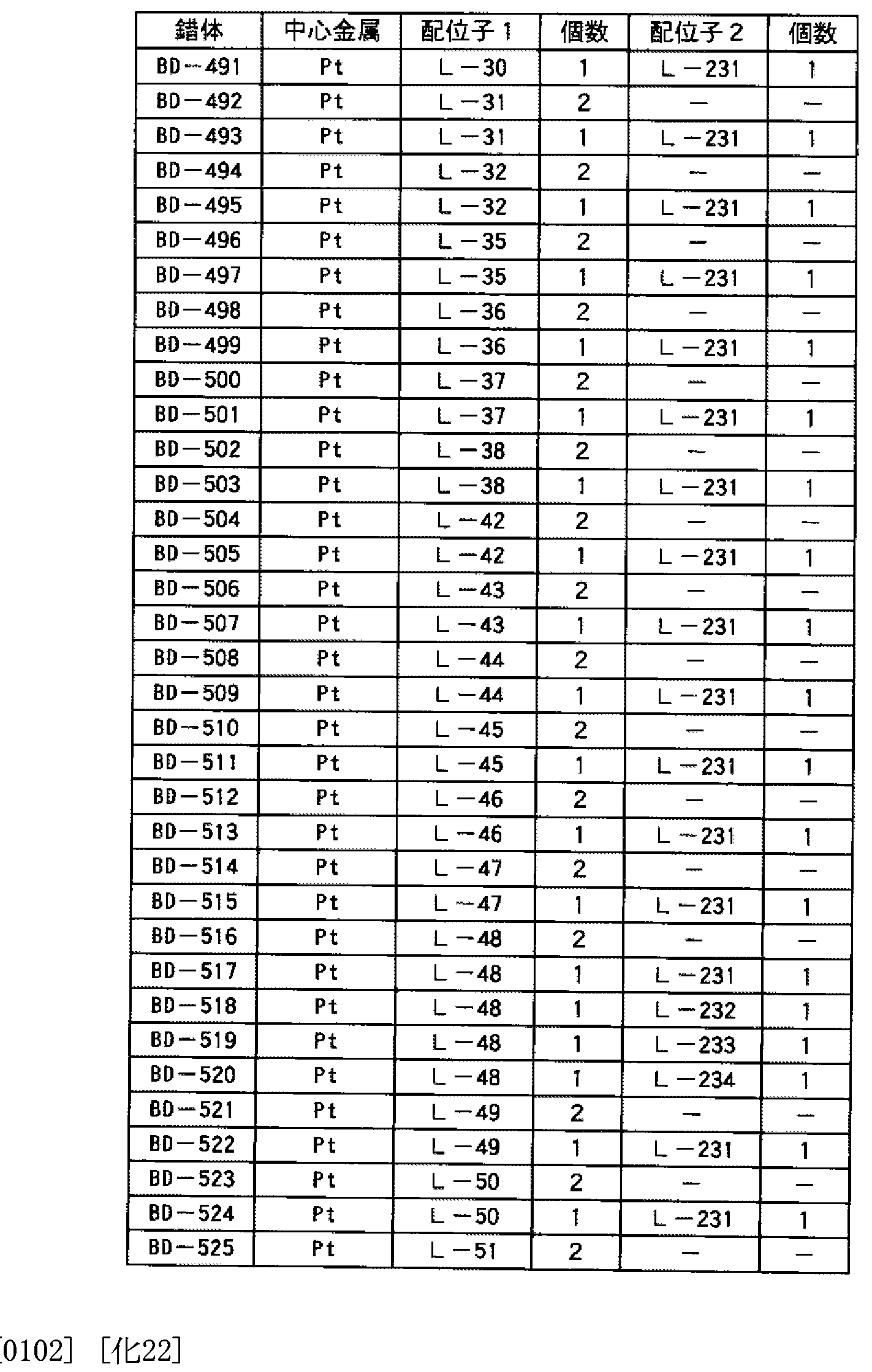


§〕〔〕50105


〕〔

へ〕〔〔0801

〕〔9010

奮〕〕〔〔

環: Z 1 環: Z 2
調節基 調節基 配位子 溶解性基の 溶解性基の
基本骨格 基本骨格 置換基 骨格 置換 1 置 骨格
R R
し一 141 Z114 R8 S - 2 R— 1 Z201 4 S— 1 R - 1 し—142 Z114 R8 S - 2 R- 1 Z201 4 S -18 R-11
L 143 Z114 R8 S -18 R— 11 Z201 4 S— 1 R- 1 し一 144 Z115; R8 = Me Z201 4 S— 1 R-■ 1
― Z201 4 S -18 R— 11 寸
し 146 Z115; R8 = Me ― Z201 4 S— 1 R— 1
L -147 Z115 R8 S— 2 R- 1 Z201 4 S— 1 R— 1
Z115 8 S— 2 R - 1 Z201 4 S -18 R-11
L一 149 Z115 R8 S 18 R— 11 Z201 4 S— 1 R— 1
L—150 Z116; R8 = II Me ― ― 一 Z201 4 S一 1 R— 1
L -151 Z116; R8 = Me Z201 4 S -18 R— 11
L -152 Z116; 8 = Me ― ― Z201 4 S - 1 R— 1
L -153 Z117 - 一 Z201 4 S— 1 R— 1
L -154 Z117 - 1201 4 S -18 R-11
L -155 Z117 Z201 4 S 1 R— 1
L -156 Z118 - ― ― Z201 4 S— 1 R— 1 し一 157 Z118 ― 一 Z201 4 S -18 R -11
L -158 Z118 - - Z201 4 S— 1 R— 1
L -159 Z119 Z201 4 S— 1 R— 1
L 160 Z119 ― Z201 4 S -18 R -11
§〕^〔2011


〕〔〕〔535011

Z1
Z101 * Z102 2 03 Z104
氺 r8、入' R M人 N"'"M 、人 R8、N人 N
4 N=N

,,

N


Z201 Z204 Z202 Z203
R=

R-13
 R一 I4 Me3
Me3Si 、木 ]

[0121] 上記一般式(1)において、 Z1で表される 5員の芳香族複素環の一例として、 Z101 〜Z145が挙げられる力 ここで、『Ν· · ·Μ』は、 5員の芳香族複素環を構成している 窒素原子と M (Irまたは Pt)との間で配位結合が形成されることを示す。
[0122] 上記一般式(1)〜(8)のいずれかにおいて、 Z2により形成される、シクロペンタジ ェン環、 6員の芳香族炭化水素環または、 5員〜 6員の芳香族複素環の一例として、 Z201〜Z218が挙げられる力 ここで、『一 M』は、 Z2により形成される環構造と M (I rまたは Pt)との結合が形成されることを示す。
[0123] また、 Z101〜Z145の各々の構造における *、 Z201〜Z218の各々の構造にお ける *、 Z1で表される環と Z2で表される環とが *を介して結合する部位を示している
[0124] 《有機 EL素子の構成層》
本発明の有機 EL素子の構成層について説明する。本発明において、有機 EL素 子の層構成の好ましい具体例を以下に示すが、本発明はこれらに限定されない。
(i)陽極 Z発光層 Z電子輸送層 Z陰極
(ii)陽極 Z正孔輸送層 Z発光層 Z電子輸送層 Z陰極
(iii)陽極 Z正孔輸送層 Z発光層 Z正孔阻止層 Z電子輸送層 Z陰極
(iv)陽極 Z正孔輸送層 Z発光層 Z正孔阻止層 Z電子輸送層 Z陰極バッファ一層
Z陰極
(v)陽極 Z陽極バッファ一層 Z正孔輸送層 Z発光層 Z正孔阻止層 Z電子輸送層 Z 陰極バッファ一層 Z陰極
本発明の有機 EL素子においては、青色発光層の発光極大波長は 430ηπ!〜 480 nmにあるものが好ましぐ緑色発光層は発光極大波長が 510nm〜550nm、赤色発 光層は発光極大波長が 600ηπ!〜 640nmの範囲にある単色発光層であることが好 ましぐこれらを用いた表示装置であることが好ましい。また、これらの少なくとも 3層の 発光層を積層して白色発光層としたものであってもよい。更に、発光層間には非発光 性の中間層を有して 、てもよ 、。本発明の有機 EL素子としては白色発光層であるこ とが好ましぐこれらを用いた照明装置であることが好ましい。
[0125] 本発明の有機 EL素子を構成する各層につ ヽて説明する。
[0126] 《発光層》
本発明に係る発光層は、電極または電子輸送層、正孔輸送層カゝら注入されてくる 電子及び正孔が再結合して発光する層であり、発光する部分は発光層の層内であつ ても発光層と隣接層との界面であってもよ 、。
[0127] 発光層の膜厚の総和は特に制限はないが、膜の均質性や、発光時に不必要な高 電圧を印加するのを防止し、かつ、駆動電流に対する発光色の安定性向上の観点 から、 2ηπι〜5 /ζ πιの範囲に調整することが好ましぐさらに好ましくは 2nm〜200n mの範囲に調整され、特に好ましくは、 ΙΟηπ!〜 20nmの範囲である。
[0128] 発光層の作製には、後述する発光ドーパントやホストイ匕合物を、例えば、真空蒸着 法、スピンコート法、キャスト法、 LB法、インクジェット法等の公知の薄膜ィ匕法により製 膜して形成することができる。
[0129] 本発明の有機 EL素子の発光層には、発光ホスト化合物と、発光ドーパント (リン光 ドーパント (リン光発光性ドーパントともいう)や蛍光ドーパント等)の少なくとも 1種類と を含有することが好ましい。
[0130] (ホスト化合物 (発光ホスト等とも 、う) )
本発明に用いられるホストイ匕合物にっ 、て説明する。
[0131] ここで、本発明においてホストイ匕合物とは、発光層に含有される化合物の内でその 層中での質量比が 20%以上であり、且つ室温(25°C)においてリン光発光のリン光 量子収率が、 0. 1未満の化合物と定義される。好ましくはリン光量子収率が 0. 01未 満である。また、発光層に含有される化合物の中で、その層中での質量比が 20%以 上であることが好ましい。
[0132] ホストイ匕合物としては、公知のホストイ匕合物を単独で用いてもよぐまたは複数種併 用して用いてもよい。ホストイ匕合物を複数種用いることで、電荷の移動を調整すること が可能であり、有機 EL素子を高効率ィ匕することができる。また、後述する発光ドーパ ントを複数種用いることで、異なる発光を混ぜることが可能となり、これにより任意の発 光色を得ることができる。
[0133] また、本発明に用いられる発光ホストとしては、従来公知の低分子化合物でも、繰り
返し単位をもつ高分子化合物でもよぐビュル基やエポキシ基のような重合性基を有 する低分子化合物 (蒸着重合性発光ホスト)でも良 ヽ。
[0134] 併用してもよい公知のホストイ匕合物としては、正孔輸送能、電子輸送能を有しつつ 、且つ発光の長波長化を防ぎ、なお且つ高 Tg (ガラス転移温度)である化合物が好 ましい。
[0135] 公知のホストイ匕合物の具体例としては、以下の文献に記載されている化合物が挙 げられる。
[0136] 特開 2001— 257076号公報、同 2002— 308855号公報、同 2001— 313179号 公報、同 2002— 319491号公報、同 2001— 357977号公報、同 2002— 334786 号公報、同 2002— 8860号公報、同 2002— 334787号公報、同 2002— 15871号 公報、同 2002— 334788号公報、同 2002— 43056号公報、同 2002— 334789 号公報、同 2002— 75645号公報、同 2002— 338579号公報、同 2002— 10544 5号公報、同 2002— 343568号公報、同 2002— 141173号公報、同 2002— 352 957号公報、同 2002— 203683号公報、同 2002— 363227号公報、同 2002— 2 31453号公報、同 2003— 3165号公報、同 2002— 234888号公報、同 2003— 2 7048号公報、同 2002— 255934号公報、同 2002— 260861号公報、同 2002— 280183号公報、同 2002— 299060号公報、同 2002— 302516号公報、同 2002 — 305083号公報、同 2002— 305084号公報、同 2002— 308837号公報等。
[0137] (発光ドーパント)
本発明に係る発光ドーパントにっ 、て説明する。
[0138] 本発明に係る発光ドーパントとしては、蛍光ドーパント (蛍光性ィ匕合物とも 、う)、リン 光ドーパント (リン光発光体、リン光性化合物、リン光発光性化合物等ともいう)を用い ることができるが、より発光効率の高い有機 EL素子を得る観点力 は、本発明の有 機 EL素子の発光層や発光ユニットに使用される発光ドーパント (単に、発光材料とい うこともある)としては、上記のホスト化合物を含有すると同時に、リン光ドーパントを含 有することが好ましい。
[0139] (リン光ドーパント)
本発明に係るリン光ドーパントにっ 、て説明する。
[0140] 本発明に係るリン光ドーパントは、励起三重項力 の発光が観測される化合物であ り、具体的には、室温 (25°C)にてリン光発光する化合物であり、リン光量子収率が、 25°Cにおいて 0. 01以上の化合物であると定義される力 好ましいリン光量子収率 は 0. 1以上である。
[0141] 上記リン光量子収率は、第 4版実験化学講座 7の分光 IIの 398頁(1992年版、丸 善)に記載の方法により測定できる。溶液中でのリン光量子収率は種々の溶媒を用 いて測定できる力 本発明に係るリン光ドーパントは、任意の溶媒のいずれかにおい て上記リン光量子収率 (0. 01以上)が達成されればょ 、。
[0142] リン光ドーパントの発光は原理としては 2種挙げられ、一つはキャリアが輸送される ホストイ匕合物上でキャリアの再結合が起こってホストイ匕合物の励起状態が生成し、こ のエネルギーをリン光ドーパントに移動させることでリン光ドーパントからの発光を得る というエネルギー移動型、もう一つはリン光ドーパントがキャリアトラップとなり、リン光ド 一パント上でキャリアの再結合が起こりリン光ドーパントからの発光が得られるというキ ャリアトラップ型であるが、いずれの場合においても、リン光ドーパントの励起状態の エネルギーはホストイ匕合物の励起状態のエネルギーよりも低いことが条件である。
[0143] リン光ドーパントは、有機 EL素子の発光層に使用される公知のものの中力 適宜 選択して用いることができる。
[0144] 本発明に係るリン光ドーパントとしては、好ましくは元素周期表で 8族〜 10族の金 属を含有する錯体系化合物であり、さらに好ましくはイリジウム化合物、オスミウム化 合物、または白金化合物(白金錯体系化合物)、希土類錯体であり、中でも最も好ま し!ヽのはイリジウム化合物である。
[0145] 以下に、リン光ドーパントとして用いられる化合物の具体例を示すが、本発明はこれ らに限定されない。これらの化合物は、例えば、 Inorg. Chem. 40卷、 1704〜171 1に記載の方法等により合成できる。
[0146] [化 40]
lr-2


[0148] [化 42]
[Zf^ [6雨]

rZ£8S0/L00Zdr/13d 19 ΐΐΙ£Ζΐ/ .ΟΟΖ OAV

[0151] [化 45]
h-1 h Rh-3

[0152] (蛍光ドーパント (蛍光性ィ匕合物とも!、う) )
蛍光ドーパント (蛍光性ィ匕合物)としては、クマリン系色素、ピラン系色素、シァニン 系色素、クロコニゥム系色素、スクァリウム系色素、ォキソベンツアントラセン系色素、 フルォレセイン系色素、ローダミン系色素、ピリリウム系色素、ペリレン系色素、スチル ベン系色素、ポリチオフ ン系色素、または希土類錯体系蛍光体等が挙げられる。
[0153] 次に、本発明の有機 EL素子の構成層として用いられる、注入層、阻止層、電子輸 送層等について説明する。
[0154] 《注入層:電子注入層、正孔注入層》
注入層は必要に応じて設け、電子注入層と正孔注入層があり、上記の如く陽極と 発光層または正孔輸送層の間、及び陰極と発光層または電子輸送層との間に存在 させてちょい。
[0155] 注入層とは、駆動電圧低下や発光輝度向上のために電極と有機層間に設けられる 層のことで、「有機 EL素子とその工業化最前線( 1998年 11月 30日ェヌ'ティー ·ェ ス社発行)」の第 2編第 2章「電極材料」(123〜166頁)に詳細に記載されており、正 孔注入層(陽極バッファ一層)と電子注入層(陰極バッファ一層)とがある。
[0156] 陽極バッファ一層(正孔注入層)は、特開平 9— 45479号公報、同 9 260062号 公報、同 8— 288069号公報等にもその詳細が記載されており、具体例として、銅フ タロシアニンに代表されるフタロシアニンバッファ一層、酸ィ匕バナジウムに代表される 酸化物バッファ一層、アモルファスカーボンバッファ一層、ポリア-リン(ェメラルディ ン)やポリチォフェン等の導電性高分子を用いた高分子バッファ一層等が挙げられる
[0157] 陰極バッファ一層(電子注入層)は、特開平 6— 325871号公報、同 9 17574号 公報、同 10— 74586号公報等にもその詳細が記載されており、具体的にはストロン チウムゃアルミニウム等に代表される金属バッファ一層、フッ化リチウムに代表される アルカリ金属化合物バッファ一層、フッ化マグネシウムに代表されるアルカリ土類金 属化合物バッファ一層、酸ィヒアルミニウムに代表される酸ィヒ物バッファ一層等が挙げ られる。上記バッファ一層(注入層)はごく薄い膜であることが望ましぐ素材にもよる がその膜厚は 0. lnm〜5 mの範囲が好ましい。
[0158] 《阻止層:正孔阻止層、電子阻止層》
阻止層は、上記の如く有機化合物薄膜の基本構成層の他に必要に応じて設けら れるものである。例えば、特開平 11 204258号公報、同 11— 204359号公報、及 び「有機 EL素子とその工業化最前線( 1998年 11月 30日ェヌ'ティー ·エス社発行) 」の 237頁等に記載されて 、る正孔阻止(ホールブロック)層がある。
[0159] 正孔阻止層とは広い意味では電子輸送層の機能を有し、電子を輸送する機能を有 しつつ正孔を輸送する能力が著しく小さい正孔阻止材料力 なり、電子を輸送しつ つ正孔を阻止することで電子と正孔の再結合確率を向上させることができる。また、 後述する電子輸送層の構成を必要に応じて、本発明に係わる正孔阻止層として用い ることがでさる。
[0160] 本発明の有機 EL素子の正孔阻止層は、発光層に隣接して設けられていることが好 ましい。
[0161] 正孔阻止層には、前述のホストイ匕合物として挙げたァザカルバゾール誘導体を含 有することが好ましい。
[0162] また、本発明においては、複数の発光色の異なる複数の発光層を有する場合、そ の発光極大波長が最も短波にある発光層が、全発光層中、最も陽極に近いことが好 ましいが、このような場合、該最短波層と該層の次に陽極に近い発光層との間に正孔 阻止層を追加して設けることが好ましい。更には、該位置に設けられる正孔阻止層に 含有される化合物の 50質量%以上が、前記最短波発光層のホスト化合物に対しそ のイオン化ポテンシャルが 0. 3eV以上大き!/、ことが好まし!/、。
[0163] イオンィ匕ポテンシャルは化合物の HOMO (最高被占分子軌道)レベルにある電子
を真空準位に放出するのに必要なエネルギーで定義され、例えば下記に示すような 方法により求めることができる。
[0164] (1)米国 Gaussian社製の分子軌道計算用ソフトウェアである Gaussian98 (Gauss ian98、 Revision A. 丄 1. 4, M. J. Frisch, et al, Lraussian, Inc. , Pittsburg h PA, 2002. )を用い、キーワードとして B3LYPZ6— 31G *を用いて構造最適 化を行うことにより算出した値 (eV単位換算値)の小数点第 2位を四捨五入した値とし てイオン化ポテンシャルを求めることができる。この計算値が有効な背景には、この手 法で求めた計算値と実験値の相関が高いためである。
[0165] (2)イオンィ匕ポテンシャルは光電子分光法で直接測定する方法により求めることも できる。例えば、理研計器社製の低エネルギー電子分光装置「Model AC— 1」を 用いて、あるいは紫外光電子分光として知られて 、る方法を好適に用いることができ る。
[0166] 一方、電子阻止層とは広い意味では正孔輸送層の機能を有し、正孔を輸送する機 能を有しつつ電子を輸送する能力が著しく小さい材料力 なり、正孔を輸送しつつ電 子を阻止することで電子と正孔の再結合確率を向上させることができる。また、後述 する正孔輸送層の構成を必要に応じて電子阻止層として用いることができる。本発明 に係る正孔阻止層、電子輸送層の膜厚としては、好ましくは 3ηπ!〜 lOOnmであり、 更に好ましくは 5ηπ!〜 30nmである。
[0167] 《正孔輸送層》
正孔輸送層とは正孔を輸送する機能を有する正孔輸送材料力 なり、広い意味で 正孔注入層、電子阻止層も正孔輸送層に含まれる。正孔輸送層は単層または複数 層設けることができる。
[0168] 正孔輸送材料としては、正孔の注入または輸送、電子の障壁性の 、ずれかを有す るものであり、有機物、無機物のいずれであってもよい。例えば、トリァゾール誘導体 、ォキサジァゾール誘導体、イミダゾール誘導体、ポリアリールアルカン誘導体、ビラ ゾリン誘導体及びピラゾロン誘導体、フ -レンジァミン誘導体、ァリールァミン誘導 体、ァミノ置換カルコン誘導体、ォキサゾール誘導体、スチリルアントラセン誘導体、 フルォレノン誘導体、ヒドラゾン誘導体、スチルベン誘導体、シラザン誘導体、ァニリ
ン系共重合体、また導電性高分子オリゴマー、特にチォフェンオリゴマー等が挙げら れる。
[0169] 正孔輸送材料としては上記のものを使用することができる力 ボルフイリンィ匕合物、 芳香族第 3級ァミン化合物及びスチリルアミン化合物、特に芳香族第 3級アミンィ匕合 物を用いることが好ましい。
[0170] 芳香族第 3級アミンィ匕合物及びスチリルアミンィ匕合物の代表例としては、 N, N, N ' , N' —テトラフエニル一 4, 4' —ジァミノフエ-ル; N, N' —ジフエ-ル一 N, N ' —ビス(3—メチルフエ-ル)一〔1, 1' —ビフエ-ル〕一 4, 4' —ジァミン(TPD) ; 2, 2 ビス(4 ジ一 p トリルァミノフエ-ル)プロパン; 1, 1—ビス(4 ジ一 p トリ ルァミノフエ-ル)シクロへキサン; N, N, N' , N' —テトラ一 p トリル一 4, 4' - ジアミノビフエ-ル; 1 , 1 ビス(4 ジ一 p トリルァミノフエ-ル) 4 フエ-ルシク 口へキサン;ビス(4 -ジメチルァミノ 2 メチルフエ-ル)フエニルメタン;ビス(4 -ジ —p トリルァミノフエ-ル)フエ-ルメタン; N, N' —ジフエ-ル一 N, N' —ジ(4— メトキシフエ-ル) 4, 4' ージアミノビフエニル; N, N, N' , N' —テトラフエ-ル —4, 4' ージアミノジフエ-ルエーテル; 4, 4' ビス(ジフエ-ルァミノ)クオ一ドリフ ェ -ル; N, N, N トリ(p トリル)ァミン; 4— (ジ— p トリルァミノ)— 4' —〔4— (ジ —p トリルァミノ)スチリル〕スチルベン; 4— N, N ジフエ-ルァミノ—(2 ジフエ- ルビ-ル)ベンゼン; 3—メトキシ一 4' — N, N ジフエニルアミノスチルベンゼン; N フエ-ルカルバゾール、更には米国特許第 5, 061 , 569号明細書に記載されて いる 2個の縮合芳香族環を分子内に有するもの、例えば、 4, 4' ビス〔N—(1ーナ フチル) N フエ-ルァミノ〕ビフヱ-ル(NPD)、特開平 4 308688号公報に記 載されているトリフエ-ルァミンユニットが 3つスターバースト型に連結された 4, 4' , A" —トリス〔?^— (3—メチルフエ-ル) N フエ-ルァミノ〕トリフエ-ルァミン(MTD ATA)等が挙げられる。
[0171] 更にこれらの材料を高分子鎖に導入した、またはこれらの材料を高分子の主鎖とし た高分子材料を用いることもできる。また、 P型— Si、 p型— SiC等の無機化合物も正 孔注入材料、正孔輸送材料として使用することができる。
[0172] また、特開平 11— 251067号公報、 J. Huang et. al.著文献 (Applied Physic
s Letters 80 (2002) , p. 139)に記載されているような、所謂 p型正孔輸送材料 を用いることもできる。本発明においては、より高効率の発光素子が得られることから これらの材料を用いることが好まし!/、。
[0173] 正孔輸送層は上記正孔輸送材料を、例えば、真空蒸着法、スピンコート法、キャス ト法、インクジェット法を含む印刷法、 LB法等の公知の方法により、薄膜ィ匕することに より形成することができる。正孔輸送層の膜厚については特に制限はないが、通常は 5nm〜5 μ m程度、好ましくは 5nm〜200nmである。この正孔輸送層は上記材料の 1種または 2種以上力もなる一層構造であってもよ 、。
[0174] また、不純物をドープした p性の高い正孔輸送層を用いることもできる。その例とし ては、特開平 4— 297076号公報、特開 2000— 196140号公報、同 2001— 1021 75号公報の各公報、 J. Appl. Phys. , 95, 5773 (2004)等に記載されたものが挙 げられる。
[0175] 本発明においては、このような ρ性の高い正孔輸送層を用いることが、より低消費電 力の素子を作製することができるため好ましい。
[0176] 《電子輸送層》
電子輸送層とは電子を輸送する機能を有する材料力 なり、広い意味で電子注入 層、正孔阻止層も電子輸送層に含まれる。電子輸送層は単層または複数層設けるこ とがでさる。
[0177] 従来、単層の電子輸送層、及び複数層とする場合は発光層に対して陰極側に隣 接する電子輸送層に用いられる電子輸送材料 (正孔阻止材料を兼ねる)としては、陰 極より注入された電子を発光層に伝達する機能を有していればよぐその材料として は従来公知の化合物の中から任意のものを選択して用いることができ、例えば、 -ト 口置換フルオレン誘導体、ジフヱ-ルキノン誘導体、チォピランジオキシド誘導体、力 ルボジイミド、フレオレニリデンメタン誘導体、アントラキノジメタン及びアントロン誘導 体、ォキサジァゾール誘導体等が挙げられる。更に上記ォキサジァゾール誘導体に ぉ 、て、ォキサジァゾール環の酸素原子を硫黄原子に置換したチアジアゾール誘導 体、電子吸引基として知られているキノキサリン環を有するキノキサリン誘導体も、電 子輸送材料として用いることができる。更にこれらの材料を高分子鎖に導入した、ま
たはこれらの材料を高分子の主鎖とした高分子材料を用いることもできる。
[0178] また 8 キノリノール誘導体の金属錯体、例えば、トリス(8 キノリノール)アルミ-ゥ ム(Alq)、トリス(5, 7—ジクロロ一 8—キノリノール)アルミニウム、トリス(5, 7—ジブ口 モ一 8 キノリノール)アルミニウム、トリス(2 メチル 8 キノリノール)アルミニウム 、トリス(5—メチル 8—キノリノール)アルミニウム、ビス(8—キノリノール)亜鉛(Znq )等、及びこれらの金属錯体の中心金属が In、 Mg、 Cu、 Ca、 Sn、 Gaまたは Pbに置 き替わった金属錯体も、電子輸送材料として用いることができる。その他、メタルフリ 一もしくはメタルフタロシアニン、またはそれらの末端がアルキル基ゃスルホン酸基等 で置換されているものも、電子輸送材料として好ましく用いることができる。また、発光 層の材料として例示したジスチリルビラジン誘導体も、電子輸送材料として用いること 力 Sできるし、正孔注入層、正孔輸送層と同様に n型 Si、 n型 SiC等の無機半導体 も電子輸送材料として用いることができる。
[0179] 電子輸送層は上記電子輸送材料を、例えば、真空蒸着法、スピンコート法、キャス ト法、インクジェット法を含む印刷法、 LB法等の公知の方法により、薄膜ィ匕することに より形成することができる。電子輸送層の膜厚については特に制限はないが、通常は 5nm〜5 μ m程度、好ましくは 5ηπ!〜 200nmである。電子輸送層は上記材料の 1種 または 2種以上力もなる一層構造であってもよ 、。
[0180] また、不純物をドープした n性の高い電子輸送層を用いることもできる。その例とし ては、特開平 4— 297076号公報、同 10— 270172号公報、特開 2000— 196140 号公報、同 2001— 102175号公報、 Appl. Phys. , 95, 5773 (2004)等に記載 されたものが挙げられる。
[0181] 本発明においては、このような η性の高い電子輸送層を用いることがより低消費電 力の素子を作製することができるため好ましい。
[0182] 《陽極》
有機 EL素子における陽極としては、仕事関数の大きい (4eV以上)金属、合金、電 気伝導性化合物及びこれらの混合物を電極物質とするものが好ましく用いられる。こ のような電極物質の具体例としては、 Au等の金属、 Cul、インジウムチンォキシド (IT 0)、 SnO、 ZnO等の導電性透明材料が挙げられる。また、 IDIXO (In O—ZnO)
等非晶質で透明導電膜を作製可能な材料を用いてもよ!ヽ。陽極はこれらの電極物 質を蒸着やスパッタリング等の方法により薄膜を形成させ、フォトリソグラフィ一法で所 望の形状のパターンを形成してもよぐあるいはパターン精度をあまり必要としない場 合は(100 μ m以上程度)、上記電極物質の蒸着やスパッタリング時に所望の形状の マスクを介してパターンを形成してもよい。あるいは、有機導電性ィ匕合物のように塗布 可能な物質を用いる場合には、印刷方式、コーティング方式等湿式製膜法を用いる こともできる。この陽極より発光を取り出す場合には、透過率を 10%より大きくすること が望ましぐまた陽極としてのシート抵抗は数百 Ω Ζ口以下が好ましい。更に膜厚は 材料にもよるが、通常は、 10nm〜1000nmの範囲であり、好ましくは 10nm〜200n mの範囲で選ばれる。
[0183] 《陰極》
一方、陰極としては仕事関数の小さ ヽ (4eV以下)金属 (電子注入性金属と称する) 、合金、電気伝導性化合物及びこれらの混合物を電極物質とするものが用いられる。 このような電極物質の具体例としては、ナトリウム、ナトリウム一カリウム合金、マグネシ ゥム、リチウム、マグネシウム Z銅混合物、マグネシウム Z銀混合物、マグネシウム Z アルミニウム混合物、マグネシウム Zインジウム混合物、アルミニウム Z酸ィ匕アルミ- ゥム (Al O )
2 3混合物、インジウム、リチウム Zアルミニウム混合物、希土類金属等が挙 げられる。これらの中で、電子注入性及び酸ィ匕等に対する耐久性の点から、電子注 入性金属とこれより仕事関数の値が大きく安定な金属である第二金属との混合物、 例えば、マグネシウム Z銀混合物、マグネシウム Zアルミニウム混合物、マグネシウム Zインジウム混合物、アルミニウム Z酸ィ匕アルミニウム (Al O )混合物、リチウム
2 3 Zァ ルミ-ゥム混合物、アルミニウム等が好適である。陰極はこれらの電極物質を蒸着や スパッタリング等の方法により薄膜を形成させることにより、作製することができる。ま た、陰極としてのシート抵抗は数百 Ω Ζ口以下が好ましぐ膜厚は通常 ΙΟηπ!〜 5 m、好ましくは 50nm〜200nmの範囲で選ばれる。尚、発光した光を透過させるため 、有機 EL素子の陽極または陰極のいずれか一方が透明または半透明であれば発 光輝度が向上し好都合である。
[0184] また、陰極に上記金属を Inn!〜 20nmの膜厚で作製した後に、陽極の説明で挙げ
た導電性透明材料をその上に作製することで、透明または半透明の陰極を作製する ことができ、これを応用することで陽極と陰極の両方が透過性を有する素子を作製す ることがでさる。
[0185] 《支持基板》
本発明の有機 EL素子に用いることのできる支持基板 (以下、基体、基板、基材、支 持体等とも言う)としては、ガラス、プラスチック等の種類には特に限定はなぐまた透 明であっても不透明であってもよい。支持基板側力 光を取り出す場合には、支持基 板は透明であることが好ましい。好ましく用いられる透明な支持基板としては、ガラス 、石英、透明榭脂フィルムを挙げることができる。特に好ましい支持基板は、有機 EL 素子にフレキシブル性を与えることが可能な榭脂フィルムである。
[0186] 榭脂フィルムとしては、例えば、ポリエチレンテレフタレート(PET)、ポリエチレンナ フタレート(PEN)等のポリエステル、ポリエチレン、ポリプロピレン、セロファン、セル口 ースジアセテート、セノレローストリアセテート、セノレロースアセテートブチレート、セノレ口 ースアセテートプロピオネート(CAP)、セルロースアセテートフタレート(TAC)、セル ロースナイトレート等のセルロースエステル類またはそれらの誘導体、ポリ塩ィ匕ビユリ デン、ポリビュルアルコール、ポリエチレンビュルアルコール、シンジォタクティックポ リスチレン、ポリカーボネート、ノルボルネン榭脂、ポリメチルペンテン、ポリエーテルケ トン、ポリイミド、ポリエーテルスルホン(PES)、ポリフエ-レンスルフイド、ポリスルホン 類、ポリエーテルイミド、ポリエーテルケトンイミド、ポリアミド、フッ素榭脂、ナイロン、ポ リメチルメタタリレート、アクリルあるいはポリアリレート類、アートン (商品名 JSR社製) あるいはアベル (商品名三井化学社製) 、つたシクロォレフイン系榭脂等を挙げら れる。
[0187] 榭脂フィルムの表面には、無機物、有機物の被膜またはその両者のノ、イブリツド被 膜が形成されていてもよぐ JIS K 7129— 1992に準拠した方法で測定された、水 蒸気透過度(25 ±0. 5°C、相対湿度(90± 2) %RH)が 0. 01g/ (m2' 24h)以下の ノ リア性フィルムであることが好ましぐ更には、 JIS K 7126— 1987に準拠した方 法で測定された酸素透過度が、 10—3ml/ (m2· 24hr·MPa)以下、水蒸気透過度が 、 10— 5g/ (m2' 24h)以下の高バリア性フィルムであることが好ましい。
[0188] バリア膜を形成する材料としては、水分や酸素等素子の劣化をもたらすものの浸入 を抑制する機能を有する材料であればよぐ例えば、酸化珪素、二酸化珪素、窒化 珪素等を用いることができる。更に該膜の脆弱性を改良するために、これら無機層と 有機材料からなる層の積層構造を持たせることがより好ましい。無機層と有機層の積 層順については特に制限はないが、両者を交互に複数回積層させることが好ましい
[0189] バリア膜の形成方法については特に限定はなぐ例えば、真空蒸着法、スパッタリ ング法、反応性スパッタリング法、分子線エピタキシー法、クラスターイオンビーム法、 イオンプレーティング法、プラズマ重合法、大気圧プラズマ重合法、プラズマ CVD法 、レーザー CVD法、熱 CVD法、コーティング法等を用いることができる力 特開 200 4— 68143号公報に記載されているような大気圧プラズマ重合法によるものが特に 好ましい。
[0190] 不透明な支持基板としては、例えば、アルミ、ステンレス等の金属板、フィルムゃ不 透明榭脂基板、セラミック製の基板等が挙げられる。
[0191] 本発明の有機 EL素子の発光の室温における外部取り出し効率は、 1%以上である ことが好ましぐより好ましくは 5%以上である。ここに、外部取り出し量子効率(%) = 有機 EL素子外部に発光した光子数 Z有機 EL素子に流した電子数 X 100である。
[0192] また、カラーフィルタ一等の色相改良フィルタ一等を併用しても、有機 EL素子から の発光色を蛍光体を用いて多色へ変換する色変換フィルターを併用してもよ ヽ。色 変換フィルターを用いる場合においては、有機 EL素子の発光の λ maxは 480nm以 下が好ましい。
[0193] 《封止》
本発明に用いられる封止手段としては、例えば、封止部材と電極、支持基板とを接 着剤で接着する方法を挙げることができる。
[0194] 封止部材としては、有機 EL素子の表示領域を覆うように配置されておればよぐ凹 板状でも平板状でもよい。また透明性、電気絶縁性は特に問わない。
[0195] 具体的には、ガラス板、ポリマー板'フィルム、金属板'フィルム等が挙げられる。ガ ラス板としては、特にソーダ石灰ガラス、ノ リウム 'ストロンチウム含有ガラス、鉛ガラス
、アルミノケィ酸ガラス、ホウケィ酸ガラス、ノ リウムホウケィ酸ガラス、石英等を挙げる ことができる。また、ポリマー板としては、ポリカーボネート、アクリル、ポリエチレンテレ フタレート、ポリエーテルサルファイド、ポリサルフォン等を挙げることができる。金属板 としては、ステンレス、鉄、銅、アルミニウム、マグネシウム、ニッケル、亜鉛、クロム、チ タン、モリブテン、シリコン、ゲルマニウム及びタンタル力 なる群力 選ばれる一種以 上の金属または合金力もなるものが挙げられる。
[0196] 本発明においては、素子を薄膜ィ匕できるということからポリマーフィルム、金属フィル ムを好ましく使用することができる。更には、ポリマーフィルムは、 JIS K 7126- 19 87に準拠した方法で測定された酸素透過度が 1 X 10"3ml/ (m2- 24hr-MPa)以下 、JIS K 7129— 1992に準拠した方法で測定された、水蒸気透過度(25±0. 5°C 、相対湿度(90± 2) %RH)が、 1 X 10— 3g/ (m2' 24h)以下のものであることが好ま しい。
[0197] 封止部材を凹状に加工するのは、サンドブラスト加工、化学エッチング加工等が使 われる。
[0198] 接着剤として具体的には、アクリル酸系オリゴマー、メタクリル酸系オリゴマーの反応 性ビュル基を有する光硬化及び熱硬化型接着剤、 2 シァノアクリル酸エステル等 の湿気硬化型等の接着剤を挙げることができる。また、エポキシ系等の熱及び化学 硬化型(二液混合)を挙げることができる。また、ホットメルト型のポリアミド、ポリエステ ル、ポリオレフインを挙げることができる。また、カチオン硬化タイプの紫外線硬化型 エポキシ榭脂接着剤を挙げることができる。
[0199] なお、有機 EL素子が熱処理により劣化する場合があるので、室温力 80°Cまでに 接着硬化できるものが好ましい。また、前記接着剤中に乾燥剤を分散させておいても よい。封止部分への接着剤の塗布は市販のディスペンサーを使ってもよいし、スクリ ーン印刷のように印刷してもよ!/、。
[0200] また、有機層を挟み支持基板と対向する側の電極の外側に該電極と有機層を被覆 し、支持基板と接する形で無機物、有機物の層を形成し封止膜とすることも好適にで きる。この場合、該膜を形成する材料としては、水分や酸素等素子の劣化をもたらす ものの浸入を抑制する機能を有する材料であればよぐ例えば、酸化珪素、二酸ィ匕
珪素、窒化珪素等を用いることができる。更に該膜の脆弱性を改良するために、これ ら無機層と有機材料カゝらなる層の積層構造を持たせることが好ましい。これらの膜の 形成方法については、特に限定はなぐ例えば真空蒸着法、スパッタリング法、反応 性スパッタリング法、分子線エピタキシー法、クラスターイオンビーム法、イオンプレー ティング法、プラズマ重合法、大気圧プラズマ重合法、プラズマ CVD法、レーザー C VD法、熱 CVD法、コーティング法等を用いることができる。
[0201] 封止部材と有機 EL素子の表示領域との間隙には、気相及び液相では、窒素、ァ ルゴン等の不活性気体やフッ化炭化水素、シリコンオイルのような不活性液体を注入 することが好ましい。また真空とすることも可能である。また、内部に吸湿性ィ匕合物を 封人することちでさる。
[0202] 吸湿性ィ匕合物としては、例えば、金属酸化物(例えば、酸ィ匕ナトリウム、酸ィ匕カリウム 、酸ィ匕カルシウム、酸化バリウム、酸化マグネシウム、酸ィ匕アルミニウム等)、硫酸塩( 例えば、硫酸ナトリウム、硫酸カルシウム、硫酸マグネシウム、硫酸コバルト等)、金属 ハロゲン化物(例えば、塩化カルシウム、塩化マグネシウム、フッ化セシウム、フッ化タ ンタル、臭化セリウム、臭化マグネシウム、沃化ノ リウム、沃化マグネシウム等)、過塩 素酸類 (例えば、過塩素酸バリウム、過塩素酸マグネシウム等)等が挙げられ、硫酸 塩、金属ハロゲン化物及び過塩素酸類にぉ 、ては無水塩が好適に用いられる。
[0203] 《保護膜、保護板》
有機層を挟み支持基板と対向する側の前記封止膜、あるいは前記封止用フィルム の外側に、素子の機械的強度を高めるために保護膜、あるいは保護板を設けてもよ い。特に封止が前記封止膜により行われている場合には、その機械的強度は必ずし も高くないため、このような保護膜、保護板を設けることが好ましい。これに使用するこ とができる材料としては、前記封止に用いたのと同様なガラス板、ポリマー板'フィル ム、金属板'フィルム等を用いることができる力 軽量且つ薄膜ィ匕ということからポリマ 一フィルムを用いることが好まし 、。
[0204] 《光取り出し》
有機 EL素子は空気よりも屈折率の高い (屈折率が 1. 7〜2. 1程度)層の内部で発 光し、発光層で発生した光のうち 15%から 20%程度の光しか取り出せないことがー
般的に言われている。これは、臨界角以上の角度 Θで界面 (透明基板と空気との界 面)に入射する光は、全反射を起こし素子外部に取り出すことができないことや、透明 電極な 、し発光層と透明基板との間で光が全反射を起こし、光が透明電極な 、し発 光層を導波し、結果として光が素子側面方向に逃げるためである。
[0205] この光の取り出しの効率を向上させる手法としては、例えば、透明基板表面に凹凸 を形成し、透明基板と空気界面での全反射を防ぐ方法 (米国特許第 4, 774, 435号 明細書)、基板に集光性を持たせることにより効率を向上させる方法 (特開昭 63— 31 4795号公報)、素子の側面等に反射面を形成する方法 (特開平 1— 220394号公 報)、基板と発光体の間に中間の屈折率を持つ平坦層を導入し、反射防止膜を形成 する方法 (特開昭 62— 172691号公報)、基板と発光体の間に基板よりも低屈折率 を持つ平坦層を導入する方法 (特開 2001— 202827号公報)、基板、透明電極層 や発光層のいずれかの層間 (含む、基板と外界間)に回折格子を形成する方法 (特 開平 11― 283751号公報)等がある。
[0206] 本発明においては、これらの方法を本発明の有機 EL素子と組み合わせて用いるこ とができるが、基板と発光体の間に基板よりも低屈折率を持つ平坦層を導入する方 法、あるいは基板、透明電極層や発光層のいずれかの層間 (含む、基板と外界間) に回折格子を形成する方法を好適に用いることができる。
[0207] 本発明はこれらの手段を組み合わせることにより、更に高輝度あるいは耐久性に優 れた素子を得ることができる。
[0208] 透明電極と透明基板の間に低屈折率の媒質を光の波長よりも長い厚みで形成する と、透明電極から出てきた光は、媒質の屈折率が低いほど外部への取り出し効率が 高くなる。
[0209] 低屈折率層としては、例えば、エア口ゲル、多孔質シリカ、フッ化マグネシウム、フッ 素系ポリマー等が挙げられる。透明基板の屈折率は一般に 1. 5〜1. 7程度であるの で、低屈折率層は屈折率がおよそ 1. 5以下であることが好ましい。また、更に 1. 35 以下であることが好ましい。
[0210] また、低屈折率媒質の厚みは媒質中の波長の 2倍以上となるのが望ましい。これは 低屈折率媒質の厚みが、光の波長程度になってエバネッセントで染み出した電磁波
が基板内に入り込む膜厚になると、低屈折率層の効果が薄れるからである。
[0211] 全反射を起こす界面もしくはいずれかの媒質中に回折格子を導入する方法は、光 取り出し効率の向上効果が高 、と 、う特徴がある。この方法は回折格子が 1次の回 折や 2次の回折といった所謂ブラッグ回折により、光の向きを屈折とは異なる特定の 向きに変えることができる性質を利用して、発光層から発生した光のうち層間での全 反射等により外に出ることができない光を、いずれかの層間もしくは、媒質中 (透明基 板内や透明電極内)に回折格子を導入することで光を回折させ、光を外に取り出そう とするちのである。
[0212] 導入する回折格子は、二次元的な周期屈折率を持っていることが望ましい。これは 発光層で発光する光はあらゆる方向にランダムに発生するので、ある方向にのみ周 期的な屈折率分布を持っている一般的な 1次元回折格子では、特定の方向に進む 光しか回折されず、光の取り出し効率がさほど上がらない。しかしながら、屈折率分 布を二次元的な分布にすることにより、あらゆる方向に進む光が回折され、光の取り 出し効率が上がる。
[0213] 回折格子を導入する位置としては前述の通り、いずれかの層間もしくは媒質中 (透 明基板内や透明電極内)でもよいが、光が発生する場所である有機発光層の近傍が 望ましい。
[0214] このとき、回折格子の周期は媒質中の光の波長の約 1Z2〜3倍程度が好ましい。
[0215] 回折格子の配列は正方形のラチス状、三角形のラチス状、ハニカムラチス状等、 2 次元的に配列が繰り返されることが好ましい。
[0216] 《集光シート》
本発明の有機 EL素子は基板の光取り出し側に、例えば、マイクロレンズアレイ状の 構造を設けるように加工したり、あるいは所謂集光シートと組み合わせることにより、特 定方向、例えば、素子発光面に対し正面方向に集光することにより、特定方向上の 輝度を高めることができる。
[0217] マイクロレンズアレイの例としては、基板の光取り出し側に一辺が 30 μ mでその頂 角が 90度となるような四角錐を 2次元に配列する。一辺は 10 /z m〜: LOO /z mが好ま しい。これより小さくなると回折の効果が発生して色付ぐ大きすぎると厚みが厚くなり
好ましくない。
[0218] 集光シートとしては、例えば、液晶表示装置の LEDバックライトで実用化されている ものを用いることが可能である。このようなシートとして、例えば、住友スリーェム社製 輝度上昇フィルム (BEF)等を用いることができる。プリズムシートの形状としては、例 えば、基材に頂角 90度、ピッチ 50 111の 状のストライプが形成されたものであって もよいし、頂角が丸みを帯びた形状、ピッチをランダムに変化させた形状、その他の 形状であってもよい。
[0219] また、発光素子からの光放射角を制御するために、光拡散板'フィルムを集光シー トと併用してもよい。例えば、(株)きもと製拡散フィルム (ライトアップ)等を用いること ができる。
[0220] 《有機 EL素子の作製方法》
本発明の有機 EL素子の作製方法の一例として、陽極/正孔注入層/正孔輸送層 Z発光層 Z電子輸送層 Z電子注入層 Z陰極からなる有機 EL素子の作製法を説明 する。
[0221] まず適当な基体上に所望の電極物質、例えば、陽極用物質力 なる薄膜を 1 μ m 以下、好ましくは ΙΟηπ!〜 200nmの膜厚になるように、蒸着やスパッタリング等の方 法により形成させ陽極を作製する。
[0222] 次に、この上に有機 EL素子材料である正孔注入層、正孔輸送層、発光層、電子輸 送層、電子注入層、正孔阻止層の有機化合物薄膜を形成させる。
[0223] これら各層の形成方法としては、前記の如く蒸着法、ウエットプロセス (スピンコート 法、キャスト法、インクジェット法、印刷法)等があるが、均質な膜が得られやすぐ且 つピンホールが生成しにくい等の点から、本発明においてはスピンコート法、インクジ エツト法、印刷法等の塗布法による製膜が好ま U、。
[0224] 本発明に係る有機 EL材料を溶解または分散する液媒体としては、例えば、メチル ェチルケトン、シクロへキサノン等のケトン類、酢酸ェチル等の脂肪酸エステル類、ジ クロ口ベンゼン等のハロゲン化炭化水素類、トルエン、キシレン、メシチレン、シクロへ キシルベンゼン等の芳香族炭化水素類、シクロへキサン、デカリン、ドデカン等の脂 肪族炭化水素類、 DMF、 DMSO等の有機溶媒を用いることができる。また分散方
法としては、超音波、高剪断力分散やメディア分散等の分散方法により分散すること ができる。
[0225] これらの層を形成後、その上に陰極用物質力もなる薄膜を 1 μ m以下、好ましくは、 50nm〜200nmの範囲の膜厚になるように、例えば、蒸着やスパッタリング等の方法 により形成させ、陰極を設けることにより所望の有機 EL素子が得られる。
[0226] また作製順序を逆にして、陰極、電子注入層、電子輸送層、発光層、正孔輸送層、 正孔注入層、陽極の順に作製することも可能である。このようにして得られた多色の 表示装置に、直流電圧を印加する場合には陽極を +、陰極を一の極性として電圧 2 〜40V程度を印加すると発光が観測できる。また交流電圧を印加してもよい。なお、 印加する交流の波形は任意でょ 、。
[0227] 《用途》
本発明の有機 EL素子は、表示デバイス、ディスプレイ、各種発光光源として用いる ことができる。発光光源として、例えば、照明装置 (家庭用照明、車内照明)、時計や 液晶用バックライト、看板広告、信号機、光記憶媒体の光源、電子写真複写機の光 源、光通信処理機の光源、光センサーの光源等が挙げられるがこれに限定するもの ではないが、特に液晶表示装置のバックライト、照明用光源としての用途に有効に用 いることがでさる。
[0228] 本発明の有機 EL素子においては、必要に応じ製膜時にメタルマスクやインクジエツ トプリンティング法等でパターユングを施してもよい。パターユングする場合は、電極 のみをパターユングしてもよいし、電極と発光層をパターユングしてもよいし、素子全 層をパターユングしてもよぐ素子の作製においては、従来公知の方法を用いること ができる。
[0229] 本発明の有機 EL素子や本発明に係る化合物の発光する色は、「新編色彩科学ハ ンドブック」(日本色彩学会編、東京大学出版会、 1985)の 108頁の図 4. 16におい て、分光放射輝度計 CS - 1000 (コ-力ミノルタセンシング社製)で測定した結果を C IE色度座標に当てはめたときの色で決定される。
[0230] また、本発明の有機 EL素子が白色素子の場合には、白色とは、 2度視野角正面輝 度を上記方法により測定した際に、 1000CdZm2での CIE1931表色系における色
度力 ¾ =0. 33±0. 07、 Y=0. 33±0. 1の領域内にあることを言う。
実施例
[0231] 以下、実施例により本発明を説明するが、本発明はこれらに限定されない。
[0232] また、以下に実施例で使用する化合物の構造を示す。
[0233] [化 46]


[0234] 実施例 1
《例示化合物 BD— 6の合成》
以下のようにして、配位子 L— 3を合成し、次いで、配位子 L— 3を用いて、本発明 の例示化合物 BD— 6を合成した。
[0235] 《配位子 L— 3の合成》
4 (n—ォクチル)フエ-ルボロン酸(15. 2g ; 65mmol)と 1, 3 ジブロモベンゼン( 11. 8g ; 50mmol)を 40mlのテトラヒドロフラン (THF)に溶解し、 10mlの純水、炭酸 カリウム(17. 3g ; 125mmol)をカロえ、系内の窒素置換を行った。
[0236] 十分に窒素置換が行われた後、テトラキストリフエ-ルホスフィンパラジウム(PD (0) ) (2. 9g ; 2. 5mmol)を加え、 8時間加熱還流を行った。反応終了後、常法の抽出、 乾燥、カラムクロマトによる精製を行い、化合物 1を収率 65% (11. 2g)で得た。得ら れた化合物 1より、常法に従ってボロン酸 2を調整した後、このボロン酸 2 (10. 2g ; 33 mmol)と 2 ブロモ—N—メチルイミダゾール(4. 8g ; 30mmol)より、先程と同じ鈴 木カップリング条件により目的の配位子 L— 3を収率 78% (8. lg)で得た。各中間体 および配位子 L— 3の生成確認は、マススペクトル、 iH—NMRにより行った。
[0237] 《例示化合物 BD— 6の合成》
窒素気流下、前述の配位子 L 3 (0. 35g; l. Ommol)と塩化イリジウム · 3水和物( 0. 12mg;0. 25mmol)を 10mlのエトキシエタノールと lmlの純水の混合溶媒中で 12時間加熱還流を行った。反応終了後、メタノール中で再沈させ、 0. 20gの黄色の 固体を得た。得られた黄色の固体(0. 20g)、配位子 L—3 (0. 18g ;0. 5mmol)、ト リフルォロメタンスルホン酸銀(0. 68g ;0. 3mmol)を封管可能な試験管に秤量した 。脱気—窒素置換を 3回繰り返した後、試験管を封管し、 130°Cのオイルバス中で 4 日間加熱した。反応終了後、カラムクロマトによる精製を行い、 目的の BD— 6を 35m g (塩化イリジウムを基準として、収率 11%)得た。生成確認は、 NMRにより行つ た。
[0238] また、同様にして、その他の本発明の化合物 (金属錯体ともいう)は、例えば Organi c Letter誌, vol3, No. 16, p2579〜2581 (2001)、 Inorganic Chemistry, 第 30卷,第 8号, 1685〜1687ページ(1991年)、 J. Am. Chem. Soc. , 123卷, 4304ページ(2001年)、 Inorganic Chemistry,第 40卷,第 7号, 1704〜1711 ページ(2001年)、 Inorganic、 Chemistry,第 41卷,第 12号, 3055〜3066ぺー
ジ(2002年)、 New Journal of Chemistry. ,第 26卷, 1171ページ(2002年) 、 Angewandte Chemie International Edition,第 38卷, 1698〜1712ぺー ジ(1999年)、 Bulletin of the Chemical Society of Japan,第 71卷, 467 〜473ページ(1998年)、 J. Am. Chem. Soc. ,第 125卷, 18号, 5274〜5275 ( 2003年)、 J. Am. Chem. Soc. ,第 125卷, 35号, 10580〜10585 (2003年)、 さらに、これらの文献中に記載の文献等の方法を参照することにより合成できる。
[0239] 実施例 2
《有機 EL素子 1 1の作製》:本発明
陽極として 100mm X 100mm X I. 1mmのガラス基板上に ITO (インジウムチンォ キシド)を lOOnm成膜した基板 (ΝΗテクノグラス社製 ΝΑ— 45)にパターユングを行 つた後、この ITO透明電極を設けた透明支持基板をイソプロピルアルコールで超音 波洗浄し、乾燥窒素ガスで乾燥し、 UVオゾン洗浄を 5分間行った。
[0240] この透明支持基板上に、ポリ(3, 4—エチレンジォキシチォフェン) ポリスチレンス ルホネート(PEDOTZPSSゝ Bayer社製、 Baytron P Al 4083)を純水で 70質 量%に希釈した溶液を 3000rpm、 30秒でスピンコート法により製膜した後、 200°C にて 1時間乾燥し、膜厚 30nmの第一正孔輸送層を設けた。
[0241] この第一正孔輸送層上に、 111ーじ?を301118、および 1. 5mgの BD— 6をトルエン 3 mlに溶解した溶液を、 1000rpm、 30秒の条件下、スピンコート法により製膜し、 60 °Cで 1時間真空乾燥し、膜厚 80nmの発光層とした。
[0242] これを真空蒸着装置に取付け、次 、で、真空槽を 4 X 10— 4Paまで減圧し、陰極バッ ファー層としてカルシウム 10nm及び陰極としてアルミニウム l lOnmを蒸着して陰極 を形成し、有機 EL素子 1 1を作製した。
[0243] 《有機 E1素子 1 2〜1 4、 1—6の作製》:本発明
有機 EL素子 1—1の作製において、発光層の作製に用いた BD— 6を BD— 28、 B D— 42、 BD— 547、 BD— 56に変更した以外は全く同様にして、有機 EL素子 1—2 〜1— 4および 1 6を各々作製した。
[0244] 《有機 EL素子 1 5の作製》:比較例
有機 EL素子 1—1の作製において、 3mlの BD— 6トルエン溶液を 3mlの BD— 546
テトラヒドロフラン (THF)溶液に変更した以外は全く同様にして、有機 EL素子 1 5 を作製した。
[0245] 《有機 EL素子 1 1〜1 6の評価》
得られた有機 EL素子 1— 1〜1— 6を評価するに際しては、作製後の各有機 EL素 子の非発光面をガラスケースで覆い、厚み 300 mのガラス基板を封止用基板とし て用いて、周囲にシール材として、エポキシ系光硬化型接着剤 (東亞合成社製ラック ストラック LC0629B)を適用し、これを上記陰極上に重ねて前記透明支持基板と密 着させ、ガラス基板側力も UV光を照射して、硬化させて、封止して、図 3、図 4に示 すような照明装置を形成して評価した。
[0246] 図 3は、照明装置の概略図を示し、有機 EL素子 101は、ガラスカバー 102で覆わ れている。尚、ガラスカバーでの封止作業は、有機 EL素子 101を大気に接触させる ことなく窒素雰囲気下のグローブボックス(純度 99. 999%以上の高純度窒素ガスの 雰囲気下で行った)。図 4は、照明装置の断面図を示し、図 4において、 105は陰極、 106は有機 EL層、 107は透明電極付きガラス基板を示す。尚、ガラスカバー 102内 には窒素ガス 108が充填され、捕水剤 109が設けられている。
[0247] 《外部取りだし量子効率》
作製した有機 EL素子について、 23°C、乾燥窒素ガス雰囲気下で 2. 5mA/cm2 定電流を印加した時の外部取り出し量子効率(%)を測定した。尚、測定には分光放 射輝度計 CS - 1000 (コ-力ミノルタ (株)製)を用いた。
[0248] 《発光寿命》
23°C、乾燥窒素ガス雰囲気下で 2. 5mAZcm2の一定電流で駆動したときに、輝 度が発光開始直後の輝度 (初期輝度)の半分に低下するのに要した時間を測定し、 これを半減寿命時間( τ 1/2)として寿命の指標とした。尚、測定には同様に、分光放 射輝度計 CS - 1000 (コ-力ミノルタ (株)製)を用いた。
[0249] 有機 EL素子 1 1〜1 6の外部取り出し量子効率、発光寿命の測定結果は、有 機 EL素子 1— 5を 100とした時の相対評価を行った。
得られた結果を下記の表 1に示す。
[0250] [表 1]
外部取り出し量子効率 発光寿命
有機 EL素子 備 考
(相対値) (相対値)
1 - 1 118 500 本発明
1 - 2 121 480 本発明
1—3 115 210 本発明
1 - 4 106 101 本発明
1 - 5 100 100 比 較
1 - 6 106 1000 本発明
[0251] 表 1から、本発明の化合物 (金属錯体ともいう)を発光ドーパントとして用いることで、 その溶解性と製膜性の向上により、塗布法による有機 EL素子作成に適していること がわかった。その結果として、有機 EL素子 1 1〜1 4では、発光効率の向上、とり わけ発光寿命の増大に大きな進展があることが明らかである。
[0252] また、溶解性調節基または製膜性調節基として、アルキル基のみを用いた有機 EL 素子 1 4に対して、置換基を有する芳香族炭化水素基または置換基を有する芳香 族複素環基等を置換基として付与した場合 (表 3には、データは示していない)には、 発光中心となるコア構造の剛直性を向上させるためと思われるが、発光寿命に対して 特に顕著な効果を与えることがわ力つた。
[0253] 実施例 3
《有機 EL素子 2—1の作製》
陽極として 100mm X 100mm X I. 1mmのガラス基板上に ITO (インジウムチンォ キシド)を lOOnm成膜した基板 (ΝΗテクノグラス社製 ΝΑ— 45)にパターユングを行 つた後、この ITO透明電極を設けた透明支持基板をイソプロピルアルコールで超音 波洗浄し、乾燥窒素ガスで乾燥し、 UVオゾン洗浄を 5分間行った。
[0254] この透明支持基板上に、ポリ(3, 4—エチレンジォキシチォフェン) ポリスチレンス ルホネート(PEDOTZPSSゝ Bayer社製、 Baytron P A1 4083)を純水で 70% に希釈した溶液を 3000rpm、 30秒でスピンコート法により成膜した後、 200°Cにて 1 時間乾燥し、膜厚 30nmの第一正孔輸送層を設けた。
[0255] この第一正孔輸送層上に、 30mgの BD—180を THF3mlに溶解した溶液を、 300
Orpm、 30秒の条件下、スピンコート法により製膜し、 60°Cで 1時間真空乾燥し、膜 厚 30nmの発光層とした。
[0256] これを真空蒸着装置に取付け、次いで、真空槽を 4 X 10— 4Paまで減圧し、ビス(2— メチル 8 キノラート) - p—フエ-ルフエノラートアルミニウム錯体(BAlq)を 50nm を蒸着して電子輸送層を設けた。続けて、陰極バッファ一層としてフッ化リチウム lnm 及び陰極としてアルミニウム l lOnmを蒸着して陰極を形成し、有機 EL素子 2— 1を 作製した。
[0257] 《有機 EL素子 2— 2の作製》:比較例
有機 EL素子 2—1の作製において、発光層の作製に用いた、 30mgの BD—180 をテトラヒドロフラン (THF) 3mlに溶解した溶液を 3mgの BD— 546をテトラヒドロフラ ン (THF) 3mlに溶解した溶液に変更し、 500rpm、 30秒の条件下、スピンコート法 により製膜し、 60°Cで 1時間真空乾燥し、膜厚 30nmの発光層とした以外は全く同様 にして、有機 EL素子 2— 2を作製した。
[0258] 《有機 EL素子 2— 1、 2— 2の評価》
得られた有機£1^素子2—1〜2— 2の各々について、実施例 2に記載と同様にして 評価を行った。外部取り出し量子効率、発光寿命の測定結果は、有機 EL素子 2— 2 を 100とした時の相対評価を行った。得られた結果を下記の表 24に示す。
[0259] [表 2]

[0260] 表 2から、比較と比べて、本発明の新規化合物を含有する有機 EL素子 2— 1は、外 部取り出し量子効率が高ぐ且つ、長寿命であることが判る。ここで、特に、比較例で ある、有機 EL素子 2— 2と比べてみると、通常、有機 EL素子 2— 2 (比較例)のように 発光ドーパントのみ力 発光層を形成すると、発光層中の発光ドーパントの濃度が極 端に高くなる為に、濃度消光等のために発光効率の低下が生じてしまう。
[0261] しかしながら、化合物を構成する部分構造が、溶解性調節基または成膜性調節基
を有する、本発明の新規ィ匕合物 (金属錯体ともいう)を発光ドーパントとして用いてい る、本発明の有機 EL素子 2—1では、通常の有機 EL素子のようにホストを用いなくと も、高効率な素子を実現でき、素子構成材料の単純化に大きな役割を果たせること がわかった。
[0262] 実施例 4
《フルカラー表示装置の作製》
(青色発光有機 EL素子)
青色発光有機 EL素子として、実施例 2で作製した有機 EL素子 1 1を用いた。
[0263] (緑色発光有機 EL素子)
実施例 2の有機 EL素子 1—1の作製において、 BD— 6を PD— 1に変更した以外 は同様にして、緑色発光有機 EL素子 1 1G (緑)を作製した。
[0264] (赤色発光有機 EL素子)
実施例 3の有機 EL素子 1—1において、 BD— 6を PD— 6に変更した以外は同様 にして、赤色発光有機 EL素子 1— 1R (赤)を作製した。
[0265] 上記の赤色、緑色及び青色発光有機 EL素子を、同一基板上に並置し、図 1に記 載の形態を有するアクティブマトリクス方式フルカラー表示装置を作製し、図 2には、 作製した前記表示装置の表示部 Aの模式図のみを示した。即ち、同一基板上に、複 数の走査線 5及びデータ線 6を含む配線部と、並置した複数の画素 3 (発光の色が赤 領域の画素、緑領域の画素、青領域の画素等)とを有し、配線部の走査線 5及び複 数のデータ線 6はそれぞれ導電材料力 なり、走査線 5とデータ線 6は格子状に直交 して、直交する位置で画素 3に接続している(詳細は図示せず)。前記複数の画素 3 は、それぞれの発光色に対応した有機 EL素子、アクティブ素子であるスイッチングト ランジスタと駆動トランジスタそれぞれが設けられたアクティブマトリクス方式で駆動さ れており、走査線 5から走査信号が印加されると、データ線 6から画像データ信号を 受け取り、受け取った画像データに応じて発光する。この様に各赤、緑、青の画素を 適宜、並置することによって、フルカラー表示装置を作製した。
[0266] 前記フルカラー表示装置を駆動することにより、発光効率が高い発光寿命の長いフ ルカラー動画表示が得られることを確認することができた。
[0267] 実施例 5
《白色の照明装置の作製》
実施例 3の有機 EL素子 1—1において、 BD— 6を BD— 6、 PD— 1、 PD— 6に変 更した以外は同様にして、に変更した以外は同様にして、白色発光有機 EL素子 1 1W (白色)を作製した。
[0268] 得られた有機 EL素子 1— 1Wを評価するに際しては、実施例 1と同様に、非発光面 をガラスケースで覆い、照明装置とした。照明装置は、発光効率が高く発光寿命の長 い白色光を発する薄型の照明装置として使用することができた。
Claims
[化 1]
—般式

〔式中、 X、 X、 Xは、各々炭素原子または窒素原子を表し、 Z1は、 5員の芳香族複
1 2 3
素環を形成するのに必要な原子群を表し、 Z2は、シクロペンタジェン環、 6員の芳香 族炭化水素環を形成するのに必要な原子群または、 5員〜 6員の芳香族複素環を形 成するのに必要な原子群を表し、 Mは、 Irまたは Ptを表す。該 Z1または該 Z2は、少 なくとも一つの、溶解性調節基または製膜性調節基を有し、該溶解性調節基または 該製膜性調節基は、置換基を有する芳香族炭化水素基、置換基を有する芳香族複 素環基または、炭素数 6以上のアルキル基を表す。〕
下記一般式 (2)で表される部分構造を含むことを特徴とする化合物。
[化 2]
一般式 (

〔式中、 X、 Xは、各々炭素原子または窒素原子を表し、 Yは、— N (R )―、 -0-
2 3 1 1 または— S—を表し、 Y、 Yは、各々炭素原子または窒素原子を表し、 Z2は、 6員の
2 3
芳香族炭化水素環を形成するのに必要な原子群または、 5員〜 6員の芳香族複素 環を形成するのに必要な原子群を表し、 Mは、 Irまたは Ptを表し、該 Rは、水素原子
、アルキル基、ァルケ-ル基、アルキ-ル基、シクロアルキル基、芳香族炭化水素基 、芳香族複素環基または、複素環基を表す。該部分構造は、少なくとも一つの、溶解 性調節基または製膜性調節基を有し、該溶解性調節基または該製膜性調節基は、 置換基を有する芳香族炭化水素基、置換基を有する芳香族複素環基または、炭素 数 6以上のアルキル基を表す。〕
下記一般式 (3)で表される部分構造を含むことを特徴とする化合物。
[化 3]
—般式 (3)

〔式中、 X Xは、各々炭素原子または窒素原子を表し、 Yは、 N (R )― — O—
2 3 5 1 または S—を表し、 Y Yは、各々炭素原子または窒素原子を表し、 Z2は、 6員の
4 6
芳香族炭化水素環を形成するのに必要な原子群または、 5員〜 6員の芳香族複素 環を形成するのに必要な原子群を表し、 Mは、 Irまたは Ptを表し、該 Rは、水素原子
1
、アルキル基、ァルケ-ル基、アルキ-ル基、シクロアルキル基、芳香族炭化水素基 、芳香族複素環基または、複素環基を表す。該部分構造は、少なくとも一つの、溶解 性調節基または製膜性調節基を有し、該溶解性調節基または該製膜性調節基は、 置換基を有する芳香族炭化水素基、置換基を有する芳香族複素環基または、炭素 数 6以上のアルキル基を表す。〕
下記一般式 (4)で表される部分構造を含むことを特徴とする化合物。
[化 4]
—般式 {4>

〔式中、 X、 Xは、各々炭素原子または窒素原子を表し、 Yは、 N (R )―、 -0-
2 3 9 1 または S を表し、 Y、 Yは、炭素原子または窒素原子を表し、 Z2は、 6員の芳香
7 8
族炭化水素環を形成するのに必要な原子群または、 5員〜 6員の芳香族複素環を形 成するのに必要な原子群を表し、 Mは、 Irまたは Ptを表し、該 Rは、水素原子、アル
1
キル基、アルケニル基、アルキ-ル基、シクロアルキル基、芳香族炭化水素基、芳香 族複素環基または、複素環基を表す。該部分構造が少なくとも一つの、溶解性調節 基または製膜性調節基を有し、該溶解性調節基または該製膜性調節基は、置換基 を有する芳香族炭化水素基、置換基を有する芳香族複素環基または、炭素数 6以上 のアルキル基を表す。〕
下記一般式 (5)で表される部分構造を含むことを特徴とする化合物。
[化 5] 一般式 (S>

〔式中、 Χ、Χは、各々炭素原子または窒素原子を表し、 Υ 、Υ 、Υ は、各々炭素
2 3 10 11 12
原子または窒素原子を表し、 Ζ2は、 6員の芳香族炭化水素環を形成するのに必要な 原子群または、 5員〜 6員の芳香族複素環を形成するのに必要な原子群を表し、 Μ は、 Irまたは Ptを表す。該部分構造が少なくとも一つの、溶解性調節基または製膜 性調節基を有し、該溶解性調節基または該製膜性調節基は、置換基を有する芳香 族炭化水素基、置換基を有する芳香族複素環基または、炭素数 6以上のアルキル
基を表す。〕
前記 Z2がフエ-ル基であることを特徴とする請求の範囲第 1項〜請求の範囲第 5項 の!、ずれか 1項に記載の化合物。
下記一般式 (6)〜(8)の ヽずれかひとつの部分構造を含むことを特徴とする化合物
[化 6]
一般式 )

-般式 (7)
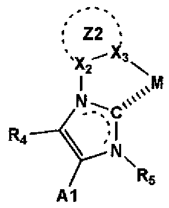
一般式 1

〔式中、 X、 Xは、各々炭素原子または窒素原子を表し、 R、 R、 R、 R、 R、 Rは、
2 3 2 3 4 5 6 7 各々水素原子または置換基を表し、 Z2は、 6員の芳香族炭化水素環を形成するの に必要な原子群または、 5員〜 6員の芳香族複素環を形成するのに必要な原子群を 表し、 Mは、 Irまたは Ptを表す。 A1は、溶解性調節基または製膜性調節基を有し、
該溶解性調節基または該製膜性調節基は、置換基を有する芳香族炭化水素基、置 換基を有する芳香族複素環基または、炭素数 6以上のアルキル基を表す。〕
[8] 前記溶解性調節基または製膜性調節基が、置換基を有する芳香族炭化水素環基ま たは置換基を有する芳香族複素環基であることを特徴とする請求の範囲第 1項〜請 求の範囲第 7項のいずれか 1項に記載の化合物。
[9] 前記溶解性調節基または製膜性調節基を少なくとも二つ有することを特徴とする請 求の範囲第 1項〜請求の範囲第 8項のいずれか 1項に記載の化合物。
[10] 前記溶解性調節基または製膜性調節基の式量が 115以上であることを特徴とする請 求の範囲第 1項〜請求の範囲第 9項のいずれか 1項に記載の化合物。
[11] 支持基板上に少なくとも陽極、陰極を有し、該陽極と該陰極間に少なくとも一層の発 光層を含む有機層を有する有機エレクト口ルミネッセンス素子において、
該有機層の少なくとも一層が、前記一般式(1)〜 (8)のいずれか 1項に記載の化合 物を含有することを特徴とする有機エレクト口ルミネッセンス素子。
[12] 支持基板上に少なくとも陽極、陰極を有し、該陽極と該陰極間に少なくとも一層の発 光層を含む有機層を有する有機エレクト口ルミネッセンス素子において、
該発光層の少なくとも一層が、前記一般式(1)〜(8)のいずれか 1項に記載の化合 物を含有することを特徴とする有機エレクト口ルミネッセンス素子。
[13] 前記発光層が塗布法により成膜されていることを特徴とする請求の範囲第 11項また は請求の範囲第 12項に記載の有機エレクト口ルミネッセンス素子。
[14] 請求の範囲第 11項〜請求の範囲第 13項のいずれか 1項に記載の有機エレクトロル ミネッセンス素子を具備することを特徴とする照明装置。
[15] 請求の範囲第 11項〜請求の範囲第 13項のいずれか 1項に記載の有機エレクトロル ミネッセンス素子を具備することを特徴とするディスプレイ装置。
Priority Applications (1)
| Application Number | Priority Date | Filing Date | Title |
|---|---|---|---|
| US12/297,594 US9005770B2 (en) | 2006-04-20 | 2007-04-17 | Compound, electroluminescent element containing the same, illuminating device and display device |
Applications Claiming Priority (2)
| Application Number | Priority Date | Filing Date | Title |
|---|---|---|---|
| JP2006116468A JP5103781B2 (ja) | 2006-04-20 | 2006-04-20 | 化合物、該化合物を含む有機エレクトロルミネッセンス素子、照明装置 |
| JP2006-116468 | 2006-04-20 |
Publications (1)
| Publication Number | Publication Date |
|---|---|
| WO2007123111A1 true WO2007123111A1 (ja) | 2007-11-01 |
Family
ID=38625011
Family Applications (1)
| Application Number | Title | Priority Date | Filing Date |
|---|---|---|---|
| PCT/JP2007/058324 Ceased WO2007123111A1 (ja) | 2006-04-20 | 2007-04-17 | 化合物、該化合物を含む有機エレクトロルミネッセンス素子、照明装置及びディスプレイ装置 |
Country Status (3)
| Country | Link |
|---|---|
| US (1) | US9005770B2 (ja) |
| JP (1) | JP5103781B2 (ja) |
| WO (1) | WO2007123111A1 (ja) |
Cited By (2)
| Publication number | Priority date | Publication date | Assignee | Title |
|---|---|---|---|---|
| JP2014055131A (ja) * | 2012-09-07 | 2014-03-27 | Samsung Display Co Ltd | 有機金属化合物およびそれを含んだ有機発光素子 |
| JP2015174824A (ja) * | 2014-03-13 | 2015-10-05 | 住友化学株式会社 | 金属錯体およびそれを用いた発光素子 |
Families Citing this family (19)
| Publication number | Priority date | Publication date | Assignee | Title |
|---|---|---|---|---|
| US7807839B2 (en) | 2005-10-18 | 2010-10-05 | Semiconductor Energy Laboratory Co., Ltd. | Organometallic complex, and light-emitting element and light-emitting device using the same |
| WO2008035571A1 (en) * | 2006-09-20 | 2008-03-27 | Konica Minolta Holdings, Inc. | Organic electroluminescence element |
| JP2010040512A (ja) * | 2008-07-10 | 2010-02-18 | Sumitomo Chemical Co Ltd | 有機エレクトロルミネッセンス素子およびその製造方法 |
| JP2010047734A (ja) * | 2008-08-25 | 2010-03-04 | Sony Corp | 有機el発光材料及び有機el発光素子 |
| JP2012006878A (ja) * | 2010-06-25 | 2012-01-12 | Mitsubishi Chemicals Corp | 有機金属錯体、発光材料、有機電界発光素子材料、有機金属錯体含有組成物、有機電界発光素子、有機elディスプレイおよび有機el照明 |
| JP2013010752A (ja) * | 2011-06-03 | 2013-01-17 | Semiconductor Energy Lab Co Ltd | 有機金属錯体、有機発光素子、発光装置、電子機器、及び照明装置 |
| JP2013073813A (ja) * | 2011-09-28 | 2013-04-22 | Toppan Printing Co Ltd | 有機エレクトロルミネッセンスパネルの製造方法 |
| JP5905270B2 (ja) * | 2012-01-18 | 2016-04-20 | 住友化学株式会社 | 金属錯体及び該金属錯体を含む発光素子 |
| JP5905271B2 (ja) * | 2012-01-18 | 2016-04-20 | 住友化学株式会社 | 金属錯体及び該金属錯体を含む発光素子 |
| US9929356B2 (en) * | 2012-11-30 | 2018-03-27 | Semiconductor Energy Laboratory Co., Ltd. | Light-emitting element, light-emitting device, electronic appliance, and lighting device |
| JP6134566B2 (ja) * | 2013-04-15 | 2017-05-24 | 住友化学株式会社 | 金属錯体及び該金属錯体を含む発光素子 |
| US9871205B2 (en) | 2013-08-02 | 2018-01-16 | Samsung Display Co., Ltd. | Organic light-emitting device |
| KR102086556B1 (ko) * | 2013-08-02 | 2020-03-10 | 삼성디스플레이 주식회사 | 유기 발광 소자 |
| JP2015044776A (ja) * | 2013-08-29 | 2015-03-12 | 国立大学法人山形大学 | イリジウム錯体及びそれを用いた有機エレクトロルミネッセンス素子 |
| US9478757B2 (en) * | 2014-02-26 | 2016-10-25 | E I Du Pont De Nemours And Company | Blue luminescent compounds |
| EP3131131B1 (en) * | 2014-04-09 | 2021-08-25 | Sumitomo Chemical Company Limited | Light-emission element, and composition used therein |
| US9843001B2 (en) * | 2014-08-18 | 2017-12-12 | E I Du Pont De Nemours And Company | Blue luminescent compounds |
| US10672996B2 (en) | 2015-09-03 | 2020-06-02 | Universal Display Corporation | Organic electroluminescent materials and devices |
| JP6646427B2 (ja) | 2015-12-15 | 2020-02-14 | 豊田鉄工株式会社 | 電池ケース |
Citations (3)
| Publication number | Priority date | Publication date | Assignee | Title |
|---|---|---|---|---|
| JP2005068110A (ja) * | 2003-08-27 | 2005-03-17 | Mitsubishi Chemicals Corp | 有機金属錯体、発光材料、および有機電界発光素子 |
| WO2007018067A1 (ja) * | 2005-08-05 | 2007-02-15 | Idemitsu Kosan Co., Ltd. | 遷移金属錯体化合物及びそれを用いた有機エレクトロルミネッセンス素子 |
| WO2007069542A1 (ja) * | 2005-12-15 | 2007-06-21 | Idemitsu Kosan Co., Ltd. | 遷移金属錯体化合物及びそれを用いた有機エレクトロルミネッセンス素子 |
Family Cites Families (8)
| Publication number | Priority date | Publication date | Assignee | Title |
|---|---|---|---|---|
| EP1366113B1 (en) | 2001-02-20 | 2011-04-13 | Isis Innovation Limited | Metal-containing dendrimers |
| JP4438042B2 (ja) * | 2001-03-08 | 2010-03-24 | キヤノン株式会社 | 金属配位化合物、電界発光素子及び表示装置 |
| JP4120271B2 (ja) | 2002-05-28 | 2008-07-16 | 日本化成株式会社 | [4−(ヒドロキシメチル)シクロヘキシル]メチルアクリレートの製造法 |
| US7338722B2 (en) * | 2003-03-24 | 2008-03-04 | The University Of Southern California | Phenyl and fluorenyl substituted phenyl-pyrazole complexes of Ir |
| GB0311234D0 (en) * | 2003-05-16 | 2003-06-18 | Isis Innovation | Organic phosphorescent material and organic optoelectronic device |
| JP4198654B2 (ja) * | 2003-08-07 | 2008-12-17 | 三星エスディアイ株式会社 | イリジウム化合物及びそれを採用した有機電界発光素子 |
| US7902374B2 (en) * | 2005-05-06 | 2011-03-08 | Universal Display Corporation | Stability OLED materials and devices |
| US9051344B2 (en) * | 2005-05-06 | 2015-06-09 | Universal Display Corporation | Stability OLED materials and devices |
-
2006
- 2006-04-20 JP JP2006116468A patent/JP5103781B2/ja not_active Expired - Fee Related
-
2007
- 2007-04-17 WO PCT/JP2007/058324 patent/WO2007123111A1/ja not_active Ceased
- 2007-04-17 US US12/297,594 patent/US9005770B2/en active Active
Patent Citations (3)
| Publication number | Priority date | Publication date | Assignee | Title |
|---|---|---|---|---|
| JP2005068110A (ja) * | 2003-08-27 | 2005-03-17 | Mitsubishi Chemicals Corp | 有機金属錯体、発光材料、および有機電界発光素子 |
| WO2007018067A1 (ja) * | 2005-08-05 | 2007-02-15 | Idemitsu Kosan Co., Ltd. | 遷移金属錯体化合物及びそれを用いた有機エレクトロルミネッセンス素子 |
| WO2007069542A1 (ja) * | 2005-12-15 | 2007-06-21 | Idemitsu Kosan Co., Ltd. | 遷移金属錯体化合物及びそれを用いた有機エレクトロルミネッセンス素子 |
Cited By (3)
| Publication number | Priority date | Publication date | Assignee | Title |
|---|---|---|---|---|
| JP2014055131A (ja) * | 2012-09-07 | 2014-03-27 | Samsung Display Co Ltd | 有機金属化合物およびそれを含んだ有機発光素子 |
| US9997728B2 (en) | 2012-09-07 | 2018-06-12 | Samsung Display Co., Ltd. | Organometallic compound and organic light-emitting device including the same |
| JP2015174824A (ja) * | 2014-03-13 | 2015-10-05 | 住友化学株式会社 | 金属錯体およびそれを用いた発光素子 |
Also Published As
| Publication number | Publication date |
|---|---|
| US9005770B2 (en) | 2015-04-14 |
| JP5103781B2 (ja) | 2012-12-19 |
| US20090102370A1 (en) | 2009-04-23 |
| JP2007284408A (ja) | 2007-11-01 |
Similar Documents
| Publication | Publication Date | Title |
|---|---|---|
| JP6119819B2 (ja) | 有機エレクトロルミネッセンス素子の製造方法 | |
| JP5157916B2 (ja) | 有機エレクトロルミネッセンス素子、表示装置及び照明装置 | |
| JP5790833B2 (ja) | 有機エレクトロルミネッセンス素子、表示装置及び照明装置 | |
| JP5458890B2 (ja) | 有機エレクトロルミネッセンス素子、表示装置及び照明装置 | |
| WO2007123111A1 (ja) | 化合物、該化合物を含む有機エレクトロルミネッセンス素子、照明装置及びディスプレイ装置 | |
| JP5887771B2 (ja) | 有機エレクトロルミネッセンス素子材料、有機エレクトロルミネッセンス素子、有機エレクトロルミネッセンス素子の製造方法、表示装置、照明装置、並びに化合物 | |
| JP5835061B2 (ja) | 有機エレクトロルミネッセンス素子、有機エレクトロルミネッセンス素子の製造方法、表示装置および照明装置 | |
| WO2007119816A1 (ja) | 有機エレクトロルミネッセンス素子材料、有機エレクトロルミネッセンス素子、表示装置及び照明装置 | |
| JP5900001B2 (ja) | 有機エレクトロルミネッセンス素子、それが具備された表示装置及び照明装置 | |
| WO2007077810A1 (ja) | 有機エレクトロルミネッセンス素子、表示装置及び照明装置 | |
| WO2007132886A1 (ja) | 有機エレクトロルミネッセンス素子材料、有機エレクトロルミネッセンス素子、表示装置及び照明装置 | |
| WO2008072596A1 (ja) | 有機エレクトロルミネッセンス素子、表示装置及び照明装置 | |
| JP5692011B2 (ja) | 有機エレクトロルミネッセンス素子材料、有機エレクトロルミネッセンス素子、表示装置、並びに照明装置 | |
| JP5783290B2 (ja) | 有機エレクトロルミネッセンス素子材料 | |
| JP5625750B2 (ja) | 有機エレクトロルミネッセンス素子材料、有機エレクトロルミネッセンス素子とその製造方法、表示装置及び照明装置 | |
| JP5560517B2 (ja) | 有機エレクトロルミネッセンス素子、表示装置及び照明装置 | |
| JP5741373B2 (ja) | 有機エレクトロルミネッセンス素子材料、有機エレクトロルミネッセンス素子、表示装置、並びに照明装置 | |
| WO2007029461A1 (ja) | 有機エレクトロルミネッセンス素子、その製造方法、該有機エレクトロルミネッセンス素子を有する表示装置及び照明装置 | |
| JP5720253B2 (ja) | 有機エレクトロニクス素子、それを具備した表示装置及び照明装置 | |
| WO2007043321A1 (ja) | 有機エレクトロルミネッセンス素子、液晶表示装置及び照明装置 | |
| JP6070756B2 (ja) | 有機エレクトロルミネッセンス素子材料、有機エレクトロルミネッセンス素子、有機エレクトロルミネッセンス素子の製造方法、表示装置、並びに照明装置 | |
| JP5532563B2 (ja) | 有機エレクトロルミネッセンス素子材料、有機エレクトロルミネッセンス素子、表示装置及び照明装置 | |
| JP6156521B2 (ja) | 有機エレクトロニクス素子、表示装置及び照明装置 | |
| JP2016048796A (ja) | 有機エレクトロルミネッセンス素子、それが具備された表示装置及び照明装置 |
Legal Events
| Date | Code | Title | Description |
|---|---|---|---|
| 121 | Ep: the epo has been informed by wipo that ep was designated in this application |
Ref document number: 07741760 Country of ref document: EP Kind code of ref document: A1 |
|
| WWE | Wipo information: entry into national phase |
Ref document number: 12297594 Country of ref document: US |
|
| NENP | Non-entry into the national phase |
Ref country code: DE |
|
| 122 | Ep: pct application non-entry in european phase |
Ref document number: 07741760 Country of ref document: EP Kind code of ref document: A1 |