WO2009081775A1 - Procédé de fabrication de transistor à couches minces et transistor à couches minces - Google Patents
Procédé de fabrication de transistor à couches minces et transistor à couches minces Download PDFInfo
- Publication number
- WO2009081775A1 WO2009081775A1 PCT/JP2008/072685 JP2008072685W WO2009081775A1 WO 2009081775 A1 WO2009081775 A1 WO 2009081775A1 JP 2008072685 W JP2008072685 W JP 2008072685W WO 2009081775 A1 WO2009081775 A1 WO 2009081775A1
- Authority
- WO
- WIPO (PCT)
- Prior art keywords
- film
- amorphous silicon
- laser
- thin
- film transistor
- Prior art date
- Legal status (The legal status is an assumption and is not a legal conclusion. Google has not performed a legal analysis and makes no representation as to the accuracy of the status listed.)
- Ceased
Links
Images

Classifications
-
- H—ELECTRICITY
- H10—SEMICONDUCTOR DEVICES; ELECTRIC SOLID-STATE DEVICES NOT OTHERWISE PROVIDED FOR
- H10D—INORGANIC ELECTRIC SEMICONDUCTOR DEVICES
- H10D30/00—Field-effect transistors [FET]
- H10D30/01—Manufacture or treatment
- H10D30/021—Manufacture or treatment of FETs having insulated gates [IGFET]
- H10D30/031—Manufacture or treatment of FETs having insulated gates [IGFET] of thin-film transistors [TFT]
- H10D30/0312—Manufacture or treatment of FETs having insulated gates [IGFET] of thin-film transistors [TFT] characterised by the gate electrodes
- H10D30/0316—Manufacture or treatment of FETs having insulated gates [IGFET] of thin-film transistors [TFT] characterised by the gate electrodes of lateral bottom-gate TFTs comprising only a single gate
-
- H—ELECTRICITY
- H10—SEMICONDUCTOR DEVICES; ELECTRIC SOLID-STATE DEVICES NOT OTHERWISE PROVIDED FOR
- H10P—GENERIC PROCESSES OR APPARATUS FOR THE MANUFACTURE OR TREATMENT OF DEVICES COVERED BY CLASS H10
- H10P14/00—Formation of materials, e.g. in the shape of layers or pillars
- H10P14/20—Formation of materials, e.g. in the shape of layers or pillars of semiconductor materials
- H10P14/34—Deposited materials, e.g. layers
- H10P14/3402—Deposited materials, e.g. layers characterised by the chemical composition
- H10P14/3404—Deposited materials, e.g. layers characterised by the chemical composition being Group IVA materials
- H10P14/3411—Silicon, silicon germanium or germanium
-
- H—ELECTRICITY
- H10—SEMICONDUCTOR DEVICES; ELECTRIC SOLID-STATE DEVICES NOT OTHERWISE PROVIDED FOR
- H10D—INORGANIC ELECTRIC SEMICONDUCTOR DEVICES
- H10D30/00—Field-effect transistors [FET]
- H10D30/01—Manufacture or treatment
- H10D30/021—Manufacture or treatment of FETs having insulated gates [IGFET]
- H10D30/031—Manufacture or treatment of FETs having insulated gates [IGFET] of thin-film transistors [TFT]
- H10D30/0321—Manufacture or treatment of FETs having insulated gates [IGFET] of thin-film transistors [TFT] comprising silicon, e.g. amorphous silicon or polysilicon
-
- H—ELECTRICITY
- H10—SEMICONDUCTOR DEVICES; ELECTRIC SOLID-STATE DEVICES NOT OTHERWISE PROVIDED FOR
- H10D—INORGANIC ELECTRIC SEMICONDUCTOR DEVICES
- H10D30/00—Field-effect transistors [FET]
- H10D30/60—Insulated-gate field-effect transistors [IGFET]
- H10D30/67—Thin-film transistors [TFT]
- H10D30/674—Thin-film transistors [TFT] characterised by the active materials
-
- H—ELECTRICITY
- H10—SEMICONDUCTOR DEVICES; ELECTRIC SOLID-STATE DEVICES NOT OTHERWISE PROVIDED FOR
- H10D—INORGANIC ELECTRIC SEMICONDUCTOR DEVICES
- H10D62/00—Semiconductor bodies, or regions thereof, of devices having potential barriers
- H10D62/40—Crystalline structures
-
- H—ELECTRICITY
- H10—SEMICONDUCTOR DEVICES; ELECTRIC SOLID-STATE DEVICES NOT OTHERWISE PROVIDED FOR
- H10D—INORGANIC ELECTRIC SEMICONDUCTOR DEVICES
- H10D86/00—Integrated devices formed in or on insulating or conducting substrates, e.g. formed in silicon-on-insulator [SOI] substrates or on stainless steel or glass substrates
- H10D86/40—Integrated devices formed in or on insulating or conducting substrates, e.g. formed in silicon-on-insulator [SOI] substrates or on stainless steel or glass substrates characterised by multiple TFTs
-
- H—ELECTRICITY
- H10—SEMICONDUCTOR DEVICES; ELECTRIC SOLID-STATE DEVICES NOT OTHERWISE PROVIDED FOR
- H10P—GENERIC PROCESSES OR APPARATUS FOR THE MANUFACTURE OR TREATMENT OF DEVICES COVERED BY CLASS H10
- H10P14/00—Formation of materials, e.g. in the shape of layers or pillars
- H10P14/20—Formation of materials, e.g. in the shape of layers or pillars of semiconductor materials
- H10P14/29—Formation of materials, e.g. in the shape of layers or pillars of semiconductor materials characterised by the substrates
- H10P14/2901—Materials
- H10P14/2922—Materials being non-crystalline insulating materials, e.g. glass or polymers
-
- H—ELECTRICITY
- H10—SEMICONDUCTOR DEVICES; ELECTRIC SOLID-STATE DEVICES NOT OTHERWISE PROVIDED FOR
- H10P—GENERIC PROCESSES OR APPARATUS FOR THE MANUFACTURE OR TREATMENT OF DEVICES COVERED BY CLASS H10
- H10P14/00—Formation of materials, e.g. in the shape of layers or pillars
- H10P14/20—Formation of materials, e.g. in the shape of layers or pillars of semiconductor materials
- H10P14/38—Formation of materials, e.g. in the shape of layers or pillars of semiconductor materials characterised by treatments done after the formation of the materials
- H10P14/3802—Crystallisation or recrystallisation of non-monocrystalline semiconductor materials, e.g. regrowth
- H10P14/3808—Crystallisation or recrystallisation of non-monocrystalline semiconductor materials, e.g. regrowth using laser beams
-
- H—ELECTRICITY
- H10—SEMICONDUCTOR DEVICES; ELECTRIC SOLID-STATE DEVICES NOT OTHERWISE PROVIDED FOR
- H10D—INORGANIC ELECTRIC SEMICONDUCTOR DEVICES
- H10D30/00—Field-effect transistors [FET]
- H10D30/60—Insulated-gate field-effect transistors [IGFET]
- H10D30/67—Thin-film transistors [TFT]
- H10D30/6757—Thin-film transistors [TFT] characterised by the structure of the channel, e.g. transverse or longitudinal shape or doping profile
-
- H—ELECTRICITY
- H10—SEMICONDUCTOR DEVICES; ELECTRIC SOLID-STATE DEVICES NOT OTHERWISE PROVIDED FOR
- H10D—INORGANIC ELECTRIC SEMICONDUCTOR DEVICES
- H10D86/00—Integrated devices formed in or on insulating or conducting substrates, e.g. formed in silicon-on-insulator [SOI] substrates or on stainless steel or glass substrates
- H10D86/01—Manufacture or treatment
- H10D86/021—Manufacture or treatment of multiple TFTs
- H10D86/0221—Manufacture or treatment of multiple TFTs comprising manufacture, treatment or patterning of TFT semiconductor bodies
- H10D86/0223—Manufacture or treatment of multiple TFTs comprising manufacture, treatment or patterning of TFT semiconductor bodies comprising crystallisation of amorphous, microcrystalline or polycrystalline semiconductor materials
- H10D86/0229—Manufacture or treatment of multiple TFTs comprising manufacture, treatment or patterning of TFT semiconductor bodies comprising crystallisation of amorphous, microcrystalline or polycrystalline semiconductor materials characterised by control of the annealing or irradiation parameters
Definitions
- the solid green laser may be a continuous laser or a pulsed laser.
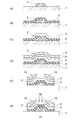
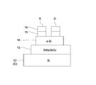
- the source electrode film and the drain electrode film function as a laser mask. Therefore, only the channel portion of the amorphous silicon film can be selectively annealed by spot irradiation or scanning irradiation of a solid green laser.
- a gate electrode film 2 is formed on the surface of a substrate 1.
- the gate insulating film 3 is formed of a silicon nitride film (SiNx), a silicon oxide film (SiO 2 ), or the like, and is formed by, for example, a CVD method.
- the thickness of the gate insulating film 3 is, for example, 200 nm to 500 nm.
- an ohmic contact layer 5 and an electrode layer 6 are sequentially laminated on the amorphous silicon film 4.
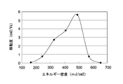
- a region of the amorphous silicon film 14 (channel portion) located between the source electrode film S and the drain electrode film D is irradiated with a solid green laser, and then a heat treatment (annealing) in a hydrogen atmosphere is performed. 30 minutes at a temperature. It has been confirmed that the heat treatment (annealing) in the hydrogen atmosphere shows a higher mobility improvement effect as the treatment is performed at a higher temperature.
- a preferable heat treatment temperature is 400 ° C. or higher.
- scanning annealing of a solid green laser has been described as an example for laser annealing to the amorphous silicon film 4 (channel portion 41).
- the same effects as described above can also be obtained by spot irradiation.
Landscapes
- Recrystallisation Techniques (AREA)
- Thin Film Transistor (AREA)
Abstract
Priority Applications (5)
| Application Number | Priority Date | Filing Date | Title |
|---|---|---|---|
| JP2009547039A JP4856252B2 (ja) | 2007-12-25 | 2008-12-12 | 薄膜トランジスタの製造方法 |
| DE112008003488T DE112008003488B4 (de) | 2007-12-25 | 2008-12-12 | Verfahren zum Herstellen eines Dünnschichttransistors und Dünnschichttransistor |
| KR1020107014518A KR101133827B1 (ko) | 2007-12-25 | 2008-12-12 | 박막 트랜지스터의 제조 방법 및 박막 트랜지스터 |
| CN2008801227994A CN101939829B (zh) | 2007-12-25 | 2008-12-12 | 薄膜晶体管制造方法以及薄膜晶体管 |
| US12/808,397 US8673705B2 (en) | 2007-12-25 | 2008-12-12 | Method of producing thin film transistor and thin film transistor |
Applications Claiming Priority (2)
| Application Number | Priority Date | Filing Date | Title |
|---|---|---|---|
| JP2007332774 | 2007-12-25 | ||
| JP2007-332774 | 2007-12-25 |
Publications (1)
| Publication Number | Publication Date |
|---|---|
| WO2009081775A1 true WO2009081775A1 (fr) | 2009-07-02 |
Family
ID=40801081
Family Applications (1)
| Application Number | Title | Priority Date | Filing Date |
|---|---|---|---|
| PCT/JP2008/072685 Ceased WO2009081775A1 (fr) | 2007-12-25 | 2008-12-12 | Procédé de fabrication de transistor à couches minces et transistor à couches minces |
Country Status (7)
| Country | Link |
|---|---|
| US (1) | US8673705B2 (fr) |
| JP (1) | JP4856252B2 (fr) |
| KR (1) | KR101133827B1 (fr) |
| CN (1) | CN101939829B (fr) |
| DE (1) | DE112008003488B4 (fr) |
| TW (1) | TW200939357A (fr) |
| WO (1) | WO2009081775A1 (fr) |
Cited By (1)
| Publication number | Priority date | Publication date | Assignee | Title |
|---|---|---|---|---|
| US10818492B2 (en) | 2016-03-16 | 2020-10-27 | V Technology Co., Ltd. | Method for manufacturing thin film transistor and mask for use in the manufacturing method |
Families Citing this family (6)
| Publication number | Priority date | Publication date | Assignee | Title |
|---|---|---|---|---|
| CN103493186A (zh) * | 2011-11-29 | 2014-01-01 | 松下电器产业株式会社 | 薄膜晶体管阵列的制造方法、薄膜晶体管阵列及显示装置 |
| US20190140102A1 (en) * | 2016-04-25 | 2019-05-09 | Sakai Display Products Corporation | Thin film transistor, display device, and thin film transistor manufacturing method |
| CN108735819B (zh) * | 2017-04-13 | 2020-07-14 | 京东方科技集团股份有限公司 | 低温多晶硅薄膜晶体管及其制造方法、显示基板 |
| JP7335236B2 (ja) * | 2017-10-13 | 2023-08-29 | ザ トラスティーズ オブ コロンビア ユニヴァーシティ イン ザ シティ オブ ニューヨーク | スポットビーム及びラインビーム結晶化のためのシステムおよび方法 |
| CN113611752B (zh) * | 2021-07-19 | 2024-01-16 | Tcl华星光电技术有限公司 | 低温多晶硅tft的制作方法及低温多晶硅tft |
| KR102866351B1 (ko) * | 2021-11-23 | 2025-10-01 | 한국과학기술원 | 비정질 실리콘의 재결정화 방법 및 이를 이용한 반도체 소자의 게이트 형성방법 |
Citations (6)
| Publication number | Priority date | Publication date | Assignee | Title |
|---|---|---|---|---|
| JPS60245124A (ja) * | 1984-05-18 | 1985-12-04 | Sony Corp | 半導体装置の製法 |
| JPH0362971A (ja) * | 1989-07-31 | 1991-03-19 | Sanyo Electric Co Ltd | 薄膜トランジスタ |
| JPH04186735A (ja) * | 1990-11-20 | 1992-07-03 | Matsushita Electric Ind Co Ltd | 半導体装置の製造方法 |
| JP2002094078A (ja) * | 2000-06-28 | 2002-03-29 | Semiconductor Energy Lab Co Ltd | 半導体装置 |
| JP2007035964A (ja) * | 2005-07-27 | 2007-02-08 | Sony Corp | 薄膜トランジスタとその製造方法、及び表示装置 |
| JP2007220918A (ja) * | 2006-02-16 | 2007-08-30 | Ulvac Japan Ltd | レーザアニール方法、薄膜半導体装置及びその製造方法、並びに表示装置及びその製造方法 |
Family Cites Families (8)
| Publication number | Priority date | Publication date | Assignee | Title |
|---|---|---|---|---|
| US4459739A (en) * | 1981-05-26 | 1984-07-17 | Northern Telecom Limited | Thin film transistors |
| JP3255942B2 (ja) * | 1991-06-19 | 2002-02-12 | 株式会社半導体エネルギー研究所 | 逆スタガ薄膜トランジスタの作製方法 |
| JPH1056180A (ja) * | 1995-09-29 | 1998-02-24 | Canon Inc | 半導体装置及びその製造方法 |
| TW504846B (en) * | 2000-06-28 | 2002-10-01 | Semiconductor Energy Lab | Semiconductor device and manufacturing method thereof |
| JP4030758B2 (ja) * | 2001-12-28 | 2008-01-09 | 株式会社半導体エネルギー研究所 | 半導体装置の作製方法 |
| TWI267131B (en) * | 2002-03-05 | 2006-11-21 | Semiconductor Energy Lab | Semiconductor element and semiconductor device using the same |
| CN100367479C (zh) * | 2005-02-06 | 2008-02-06 | 友达光电股份有限公司 | 一种薄膜晶体管的制造方法 |
| KR100785020B1 (ko) * | 2006-06-09 | 2007-12-12 | 삼성전자주식회사 | 하부 게이트 박막 트랜지스터 및 그 제조방법 |
-
2008
- 2008-12-12 WO PCT/JP2008/072685 patent/WO2009081775A1/fr not_active Ceased
- 2008-12-12 JP JP2009547039A patent/JP4856252B2/ja not_active Expired - Fee Related
- 2008-12-12 US US12/808,397 patent/US8673705B2/en not_active Expired - Fee Related
- 2008-12-12 CN CN2008801227994A patent/CN101939829B/zh not_active Expired - Fee Related
- 2008-12-12 DE DE112008003488T patent/DE112008003488B4/de active Active
- 2008-12-12 KR KR1020107014518A patent/KR101133827B1/ko active Active
- 2008-12-23 TW TW097150186A patent/TW200939357A/zh unknown
Patent Citations (6)
| Publication number | Priority date | Publication date | Assignee | Title |
|---|---|---|---|---|
| JPS60245124A (ja) * | 1984-05-18 | 1985-12-04 | Sony Corp | 半導体装置の製法 |
| JPH0362971A (ja) * | 1989-07-31 | 1991-03-19 | Sanyo Electric Co Ltd | 薄膜トランジスタ |
| JPH04186735A (ja) * | 1990-11-20 | 1992-07-03 | Matsushita Electric Ind Co Ltd | 半導体装置の製造方法 |
| JP2002094078A (ja) * | 2000-06-28 | 2002-03-29 | Semiconductor Energy Lab Co Ltd | 半導体装置 |
| JP2007035964A (ja) * | 2005-07-27 | 2007-02-08 | Sony Corp | 薄膜トランジスタとその製造方法、及び表示装置 |
| JP2007220918A (ja) * | 2006-02-16 | 2007-08-30 | Ulvac Japan Ltd | レーザアニール方法、薄膜半導体装置及びその製造方法、並びに表示装置及びその製造方法 |
Cited By (1)
| Publication number | Priority date | Publication date | Assignee | Title |
|---|---|---|---|---|
| US10818492B2 (en) | 2016-03-16 | 2020-10-27 | V Technology Co., Ltd. | Method for manufacturing thin film transistor and mask for use in the manufacturing method |
Also Published As
| Publication number | Publication date |
|---|---|
| TW200939357A (en) | 2009-09-16 |
| JPWO2009081775A1 (ja) | 2011-05-06 |
| US20100301339A1 (en) | 2010-12-02 |
| JP4856252B2 (ja) | 2012-01-18 |
| CN101939829B (zh) | 2013-03-27 |
| CN101939829A (zh) | 2011-01-05 |
| US8673705B2 (en) | 2014-03-18 |
| KR101133827B1 (ko) | 2012-04-06 |
| DE112008003488B4 (de) | 2012-01-19 |
| DE112008003488T5 (de) | 2010-10-21 |
| KR20100089895A (ko) | 2010-08-12 |
Similar Documents
| Publication | Publication Date | Title |
|---|---|---|
| US7323368B2 (en) | Method for manufacturing semiconductor device and heat treatment method | |
| JP3586558B2 (ja) | 薄膜の改質方法及びその実施に使用する装置 | |
| JP4856252B2 (ja) | 薄膜トランジスタの製造方法 | |
| KR101015844B1 (ko) | 박막트랜지스터, 그의 제조방법 및 그를 구비하는유기전계발광표시장치의 제조방법 | |
| JPH0794756A (ja) | 半導体装置の作製方法 | |
| JPH06124890A (ja) | 薄膜状半導体装置の作製方法。 | |
| JP2005064453A (ja) | 薄膜トランジスタ及びその製造方法 | |
| JPH0917729A (ja) | 半導体装置の製造方法 | |
| JP2009147256A (ja) | ディスプレーデバイス用半導体装置の製造方法 | |
| JP2004039660A (ja) | 多結晶半導体膜の製造方法、薄膜トランジスタの製造方法、表示装置、およびパルスレーザアニール装置 | |
| JP3844537B2 (ja) | 多結晶半導体膜の製造方法 | |
| JP2007220918A (ja) | レーザアニール方法、薄膜半導体装置及びその製造方法、並びに表示装置及びその製造方法 | |
| JP4239744B2 (ja) | 薄膜トランジスタの製造方法 | |
| JP2007035812A (ja) | 多結晶シリコン膜の製造方法および薄膜トランジスタ | |
| JP2001057432A (ja) | 薄膜素子の転写方法 | |
| JP2002280304A (ja) | 半導体装置の製造方法 | |
| JP3925085B2 (ja) | 半導体装置の製造方法、光変調素子の製造方法、および表示装置の製造方法 | |
| KR100796607B1 (ko) | 다결정 실리콘 결정화방법과 그를 이용한 박막트랜지스터의 제조 방법 | |
| JP3462157B2 (ja) | 半導体装置の作製方法 | |
| JPH06124889A (ja) | 薄膜状半導体装置の作製方法 | |
| JPH09237767A (ja) | 半導体装置の製造方法 | |
| JP4271453B2 (ja) | 半導体結晶化方法および薄膜トランジスタの製造方法 | |
| JPH11330477A (ja) | 薄膜トランジスタの製造方法 | |
| WO2010024278A1 (fr) | Procédé de fabrication d'un transistor à film mince, et transistor à film mince | |
| JP3684909B2 (ja) | 薄膜トランジスタ作成方法 |
Legal Events
| Date | Code | Title | Description |
|---|---|---|---|
| WWE | Wipo information: entry into national phase |
Ref document number: 200880122799.4 Country of ref document: CN |
|
| 121 | Ep: the epo has been informed by wipo that ep was designated in this application |
Ref document number: 08864176 Country of ref document: EP Kind code of ref document: A1 |
|
| ENP | Entry into the national phase |
Ref document number: 2009547039 Country of ref document: JP Kind code of ref document: A |
|
| WWE | Wipo information: entry into national phase |
Ref document number: 1120080034885 Country of ref document: DE |
|
| ENP | Entry into the national phase |
Ref document number: 20107014518 Country of ref document: KR Kind code of ref document: A |
|
| WWE | Wipo information: entry into national phase |
Ref document number: 12808397 Country of ref document: US |
|
| RET | De translation (de og part 6b) |
Ref document number: 112008003488 Country of ref document: DE Date of ref document: 20101021 Kind code of ref document: P |
|
| REG | Reference to national code |
Ref country code: DE Ref legal event code: 8607 |
|
| REG | Reference to national code |
Ref country code: DE Ref legal event code: 8607 |
|
| 122 | Ep: pct application non-entry in european phase |
Ref document number: 08864176 Country of ref document: EP Kind code of ref document: A1 |