WO2009081980A1 - 発光装置 - Google Patents
発光装置 Download PDFInfo
- Publication number
- WO2009081980A1 WO2009081980A1 PCT/JP2008/073591 JP2008073591W WO2009081980A1 WO 2009081980 A1 WO2009081980 A1 WO 2009081980A1 JP 2008073591 W JP2008073591 W JP 2008073591W WO 2009081980 A1 WO2009081980 A1 WO 2009081980A1
- Authority
- WO
- WIPO (PCT)
- Prior art keywords
- light emitting
- emitting device
- light
- base
- emitting element
- Prior art date
- Legal status (The legal status is an assumption and is not a legal conclusion. Google has not performed a legal analysis and makes no representation as to the accuracy of the status listed.)
- Ceased
Links
Images


Classifications
-
- H—ELECTRICITY
- H10—SEMICONDUCTOR DEVICES; ELECTRIC SOLID-STATE DEVICES NOT OTHERWISE PROVIDED FOR
- H10H—INORGANIC LIGHT-EMITTING SEMICONDUCTOR DEVICES HAVING POTENTIAL BARRIERS
- H10H20/00—Individual inorganic light-emitting semiconductor devices having potential barriers, e.g. light-emitting diodes [LED]
- H10H20/80—Constructional details
- H10H20/85—Packages
- H10H20/855—Optical field-shaping means, e.g. lenses
- H10H20/856—Reflecting means
-
- H—ELECTRICITY
- H10—SEMICONDUCTOR DEVICES; ELECTRIC SOLID-STATE DEVICES NOT OTHERWISE PROVIDED FOR
- H10H—INORGANIC LIGHT-EMITTING SEMICONDUCTOR DEVICES HAVING POTENTIAL BARRIERS
- H10H20/00—Individual inorganic light-emitting semiconductor devices having potential barriers, e.g. light-emitting diodes [LED]
- H10H20/80—Constructional details
- H10H20/85—Packages
- H10H20/851—Wavelength conversion means
- H10H20/8515—Wavelength conversion means not being in contact with the bodies
-
- H—ELECTRICITY
- H10—SEMICONDUCTOR DEVICES; ELECTRIC SOLID-STATE DEVICES NOT OTHERWISE PROVIDED FOR
- H10H—INORGANIC LIGHT-EMITTING SEMICONDUCTOR DEVICES HAVING POTENTIAL BARRIERS
- H10H20/00—Individual inorganic light-emitting semiconductor devices having potential barriers, e.g. light-emitting diodes [LED]
- H10H20/80—Constructional details
- H10H20/85—Packages
- H10H20/852—Encapsulations
- H10H20/853—Encapsulations characterised by their shape
-
- H—ELECTRICITY
- H10—SEMICONDUCTOR DEVICES; ELECTRIC SOLID-STATE DEVICES NOT OTHERWISE PROVIDED FOR
- H10H—INORGANIC LIGHT-EMITTING SEMICONDUCTOR DEVICES HAVING POTENTIAL BARRIERS
- H10H20/00—Individual inorganic light-emitting semiconductor devices having potential barriers, e.g. light-emitting diodes [LED]
- H10H20/80—Constructional details
- H10H20/85—Packages
- H10H20/858—Means for heat extraction or cooling
- H10H20/8582—Means for heat extraction or cooling characterised by their shape
-
- H—ELECTRICITY
- H10—SEMICONDUCTOR DEVICES; ELECTRIC SOLID-STATE DEVICES NOT OTHERWISE PROVIDED FOR
- H10W—GENERIC PACKAGES, INTERCONNECTIONS, CONNECTORS OR OTHER CONSTRUCTIONAL DETAILS OF DEVICES COVERED BY CLASS H10
- H10W72/00—Interconnections or connectors in packages
- H10W72/20—Bump connectors, e.g. solder bumps or copper pillars; Dummy bumps; Thermal bumps
-
- H—ELECTRICITY
- H10—SEMICONDUCTOR DEVICES; ELECTRIC SOLID-STATE DEVICES NOT OTHERWISE PROVIDED FOR
- H10W—GENERIC PACKAGES, INTERCONNECTIONS, CONNECTORS OR OTHER CONSTRUCTIONAL DETAILS OF DEVICES COVERED BY CLASS H10
- H10W90/00—Package configurations
- H10W90/701—Package configurations characterised by the relative positions of pads or connectors relative to package parts
- H10W90/721—Package configurations characterised by the relative positions of pads or connectors relative to package parts of bump connectors
- H10W90/724—Package configurations characterised by the relative positions of pads or connectors relative to package parts of bump connectors between a chip and a stacked insulating package substrate, interposer or RDL
Definitions
- the present invention relates to a light emitting device having a light emitting element such as a light emitting diode.
- a light emitting device having a light emitting element such as a light emitting diode has been developed.
- a light emitting device having a light emitting element is expected from the viewpoint of, for example, power consumption or product life.
- a light emitting device having a light emitting element is required to be further improved with respect to light emission characteristics such as light emission intensity.
- the base has an upper portion including a first portion and a second portion.
- the first portion includes a mounting region for the light emitting element and has a first porosity.
- the second portion surrounds the first portion, includes a plurality of translucent particles, and has a second porosity that is greater than the first porosity.
- the translucent layer encapsulates the light emitting element and adheres to the first portion in a state of being separated from the second portion.
- FIG. 1 illustrates the concept of the present invention.
- the top view in the line of sight 100 of FIG. 1 is shown.
- the structure of the 2nd part shown by FIG. 1 and FIG. 2 is shown.
- 1 shows a light emitting device in one embodiment of the present invention.
- 5 shows a cross-sectional view of the light emitting device shown in FIG. 3 shows the substrate 2 shown in FIGS. 1 and 2.
- 4 shows a mounting structure of the light-emitting element 1 shown in FIGS. 6 shows an exemplary method for manufacturing the light emitting device shown in FIGS. 4 and 5.
- FIG. 9 shows the structure obtained in step 806 shown in FIG.
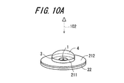
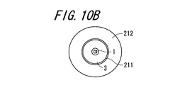
- FIG. 9B shows a plan view at line of sight 102 of FIG.
- FIG. 9 shows the structure obtained in step 806 shown in FIG. 10B is a plan view taken along line of sight 102 in FIG. 10A.
- 3 shows a light emitting device according to another embodiment of the present invention.
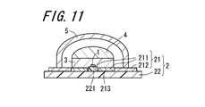
- the submount substrate 221 shown in FIG. 11 is shown.
- 3 shows a light emitting device according to another embodiment of the present invention.
- 3 shows a light emitting device according to another embodiment of the present invention.
- 3 shows a light emitting device according to another embodiment of the present invention.
- 3 shows a light emitting device according to another embodiment of the present invention.
- 3 shows a light emitting device according to another embodiment of the present invention.
- 3 shows a light emitting device according to another embodiment of the present invention.
- 3 shows a light emitting device according to another embodiment of the present invention.
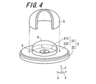
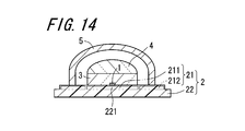
- the light emitting device includes a light emitting element 1, a base 2, and a translucent layer 3.
- the light emitting element 1 is mounted on the base 2.
- the exemplary light emitting device 1 is a light emitting diode containing a semiconductor material.
- the light emitting element 1 emits primary light according to the driving power.
- the base body 2 has an upper portion 21 including a first portion 211 and a second portion 212.
- the first portion 211 has a first porosity.
- the second part 212 surrounds the first part 211.
- the second portion 212 includes a plurality of translucent particles and has a second porosity that is greater than the first porosity.
- the structure of the second portion 212 will be described with reference to FIG.
- the plurality of translucent particles 401 are partially integrated.
- a plurality of cells 402 are present between the plurality of translucent particles 401.
- the translucent particle 401 has a higher refractive index than the cell 402.
- the primary light 10 emitted from the light emitting element 1 is incident on the translucent particles 401.
- the interface 403 between the translucent particle 401 and the cell 402 reflects the primary light 10 incident on the translucent particle 401 by total reflection.
- the interface 403 reflects the primary light 10 by total reflection.
- the critical angle ⁇ 403 is expressed by the following equation.
- the translucent layer 3 is attached to the first portion in a state of being separated from the second portion.
- the “separation” means that a distance 32 exists between the translucent layer 3 and the second portion 212 as shown in FIG.
- the light transmissive layer 3 encloses the light emitting element 1.
- the light emitting device in one embodiment of the present invention includes a light emitting element 1, a base 2, and a translucent layer 3.
- the light emitting device further includes a lens 4 and a wavelength conversion member 5.
- the wavelength conversion member 5 is partially omitted.
- the light emitting device is mounted on an xy plane in a virtual xyz space.
- the upward direction means the positive direction of the virtual z axis.
- the light emitting element 1 is mounted on the base 2.
- the exemplary light emitting device 1 is a light emitting diode containing a semiconductor material.
- the light emitting element 1 emits primary light according to the driving power.
- the primary light has a peak emission wavelength included in the range from 395 nm to 410 nm.
- the base body 2 has an upper portion 21 including a first portion 211 and a second portion 212.
- the base 2 includes a sub-base 22 having a protrusion 221.
- the mounting region of the light emitting element 1 is provided on the upper surface of the protruding portion 221.
- the first portion 211 includes an annular member 213 and a protruding portion 221.
- the light emitting device of this embodiment has an improvement in overall strength by having the sub-base including the protrusion 221. Therefore, the light emitting device is improved with respect to light emission characteristics such as light emission distribution.
- the exemplary annular member 213 has a ring shape. In FIG. 6, the substrate 2 is shown in a disassembled state.
- the annular member 213 is provided on the sub-base 22 and surrounds the protruding portion 221 of the sub-base 22.
- the annular member 213 is substantially made of ceramics.
- the annular member 213 has a first porosity included in a range from 0.001% to 1%.
- An exemplary method for measuring the porosity of the annular member 213 in this embodiment is a mercury intrusion method using a Pore Sizer 9310 model manufactured by Micromeritics.
- the exemplary second portion 212 has a ring shape.
- the second portion 212 is provided on the sub-base 22 and surrounds the first portion 211.
- the second portion 212 includes a plurality of translucent particles.
- the plurality of translucent particles are partially integrated. A plurality of cells exist between the plurality of translucent particles.
- the second portion 212 is formed in a porous shape.
- the second portion 212 has a second porosity included in the range of 15% to 43%.
- An exemplary method for measuring the porosity of the second portion 212 in this embodiment is a mercury intrusion method using a Pore Sizer 9310 model manufactured by Micromeritics.
- the second porosity is greater than the first porosity.
- the exemplary second portion 212 consists essentially of ceramics.
- the exemplary sub-substrate 22 is substantially made of ceramic.
- the sub-base 22 has a porosity included in a range from 0.001% to 1%.
- the method for measuring the porosity of the sub-substrate 22 in this embodiment is a mercury intrusion method using a pore sizer 9310 manufactured by Micromeritics.
- the sub-base 22 has a plurality of electrical paths 222.
- the light emitting element 1 is electrically connected to the plurality of electrical paths 222 via a conductive bonding material.
- the light emitting element 1 is mounted on the protruding portion 221 of the sub-base 22 by flip chip connection.
- the translucent layer 3 is provided on the base 2. The translucent layer 3 is attached to the first portion 211 in a state of being separated from the second portion 212 and encapsulates the light emitting element 1. “Translucent” of the layer 3 means that at least a part of the primary light emitted from the light emitting element 1 can be transmitted.
- the exemplary translucent layer 3 is substantially made of a silicone resin.
- the translucent layer 3 is attached to the upper surface of the first portion 211.
- the lens 4 is provided on the translucent layer 3.
- the lens 4 has translucency.
- the translucency of the lens 4 means that at least part of the primary light emitted from the light emitting element 1 can be transmitted.
- the exemplary lens 4 consists essentially of a glass material.
- the wavelength conversion member 5 is provided on the base 2.
- the wavelength conversion member 5 covers the light emitting element 1, the translucent layer 3, and the lens 4 through a gap.
- the wavelength conversion member 5 has a dome shape.
- the wavelength conversion member 5 emits secondary light according to the primary light emitted from the light emitting element 1.
- the wavelength conversion member 5 includes a matrix member and a plurality of fluorescent particles.
- the matrix member includes a translucent material.
- the translucency of the matrix member means that at least a part of the primary light emitted from the light emitting element 1 can be transmitted.
- An exemplary matrix material is a silicone resin.
- the plurality of fluorescent particles are excited by the primary light emitted from the light emitting element 1.
- the plurality of fluorescent particles emit secondary light.
- the secondary light emitted from the plurality of fluorescent materials passes through the matrix material.
- the light emitting device of this embodiment includes a second portion 212 formed in a porous shape. Therefore, the light emitting device is improved with respect to the light emission intensity. More specifically, since the second portion 212 is formed in a porous shape, the second portion is improved with respect to light reflection efficiency.
- the second portion 212 reflects the primary light and the secondary light by total reflection.
- the light emitting device in the present embodiment includes a first portion 211 and a translucent layer 3.
- the first portion has a first porosity that is less than the second porosity of the second portion.
- the translucent layer 3 is attached to the first portion 211 in a state of being separated from the second portion. Therefore, the light emitting device is improved with respect to light emission characteristics such as light emission distribution. Since the first portion has the first porosity smaller than the second porosity of the second portion, the translucent layer 3 is improved with respect to the shape. The translucent layer 3 is reduced with respect to deformation in the manufacturing process.
- the wavelength conversion member 5 is bonded to the second portion 212 formed in a porous shape. Therefore, the light emitting device is improved with respect to the light emission intensity.
- the exemplary manufacturing method of the light emitting device in this embodiment includes a plurality of steps shown in FIG.
- the process indicated by reference numeral 802 is to provide the annular member 213 on the sub-base 22.
- the annular member 213 surrounds the protruding portion 221 of the sub-base 22 and is fixed to the sub-base 22 by a joining member.
- the process indicated by reference numeral 804 is to mount the light emitting element 1 on the sub-base 22.
- the process indicated by reference numeral 806 is to encapsulate the light emitting element 1 with the light transmissive layer 3.
- An exemplary material for the translucent layer 3 is a silicone resin.
- the softened silicone resin is provided on the first portion 211 in a state where the light emitting element 1 is sealed. Since the first portion 211 is not porous, the silicone resin in the softened state is reduced with respect to deformation.
- the lens 4 is provided on the translucent layer 3.
- the translucent layer 3 is provided inside the edge of the upper surface of the first portion 211 as a whole.
- the process indicated by reference numeral 808 is to provide a second portion on the sub-substrate 22.
- the second part 212 surrounds the first part 211 and is fixed to the sub-base 22 by a joining member. As shown in FIGS. 10A and 10B, the translucent layer 3 is generally provided further inside than the inner edge of the upper surface of the second portion 212.
- the process indicated by reference numeral 810 is to provide the wavelength conversion member 5 on the second portion 212.
- the wavelength conversion member 5 is fixed to the second portion 212 by a bonding member.
- the wavelength conversion member 5 is manufactured in advance in the sense that it is molded before being bonded to the second portion 212. Therefore, the wavelength conversion member 5 is improved with respect to deformation of the shape in the process of being bonded to the second portion 212 formed to be porous.
- the light emitting device in another embodiment includes the light emitting element 1, the base 2, and the light transmissive layer 3, similarly to the light emitting device shown in FIGS. 4 and 5.
- the light emitting device further includes a lens 4 and a wavelength conversion member 5.
- the light emitting device according to another embodiment is different from the light emitting device shown in FIGS. 4 and 5 in the structure relating to the protruding portion 221 of the base 2.
- the protruding portion 221 is a submount substrate.
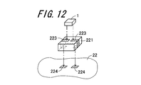
- the protruding portion 221 is shown as a submount substrate 221. As shown in FIG. 12, the submount substrate 221 is provided on the sub-base 22.
- FIG. 12 the submount substrate 221 is provided on the sub-base 22.
- the light emitting element 1 and the submount substrate 221 are shown in a state of being disassembled from the sub-base 22.
- the submount substrate 221 is shown in a transparent state for the purpose of showing the structure of the lower surface.
- the see-through structure is indicated by a dotted line.
- the submount substrate 221 has a plurality of conductor patterns 223.
- the plurality of conductor patterns 223 are electrically connected to the plurality of conductor patterns 224 of the sub-base 22 by a conductive bonding material.
- the exemplary submount substrate 221 is substantially made of silicon.
- Another exemplary submount substrate consists essentially of ceramics.
- the light emitting element 1 is electrically connected to the plurality of conductor patterns 223 of the submount substrate 221 with a conductive bonding material.
- the light emitting element 1 is mounted on the upper surface of the submount substrate 221.
- the light emitting device in this embodiment is improved in terms of thermal control by including the submount substrate 221. More specifically, the light emitting device is improved with respect to thermal control by including the submount substrate 221 having a higher thermal conductivity than the annular member 213. Therefore, the light emitting device in this embodiment is improved with respect to the light emission characteristics. Since the light emitting device according to the present embodiment includes the submount substrate 221, the portion including the mounting region of the light emitting element 1 and the annular member 213 can be formed of different materials.
- the submount substrate 221 is substantially made of silicon, and the annular member 213 is substantially made of ceramics.
- the portion including the mounting region of the light emitting element 1 and the annular member 213 can be made of different materials, and therefore, thermal control is improved.
- FIG. 13 another embodiment of the present invention will be described.
- the light emitting device in another embodiment includes the light emitting element 1, the base 2, and the light transmissive layer 3, similarly to the light emitting device shown in FIGS. 4 and 5.
- the light emitting device further includes a lens 4 and a wavelength conversion member 5.
- the light emitting device according to another embodiment is different from the light emitting device shown in FIGS.
- the first portion 211 is formed as a part of the sub-base 22.
- the first portion 211 is formed as a part of the sub-base 22, so that the overall strength is improved. Therefore, the light emitting device of this embodiment is improved with respect to light emission characteristics such as light emission distribution.
- the first part 211 is formed as a part of the sub-base 22, so that the number of parts is reduced.
- the light emitting device in another embodiment includes the light emitting element 1, the base 2, and the light transmissive layer 3, similarly to the light emitting device shown in FIGS.
- the light emitting device further includes a lens 4 and a wavelength conversion member 5.
- the light emitting device according to another embodiment is different from the light emitting device shown in FIGS. 4 and 5 in the structure relating to the first portion 211 and the second portion 212 of the base 2.
- the first portion 211 and the second portion 212 are formed as a part of the sub-base 22.
- the first portion 211 and the second portion 212 are integrally formed.
- the first portion 211 and the second portion 212 are formed as a part of the sub-base 22, so that the overall strength is improved. Therefore, the light emitting device of this embodiment is improved with respect to light emission characteristics such as light emission distribution.
- the first part 211 and the second part 212 are formed as a part of the sub-base 22, so that the number of parts is reduced.
- the light emitting device in another embodiment includes the light emitting element 1, the base 2, and the light transmissive layer 3, similarly to the light emitting device shown in FIGS. 4 and 5.
- the light emitting device further includes a lens 4 and a wavelength conversion member 5.
- the light emitting device according to another embodiment is different from the light emitting device shown in FIGS. 4 and 5 in the structure relating to the translucent layer 3.
- the translucent layer 3 is in partial contact with the inner surface of the annular member 213.
- the translucent layer 3 partially enters between the annular member 213 and the protruding portion 221.
- the light emitting device of this embodiment is improved with respect to the shape of the translucent layer 3 because the translucent layer 3 is partially in contact with the inner surface of the annular member 213. More specifically, in the manufacturing process, the light-transmitting layer 3 in the softened state is controlled with respect to the formation region or shape by the annular member 213.
- the light emitting device of the present embodiment is improved with respect to the light emission characteristics such as the light emission distribution by improving the shape of the translucent layer 3.
- the light emitting device in another embodiment includes the light emitting element 1, the base 2, and the translucent layer 3, similarly to the light emitting device shown in FIG. 15.
- the light emitting device further includes a lens 4 and a wavelength conversion member 5.
- the light emitting device according to another embodiment is different from the light emitting device shown in FIG. 15 in the structure related to the protruding portion 221 of the base 2.
- the protruding portion 221 is a submount substrate.
- the protruding portion 221 is shown as a submount substrate 221.
- the light emitting device in this embodiment is improved in terms of thermal control by including the submount substrate 221. More specifically, the light emitting device is improved with respect to thermal control by including the submount substrate 221 having a higher thermal conductivity than the annular member 213. Therefore, the light emitting device in this embodiment is improved with respect to the light emission characteristics.
- the light emitting device in another embodiment includes the light emitting element 1, the base 2, and the translucent layer 3, similarly to the light emitting device shown in FIG. 15.
- the light emitting device further includes a lens 4 and a wavelength conversion member 5.
- the light emitting device according to another embodiment is different from the light emitting device shown in FIG. 15 in the structure relating to the first portion 211 of the base 2.
- the first portion 211 is formed as a part of the sub-base 22.
- the first portion 211 is formed as a part of the sub-base 22, so that the overall strength is improved. Therefore, the light emitting device of this embodiment is improved with respect to light emission characteristics such as light emission distribution.
- the first part 211 is formed as a part of the sub-base 22, so that the number of parts is reduced.
- the light emitting device in another embodiment includes the light emitting element 1, the base 2, and the translucent layer 3, similarly to the light emitting device shown in FIG. 15.
- the light emitting device further includes a lens 4 and a wavelength conversion member 5.
- the light emitting device according to another embodiment is different from the light emitting device shown in FIG. 15 in the structure relating to the first portion 211 and the second portion 212 of the base 2.
- the first portion 211 and the second portion 212 are formed as a part of the sub-base 22.
- the first portion 211 and the second portion 212 are integrally formed.
- the first portion 211 and the second portion 212 are formed as a part of the sub-base 22, so that the overall strength is improved. Therefore, the light emitting device of this embodiment is improved with respect to light emission characteristics such as light emission distribution.
- the first part 211 and the second part 212 are formed as a part of the sub-base 22, so that the number of parts is reduced.
- the present invention can be implemented in various other forms without departing from the spirit or main features thereof. Therefore, the above-described embodiment is merely an example in all respects, and the scope of the present invention is shown in the claims, and is not restricted by the text of the specification. Further, all modifications and changes belonging to the scope of the claims are within the scope of the present invention.
Landscapes
- Led Device Packages (AREA)
Abstract
Description
本発明の一つの態様によれば、発光装置は、発光素子、基体および透光性層を含んでいる。基体は、第1部分および第2部分を含む上側部分を有している。第1部分は、発光素子の実装領域を含んでいるとともに第1気孔率を有している。第2部分は、第1部分を囲んでおり、複数の透光性粒子を含んでいるとともに、第1気孔率より大きい第2気孔率を有している。透光性層は、発光素子を封入しているとともに、第2部分から離間された状態で第1部分に付着している。
発光素子1は、基体2に実装されている。例示的な発光素子1は、半導体材料を含んでいる発光ダイオードである。発光素子1は、駆動電力に応じて第1次光を放射する。
基体2は、第1部分211および第2部分212を含む上側部分21を有している。第1部分211は、第1気孔率を有している。第2部分212は、第1部分211を囲んでいる。第2部分212は、複数の透光性粒子を含んでおり、第1気孔率より大きい第2気孔率を有している。
図3を参照して、第2部分212の構造について説明する。複数の透光性粒子401は、部分的に一体化されている。複数のセル402が、複数の透光性粒子401の間に存在している。透光性粒子401は、セル402より大きい屈折率を有している。発光素子1から放射された第1次光10は、透光性粒子401に入射される。透光性粒子401およびセル402の界面403は、透光性粒子401に入射された第1次光10を全反射によって反射する。第1次光10が臨界角θ403以上の入射角θ401を有する場合に、界面403は第1次光10を全反射によって反射する。臨界角θ403は、次の式によって表される。
sinθ403=n402/n401
n401は、透光性粒子401の屈折率を表している。n402は、セル402の屈折率を表している。
再び図1および図2を参照して、透光性層3は、第2部分から離間された状態で第1部分に付着している。ここで“離間”とは、図2に示されているように、透光性層3および第2部分212の間に、距離32が存在することである。透光性層3は、発光素子1を封入している。
以下、図面を参照して本発明のいくつかの例示的な実施形態を説明する。
図4および図5に示されているように、本発明の一つの実施形態における発光装置は、発光素子1、基体2および透光性層3を含んでいる。発光装置は、レンズ4および波長変換部材5をさらに含んでいる。図4において、波長変換部材5の内側構造を示すために、波長変換部材5は、部分的に省略されている。図4において、発光装置は、仮想のxyz空間におけるxy平面に実装されている。図4において、上方向とは、仮想のz軸の正方向のことをいう。
発光素子1は、基体2に実装されている。例示的な発光素子1は、半導体材料を含んでいる発光ダイオードである。発光素子1は、駆動電力に応じて第1次光を放射する。第1次光は、395nmから410nmまでの範囲に含まれるピーク発光波長を有している。
基体2は、第1部分211および第2部分212を含む上側部分21を有している。基体2は、突出部221を有しているサブ基体22を含んでいる。発光素子1の実装領域は、突出部221の上面に設けられている。第1部分211は、環状部材213および突出部221を含んでいる。本実施形態の発光装置は、突出部221を含むサブ基体を有していることにより、全体的な強度に関して改善されている。したがって、発光装置は、たとえば発光分布などの発光特性に関して改善されている。
図6に示されているように、例示的な環状部材213は、リング形状を有している。図6において、基体2は、分解された状態で示されている。環状部材213は、サブ基体22の上に設けられており、サブ基体22の突出部221を囲んでいる。環状部材213は、実質的にセラミックスからなる。環状部材213は、0.001%から1%までの範囲に含まれる第1気孔率を有している。本実施形態における環状部材213の気孔率の例示的な測定方法は、マイクロメリティクス(Micromeritics)社製のポアサイザー(Pore Sizer)9310型による水銀圧入法である。
例示的な第2部分212は、リング形状を有している。第2部分212は、サブ基体22の上に設けられており、第1部分211を囲んでいる。第2部分212は、複数の透光性粒子を含んでいる。複数の透光性粒子は、部分的に一体化されている。複数のセルが、複数の透光性粒子の間に存在している。第2部分212は、ポーラス状に形成されている。第2部分212は、15%から43%までの範囲に含まれる第2気孔率を有している。本実施形態における第2部分212の気孔率の例示的な測定方法は、マイクロメリティクス(Micromeritics)社製のポアサイザー(Pore Sizer)9310型による水銀圧入法である。第2気孔率は、第1気孔率より大きい。例示的な第2部分212は、実質的にセラミックスからなる。
例示的なサブ基体22は、実質的にセラミックスからなる。サブ基体22は、0.001%から1%までの範囲に含まれる気孔率を有している。本実施形態におけるサブ基体22の気孔率の測定方法は、マイクロメリティクス(Micromeritics)社製のポアサイザー(Pore Sizer)9310型による水銀圧入法である。図7に示されているように、サブ基体22は、複数の電気的経路222を有している。発光素子1は、導電性接合材を介して、複数の電気的経路222に電気的に接続されている。例示的な発光装置において、発光素子1は、フリップチップ接続によって、サブ基体22の突出部221に実装されている。
再び図4および図5を参照して、透光性層3は、基体2の上に設けられている。透光性層3は、第2部分212から離間された状態で第1部分211に付着しており、発光素子1を封入している。層3の“透光性”とは、発光素子1から放射された第1次光の少なくとも一部が透過できることをいう。例示的な透光性層3は、実質的にシリコーン樹脂からなる。透光性層3は、第1部分211の上面に付着している。
レンズ4は、透光性層3の上に設けられている。レンズ4は透光性を有している。レンズ4の透光性とは、発光素子1から放射された第1次光の少なくとも一部が透過できることをいう。例示的なレンズ4は、実質的にガラス材料からなる。
波長変換部材5は、基体2の上に設けられている。波長変換部材5は、空隙を介して、発光素子1、透光性層3およびレンズ4を覆っている。波長変換部材5は、ドーム形状を有している。波長変換部材5は、発光素子1から放射された第1次光に応じて第2次光を放射する。波長変換部材5は、マトリクス部材および複数の蛍光粒子を含んでいる。マトリクス部材は、透光性材料を含んでいる。マトリクス部材の透光性とは、発光素子1から放射された第1次光の少なくとも一部が透過できることをいう。例示的なマトリクス材料は、シリコーン樹脂である。複数の蛍光粒子は、発光素子1から放射された第1次光によって励起される。複数の蛍光粒子は、第2次光を放射する。複数の蛍光材料から放射された第2次光は、マトリクス材料を透過する。
本実施形態の発光装置は、ポーラス状に形成された第2部分212を含んでいる。したがって、発光装置は、発光強度に関して改善されている。さらに具体的には、第2部分212がポーラス状に形成されていることにより、第2部分は光反射効率に関して改善されている。第2部分212は、全反射によって、第1次光および第2次光を反射する。
本実施形態における発光装置は、第1部分211および透光性層3を含んでいる。第1部分は、第2部分の第2気孔率より小さい第1気孔率を有している。透光性層3は、第2部分から離間された状態で、第1部分211に付着している。したがって、発光装置は、たとえば発光分布などの発光特性に関して改善されている。第1部分が、第2部分の第2気孔率より小さい第1気孔率を有していることにより、透光性層3は、形状に関して改善されている。透光性層3は、製造工程における変形に関して低減されている。
本実施形態において、波長変換部材5は、ポーラス状に形成された第2部分212に接着されている。したがって、発光装置は、発光強度に関して改善されている。具体的には、発光素子1から放射された第1次光が第2部分212によって反射されることにより、波長変換部材5に入射される第1次光が増大される。波長変換部材5から放射された第2次光が第2部分212によって反射されることにより、発光装置の発光量が増大される。
本実施形態における発光装置の例示的な製造方法は、図8に示された複数の工程を含んでいる。符号802によって示された工程は、サブ基体22の上に環状部材213を設けることである。環状部材213は、サブ基体22の突出部221を囲んでおり、接合部材によってサブ基体22に固定される。符号804によって示された工程は、サブ基体22に発光素子1を実装することである。符号806によって示された工程は、透光性層3によって発光素子1を封入することである。透光性層3の例示的材料は、シリコーン樹脂である。軟化状態のシリコーン樹脂は、発光素子1を封入している状態で、第1部分211の上に設けられる。第1部分211が多孔質でないことにより、軟化状態のシリコーン樹脂は、変形に関して低減されている。透光性層3が設けられた後に、レンズ4が、透光性層3の上に設けられる。図9Aおよび図9Bに示されているように、透光性層3は、全体的に、第1部分211の上面の縁より内側に設けられている。
再び図8を参照して、符号808によって示された工程は、サブ基体22の上に第2部分を設けることである。第2部分212は、第1部分211を囲んでおり、接合部材によってサブ基体22に固定される。図10Aおよび図10Bに示されているように、透光性層3は、全体的に、第2部分212の上面の内側の縁よりさらに内側に設けられている。
再び図8を参照して、符号810によって示された工程は、第2部分212の上に波長変換部材5を設けることである。波長変換部材5は、接合部材によって第2部分212に固定される。波長変換部材5は、第2部分212に接着される前に成形されているという意味において、予め製造されているものである。したがって、波長変換部材5は、多孔質状に形成された第2部分212に接着される工程において、形状の変形に関して改善されている。
図11を参照して、本発明の他の実施形態について説明する。他の実施形態における発光装置は、図4および図5に示された発光装置と同様に、発光素子1、基体2および透光性層3を含んでいる。発光装置は、レンズ4および波長変換部材5をさらに含んでいる。
他の実施形態における発光装置において、図4および図5に示された発光装置と異なる点は、基体2の突出部221に関する構造である。本実施形態において、突出部221は、サブマウント基板である。以下、本実施形態において、突出部221は、サブマウント基板221として示されている。
図12に示されているように、サブマウント基板221は、サブ基体22の上に設けられている。図12において、発光素子1およびサブマウント基板221は、サブ基体22から分解された状態で示されている。図12において、サブマウント基板221は、下面の構造を示すことを目的に、透視された状態で示されている。サブマウント基板221において、透視された構造が点線によって示されている。
サブマウント基板221は、複数の導体パターン223を有している。複数の導体パターン223は、導電性接合材によって、サブ基体22の複数の導体パターン224に電気的に接続されている。例示的なサブマウント基板221は、実質的にシリコンからなる。他の例示的なサブマウント基板は、実質的にセラミックスからなる。
発光素子1は、導電性接合材によって、サブマウント基板221の複数の導体パターン223に電気的に接続されている。発光素子1は、サブマウント基板221の上面に実装されている。
本実施形態における発光装置は、サブマウント基板221を含んでいることにより、熱制御に関して改善されている。さらに具体的に、発光装置は、環状部材213より熱伝導率の高いサブマウント基板221を含んでいることにより、熱制御に関して改善されている。したがって、本実施形態における発光装置は、発光特性に関して改善されている。
本実施形態における発光装置は、サブマウント基板221を含んでいることにより、発光素子1の実装領域を含む部分と環状部材213とを異なる材料によって構成させることができる。例示的な発光装置において、サブマウント基板221は実質的にシリコンからなり、環状部材213は実質的にセラミックスからなる。本実施形態の発光装置は、発光素子1の実装領域を含む部分と環状部材213とを異なる材料によって構成させることができるため、熱制御に関して改善されている。
図13を参照して、本発明の他の実施形態について説明する。他の実施形態における発光装置は、図4および図5に示された発光装置と同様に、発光素子1、基体2および透光性層3を含んでいる。発光装置は、レンズ4および波長変換部材5をさらに含んでいる。
他の実施形態における発光装置において、図4および図5に示された発光装置と異なる点は、基体2の第1部分211に関する構造である。本実施形態において、第1部分211は、サブ基体22の一部分として形成されている。
本実施形態の発光装置は、第1部分211がサブ基体22の一部分として形成されていることにより、全体的な強度に関して改善されている。したがって、本実施形態の発光装置は、たとえば発光分布などの発光特性に関して改善されている。本実施形態の発光装置は、第1部分211がサブ基体22の一部分として形成されていることにより、部品点数に関して低減されている。
図14を参照して、本発明の他の実施形態について説明する。他の実施形態における発光装置は、図4および図5に示された発光装置と同様に、発光素子1、基体2および透光性層3を含んでいる。発光装置は、レンズ4および波長変換部材5をさらに含んでいる。
他の実施形態における発光装置において、図4および図5に示された発光装置と異なる点は、基体2の第1部分211および第2部分212に関する構造である。本実施形態において、第1部分211および第2部分212は、サブ基体22の一部分として形成されている。第1部分211および第2部分212は、一体的に形成されている。
本実施形態の発光装置は、第1部分211および第2部分212がサブ基体22の一部分として形成されていることにより、全体的な強度に関して改善されている。したがって、本実施形態の発光装置は、たとえば発光分布などの発光特性に関して改善されている。本実施形態の発光装置は、第1部分211および第2部分212がサブ基体22の一部分として形成されていることにより、部品点数に関して低減されている。
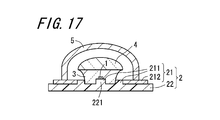
図15を参照して、本発明の他の実施形態について説明する。他の実施形態における発光装置は、図4および図5に示された発光装置と同様に、発光素子1、基体2および透光性層3を含んでいる。発光装置は、レンズ4および波長変換部材5をさらに含んでいる。
他の実施形態における発光装置において、図4および図5に示された発光装置と異なる点は、透光性層3に関する構造である。本実施形態において、透光性層3は、環状部材213の内側表面に部分的に接している。透光性層3は、環状部材213および突出部221の間に、部分的に入り込んでいる。
本実施形態の発光装置は、透光性層3が環状部材213の内側表面に部分的に接していることにより、透光性層3の形状に関して改善されている。さらに具体的に、製造工程において、軟化状態の透光性層3は、環状部材213によって、形成領域または形状に関して制御されている。本実施形態の発光装置は、透光性層3の形状に関して改善されていることにより、たとえば発光分布などの発光特性に関して改善されている。
図16を参照して、本発明の他の実施形態について説明する。他の実施形態における発光装置は、図15に示された発光装置と同様に、発光素子1、基体2および透光性層3を含んでいる。発光装置は、レンズ4および波長変換部材5をさらに含んでいる。
他の実施形態における発光装置において、図15に示された発光装置と異なる点は、基体2の突出部221に関する構造である。本実施形態において、突出部221は、サブマウント基板である。以下、本実施形態において、突出部221は、サブマウント基板221として示されている。
本実施形態における発光装置は、サブマウント基板221を含んでいることにより、熱制御に関して改善されている。さらに具体的に、発光装置は、環状部材213より熱伝導率の高いサブマウント基板221を含んでいることにより、熱制御に関して改善されている。したがって、本実施形態における発光装置は、発光特性に関して改善されている。
図17を参照して、本発明の他の実施形態について説明する。他の実施形態における発光装置は、図15に示された発光装置と同様に、発光素子1、基体2および透光性層3を含んでいる。発光装置は、レンズ4および波長変換部材5をさらに含んでいる。
他の実施形態における発光装置において、図15に示された発光装置と異なる点は、基体2の第1部分211に関する構造である。本実施形態において、第1部分211は、サブ基体22の一部分として形成されている。
本実施形態の発光装置は、第1部分211がサブ基体22の一部分として形成されていることにより、全体的な強度に関して改善されている。したがって、本実施形態の発光装置は、たとえば発光分布などの発光特性に関して改善されている。本実施形態の発光装置は、第1部分211がサブ基体22の一部分として形成されていることにより、部品点数に関して低減されている。
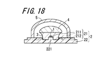
図18を参照して、本発明の他の実施形態について説明する。他の実施形態における発光装置は、図15に示された発光装置と同様に、発光素子1、基体2および透光性層3を含んでいる。発光装置は、レンズ4および波長変換部材5をさらに含んでいる。
他の実施形態における発光装置において、図15に示された発光装置と異なる点は、基体2の第1部分211および第2部分212に関する構造である。本実施形態において、第1部分211および第2部分212は、サブ基体22の一部分として形成されている。第1部分211および第2部分212は、一体的に形成されている。
本実施形態の発光装置は、第1部分211および第2部分212がサブ基体22の一部分として形成されていることにより、全体的な強度に関して改善されている。したがって、本実施形態の発光装置は、たとえば発光分布などの発光特性に関して改善されている。本実施形態の発光装置は、第1部分211および第2部分212がサブ基体22の一部分として形成されていることにより、部品点数に関して低減されている。
本発明は、その精神または主要な特徴から逸脱することなく、他のいろいろな形態で実施できる。したがって、前述の実施形態はあらゆる点で単なる例示に過ぎず、本発明の範囲は特許請求の範囲に示すものであって、明細書本文には何ら拘束されない。さらに、特許請求の範囲に属する変形や変更は全て本発明の範囲内のものである。
Claims (11)
- 発光素子と、
第1部分および第2部分を含む上側部分を有しており、前記第1部分が、前記発光素子の実装領域を含んでいるとともに第1気孔率を有しており、前記第2部分が、前記第1部分を囲んでおり、複数の透光性粒子を含んでいるとともに、前記第1気孔率より大きい第2気孔率を有している、基体と、
前記発光素子を封入しているとともに、前記第2部分から離間された状態で前記第1部分に付着している透光性層と、
を備えた発光装置。 - 前記基体が、前記実装領域を有する突出部を含むサブ基体を有していることを特徴とする請求項1記載の発光装置。
- 前記基体が、前記実装領域を有するサブマウント基板を有していることを特徴とする請求項1記載の発光装置。
- 前記サブマウント基板が、シリコンを含んでいることを特徴とする請求項3記載の発光装置。
- 前記サブマウント基板が、セラミックスを含んでいることを特徴とする請求項3記載の発光装置。
- 前記基体が、前記第1部分を含むサブ基体を有していることを特徴とする請求項1記載の発光装置。
- 前記第1部分および前記第2部分が一体的に形成されていることを特徴とする請求項1記載の発光装置。
- 前記第1部分が、前記実装領域から離間された環状部材を有していることを特徴とする請求項1記載の発光装置。
- 前記透光性層が、前記実装領域および前記環状部材の間に入り込んでいることを特徴とする請求項8記載の発光装置。
- 前記透光性層を覆っており、前記第2部分に接着された波長変換部材をさらに備えていることを特徴とする請求項1記載の発光装置。
- 前記第2部分がセラミックスを含んでいることを特徴とする請求項1記載の発光装置。
Priority Applications (4)
| Application Number | Priority Date | Filing Date | Title |
|---|---|---|---|
| EP08863914.1A EP2237330B1 (en) | 2007-12-25 | 2008-12-25 | Light emitting device |
| US12/810,487 US8384119B2 (en) | 2007-12-25 | 2008-12-25 | Light emitting device |
| CN2008801225984A CN101911316B (zh) | 2007-12-25 | 2008-12-25 | 发光装置 |
| JP2009547133A JP5111522B2 (ja) | 2007-12-25 | 2008-12-25 | 発光装置 |
Applications Claiming Priority (6)
| Application Number | Priority Date | Filing Date | Title |
|---|---|---|---|
| JP2007-332914 | 2007-12-25 | ||
| JP2007-332913 | 2007-12-25 | ||
| JP2007332914 | 2007-12-25 | ||
| JP2007332913 | 2007-12-25 | ||
| JP2007333716 | 2007-12-26 | ||
| JP2007-333716 | 2007-12-26 |
Publications (1)
| Publication Number | Publication Date |
|---|---|
| WO2009081980A1 true WO2009081980A1 (ja) | 2009-07-02 |
Family
ID=40801278
Family Applications (1)
| Application Number | Title | Priority Date | Filing Date |
|---|---|---|---|
| PCT/JP2008/073591 Ceased WO2009081980A1 (ja) | 2007-12-25 | 2008-12-25 | 発光装置 |
Country Status (6)
| Country | Link |
|---|---|
| US (1) | US8384119B2 (ja) |
| EP (1) | EP2237330B1 (ja) |
| JP (1) | JP5111522B2 (ja) |
| CN (1) | CN101911316B (ja) |
| TW (1) | TWI389350B (ja) |
| WO (1) | WO2009081980A1 (ja) |
Cited By (1)
| Publication number | Priority date | Publication date | Assignee | Title |
|---|---|---|---|---|
| US20220247173A1 (en) * | 2019-09-02 | 2022-08-04 | Mitsubishi Electric Corporation | Dc power distribution system |
Families Citing this family (2)
| Publication number | Priority date | Publication date | Assignee | Title |
|---|---|---|---|---|
| TWI414714B (zh) | 2011-04-15 | 2013-11-11 | Lextar Electronics Corp | 發光二極體杯燈 |
| CN102588762A (zh) * | 2011-01-06 | 2012-07-18 | 隆达电子股份有限公司 | 发光二极管杯灯 |
Citations (4)
| Publication number | Priority date | Publication date | Assignee | Title |
|---|---|---|---|---|
| JP2005123457A (ja) * | 2003-10-17 | 2005-05-12 | Nichia Chem Ind Ltd | 発光デバイス及び発光デバイスの製造方法 |
| JP2006287132A (ja) * | 2005-04-04 | 2006-10-19 | Kyoritsu Elex Co Ltd | 発光ダイオード用パッケージ及び発光ダイオード |
| JP2007080870A (ja) * | 2005-09-09 | 2007-03-29 | Matsushita Electric Works Ltd | 発光装置 |
| JP2007214592A (ja) * | 2007-04-26 | 2007-08-23 | Kyocera Corp | 発光装置 |
Family Cites Families (10)
| Publication number | Priority date | Publication date | Assignee | Title |
|---|---|---|---|---|
| US6107213A (en) * | 1996-02-01 | 2000-08-22 | Sony Corporation | Method for making thin film semiconductor |
| EP1496551B1 (en) * | 2003-07-09 | 2013-08-21 | Nichia Corporation | Light emitting diode, method of manufacturing the same and lighting equipment incorporating the same |
| US8449973B2 (en) * | 2005-03-29 | 2013-05-28 | Kyocera Corporation | Reflective member, light-emitting device using same and illuminating device |
| JP4991173B2 (ja) * | 2005-04-27 | 2012-08-01 | 京セラ株式会社 | 発光素子搭載用基体ならびにこれを用いた発光装置 |
| JP4773755B2 (ja) * | 2005-07-01 | 2011-09-14 | ローム株式会社 | チップ型半導体発光素子 |
| DE102006032415A1 (de) * | 2005-09-30 | 2007-04-05 | Osram Opto Semiconductors Gmbh | Verfahren zur Herstellung eines strahlungsemittierenden Bauelements und strahlungsemittierendes Bauelement |
| JP4926481B2 (ja) * | 2006-01-26 | 2012-05-09 | 共立エレックス株式会社 | 発光ダイオード用パッケージ及び発光ダイオード |
| JP4744335B2 (ja) * | 2006-01-30 | 2011-08-10 | 京セラ株式会社 | 発光装置および照明装置 |
| CN1832216A (zh) * | 2006-02-23 | 2006-09-13 | 苏州共立电子工业有限公司 | 发光二极管用壳体及其发光二极管 |
| TWI338380B (en) * | 2006-10-11 | 2011-03-01 | Chuan Yu Hung | Light emitting diode incorporating high refractive index material |
-
2008
- 2008-12-25 JP JP2009547133A patent/JP5111522B2/ja not_active Expired - Fee Related
- 2008-12-25 EP EP08863914.1A patent/EP2237330B1/en not_active Not-in-force
- 2008-12-25 WO PCT/JP2008/073591 patent/WO2009081980A1/ja not_active Ceased
- 2008-12-25 CN CN2008801225984A patent/CN101911316B/zh not_active Expired - Fee Related
- 2008-12-25 US US12/810,487 patent/US8384119B2/en not_active Expired - Fee Related
- 2008-12-25 TW TW097150814A patent/TWI389350B/zh not_active IP Right Cessation
Patent Citations (4)
| Publication number | Priority date | Publication date | Assignee | Title |
|---|---|---|---|---|
| JP2005123457A (ja) * | 2003-10-17 | 2005-05-12 | Nichia Chem Ind Ltd | 発光デバイス及び発光デバイスの製造方法 |
| JP2006287132A (ja) * | 2005-04-04 | 2006-10-19 | Kyoritsu Elex Co Ltd | 発光ダイオード用パッケージ及び発光ダイオード |
| JP2007080870A (ja) * | 2005-09-09 | 2007-03-29 | Matsushita Electric Works Ltd | 発光装置 |
| JP2007214592A (ja) * | 2007-04-26 | 2007-08-23 | Kyocera Corp | 発光装置 |
Cited By (2)
| Publication number | Priority date | Publication date | Assignee | Title |
|---|---|---|---|---|
| US20220247173A1 (en) * | 2019-09-02 | 2022-08-04 | Mitsubishi Electric Corporation | Dc power distribution system |
| US11824353B2 (en) * | 2019-09-02 | 2023-11-21 | Mitsubishi Electric Corporation | DC power distribution system |
Also Published As
| Publication number | Publication date |
|---|---|
| TWI389350B (zh) | 2013-03-11 |
| JPWO2009081980A1 (ja) | 2011-05-06 |
| CN101911316A (zh) | 2010-12-08 |
| US20110084295A1 (en) | 2011-04-14 |
| TW200947758A (en) | 2009-11-16 |
| EP2237330A1 (en) | 2010-10-06 |
| EP2237330A4 (en) | 2013-03-20 |
| US8384119B2 (en) | 2013-02-26 |
| CN101911316B (zh) | 2012-06-27 |
| JP5111522B2 (ja) | 2013-01-09 |
| EP2237330B1 (en) | 2015-02-25 |
Similar Documents
| Publication | Publication Date | Title |
|---|---|---|
| JP4182783B2 (ja) | Ledパッケージ | |
| US7741772B2 (en) | White LED package structure having a silicon substrate and method of making the same | |
| JPWO2007111355A1 (ja) | 発光装置 | |
| US8502250B2 (en) | Light emitting diode package and light emitting diode module | |
| JP2015079917A (ja) | 半導体発光装置 | |
| KR101012936B1 (ko) | 광투과성 기판을 사용하여 봉지된 발광다이오드 패키지 및 그의 제조방법 | |
| JP5111522B2 (ja) | 発光装置 | |
| JP2009182085A (ja) | 発光装置 | |
| US20080048199A1 (en) | Light emitting device and method of making the device | |
| JP4976895B2 (ja) | 発光装置 | |
| JP2007080870A (ja) | 発光装置 | |
| JP2008072043A (ja) | 光半導体装置 | |
| TW201705539A (zh) | 發光封裝體及其製造方法 | |
| JP5451091B2 (ja) | 発光装置および照明装置 | |
| KR101982522B1 (ko) | 조명유닛 및 그 제조방법 | |
| US7994528B2 (en) | Light emitting device and method for manufacturing the same | |
| JP4861474B2 (ja) | 発光装置 | |
| JP2009158637A (ja) | 発光装置 | |
| JP2010129711A (ja) | 発光装置 | |
| JP2009158634A (ja) | 発光装置 | |
| WO2012037720A1 (zh) | 用于制造封装发光二极管的方法 | |
| JP2010129712A (ja) | 発光装置 | |
| CN205542882U (zh) | 发光二极管封装体 | |
| US20090321762A1 (en) | Light emitting diode | |
| JP2010129710A (ja) | 発光装置 |
Legal Events
| Date | Code | Title | Description |
|---|---|---|---|
| WWE | Wipo information: entry into national phase |
Ref document number: 200880122598.4 Country of ref document: CN |
|
| 121 | Ep: the epo has been informed by wipo that ep was designated in this application |
Ref document number: 08863914 Country of ref document: EP Kind code of ref document: A1 |
|
| WWE | Wipo information: entry into national phase |
Ref document number: 2009547133 Country of ref document: JP |
|
| NENP | Non-entry into the national phase |
Ref country code: DE |
|
| WWE | Wipo information: entry into national phase |
Ref document number: 2008863914 Country of ref document: EP |
|
| WWE | Wipo information: entry into national phase |
Ref document number: 12810487 Country of ref document: US |