WO2009084137A1 - Dispositif à semi-conducteur et son procédé de fabrication - Google Patents
Dispositif à semi-conducteur et son procédé de fabrication Download PDFInfo
- Publication number
- WO2009084137A1 WO2009084137A1 PCT/JP2008/002659 JP2008002659W WO2009084137A1 WO 2009084137 A1 WO2009084137 A1 WO 2009084137A1 JP 2008002659 W JP2008002659 W JP 2008002659W WO 2009084137 A1 WO2009084137 A1 WO 2009084137A1
- Authority
- WO
- WIPO (PCT)
- Prior art keywords
- semiconductor device
- base layer
- manufacturing
- semiconductor
- region
- Prior art date
- Legal status (The legal status is an assumption and is not a legal conclusion. Google has not performed a legal analysis and makes no representation as to the accuracy of the status listed.)
- Ceased
Links
Images










Classifications
-
- H—ELECTRICITY
- H10—SEMICONDUCTOR DEVICES; ELECTRIC SOLID-STATE DEVICES NOT OTHERWISE PROVIDED FOR
- H10D—INORGANIC ELECTRIC SEMICONDUCTOR DEVICES
- H10D86/00—Integrated devices formed in or on insulating or conducting substrates, e.g. formed in silicon-on-insulator [SOI] substrates or on stainless steel or glass substrates
- H10D86/01—Manufacture or treatment
- H10D86/021—Manufacture or treatment of multiple TFTs
- H10D86/0214—Manufacture or treatment of multiple TFTs using temporary substrates
-
- H—ELECTRICITY
- H10—SEMICONDUCTOR DEVICES; ELECTRIC SOLID-STATE DEVICES NOT OTHERWISE PROVIDED FOR
- H10D—INORGANIC ELECTRIC SEMICONDUCTOR DEVICES
- H10D86/00—Integrated devices formed in or on insulating or conducting substrates, e.g. formed in silicon-on-insulator [SOI] substrates or on stainless steel or glass substrates
- H10D86/40—Integrated devices formed in or on insulating or conducting substrates, e.g. formed in silicon-on-insulator [SOI] substrates or on stainless steel or glass substrates characterised by multiple TFTs
-
- H—ELECTRICITY
- H10—SEMICONDUCTOR DEVICES; ELECTRIC SOLID-STATE DEVICES NOT OTHERWISE PROVIDED FOR
- H10D—INORGANIC ELECTRIC SEMICONDUCTOR DEVICES
- H10D86/00—Integrated devices formed in or on insulating or conducting substrates, e.g. formed in silicon-on-insulator [SOI] substrates or on stainless steel or glass substrates
- H10D86/40—Integrated devices formed in or on insulating or conducting substrates, e.g. formed in silicon-on-insulator [SOI] substrates or on stainless steel or glass substrates characterised by multiple TFTs
- H10D86/60—Integrated devices formed in or on insulating or conducting substrates, e.g. formed in silicon-on-insulator [SOI] substrates or on stainless steel or glass substrates characterised by multiple TFTs wherein the TFTs are in active matrices
-
- H—ELECTRICITY
- H10—SEMICONDUCTOR DEVICES; ELECTRIC SOLID-STATE DEVICES NOT OTHERWISE PROVIDED FOR
- H10D—INORGANIC ELECTRIC SEMICONDUCTOR DEVICES
- H10D30/00—Field-effect transistors [FET]
- H10D30/01—Manufacture or treatment
- H10D30/021—Manufacture or treatment of FETs having insulated gates [IGFET]
- H10D30/0223—Manufacture or treatment of FETs having insulated gates [IGFET] having source and drain regions or source and drain extensions self-aligned to sides of the gate
- H10D30/0227—Manufacture or treatment of FETs having insulated gates [IGFET] having source and drain regions or source and drain extensions self-aligned to sides of the gate having both lightly-doped source and drain extensions and source and drain regions self-aligned to the sides of the gate, e.g. lightly-doped drain [LDD] MOSFET or double-diffused drain [DDD] MOSFET
-
- H—ELECTRICITY
- H10—SEMICONDUCTOR DEVICES; ELECTRIC SOLID-STATE DEVICES NOT OTHERWISE PROVIDED FOR
- H10D—INORGANIC ELECTRIC SEMICONDUCTOR DEVICES
- H10D30/00—Field-effect transistors [FET]
- H10D30/01—Manufacture or treatment
- H10D30/021—Manufacture or treatment of FETs having insulated gates [IGFET]
- H10D30/031—Manufacture or treatment of FETs having insulated gates [IGFET] of thin-film transistors [TFT]
- H10D30/0321—Manufacture or treatment of FETs having insulated gates [IGFET] of thin-film transistors [TFT] comprising silicon, e.g. amorphous silicon or polysilicon
- H10D30/0323—Manufacture or treatment of FETs having insulated gates [IGFET] of thin-film transistors [TFT] comprising silicon, e.g. amorphous silicon or polysilicon comprising monocrystalline silicon
-
- H—ELECTRICITY
- H10—SEMICONDUCTOR DEVICES; ELECTRIC SOLID-STATE DEVICES NOT OTHERWISE PROVIDED FOR
- H10D—INORGANIC ELECTRIC SEMICONDUCTOR DEVICES
- H10D30/00—Field-effect transistors [FET]
- H10D30/60—Insulated-gate field-effect transistors [IGFET]
- H10D30/601—Insulated-gate field-effect transistors [IGFET] having lightly-doped drain or source extensions, e.g. LDD IGFETs or DDD IGFETs
-
- H—ELECTRICITY
- H10—SEMICONDUCTOR DEVICES; ELECTRIC SOLID-STATE DEVICES NOT OTHERWISE PROVIDED FOR
- H10P—GENERIC PROCESSES OR APPARATUS FOR THE MANUFACTURE OR TREATMENT OF DEVICES COVERED BY CLASS H10
- H10P90/00—Preparation of wafers not covered by a single main group of this subclass, e.g. wafer reinforcement
- H10P90/19—Preparing inhomogeneous wafers
- H10P90/1904—Preparing vertically inhomogeneous wafers
- H10P90/1906—Preparing SOI wafers
- H10P90/1914—Preparing SOI wafers using bonding
- H10P90/1916—Preparing SOI wafers using bonding with separation or delamination along an ion implanted layer, e.g. Smart-cut
-
- H—ELECTRICITY
- H10—SEMICONDUCTOR DEVICES; ELECTRIC SOLID-STATE DEVICES NOT OTHERWISE PROVIDED FOR
- H10W—GENERIC PACKAGES, INTERCONNECTIONS, CONNECTORS OR OTHER CONSTRUCTIONAL DETAILS OF DEVICES COVERED BY CLASS H10
- H10W10/00—Isolation regions in semiconductor bodies between components of integrated devices
- H10W10/10—Isolation regions comprising dielectric materials
- H10W10/181—Semiconductor-on-insulator [SOI] isolation regions, e.g. buried oxide regions of SOI wafers
Definitions
- the present invention relates to a semiconductor device applied to, for example, a liquid crystal display device and a manufacturing method thereof.
- Such a liquid crystal display device has a configuration in which a liquid crystal layer is sandwiched between a pair of substrates, and one substrate is a semiconductor in which a plurality of TFTs (Thin-Film Transistors) are formed on a glass substrate. Configure the device.
- TFTs Thin-Film Transistors
- SOI Silicon on Insulator
- SiO 2 silicon oxide film
- the SOI substrate it is desirable to reduce the thickness of the single crystal silicon layer from the viewpoint of increasing the operation speed of the device and further reducing the parasitic capacitance.
- various methods such as mechanical polishing, chemical mechanical polishing (CMP), and a method using porous silicon are known.
- CMP chemical mechanical polishing
- a method by hydrogen implantation hydrogen is implanted into a semiconductor substrate, which is bonded to another substrate and then subjected to heat treatment to separate the semiconductor substrate along the hydrogen implantation layer.
- a smart cut method for transferring onto a substrate has been proposed by Bruel (see Non-Patent Document 1, Non-Patent Document 2, etc.).
- an SOI substrate which is a silicon substrate in which a single crystal silicon layer is formed on the surface of an insulating layer can be formed.
- a device such as a transistor over such a substrate structure, parasitic capacitance can be reduced and insulation resistance can be increased, so that high performance and high integration of the device can be achieved.
- the present inventors have formed a hydrogen injection layer on a semiconductor substrate on which at least a part of a semiconductor element such as a MOS transistor is formed, and separated the part of the semiconductor substrate to place the semiconductor element on another substrate. It has been found that the film can be manufactured in a thin film. Then, by using the other substrate as a transparent substrate, a semiconductor device in which a semiconductor layer is thinned can be applied to a liquid crystal display device.
- the threshold voltage of NMOS transistors and PMOS transistors formed by thinning on other substrates is greatly shifted by about 1 V or more in the negative voltage direction.
- Such a fluctuation in threshold voltage causes the balance of the threshold values and drain current values of the NMOS and PMOS transistors to be lost, so that a CMOS circuit constituted by these NMOS transistors and PMOS transistors is normal. There is a problem that it can not work.
- the threshold voltage to shift in the negative voltage direction.
- some of the P-type impurity elements such as boron introduced into the channel regions of the NMOS transistor and the PMOS transistor for threshold control are inactivated by combining with hydrogen implanted to separate the semiconductor substrate. Therefore, it can be considered that the function as the original P-type impurity element is lost.
- hydrogen is involved in oxygen atoms present in the silicon substrate and a thermal donor is formed, so that the channel region may be N-type (see Non-Patent Documents 3 and 4). As a result, the actual threshold voltage is expected to shift in the negative voltage direction from the target threshold voltage.
- the amount of implantation of P-type impurities such as boron into the channel formation region is increased in advance. It is conceivable that the P-type impurity concentration that finally functions electrically as an acceptor is appropriately adjusted.
- the effective P-type impurity ratio can be increased, but the strain point of the glass substrate (the temperature at which strain does not occur) is 600. Considering that the temperature is about 700 ° C., it is difficult to raise the heat treatment temperature.
- the present invention has been made in view of the above points, and the object of the present invention is to form an element formed on the base layer by thinning it on another substrate and to reduce the impurity concentration of the P-type region.
- the aim is to optimize with good accuracy and reproducibility.
- a method of manufacturing a semiconductor device includes a device part forming step of forming a device part including at least a part of an element in a base layer, and a release material for the base layer.
- This is followed by an ion implantation step in which a P-type impurity element is ion-implanted into the base layer in order to adjust the impurity concentration of the P-type region of the element.
- a heat treatment step which is performed after the separation step, heats the base layer to remove the peeling material from the base layer, and covers the side of the base layer separated and removed with respect to the heat-treated base layer.
- the method includes an insulating film forming step of forming an insulating film, and in the ion implantation step, the P-type impurity element is ion-implanted into the base layer through the insulating film.
- the P-type impurity element is preferably boron.
- the substrate may be a glass substrate or a single crystal silicon semiconductor substrate.
- the base layer is composed of a single crystal silicon semiconductor, a group IV semiconductor, a group II-VI compound semiconductor, a group III-V compound semiconductor, a group IV-IV compound semiconductor, a mixed crystal containing these group elements, and an oxide semiconductor.
- a group IV semiconductor a group II-VI compound semiconductor, a group III-V compound semiconductor, a group IV-IV compound semiconductor, a mixed crystal containing these group elements, and an oxide semiconductor.
- the peeling material is hydrogen or an inert element.
- the element may be at least one of a MOS transistor, a bipolar transistor, and a diode.
- the element may be a MOS transistor, and the P-type region may be a channel region of the MOS transistor.
- the element may be a bipolar transistor, and the P-type region may be a base region of the bipolar transistor.
- the element may be a PN junction diode, and the P-type region may be a P-type region of a PN junction diode.
- the semiconductor device is configured such that a base layer in which a part is separated and removed along a peeling layer containing hydrogen and a device portion including at least a part of the element is bonded to the substrate.
- the base layer includes a P-type impurity element, and a ratio of the electrically active P-type impurity element to the P-type impurity element included in the base layer is 80% or more and 100%.
- % Has a region that is less than or equal to%.
- the semiconductor device according to the present invention is configured such that a base layer in which a part is separated and removed along a peeling layer containing hydrogen and a device portion including at least a part of the element is bonded to the substrate.
- a semiconductor device comprising: an insulating layer formed continuously on both the surface of the base layer and the surface of the substrate in a region where the base layer is not provided, the base layer and the insulating layer comprising: The P-type impurity element is contained, and the concentration distribution of the P-type impurity element contained in the base layer and the insulating layer is continuous at the interface between the base layer and the insulating layer.
- the concentration of the P-type impurity element is preferably 5 ⁇ 10 16 cm ⁇ 3 or more and 1 ⁇ 10 18 cm ⁇ 3 .
- the carrier concentration of the electrically active P-type impurity element is preferably 5 ⁇ 10 16 cm ⁇ 3 or more and 1 ⁇ 10 18 cm ⁇ 3 .
- the P-type impurity element is preferably boron.
- the substrate may be a glass substrate or a single crystal silicon semiconductor substrate.
- the base layer is composed of a single crystal silicon semiconductor, a group IV semiconductor, a group II-VI compound semiconductor, a group III-V compound semiconductor, a group IV-IV compound semiconductor, a mixed crystal containing these group elements, and an oxide semiconductor.
- a group IV semiconductor a group II-VI compound semiconductor, a group III-V compound semiconductor, a group IV-IV compound semiconductor, a mixed crystal containing these group elements, and an oxide semiconductor.
- the element may be at least one of a MOS transistor, a bipolar transistor, and a diode.
- the element may be a MOS transistor, and the P-type region may be a channel region of the MOS transistor.
- the element may be a bipolar transistor, and the P-type region may be a base region of the bipolar transistor.
- the element may be a PN junction diode, and the P-type region may be a P-type region of a PN junction diode.
- part of hydrogen which is a peeling material introduced into a base layer such as a semiconductor layer forms a pair with a P-type impurity element such as boron and inactivates the impurity element.
- other hydrogen introduced into the base layer can be removed from the base layer by performing a heat treatment at a temperature of 600 ° C. or lower after forming the base layer on another substrate. Thereafter, all of the P-type impurity elements such as boron ion-implanted into the base layer can function electrically as P-type impurities without being affected by the N-type conversion by hydrogen.
- the threshold voltage of the transistor can be controlled with high accuracy and reproducibility. Furthermore, since it is not necessary to introduce a large amount of impurity elements into the channel region of the transistor, there is no problem of mobility reduction due to impurity scattering by the impurity elements.
- the method for manufacturing a semiconductor device according to the present invention is based on the above knowledge, and when manufacturing the semiconductor device, first, a device portion forming step is performed. In this step, a device portion including at least a part of the element is formed on the base layer.
- the base layer may be, for example, a single crystal silicon semiconductor, a group IV semiconductor, a group II-VI compound semiconductor, a group III-V compound semiconductor, a group IV-IV compound semiconductor, a mixed crystal containing these elements, and an oxide semiconductor. At least one selected from the group consisting of:
- a release layer forming step is performed, and a release material is ion-implanted into the base layer to form a release layer.
- a release material for example, hydrogen or an inert element can be applied.
- an affixing process is performed to affix the substrate layer on which the device portion is formed to the substrate.
- a glass substrate or a single crystal silicon semiconductor substrate can be used as the substrate.
- the substrate becomes transparent, so that the semiconductor device can be applied to a display device such as a liquid crystal display device.
- a separation step is performed to heat and remove the portion of the base layer in the depth direction along the release layer where the device portion of the base layer is not formed by heating the base layer attached to the substrate. To do. As a result, the substrate layer is thinned. As a result, it is possible to increase the operation speed of the device and reduce the parasitic capacitance. At this time, since the base layer is heated, simultaneously with the separation and removal of the release layer, the release substance contained in the base layer can be removed from the base layer.
- an ion implantation step is performed, and a P-type impurity element is ion-implanted into the base layer in order to adjust the impurity concentration in the P-type region of the element.
- the P-type impurity element it is possible to apply a P-type impurity element.
- the peeling material is removed from the base layer in the separation step, it is possible to suppress the inactivation of the P-type impurity element and maintain the function as the P-type impurity element.
- the amount of P-type impurity element implanted into the base layer can be reduced, a decrease in mobility due to impurity scattering is also suppressed.
- the semiconductor device manufactured in this way has a region where the proportion of the P-type impurity element that is electrically active in the P-type impurity element contained in the base layer is 80% or more and 100% or less. Is possible.
- a separate heat treatment step may be performed to heat the base layer and remove the peeling material from the base layer. By doing so, it becomes possible to reliably remove the peeling substance from the base layer.
- an insulating film forming step is performed to form an insulating film that covers the separated and removed side of the base layer, and then an ion implantation step is performed, and the base layer is interposed through the insulating film.
- a P-type impurity element may be ion-implanted. Therefore, in the semiconductor device manufactured as described above, the concentration distribution of the P-type impurity element contained in the base layer and the insulating layer is a continuous distribution at the interface between the base layer and the insulating layer.
- a heat treatment step may be performed after the separation step, and then a P-type impurity element may be ion-implanted into the base layer through the insulating film formed in the insulating film forming step.
- the P-type impurity element for adjusting the impurity concentration in the P-type region of the element is ion-implanted into the base layer after the base layer is heated, it is included in the base layer by heating. As a result, it is possible to suppress the inactivation of the P-type impurity element and maintain the function as the P-type impurity element. That is, the impurity concentration in the P-type region of the element can be optimized with high accuracy and reproducibility. Furthermore, since the injection amount of the P-type impurity element into the base layer can be reduced while maintaining the function of the P-type impurity element, a decrease in mobility due to impurity scattering can be suppressed.
- FIG. 1 is a cross-sectional view schematically showing a main structure of a semiconductor device.
- FIG. 2 is a cross-sectional view showing a thermal oxide film formed on a silicon substrate.
- FIG. 3 is a cross-sectional view showing a step of ion-implanting phosphorus.
- FIG. 4 is a cross-sectional view showing a state in which a thermal oxide film and an N well region are formed.
- FIG. 5 is a cross-sectional view showing the patterned thermal oxide film and silicon nitride film.
- FIG. 6 is a cross-sectional view showing a state in which a LOCOS oxide film is formed.
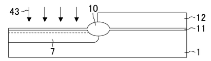
- FIG. 7 is a cross-sectional view showing a state where an oxide film is formed.
- FIG. 1 is a cross-sectional view schematically showing a main structure of a semiconductor device.
- FIG. 2 is a cross-sectional view showing a thermal oxide film formed on a silicon substrate.
- FIG. 3 is a cross
- FIG. 8 is a cross-sectional view showing a step of ion-implanting boron into the N well region.
- FIG. 9 is a cross-sectional view showing a step of ion-implanting boron.
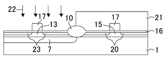
- FIG. 10 is a cross-sectional view showing a state in which a gate oxide film is formed.
- FIG. 11 is a cross-sectional view showing a state where the gate electrode is formed.
- FIG. 12 is a cross-sectional view showing a step of forming a low concentration impurity region.
- FIG. 13 is a cross-sectional view showing a step of forming a low concentration impurity region in the N well region.
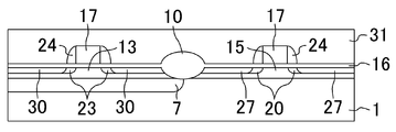
- FIG. 14 is a cross-sectional view showing a state in which a sidewall is formed.
- FIG. 15 is a cross-sectional view showing a step of forming a high concentration impurity region.
- FIG. 16 is a cross-sectional view showing a step of forming a high concentration impurity region in the N well region.
- FIG. 17 is a cross-sectional view showing a state in which a planarizing film is formed.
- FIG. 18 is a cross-sectional view showing a state where a release layer is formed.
- FIG. 19 is a cross-sectional view showing a state in which a source electrode and a drain electrode are formed.
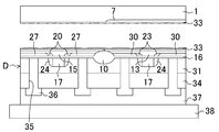
- FIG. 20 is a cross-sectional view showing the device portion attached to the glass substrate.
- FIG. 21 is an enlarged sectional view showing a state in which a part of the silicon substrate is separated.
- FIG. 22 is a cross-sectional view showing a state where ions are implanted through an oxide film.
- FIG. 23 is a cross-sectional view showing a device portion connected to an electric element on a glass substrate.
- FIG. 24 is a plan view showing the main part of the semiconductor device.
- S Semiconductor device D Device part 1 Silicon substrate (base layer) 4 N-type impurity element 10 LOCOS oxide film 13, 15 Channel region 16 Gate oxide film 17 Gate electrode 19 N-type impurity element 20 N-type low-concentration impurity region 22 P-type impurity element 23 P-type low-concentration impurity region 26 N-type impurity element 27 N-type high-concentration impurity region 29 P-type impurity element 30 P-type high-concentration impurity region 32 Release material 33 Release layer 38 Glass substrate (substrate) 39 Oxide film 40 Interlayer insulating film 43 Impurity element 45 Impurity element 50 P-type impurity element, boron 51 First active region 52 Second active region 56 PMOS transistor 57 NMOS transistor
- Embodiment 1 of the Invention 1 to 22 and 24 show Embodiment 1 of the present invention.
- FIG. 1 is a cross-sectional view schematically showing the main structure of the semiconductor device S.
- 2 to 22 are cross-sectional views showing each manufacturing process of the semiconductor device S.
- FIG. 24 is a plan view showing the main part of the semiconductor device S.
- the semiconductor device S is formed directly on the glass substrate 38 constituting the display panel of the liquid crystal display device.
- a driver circuit, a power supply circuit, and a clock that drive and control a plurality of pixels of the display panel. It is applied as various functional circuits such as a generation circuit, an input / output circuit, and a memory circuit.
- the liquid crystal display device is provided between a TFT substrate on which a plurality of TFTs (transistors) are formed, a counter substrate provided to face the TFT substrate, and the TFT substrate and the counter substrate.
- Liquid crystal layer For the counter substrate, a common electrode made of ITO or the like, a color filter, and the like are formed on a glass substrate.
- a plurality of TFTs, pixel electrodes and the like are formed on the glass substrate 38.
- the semiconductor device S includes a glass substrate 38 and a device portion D formed on the base layer 1 on the glass substrate 38 with high density and high accuracy.
- the device portion D includes transistors 56 and 57 that are elements, and the transistors 56 and 57 are covered with a planarizing film 37.
- the device portion D is bonded to the glass substrate 38 through the planarizing film 37 by self-bonding.
- the base layer 1 is attached to the glass substrate 38 together with the device portion D.
- the substrate 38 is preferably a transparent substrate such as a glass substrate 38, but when applied to other display devices or the like, the substrate 38 is Other substrates such as a single crystal silicon semiconductor substrate can be used.
- the device portion D includes an NMOS transistor 57 and a PMOS transistor 56, which are semiconductor elements, as shown in FIGS.
- a LOCOS oxide film 10 that is an element isolation film is formed.
- the PMOS transistor 56 on the right side in FIG. 1 schematically shows an AA cross section in FIG.
- the NMOS transistor 57 on the left side in FIG. 1 schematically shows a BB cross section in FIG.
- the devices to be formed are not limited to these, and can be applied to any semiconductor device. Also, the number is not limited from 1 to several million.
- the device portion D can be formed so as to include at least a part of the element.
- the base layer 1 has a first active region 51 formed in the right N well region 7 in FIG. 1 and a second active region 52 formed in the left region in FIG.
- the first active region 51 constitutes a PMOS transistor 56, while the second active region 52 constitutes an NMOS transistor 57.
- the first and second active regions 51 and 52 are formed on the left and right outer sides of the channel regions 13 and 15, respectively, and on the outer sides of the low concentration impurity regions 23 and 20, respectively.
- each has a LDD (Lightly Doped Drain) structure constituted by the high concentration impurity regions 30 and 27.
- the channel region 13 is formed in the first active region 51, and the P-type low-concentration impurity regions 23 disposed on the left and right sides thereof and the outside of the P-type low-concentration impurity region 23 are disposed. Further, a P-type high concentration impurity region 30 is formed.
- the channel region 15 is formed in the second active region 52, and the N-type low-concentration impurity regions 20 disposed on both the left and right sides of the channel region 15 and the N-type low-concentration impurity regions 20 are disposed respectively.
- N-type high concentration impurity region 27 is formed.
- the base layer 1 is a semiconductor layer such as a single crystal silicon semiconductor.
- the base layer 1 includes a group IV semiconductor, a group II-VI compound semiconductor, a group III-V compound semiconductor, a group IV-IV compound semiconductor, and a mixed crystal containing these homologous elements, In addition, at least one selected from the group consisting of oxide semiconductors can be included.
- a part of the base layer 1 is separated and removed along a release layer formed by ion implantation of a release material such as hydrogen as described later.
- a part of the substrate layer 1 is thinned by being separated and removed by heat treatment.
- a planarizing film 37 that is an insulating film is laminated on the surface of the glass substrate 38.
- An interlayer insulating film 34 and a planarizing film 31 are further stacked on the planarizing film 37.
- a gate oxide film 16 and a LOCOS oxide film 10 are formed on the planarizing film 31 .
- the base layer 1 in which the first active region 51 and the second active region 52 are formed is laminated.
- the surface of the base layer 1 is covered with an oxide film 39 as an insulating layer together with the LOCOS oxide film 10.
- the oxide film 39 is continuously formed on both the surface of the base layer 1 constituting the surface of the device portion D and the surface of the glass substrate 38 in a region where the base layer 1 is not provided. Further, the oxide film 39 is covered with an interlayer insulating film 40.
- a gate electrode 17 and sidewalls 24 made of, for example, polysilicon are formed between the planarization film 31 and the gate oxide film 16.
- the gate electrode 17 faces the channel regions 13 and 15 with the gate oxide film 16 in between.
- the sidewall 24 is disposed on the side of the gate electrode 17 and faces the low-concentration impurity regions 20 and 23 through the gate oxide film 16.
- contact holes 35 are formed penetratingly at positions overlapping with the high-concentration impurity regions 27 and 30.
- a source electrode 36 and a drain electrode 36 that are metal electrodes are formed in the contact hole 35, respectively.
- the semiconductor device S of the first embodiment has a CMOS structure. That is, as shown in FIG. 24, the metal wiring 36i to which the input voltage is applied is electrically connected to the gate electrode 17n of the NMOS transistor 57 and the gate electrode 17p of the PMOS transistor 56 through the contact hole 35g. . The drain regions of the NMOS transistor 57 and the PMOS transistor 56 are electrically connected to the metal wiring 36o from which the output voltage is extracted.
- the base layer 1 includes boron, which is a P-type impurity element, in the channel region 15 of the NMOS transistor 57 or the channel region 13 of the PMOS transistor 56.
- the base layer 1 is electrically out of the boron contained in the base layer 1. It has a region where the percentage of active boron is 80% or more and 100% or less.
- the concentration of boron in the base layer 1 is 5 ⁇ 10 16 cm ⁇ 3 or more and 1 ⁇ 10 18 cm ⁇ 3 .
- the carrier concentration of an electrically active P-type impurity element may be 5 ⁇ 10 16 cm ⁇ 3 or more and 1 ⁇ 10 18 cm ⁇ 3 .
- boron is contained not only in the base layer 1 but also in the oxide film 39, and the concentration distribution of boron contained in the base layer 1 and the oxide film 39 is continuous at the interface between the base layer 1 and the oxide film 39. ing.
- a device part D including at least a part of the NMOS transistor 57 and the PMOS transistor 56 which are elements is formed in the base layer 1 which is a single crystal silicon semiconductor layer. That is, as shown in FIG. 2, a thermal oxide film 2 having a thickness of about 30 nm is formed on a silicon substrate 1 (corresponding to the base layer 1) which is a wafer.
- the thermal oxide film 2 is intended to prevent contamination of the surface of the silicon substrate 1 in a step of performing ion implantation later, but is not necessarily essential.
- the silicon substrate 1 made of a single crystal silicon semiconductor has been described as an example of the base layer 1, the present invention is not limited to this, and can be formed of a material including other semiconductors.
- the base layer 1 includes a single crystal silicon semiconductor, a group IV semiconductor, a group II-VI compound semiconductor, a group III-V compound semiconductor, a group IV-IV compound semiconductor, a mixed crystal containing these group elements, and an oxide. It may be configured to include at least one selected from the group consisting of semiconductors.
- the N-type impurity element 4 (for example, phosphorus) is applied to the region to be the first active region 51.
- Ion implantation When phosphorus element is ion-implanted, the implantation energy is set to about 50 to 150 KeV and the dose is set to about 1 ⁇ 10 12 to 1 ⁇ 10 13 cm ⁇ 2 .
- P-type impurities such as boron are implanted into the N well region 7 over the entire surface of the silicon thin film.
- the amount of implantation of the N-type impurity element is additionally set in consideration of the amount canceled by the P-type impurity element.
- a thermal oxide film 6 having a thickness of about 30 nm is formed by performing a heat treatment at about 900 to 1000 ° in an oxidizing atmosphere, and an N well.
- the impurity element implanted into the region 7 is diffused to form an N well region 7.
- the silicon nitride film 9 and the thermal oxide film 6 are patterned as shown in FIG.
- an NMOS transistor 57 and a PMOS transistor 56 are formed later in the region where the silicon nitride film 9 and the thermal oxide film 6 are left.
- LOCOS oxidation is performed by performing heat treatment at about 900 to 1000 ° in an oxygen atmosphere.
- a LOCOS oxide film 10 having a thickness of about 200 to 500 nm and a thickness of, for example, 350 nm is formed.
- the LOCOS oxide film 10 is formed in a region exposed from the silicon nitride film 9 and the thermal oxide film 6.
- LOCOS oxidation is a method for element isolation, but element isolation may be performed by a method other than LOCOS oxidation, such as STI (Shallow Trench Isolation).
- heat treatment is performed at about 1000 ° C. in an oxygen atmosphere, and as shown in FIG. 7, heat of about 20 nm thickness is formed on the surface of the silicon substrate 1. An oxide film 11 is formed.
- a resist 12 is formed so that the formation region of the PMOS transistor 56 is opened.
- an impurity element 43 for setting the threshold voltage of the PMOS transistor 56 is introduced into the N well region 7 by ion implantation.
- the impurity element 43 to be implanted is an N-type impurity element such as phosphorus, the implantation is performed. If the impurity element 43 is a P-type impurity element such as boron, the implantation is not performed at this time. This step shown in FIG. 8 is omitted. Whether to implant N-type or P-type impurity elements is appropriately selected depending on the gate electrode material and its conductivity type.
- boron is generally implanted for setting the threshold voltage in consideration of the work function of the gate electrode, so this step is omitted.
- P + polysilicon is used for the gate electrode
- phosphorus is ion-implanted with a dose of about 1 ⁇ 10 12 to 1 ⁇ 10 13 cm ⁇ 2 and an energy of about 10 to 50 KeV. The dose is adjusted according to the threshold voltage that is the control target value.
- a resist 14 is formed so that the region of the NMOS transistor 57 is opened.
- an impurity element 45 for setting the threshold voltage of the NMOS transistor 57 is introduced into the silicon substrate 1 by ion implantation.
- the impurity element to be implanted is an N-type impurity such as phosphorus
- the implantation is performed.
- the impurity element 45 is a P-type impurity element such as boron, this time is used. No injection is performed, and this step shown in FIG. 9 is omitted.
- boron is generally implanted for setting the threshold voltage in consideration of the work function of the gate electrode, so this step is omitted.
- P + polysilicon is applied to the gate electrode
- phosphorus is ion-implanted with a dose of about 1 ⁇ 10 12 to 1 ⁇ 10 13 cm ⁇ 2 and an energy of about 10 to 50 KeV. The dose is adjusted according to the threshold voltage that is the control target value.
- the gate electrodes 17 of the NMOS transistor 57 and the PMOS transistor 56 are formed on the gate oxide film 16. That is, the gate electrode 17 is formed by depositing a polysilicon layer having a thickness of about 300 nm on the gate oxide film 16 by CVD or the like, and then introducing an N impurity element such as phosphorus into the gate electrode 17 by diffusion or the like. A polysilicon layer is used. Subsequently, the N + polysilicon layer is patterned by photolithography to form the gate electrode 17.
- a resist 18 is formed so as to open in a region where the NMOS transistor 57 is formed (the region on the right side in FIG. 12), and the N-type impurity element 19 is ionized using the gate electrode 17 as a mask. inject.
- an N-type low concentration impurity region 20 is formed in the silicon substrate 1.
- phosphorus is applied to the N-type impurity element 19.
- ion implantation is performed with an energy of about 10 to 50 KeV at a dose of about 1 ⁇ 10 13 to 1 ⁇ 10 14 cm ⁇ 2 .
- a resist 21 is formed so as to open in a region where the PMOS transistor 56 is formed (left region in FIG. 14), and the P-type impurity element 22 is ionized using the gate electrode 17 as a mask. inject. Thus, a P-type low concentration impurity region 23 is formed.
- the impurity element when a part of a P-type impurity element such as boron forms a pair with hydrogen, the impurity element is deactivated, so that the original function as a P-type impurity element is lost. Further, hydrogen is involved in oxygen atoms present in the silicon substrate 1, and as a result of the formation of a thermal donor, the P-type impurity element becomes N-type. Therefore, the dose amount of the P-type impurity is set in consideration of the proportion of the P-type impurity element that functions effectively.
- the P-type impurity is, for example, boron element
- the ion implantation condition is, for example, when boron (BF 2+ ) is implanted, with a dose amount of about 5 ⁇ 10 12 to 5 ⁇ 10 14 cm ⁇ 2 and 10 to 10 Ion implantation is performed with an energy of about 50 KeV.
- the P-type low-concentration impurity of the PMOS transistor 56 can be obtained only by thermal diffusion of boron implanted when forming the P-type high-concentration impurity region of the PMOS transistor 56 in a later process. A region may be formed. Therefore, ion implantation for forming the P-type low-concentration impurity region is not necessarily performed.
- the formation process of the P-type low concentration impurity region 23 is performed using the gate electrode 17 as a mask, it must be performed at this point after the formation of the gate electrode 17. Further, the P-type impurity element 22 introduced at this time does not directly affect the threshold voltage of the PMOS transistor, and therefore does not directly affect the accuracy and reproducibility of the threshold voltage.
- a SiO 2 film is formed by CVD or the like so as to cover the gate oxide film 16 and the LOCOS oxide film 10. Thereafter, anisotropic dry etching is performed on the SiO 2 film to form side walls 24 made of SiO 2 on both side walls of the gate electrode 17 as shown in FIG.
- a resist 25 is formed so as to open in the region where the NMOS transistor 57 is to be formed, and an N-type impurity element 26 such as phosphorus is applied to the silicon substrate using the gate electrode 17 and the sidewall 24 as a mask. 1 is ion-implanted.
- N-type high concentration impurity regions 27 are formed on both outer sides of the N-type low concentration impurity region 20.
- a resist 28 is formed so as to open in a region where the PMOS transistor 56 is formed, and a P-type impurity element 29 such as boron is applied to the silicon substrate using the gate electrode 17 and the sidewall 24 as a mask. 1 is ion-implanted.
- P-type high concentration impurity regions 30 are formed on both outer sides of the P-type low concentration impurity region 23.
- heat treatment is performed on the region where the impurity element is ion-implanted, and the impurity element is activated. For example, the heat treatment is performed at 900 ° C. for 10 minutes.
- planarizing film 31 having a thickness of about 600 nm.
- a release layer forming step is performed.
- the release material 33 is ion-implanted into the silicon substrate 1 through the planarizing film 31 to form the release layer 33.
- Hydrogen is applied to the peeling material 32.
- An inert element such as He or Ne can be applied instead of or in addition to hydrogen.
- ion implantation conditions for example, when the peeling material 32 is hydrogen, the dose is about 2 ⁇ 10 16 to 1 ⁇ 10 17 cm ⁇ 2 and the implantation energy is about 100 to 200 KeV.
- an interlayer insulating film 34 is formed on the surface of the planarizing film 31.
- a contact hole 35 is formed in the planarizing film 31 and the interlayer insulating film 34, and the high concentration impurity regions 27 and 30 are exposed at the bottom of the contact hole 35.
- the contact hole 35 is filled with a metal material to form a source electrode 36 and a drain electrode 36, which are metal electrodes, as shown in FIG.
- a contact hole 35 is similarly formed in the gate electrode 17, a metal material is filled therein, and a voltage is applied to the gate electrode 17.
- the metal electrode is formed. Note that the contact hole 35, the source electrode 36, and the drain electrode 36 are formed without forming the interlayer insulating film 34 by forming the planarizing film 31 formed before ion implantation of the peeling material 32 to be relatively thick. May be.
- a planarizing film 37 is formed so as to cover the NMOS transistor 57 and the PMOS transistor 56. That is, first, an insulating film is deposited on the interlayer insulating film 34 by CVD or the like. Next, the insulating film is polished by a CMP method or the like to flatten the surface.
- the device part forming step for forming the device part D including at least a part of the NMOS transistor 57 and the PMOS transistor 56 as the elements is performed on the base layer 1 as the silicon substrate 1.
- the pasting process is performed.
- the silicon substrate 1 (base layer 1) on which the device portion D is formed is attached to the substrate 38.
- a glass substrate 38 is applied to the substrate 38. That is, the surface of the planarizing film 37 and the surface of the glass substrate 38 are each cleaned by SC1.
- the SC1 cleaning liquid is made of ammonia, hydrogen peroxide, and water, and is used to make the surface of the object hydrophilic.
- the device part D is aligned with the glass substrate 38 and bonded to each other on the surface of the planarizing film 37 by self-bonding by van der Waals force.
- the silicon substrate 1 (base layer 1) affixed to the glass substrate 38 is heated to about 400 to 600 ° C., whereby the depth of the silicon substrate 1 (base layer 1) is increased.
- a part in the vertical direction that is, a part on the side opposite to the gate electrode 17 through the release layer 33 and the device part D is not formed) is separated and removed along the release layer 33.
- the NMOS transistor 57 and the PMOS transistor 56 are transferred onto the glass substrate 38.
- the substrate layer 1 (including the N well region 7) is thinned by etching or CMP until the LOCOS oxide film 10 is exposed, and element isolation is performed. Note that the step of etching the base layer 1 until the LOCOS oxide film 10 is exposed is not necessarily required.
- a heat treatment process is performed, and the base layer 1 is heated to remove hydrogen as a peeling material from the base layer 1. That is, hydrogen in the base layer 1 is removed by performing heat treatment at a temperature of 400 to 600 ° C. for about 30 minutes to 4 hours.
- an insulating film forming step is performed to form an oxide film 39 which is an insulating film covering the separated and removed side of the base layer 1 as shown in FIG.
- the oxide film 39 is formed to a thickness of about 10 to 100 nm by CVD or the like.
- the oxide film 39 is formed across the surface including the side surface of the device portion D and the surface of the glass substrate 38 on which the device portion D is not provided.
- boron 50 which is a P-type impurity element is ion-implanted through an oxide film 39. That is, the boron 50 is introduced from the side opposite to the gate electrode 17 in the base layer 1.
- the threshold voltages of the NMOS transistor 57 and the PMOS transistor 56 are adjusted.
- the dose is 1 ⁇ 10 12 to 1 ⁇ 10 13 cm ⁇ 2 and the implantation energy is about 20 to 100 KeV.
- the semiconductor device S manufactured in this way has a region where the proportion of electrically active boron in the boron contained in the base layer 1 is 80% or more and 100% or less. Further, the concentration distribution of boron contained in the base layer 1 and the oxide film 39 is a continuous distribution at the interface between the base layer 1 and the oxide film 39.
- an interlayer insulating film 40 is formed on the surface of the oxide film 39.
- a heat treatment at about 500 to 600 ° C. for about 30 minutes to 4 hours, or a short time (less than 10 minutes) at 600 to 700 ° C. so as not to adversely affect the glass substrate 38.
- the semiconductor device S is manufactured.
- the boron 50 for appropriately setting the threshold voltage by adjusting the impurity concentration of the P-type region in the NMOS transistor 57 and the PMOS transistor 56 Since ions are implanted into the base layer 1, hydrogen contained in the base layer 1 can be removed by heat treatment performed in advance in the separation step and the heat treatment step. As a result, inactivation of boron 50 introduced into the base layer 1 by hydrogen can be suppressed, and the function of the boron 50 as a P-type impurity element can be maintained. That is, the threshold voltages of the NMOS transistor 57 and the PMOS transistor 56 can be optimized with high accuracy and reproducibility. Furthermore, since the amount of boron 50 injected into the base layer 1 can be reduced while maintaining the function of the P-type impurity element, a decrease in mobility due to impurity scattering can also be suppressed.
- the operating speed of the NMOS transistor 57 and the PMOS transistor 56 can be increased and the parasitic capacitance can be reduced.
- the base layer 1 can be sufficiently heated to reliably remove hydrogen from the base layer 1.
- the heat treatment step for heat-treating the base layer 1 is performed separately from the separation step, but the heat treatment step for omitting the heat treatment step and removing hydrogen from the base layer 1 is performed. You may make it serve as the heat processing of the base layer 1 in a previous separation process. As a result, the number of steps can be shortened and the cost can be reduced.
- the example in which the device portion D is bonded to the glass substrate 38 has been described.
- FIG. 23 which is a cross-sectional view
- the glass substrate is compared with the electrical element 42 previously formed on the glass substrate 38.
- the NMOS transistor 57 and the PMOS transistor 56 of the device part D attached to 38 may be electrically connected.
- the device part D is pasted on the glass substrate 38 on which the electrical elements 42 such as active elements and passive elements are formed in advance. Thereafter, the heat treatment step is performed. Next, after forming the oxide film 39 so as to cover the device portion D and the electric element 42 on the glass substrate 38, the ion implantation process is performed. Next, an interlayer insulating film 40 is formed so as to cover the oxide film 39. Thereafter, a contact hole 46 is formed in the device portion D, and the source electrode 36 and the drain electrode 36 are exposed at the bottom of the contact hole 46. On the other hand, a contact hole 47 is formed in the oxide film 39 and the interlayer insulating film 40 on the side of the device portion D so that the electric element 42 is exposed. Then, the metal wiring 41 is patterned so as to connect the electric element 42 and the source electrode 36 or the drain electrode 36 through the contact holes 46 and 47. In this way, the semiconductor device S may be manufactured.
- the MOS transistor is described as an example of the element, but the present invention is not limited to this. That is, at least one of a MOS transistor, a bipolar transistor, and a diode can be similarly applied to the element.
- the P-type region can be applied as a channel region of the MOS transistor.
- the present invention can be applied to the P-type region as the base region of the bipolar transistor.
- the present invention can be similarly applied as a P-type region of the PN junction diode.
- the device portion D including at least a part of the NMOS transistor 57 and the PMOS transistor 56 as elements on the base layer 1 that is a single crystal silicon semiconductor layer, boron or the like
- the method of basically omitting the ion implantation step of the P-type impurity element has been described.
- Boron 50 which is a P-type impurity element, may be ion-implanted into the base layer 1 through the oxide film 39.
- a P-type impurity element is gated in a channel region of a MOS transistor having a fine element dimension in a plane in contact with a low concentration impurity region of a source region and a drain region in order to suppress a so-called short channel effect.
- ion implantation is performed from an oblique direction using an electrode as a mask (Halo implantation)
- the present invention is useful for a semiconductor device applied to, for example, a liquid crystal display device and a manufacturing method thereof, and in particular, an element formed on a base layer is formed by thinning on another substrate. At the same time, it is suitable for optimizing the impurity concentration of the P-type region with high accuracy and good reproducibility.
Landscapes
- Metal-Oxide And Bipolar Metal-Oxide Semiconductor Integrated Circuits (AREA)
- Element Separation (AREA)
- Thin Film Transistor (AREA)
Abstract
Priority Applications (2)
| Application Number | Priority Date | Filing Date | Title |
|---|---|---|---|
| US12/746,323 US20100295105A1 (en) | 2007-12-27 | 2008-09-25 | Semiconductor device and method for manufacturing the same |
| CN2008801223438A CN101911247B (zh) | 2007-12-27 | 2008-09-25 | 半导体装置及其制造方法 |
Applications Claiming Priority (2)
| Application Number | Priority Date | Filing Date | Title |
|---|---|---|---|
| JP2007-336332 | 2007-12-27 | ||
| JP2007336332 | 2007-12-27 |
Publications (1)
| Publication Number | Publication Date |
|---|---|
| WO2009084137A1 true WO2009084137A1 (fr) | 2009-07-09 |
Family
ID=40823875
Family Applications (1)
| Application Number | Title | Priority Date | Filing Date |
|---|---|---|---|
| PCT/JP2008/002659 Ceased WO2009084137A1 (fr) | 2007-12-27 | 2008-09-25 | Dispositif à semi-conducteur et son procédé de fabrication |
Country Status (3)
| Country | Link |
|---|---|
| US (1) | US20100295105A1 (fr) |
| CN (1) | CN101911247B (fr) |
| WO (1) | WO2009084137A1 (fr) |
Cited By (2)
| Publication number | Priority date | Publication date | Assignee | Title |
|---|---|---|---|---|
| JP2015216398A (ja) * | 2009-10-30 | 2015-12-03 | 株式会社半導体エネルギー研究所 | 半導体装置の作製方法 |
| JP2017135394A (ja) * | 2009-12-08 | 2017-08-03 | 株式会社半導体エネルギー研究所 | 半導体装置の作製方法 |
Families Citing this family (4)
| Publication number | Priority date | Publication date | Assignee | Title |
|---|---|---|---|---|
| US9997353B1 (en) * | 2010-12-24 | 2018-06-12 | Ananda H. Kumar | Silicon composite substrates |
| KR20130128227A (ko) * | 2012-05-16 | 2013-11-26 | 삼성전자주식회사 | 전자소자 탑재용 기판의 제조방법 |
| US10573627B2 (en) * | 2015-01-09 | 2020-02-25 | Silicon Genesis Corporation | Three dimensional integrated circuit |
| TWI716864B (zh) * | 2017-12-01 | 2021-01-21 | 美商矽基因股份有限公司 | 三維積體電路之形成方法 |
Citations (3)
| Publication number | Priority date | Publication date | Assignee | Title |
|---|---|---|---|---|
| JPH07161947A (ja) * | 1993-12-03 | 1995-06-23 | Fujitsu Ltd | Soi基板を用いた半導体装置及びその製造方法 |
| JP2006005245A (ja) * | 2004-06-18 | 2006-01-05 | Sharp Corp | 半導体基板の製造方法、及び半導体基板 |
| JP2007234628A (ja) * | 2006-02-27 | 2007-09-13 | Sharp Corp | 半導体装置及びその製造方法 |
Family Cites Families (4)
| Publication number | Priority date | Publication date | Assignee | Title |
|---|---|---|---|---|
| EP0204979B1 (fr) * | 1985-06-03 | 1989-03-29 | Siemens Aktiengesellschaft | Procédé de fabrication simultanée des transistors de type MOS complémentaires et bipolaires sur le même substrat en silicium |
| US6498376B1 (en) * | 1994-06-03 | 2002-12-24 | Seiko Instruments Inc | Semiconductor device and manufacturing method thereof |
| JP4319078B2 (ja) * | 2004-03-26 | 2009-08-26 | シャープ株式会社 | 半導体装置の製造方法 |
| US7759210B2 (en) * | 2006-12-21 | 2010-07-20 | Taiwan Semiconductor Manufacturing Co., Ltd. | Method for forming a MOS device with reduced transient enhanced diffusion |
-
2008
- 2008-09-25 WO PCT/JP2008/002659 patent/WO2009084137A1/fr not_active Ceased
- 2008-09-25 CN CN2008801223438A patent/CN101911247B/zh not_active Expired - Fee Related
- 2008-09-25 US US12/746,323 patent/US20100295105A1/en not_active Abandoned
Patent Citations (3)
| Publication number | Priority date | Publication date | Assignee | Title |
|---|---|---|---|---|
| JPH07161947A (ja) * | 1993-12-03 | 1995-06-23 | Fujitsu Ltd | Soi基板を用いた半導体装置及びその製造方法 |
| JP2006005245A (ja) * | 2004-06-18 | 2006-01-05 | Sharp Corp | 半導体基板の製造方法、及び半導体基板 |
| JP2007234628A (ja) * | 2006-02-27 | 2007-09-13 | Sharp Corp | 半導体装置及びその製造方法 |
Cited By (2)
| Publication number | Priority date | Publication date | Assignee | Title |
|---|---|---|---|---|
| JP2015216398A (ja) * | 2009-10-30 | 2015-12-03 | 株式会社半導体エネルギー研究所 | 半導体装置の作製方法 |
| JP2017135394A (ja) * | 2009-12-08 | 2017-08-03 | 株式会社半導体エネルギー研究所 | 半導体装置の作製方法 |
Also Published As
| Publication number | Publication date |
|---|---|
| US20100295105A1 (en) | 2010-11-25 |
| CN101911247B (zh) | 2013-03-27 |
| CN101911247A (zh) | 2010-12-08 |
Similar Documents
| Publication | Publication Date | Title |
|---|---|---|
| US7563693B2 (en) | Method for manufacturing semiconductor substrate and semiconductor substrate | |
| EP1856731B1 (fr) | Circuit integre et son procede de fabrication | |
| JP4651924B2 (ja) | 薄膜半導体装置および薄膜半導体装置の製造方法 | |
| JP4332925B2 (ja) | 半導体装置およびその製造方法 | |
| US20100148261A1 (en) | Semiconductor device and method for producing the same | |
| JP3742845B2 (ja) | ダブルゲート構造を持つsoi素子の製造方法及びその製造方法で製造されたダブルゲート構造を持つsoi素子 | |
| CN101911247B (zh) | 半导体装置及其制造方法 | |
| WO2009084311A1 (fr) | Dispositif à semi-conducteur, substrat doté d'une couche mince semi-conductrice monocristalline et leurs procédés de fabrication | |
| US7651902B2 (en) | Hybrid substrates and methods for forming such hybrid substrates | |
| US8101502B2 (en) | Semiconductor device and its manufacturing method | |
| US20110006376A1 (en) | Semiconductor device, semiconductor device manufacturing method, and display device | |
| US20060272574A1 (en) | Methods for manufacturing integrated circuits | |
| JP5074523B2 (ja) | 半導体装置及びその製造方法 | |
| JP2002289698A (ja) | 半導体装置及びその製造方法と携帯電子機器 | |
| JP2008147445A (ja) | 半導体装置及びその製造方法 | |
| JP2008060313A (ja) | 半導体装置およびその製造方法 | |
| JP2001298195A (ja) | Mosトランジスタ | |
| JPH1056171A (ja) | Mis半導体装置及びその製造方法 | |
| JP2007123519A (ja) | 半導体装置の製造方法及び半導体装置 | |
| JP2006294703A (ja) | 半導体装置の製造方法及び半導体装置並びに液晶表示装置 | |
| CN101878534B (zh) | 半导体装置和显示装置 | |
| JP4077917B2 (ja) | 液晶表示装置の製造方法 | |
| JP2012038913A (ja) | 半導体装置の製造方法 | |
| JPH08316488A (ja) | 半導体装置および半導体装置の製造方法 | |
| JP2008066566A (ja) | 半導体装置及びその製造方法 |
Legal Events
| Date | Code | Title | Description |
|---|---|---|---|
| WWE | Wipo information: entry into national phase |
Ref document number: 200880122343.8 Country of ref document: CN |
|
| 121 | Ep: the epo has been informed by wipo that ep was designated in this application |
Ref document number: 08869217 Country of ref document: EP Kind code of ref document: A1 |
|
| WWE | Wipo information: entry into national phase |
Ref document number: 12746323 Country of ref document: US |
|
| NENP | Non-entry into the national phase |
Ref country code: DE |
|
| NENP | Non-entry into the national phase |
Ref country code: JP |
|
| 122 | Ep: pct application non-entry in european phase |
Ref document number: 08869217 Country of ref document: EP Kind code of ref document: A1 |