WO2009084692A1 - Lentille à foyer variable - Google Patents
Lentille à foyer variable Download PDFInfo
- Publication number
- WO2009084692A1 WO2009084692A1 PCT/JP2008/073863 JP2008073863W WO2009084692A1 WO 2009084692 A1 WO2009084692 A1 WO 2009084692A1 JP 2008073863 W JP2008073863 W JP 2008073863W WO 2009084692 A1 WO2009084692 A1 WO 2009084692A1
- Authority
- WO
- WIPO (PCT)
- Prior art keywords
- electrode
- electro
- focus lens
- variable focus
- light
- Prior art date
- Legal status (The legal status is an assumption and is not a legal conclusion. Google has not performed a legal analysis and makes no representation as to the accuracy of the status listed.)
- Ceased
Links
Images





Classifications
-
- G—PHYSICS
- G02—OPTICS
- G02F—OPTICAL DEVICES OR ARRANGEMENTS FOR THE CONTROL OF LIGHT BY MODIFICATION OF THE OPTICAL PROPERTIES OF THE MEDIA OF THE ELEMENTS INVOLVED THEREIN; NON-LINEAR OPTICS; FREQUENCY-CHANGING OF LIGHT; OPTICAL LOGIC ELEMENTS; OPTICAL ANALOGUE/DIGITAL CONVERTERS
- G02F1/00—Devices or arrangements for the control of the intensity, colour, phase, polarisation or direction of light arriving from an independent light source, e.g. switching, gating or modulating; Non-linear optics
- G02F1/29—Devices or arrangements for the control of the intensity, colour, phase, polarisation or direction of light arriving from an independent light source, e.g. switching, gating or modulating; Non-linear optics for the control of the position or the direction of light beams, i.e. deflection
-
- G—PHYSICS
- G02—OPTICS
- G02F—OPTICAL DEVICES OR ARRANGEMENTS FOR THE CONTROL OF LIGHT BY MODIFICATION OF THE OPTICAL PROPERTIES OF THE MEDIA OF THE ELEMENTS INVOLVED THEREIN; NON-LINEAR OPTICS; FREQUENCY-CHANGING OF LIGHT; OPTICAL LOGIC ELEMENTS; OPTICAL ANALOGUE/DIGITAL CONVERTERS
- G02F1/00—Devices or arrangements for the control of the intensity, colour, phase, polarisation or direction of light arriving from an independent light source, e.g. switching, gating or modulating; Non-linear optics
- G02F1/01—Devices or arrangements for the control of the intensity, colour, phase, polarisation or direction of light arriving from an independent light source, e.g. switching, gating or modulating; Non-linear optics for the control of the intensity, phase, polarisation or colour
- G02F1/03—Devices or arrangements for the control of the intensity, colour, phase, polarisation or direction of light arriving from an independent light source, e.g. switching, gating or modulating; Non-linear optics for the control of the intensity, phase, polarisation or colour based on ceramics or electro-optical crystals, e.g. exhibiting Pockels effect or Kerr effect
- G02F1/0305—Constructional arrangements
- G02F1/0316—Electrodes
-
- G—PHYSICS
- G02—OPTICS
- G02F—OPTICAL DEVICES OR ARRANGEMENTS FOR THE CONTROL OF LIGHT BY MODIFICATION OF THE OPTICAL PROPERTIES OF THE MEDIA OF THE ELEMENTS INVOLVED THEREIN; NON-LINEAR OPTICS; FREQUENCY-CHANGING OF LIGHT; OPTICAL LOGIC ELEMENTS; OPTICAL ANALOGUE/DIGITAL CONVERTERS
- G02F1/00—Devices or arrangements for the control of the intensity, colour, phase, polarisation or direction of light arriving from an independent light source, e.g. switching, gating or modulating; Non-linear optics
- G02F1/29—Devices or arrangements for the control of the intensity, colour, phase, polarisation or direction of light arriving from an independent light source, e.g. switching, gating or modulating; Non-linear optics for the control of the position or the direction of light beams, i.e. deflection
- G02F1/294—Variable focal length devices
-
- G—PHYSICS
- G02—OPTICS
- G02F—OPTICAL DEVICES OR ARRANGEMENTS FOR THE CONTROL OF LIGHT BY MODIFICATION OF THE OPTICAL PROPERTIES OF THE MEDIA OF THE ELEMENTS INVOLVED THEREIN; NON-LINEAR OPTICS; FREQUENCY-CHANGING OF LIGHT; OPTICAL LOGIC ELEMENTS; OPTICAL ANALOGUE/DIGITAL CONVERTERS
- G02F2201/00—Constructional arrangements not provided for in groups G02F1/00 - G02F7/00
- G02F2201/12—Constructional arrangements not provided for in groups G02F1/00 - G02F7/00 electrode
- G02F2201/128—Constructional arrangements not provided for in groups G02F1/00 - G02F7/00 electrode field shaping
Definitions
- the present invention relates to a variable focus lens, and more particularly to a variable focus lens that can change a focal length using an optical material having an electro-optic effect.
- optical components such as optical lenses and prisms are optical devices such as cameras, microscopes, and telescopes, electrophotographic recording devices such as printers and copiers, optical recording devices such as DVDs, optical devices for communication, industrial use, etc. It is used for.
- a normal optical lens has a fixed focal length.
- a lens that can adjust the focal length according to the situation a so-called variable focus lens may be used in the above-described devices and apparatuses.
- the conventional variable focus lens mechanically adjusts the focal length by combining a plurality of lenses.
- such a mechanical variable focus lens has a limit in extending the application range from the viewpoint of response speed, manufacturing cost, miniaturization, power consumption, and the like.
- variable focus lens in which a material capable of changing the refractive index is applied to the transparent medium constituting the optical lens, a variable focus lens that mechanically deforms the shape of the optical lens, instead of moving the position of the optical lens, etc. It was issued.
- a variable focus lens using liquid crystal as an optical lens has been proposed.
- This variable focus lens encloses the liquid crystal in a container made of a transparent material by sandwiching the liquid crystal between two glass plates.
- a transparent electrode is provided inside the container, and the refractive index is controlled by applying an electric field to the liquid crystal, and the focal length is variably controlled (see, for example, Patent Document 1).
- variable focus lens liquid is often used as the material of the deformable lens.
- the variable focus lens described in Non-Patent Document 1 has a structure in which a liquid such as silicon oil is sealed in a space sandwiched between glass plates. The glass plate is thinly processed. By applying pressure to the glass plate with a lead zirconate titanate (PZT) piezo actuator from the outside, the lens composed of the oil and the entire glass plate is deformed, and the focal position is adjusted. Control.
- PZT lead zirconate titanate
- the conventional variable focus lens includes a variable focus lens that mechanically adjusts the focal length, a variable focus lens that controls the refractive index by applying an electric field to the liquid crystal, and a variable focus lens that deforms the lens by a PZT piezo actuator.
- the response speed required to change the focal length is limited, and there is a problem that it cannot be applied to a high-speed response of 1 ms or less.
- An object of the present invention is to provide a variable focus lens that can change the focal length at high speed.
- one embodiment of the present invention is formed on an electro-optic material made of a single crystal having inversion symmetry, and a light incident surface and a light exit surface of the electro-optic material.
- An optical axis is set so that the light is incident from a gap where the electrode on the incident surface is not formed, and is emitted from a gap where the electrode on the emission surface is not formed.
- a portion of the electric lines of force connecting the electrode and the electrode on the exit surface bends in the gap, thereby changing the electric field of the portion through which the light is transmitted with the optical axis as a center.
- the focal point of the light transmitted through the electro-optic material is variable by changing the voltage applied between the electrodes on the exit surface.
- the electro-optic material is preferably a perovskite single crystal material, typically potassium tantalate niobate (KTa 1-x Nb x O 3 ).
- the main component of the crystal is composed of groups Ia and Va in the periodic table, group Ia is potassium, and group Va can contain at least one of niobium and tantalum.
- group Ia is potassium
- group Va can contain at least one of niobium and tantalum.
- the electrodes on the entrance surface and the electrode on the exit surface are arranged in parallel with opposing sides across the gap. Furthermore, it is preferable that the opposing side of the electrode on the incident surface and the opposing side of the electrode on the output surface facing each other with the electro-optic material interposed therebetween are arranged in parallel.
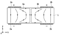
- FIG. 1 is a diagram showing a configuration of a variable focus lens according to an embodiment of the present invention.
- FIG. 2 is a diagram for explaining the principle of the variable focus lens according to the present embodiment.
- FIG. 3 is a diagram showing an electric field component and a refractive index distribution inside the substrate of the variable focus lens.
- FIG. 4 is a diagram illustrating a configuration of the variable focus lens according to the first embodiment.
- FIG. 5A is a diagram illustrating an optical path length modulation distribution of the variable focus lens according to the second example.
- FIG. 5B is a diagram illustrating an optical path length modulation distribution of the variable focus lens according to the second example.
- FIG. 6 is a diagram illustrating the deviation between the optical path length modulation and the ideal quadratic curve in the variable focus lens according to the second example.
- variable focus lens of this embodiment is composed of an electro-optic material and an electrode attached thereto. By utilizing the electro-optic effect, a much faster response speed can be obtained as compared with a conventional variable focus lens.
- FIG. 1 shows a configuration of a variable focus lens according to an embodiment of the present invention.
- a pair of upper electrodes 2a, 2b and lower electrodes 3a, 3b are respectively formed on the upper surface (light incident surface) and the lower surface (light emitting surface) of the substrate 1 obtained by processing the electro-optic material into a plate shape.
- the upper electrodes 2a and 2b are set to the same potential, and the lower electrodes 3a and 3b are set to the same potential.
- the optical axis is set in the y-axis direction so that light passes through the gap between the pair of electrodes having the same potential.
- Each of the upper electrodes 2a and 2b is formed so that sides facing each other across a gap through which light passes is parallel to the z axis, and the interval between the two sides is A.
- the lower electrodes 3a and 3b have the same configuration, and the positions of the opposing sides coincide with the opposing sides of the upper electrodes 2a and 2b in the x-axis direction, that is, with the substrate 1 in between.
- the thickness of the substrate 1 is T.
- a voltage can be applied from the upper electrode 2 to the lower electrode pair 3 or vice versa.
- the electro-optic material is preferably an oxide single crystal material having inversion symmetry.
- the inversion symmetry will be described later in detail. Details of the electrodes will be described later.
- variable focus lens The principle of the variable focus lens according to the present embodiment will be described with reference to FIG.
- a positive voltage is applied to the upper electrodes 2a and 2b, and a negative voltage is applied to the lower electrodes 3a and 3b.
- an electric field is generated between the vertically facing electrodes in a state of facing from top to bottom.
- the electric field is generated not only between the upper and lower electrodes but also around it, and also in a portion where light is transmitted. Due to the protruding electric field, an electro-optic effect is generated in the substrate 1 which is an electro-optic material, and the refractive index of the portion through which light is transmitted is modulated.
- the electro-optic material generally has a relative dielectric constant sufficiently larger than 1. For this reason, the electric field lines of the electric field inside the substrate 1 are nearly parallel to the substrate surface near the surface (see reference numerals 4a and 4b). The electric lines of force 4a traveling rightward from the upper electrode 2a proceed almost parallel to the upper surface of the substrate 1 after leaving the upper electrode 2a. On the other hand, the electric lines of force 4b traveling leftward from the upper electrode 2b also proceed almost parallel to the upper surface of the substrate 1 after leaving the upper electrode 2b.
- the electric lines of force 4a and 4b collide with each other at the center of the upper electrodes 2a and 2b, the electric lines of force 4a and 4b are largely turned from there and proceed downward.
- the electric lines of force 4a and 4b then reach the lower surface, change their direction greatly, proceed in opposite directions, and proceed to the lower electrodes 3a and 3b, respectively.
- the electric lines of force traveling near the surface inside the substrate 1 are bent sharply in the gap between the pair of electrodes having the same potential, so that the electric field greatly changes in the bent portion. That is, the refractive index is modulated by changing the electric field around the optical axis where light is transmitted.
- FIG. 3 shows the electric field component and the refractive index distribution inside the substrate.
- 3 (a) shows the x-axis direction in the vicinity of the upper surface of the substrate 1, the distribution of the electric field component E x.
- the horizontal axis represents the position in the x-axis direction of the portion where light between the pair of electrodes having the same potential is transmitted. Since the direction of the electric lines of force differs 180 degrees between the left and right with the central portion as the boundary, this distribution is obtained.
- FIG. 3B similarly shows the distribution of the electric field component E y in the y-axis direction at each position in the x-axis direction.
- the electric field component E y has the same sign, but its absolute value is small at the center and increases as it approaches the electrode.
- Such an electric field distribution modulates the refractive index in the x-axis direction.
- FIG. 3C shows a refractive index when light having an optical electric field incident in the z direction is incident using potassium tantalate niobate (KTa 1-x Nb x O 3 , hereinafter referred to as KTN) as an electrooptic material.
- KTN potassium tantalate niobate
- variable focus lenses having the configuration shown in FIGS. 1 and 2 are prepared and arranged so that the optical axes of the portions through which the light passes are aligned.
- the two variable focus lenses By arranging the two variable focus lenses at an angle of 90 degrees with respect to the optical axis as a center, by performing condensing or diverging in two directions, a function equivalent to a spherical lens can be realized.
- the electro-optic effect includes several different-order electro-optic effects, but in general, the first-order electro-optic effect (hereinafter referred to as Pockels effect) and the second-order electro-optic effect (hereinafter referred to as Kerr effect). Is used).
- a material having a secondary electro-optic effect (Kerr effect) in which refractive index modulation proportional to the square of the electric field occurs is preferable.
- Kerr effect as shown in FIG. 3, the refractive index distribution ⁇ n is because it does not depend on the sign of the electric field component E x, become suitable symmetrical shape as a lens.
- a single crystal having inversion symmetry refers to a crystal in which the arrangement of atoms is exactly the same as the original arrangement of atoms when the arrangement of atoms is inverted in the x, y, z coordinate system around a certain origin. Note that when a material having spontaneous polarization is inverted on the coordinate axis, the direction of spontaneous polarization is inverted, and thus such a crystal material does not have inversion symmetry. On the other hand, a single crystal having inversion symmetry has no Pockels effect, and the Kerr effect is the lowest order electro-optic effect. Therefore, among crystal materials having an electro-optic effect, a single crystal having inversion symmetry is desirable.
- the magnitude of the electric field inside the crystal is proportional to the voltage applied to the electrode. Also, since the refractive index modulation is proportional to the square of the electric field, the magnitude of the refractive index modulation is proportional to the square of the voltage. Thereby, the focal length of the concave lens can be controlled by the voltage. Although it has been described here that it functions as a concave lens, the sign of the electro-optic coefficient differs depending on the material and light polarization, so that a convex lens can also be realized.
- the electro-optic material is preferably a single crystal material having a perovskite crystal structure. This is because the perovskite single crystal material has a cubic phase having reversal symmetry in the use state if the use temperature is appropriately selected, and does not have the Pockels effect in this cubic phase. For example, even the most well-known barium titanate (BaTiO 3 , hereinafter referred to as BT) may exceed the temperature at which the phase transition from the tetragonal phase to the cubic phase (hereinafter referred to as the phase transition temperature) occurs at around 120 ° C. For example, it becomes a cubic phase and exhibits the Kerr effect.
- BaTiO 3 barium titanate
- the single crystal material mainly composed of KTN has more preferable characteristics.
- BT has a predetermined phase transition temperature, whereas KTN can select a phase transition temperature depending on the composition ratio of tantalum and niobium.
- the phase transition temperature can be set near room temperature.
- KTN has a cubic phase at a temperature higher than the phase transition temperature, has inversion symmetry, and has a large Kerr effect. Even in the same cubic phase, the Kerr effect becomes overwhelmingly closer to the phase transition temperature. For this reason, setting the phase transition temperature around room temperature is very important for easily realizing a large Kerr effect.
- the main component of the crystal is composed of groups Ia and Va in the periodic table, group Ia is potassium, and group Va contains at least one of niobium and tantalum. Can be used. Furthermore, it is possible to include one or more members of Group Ia of the periodic table excluding potassium as an additive impurity, for example, lithium, or Group IIa.
- a cubic phase KLTN K 1-y Li y Ta 1-x Nb x O 3 , 0 ⁇ x ⁇ 1, 0 ⁇ y ⁇ 1) crystal having a large Kerr effect may be used.
- the dielectric constant increases rapidly when the operating temperature is brought close to the phase transition temperature.
- the electro-optic effect is increased.
- the dielectric constant is high, the bending of the electric lines of force shown in FIG. 2 becomes more abrupt and the lens effect increases.
- the focal length is 1 m or less due to the synergistic effect of combining the large electro-optic effect and the bending of the electric field lines.
- the refractive index modulation of KTN varies depending on the relationship between the direction of the applied electric field and the direction of the optical electric field, as in other electro-optic crystals.
- the refractive index modulation [Delta] n x and [Delta] n z where light feel
- n 0 is the refractive index before modulation.
- s 11 and s 12 are electro-optic coefficients. S 11 is positive, whereas s 12 has a negative value, and the absolute value is larger in s 11 . Because of this feature, the function changes completely depending on the polarization state of the incident light, a convex lens when the direction of the optical electric field is the x direction, and a concave lens when the direction of the optical field is the z direction.
- Electrode material When a high voltage is applied to the electro-optic material, charges are injected from the electrodes, and space charges can be generated in the crystal. This space charge causes an electric field to be tilted in the direction of voltage application, so that the refractive index is also tilted.
- the carrier injection efficiency injected from the electrode should be small.
- the work function of the electrode material is preferably 5.0 eV or more.
- Electrode material having a work function of 5.0 eV or more Co (5.0), Ge (5.0), Au (5.1), Pd (5.12), Ni (5.15), Ir (5.27), Pt (5.65), Se (5.9) can be used.
- Figures in parentheses indicate work functions (eV).
- the work function of the electrode material is preferably less than 5.0 eV in order to suppress the injection of holes.
- Ti (3.84) or the like can be used as an electrode material having a work function of 5.0 eV or more. Since the Ti single-layer electrode is oxidized and becomes high resistance, generally, the Ti layer and the electro-optic crystal are bonded using an electrode in which Ti / Pt / Au is laminated. Furthermore, transparent electrodes such as ITO (Indium Tin Oxide) and ZnO can also be used.
- FIG. 4 shows a configuration of the variable focus lens according to the first example.
- a pair of upper electrodes 12a and 12b and a pair of lower electrodes 13a and 13b are formed on the upper and lower surfaces of the substrate 11 obtained by processing the electro-optic material into a plate shape.
- the relative dielectric constant at this temperature is 20,000.
- Each of the upper electrodes 12a and 12b and the lower electrodes 13a and 13b has a square shape of 0.6 mm ⁇ 2.6 mm and is formed by depositing platinum (Pt).
- the opposing sides are arranged in parallel with a gap through which light passes, and the distance A between these two sides is 1.4 mm.
- the collimated laser light is incident on the gap between the upper electrodes 12a and 12b while the temperature of the variable focus lens of Example 1 is controlled at 40 ° C.
- the polarization of light is a straight line, and the direction of the oscillating electric field is the z-axis direction.
- a voltage of 500 V is applied between the upper and lower electrodes, the light emitted from between the lower electrodes 13a and 13b spreads in the x-axis direction and functions as a cylindrical concave lens.
- the focal length is 25 cm.
- the applied voltage is 250 V
- the spread becomes small and the focal length becomes about 1 m. That is, the focal length can be changed by the applied voltage. Since changing the focal length only changes the applied voltage, the response time is 1 ⁇ s or less, which is an improvement of three orders of magnitude or more compared to the response time of the conventional variable focus lens.
- the measurement is performed by rotating the polarized light by 90 degrees while maintaining the traveling direction of the light. That is, the direction of the oscillating electric field of light is the x-axis direction. In this case, it functions as a convex lens.
- the applied voltage is 500 V
- the focal length is 19 cm, and the focal length can be changed by the applied voltage.
- the characteristic of the lens is expressed by optical path length modulation that the light receives by passing through the substrate 1.
- the optical path length modulation ⁇ s is obtained by integrating the refractive index modulation ⁇ n over the path through the electro-optic material. As described above, since the refractive index modulation is a function of x and y, this is assumed to be ⁇ n (x, y). The refractive index modulation ⁇ n does not depend on z. Since the variable focus lens according to the present embodiment propagates light in the y-axis direction, the optical path length modulation ⁇ s is
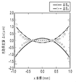
- FIGS. 5A and 5B show optical path length modulation distributions of the variable focus lens according to Example 2.
- the horizontal axis represents the position in the x-axis direction, and the origin is the center of the portion through which light is transmitted.
- the vertical axis represents the optical path length modulation ⁇ s.
- the optical path length modulation ( ⁇ Sx) when the optical electric field is directed in the x-axis direction is convex upward, indicating that it functions as a convex lens.
- the optical path length modulation ( ⁇ Sz) when the optical electric field is directed in the z-axis direction is convex downward, indicating that it functions as a concave lens.
- FIG. 5A and 5B show the results of fitting to a quadratic curve. Ideally, it would be desirable to follow this quadratic curve, but in each case there is a slight deviation. Furthermore, FIG. 5A has a larger deviation from the quadratic curve than FIG. 5B. This is because the electric lines of force that spread from each electrode to the portion where light is transmitted spread only within a range determined by the thickness T of the substrate 1. That is, when the same voltage is applied between the upper electrode and the lower electrode, if the distance A between the upper electrode and the lower electrode is too wide (in the case of FIG. 5A), the electric lines of force reach the center of the portion where the light is transmitted. This is because the electro-optic effect is reduced and the refractive index modulation is also reduced.
- FIG. 6 shows the deviation between the optical path length modulation and the ideal quadratic curve in the variable focus lens according to Example 2.
- the vertical axis represents the peak / peak value of the deviation between the actual optical path length modulation ⁇ s and the ideal quadratic curve. That is, the optical path length modulation (plots ⁇ and ⁇ in FIGS. 5A and 5B) is determined by determining the interval A and the thickness T, and the fitting shown in FIGS. 5A and 5B is performed. In this range, the minimum value and the maximum value of the deviation amount are obtained, and the deflection width is shown as the peak / peak value.
- the guideline for the amount of deviation of the optical path length modulation ⁇ s is about the light wavelength (approximately 1 ⁇ m), so it is desirable that R be 1.5 or less.
- the upper electrodes 12a and 12b are shown as independent electrodes. However, as long as unnecessary disturbance is not given to the electric field distribution inside the substrate 11, the upper electrodes 12a and 12b are coupled on the upper surface of the substrate 11 or by other methods. It may be a combined electrode. Similarly, the lower electrodes 13a and 13b may be combined electrodes as long as the electric field distribution inside the substrate 11 is not disturbed.
- the opposing sides of the upper electrodes 12a and 12b and the lower electrodes 13a and 13b are coincident in the x-axis direction with the substrate 11 interposed therebetween, but are not necessarily coincident with each other. What is necessary is just to be parallel.
- the upper electrode and the lower electrode are shown as squares, but the shape excluding the opposite sides across the gap through which light passes can be any shape since it does not affect the lens action. Further, from the outer extension of the light transmitting region, about the same distance as the electrode interval A or the substrate thickness T, or more in the z-axis direction, even on the sides facing each other with a gap therebetween, It may be any shape.
Landscapes
- Physics & Mathematics (AREA)
- Nonlinear Science (AREA)
- General Physics & Mathematics (AREA)
- Optics & Photonics (AREA)
- Optical Modulation, Optical Deflection, Nonlinear Optics, Optical Demodulation, Optical Logic Elements (AREA)
- Liquid Crystal (AREA)
Abstract
Priority Applications (4)
| Application Number | Priority Date | Filing Date | Title |
|---|---|---|---|
| US12/808,105 US8014061B2 (en) | 2007-12-28 | 2008-12-26 | Variable-focal length lens |
| EP08867509.5A EP2233966B1 (fr) | 2007-12-28 | 2008-12-26 | Methode pour focaliser ou defocaliser la lumiere en utilisant une lentille a focale variable |
| CN2008801224619A CN101910914B (zh) | 2007-12-28 | 2008-12-26 | 变焦透镜 |
| JP2009548120A JP5406046B2 (ja) | 2007-12-28 | 2008-12-26 | 可変焦点レンズ |
Applications Claiming Priority (2)
| Application Number | Priority Date | Filing Date | Title |
|---|---|---|---|
| JP2007341067 | 2007-12-28 | ||
| JP2007-341067 | 2007-12-28 |
Publications (1)
| Publication Number | Publication Date |
|---|---|
| WO2009084692A1 true WO2009084692A1 (fr) | 2009-07-09 |
Family
ID=40824405
Family Applications (1)
| Application Number | Title | Priority Date | Filing Date |
|---|---|---|---|
| PCT/JP2008/073863 Ceased WO2009084692A1 (fr) | 2007-12-28 | 2008-12-26 | Lentille à foyer variable |
Country Status (5)
| Country | Link |
|---|---|
| US (1) | US8014061B2 (fr) |
| EP (1) | EP2233966B1 (fr) |
| JP (1) | JP5406046B2 (fr) |
| CN (1) | CN101910914B (fr) |
| WO (1) | WO2009084692A1 (fr) |
Cited By (7)
| Publication number | Priority date | Publication date | Assignee | Title |
|---|---|---|---|---|
| WO2010143449A1 (fr) * | 2009-06-12 | 2010-12-16 | 日本電信電話株式会社 | Lentille à foyer variable et microscope |
| CN101963699A (zh) * | 2010-09-08 | 2011-02-02 | 华中科技大学 | 一种基于ktn晶体的变焦透镜的轴向随机扫描方法 |
| JP2012004514A (ja) * | 2010-06-21 | 2012-01-05 | Nippon Telegr & Teleph Corp <Ntt> | 波長可変レーザ光源 |
| JP2012042900A (ja) * | 2010-08-23 | 2012-03-01 | Nippon Telegr & Teleph Corp <Ntt> | 偏光無依存可変焦点レンズ |
| JP2012042688A (ja) * | 2010-08-18 | 2012-03-01 | Nippon Telegr & Teleph Corp <Ntt> | 可変焦点レンズ |
| JP2014052532A (ja) * | 2012-09-07 | 2014-03-20 | Saitama Univ | 非線形光学顕微鏡 |
| JP2017506666A (ja) * | 2014-02-28 | 2017-03-09 | テンシャ セラピューティクス,インコーポレイテッド | 高インスリン血症に関連した症状の処置 |
Families Citing this family (4)
| Publication number | Priority date | Publication date | Assignee | Title |
|---|---|---|---|---|
| JP5230554B2 (ja) * | 2009-07-23 | 2013-07-10 | キヤノン株式会社 | 光学機器 |
| US9442285B2 (en) | 2011-01-14 | 2016-09-13 | The Board Of Trustees Of The University Of Illinois | Optical component array having adjustable curvature |
| WO2012158709A1 (fr) | 2011-05-16 | 2012-11-22 | The Board Of Trustees Of The University Of Illinois | Barrettes de del à gestion thermique assemblées par impression |
| KR102266468B1 (ko) * | 2014-07-18 | 2021-06-17 | 삼성전자주식회사 | 초점 제어 방법 및 그 전자 장치 |
Citations (5)
| Publication number | Priority date | Publication date | Assignee | Title |
|---|---|---|---|---|
| JPH1164817A (ja) | 1997-06-10 | 1999-03-05 | Olympus Optical Co Ltd | 可変焦点レンズ、可変焦点回折光学素子、および可変偏角プリズム |
| JP2001194690A (ja) * | 2000-01-14 | 2001-07-19 | Minolta Co Ltd | 焦点位置可変空間変調デバイス |
| WO2006137408A1 (fr) * | 2005-06-20 | 2006-12-28 | Nippon Telegraph And Telephone Corporation | Élément électro-optique |
| JP2007310104A (ja) * | 2006-05-17 | 2007-11-29 | Nippon Telegr & Teleph Corp <Ntt> | 電気光学素子およびその製造方法 |
| JP2009014793A (ja) * | 2007-06-29 | 2009-01-22 | Sunx Ltd | 焦点距離調整装置、レーザ加工装置、レーザ変位計及び電気光学素子 |
Family Cites Families (17)
| Publication number | Priority date | Publication date | Assignee | Title |
|---|---|---|---|---|
| BE552987A (fr) * | 1955-12-07 | |||
| US3357771A (en) * | 1963-10-01 | 1967-12-12 | Gen Telephone & Elect | Light beam deflector employing electro-optic crystal |
| US3460884A (en) * | 1965-06-21 | 1969-08-12 | Ibm | Electro-optical devices utilizing the stark-shift phenomenon |
| US4181399A (en) * | 1978-01-03 | 1980-01-01 | Sperry Rand Corporation | Optical internal reflectance switchable coupler |
| US4466703A (en) * | 1981-03-24 | 1984-08-21 | Canon Kabushiki Kaisha | Variable-focal-length lens using an electrooptic effect |
| JPH01230017A (ja) * | 1988-03-10 | 1989-09-13 | Ricoh Co Ltd | 光学素子 |
| US5272561A (en) * | 1989-01-24 | 1993-12-21 | Ricoh Company, Ltd. | Electrooptic device |
| US5124835A (en) * | 1989-06-21 | 1992-06-23 | Ricoh Company, Ltd. | Optical scanning apparatus |
| US5221989A (en) * | 1991-11-13 | 1993-06-22 | Northrop Corporation | Longitudinal plzt spatial light modulator |
| US5301201A (en) * | 1993-03-01 | 1994-04-05 | At&T Bell Laboratories | Article comprising a tunable semiconductor laser |
| JPH09146128A (ja) * | 1995-11-24 | 1997-06-06 | Sony Corp | 電気光学素子 |
| JP3734563B2 (ja) * | 1996-03-26 | 2006-01-11 | 株式会社リコー | 電気光学レンズ |
| US6577434B2 (en) | 2000-01-14 | 2003-06-10 | Minolta Co., Ltd. | Variable focal position spatial modulation device |
| JP3935810B2 (ja) * | 2002-09-27 | 2007-06-27 | シャープ株式会社 | 光路変換デバイス |
| EP2312351B1 (fr) * | 2003-07-16 | 2018-12-05 | Nippon Telegraph And Telephone Corporation | Guide d'onde optique |
| US6859333B1 (en) * | 2004-01-27 | 2005-02-22 | Research Foundation Of The University Of Central Florida | Adaptive liquid crystal lenses |
| CN101153945A (zh) * | 2006-09-29 | 2008-04-02 | 鸿富锦精密工业(深圳)有限公司 | 镜头模组 |
-
2008
- 2008-12-26 WO PCT/JP2008/073863 patent/WO2009084692A1/fr not_active Ceased
- 2008-12-26 CN CN2008801224619A patent/CN101910914B/zh active Active
- 2008-12-26 EP EP08867509.5A patent/EP2233966B1/fr active Active
- 2008-12-26 JP JP2009548120A patent/JP5406046B2/ja active Active
- 2008-12-26 US US12/808,105 patent/US8014061B2/en active Active
Patent Citations (5)
| Publication number | Priority date | Publication date | Assignee | Title |
|---|---|---|---|---|
| JPH1164817A (ja) | 1997-06-10 | 1999-03-05 | Olympus Optical Co Ltd | 可変焦点レンズ、可変焦点回折光学素子、および可変偏角プリズム |
| JP2001194690A (ja) * | 2000-01-14 | 2001-07-19 | Minolta Co Ltd | 焦点位置可変空間変調デバイス |
| WO2006137408A1 (fr) * | 2005-06-20 | 2006-12-28 | Nippon Telegraph And Telephone Corporation | Élément électro-optique |
| JP2007310104A (ja) * | 2006-05-17 | 2007-11-29 | Nippon Telegr & Teleph Corp <Ntt> | 電気光学素子およびその製造方法 |
| JP2009014793A (ja) * | 2007-06-29 | 2009-01-22 | Sunx Ltd | 焦点距離調整装置、レーザ加工装置、レーザ変位計及び電気光学素子 |
Non-Patent Citations (2)
| Title |
|---|
| See also references of EP2233966A4 * |
| TAKUYA KANEKO: "Optical Microscope Expanded Depth of Field using Dynamic Focusing Lens for Micro Parts Assembling", DENSO TECHNICAL REVIEW, vol. 3, no. 1, 1998, pages 52 - 58 |
Cited By (8)
| Publication number | Priority date | Publication date | Assignee | Title |
|---|---|---|---|---|
| WO2010143449A1 (fr) * | 2009-06-12 | 2010-12-16 | 日本電信電話株式会社 | Lentille à foyer variable et microscope |
| US8773749B2 (en) | 2009-06-12 | 2014-07-08 | Nippon Telegraph And Telephone Corporation | Variable focusing lens and microscope |
| JP2012004514A (ja) * | 2010-06-21 | 2012-01-05 | Nippon Telegr & Teleph Corp <Ntt> | 波長可変レーザ光源 |
| JP2012042688A (ja) * | 2010-08-18 | 2012-03-01 | Nippon Telegr & Teleph Corp <Ntt> | 可変焦点レンズ |
| JP2012042900A (ja) * | 2010-08-23 | 2012-03-01 | Nippon Telegr & Teleph Corp <Ntt> | 偏光無依存可変焦点レンズ |
| CN101963699A (zh) * | 2010-09-08 | 2011-02-02 | 华中科技大学 | 一种基于ktn晶体的变焦透镜的轴向随机扫描方法 |
| JP2014052532A (ja) * | 2012-09-07 | 2014-03-20 | Saitama Univ | 非線形光学顕微鏡 |
| JP2017506666A (ja) * | 2014-02-28 | 2017-03-09 | テンシャ セラピューティクス,インコーポレイテッド | 高インスリン血症に関連した症状の処置 |
Also Published As
| Publication number | Publication date |
|---|---|
| US20100290104A1 (en) | 2010-11-18 |
| EP2233966B1 (fr) | 2013-10-23 |
| EP2233966A4 (fr) | 2011-01-12 |
| EP2233966A1 (fr) | 2010-09-29 |
| US8014061B2 (en) | 2011-09-06 |
| JPWO2009084692A1 (ja) | 2011-05-19 |
| CN101910914B (zh) | 2013-03-27 |
| JP5406046B2 (ja) | 2014-02-05 |
| CN101910914A (zh) | 2010-12-08 |
Similar Documents
| Publication | Publication Date | Title |
|---|---|---|
| JP5406046B2 (ja) | 可変焦点レンズ | |
| JP5426500B2 (ja) | 偏光無依存可変焦点レンズ | |
| JP4057597B2 (ja) | 光学素子 | |
| CN102449536B (zh) | 变焦透镜及显微镜 | |
| JP2010026079A (ja) | 光デバイス | |
| JP5411089B2 (ja) | 可変焦点レンズ | |
| JP2014098790A (ja) | 光ピンセット装置 | |
| US9291874B2 (en) | Optical deflection element and optical deflection device | |
| JP5432044B2 (ja) | 可変焦点レンズ | |
| JP2014202786A (ja) | 可変焦点レンズ | |
| US10788728B2 (en) | Light beam steering using electro-optical and conductive materials | |
| JP5069267B2 (ja) | 可変焦点レンズ | |
| JP5069266B2 (ja) | 可変焦点レンズ | |
| JP5161156B2 (ja) | 可変焦点レンズ | |
| JP2014026229A (ja) | 可変焦点レンズ | |
| JP6010510B2 (ja) | 可変焦点ミラー | |
| JP6611052B2 (ja) | 可変焦点レンズ | |
| JP6259360B2 (ja) | 可変焦点レンズ | |
| JP6346572B2 (ja) | 可変焦点レンズ | |
| JP6335111B2 (ja) | 可変焦点レンズ | |
| JP2018101109A (ja) | 可変焦点レンズ |
Legal Events
| Date | Code | Title | Description |
|---|---|---|---|
| WWE | Wipo information: entry into national phase |
Ref document number: 200880122461.9 Country of ref document: CN |
|
| 121 | Ep: the epo has been informed by wipo that ep was designated in this application |
Ref document number: 08867509 Country of ref document: EP Kind code of ref document: A1 |
|
| WWE | Wipo information: entry into national phase |
Ref document number: 2009548120 Country of ref document: JP |
|
| WWE | Wipo information: entry into national phase |
Ref document number: 12808105 Country of ref document: US |
|
| WWE | Wipo information: entry into national phase |
Ref document number: 2008867509 Country of ref document: EP |
|
| NENP | Non-entry into the national phase |
Ref country code: DE |