WO2009087705A1 - アクティブマトリクス基板及び液晶表示装置 - Google Patents
アクティブマトリクス基板及び液晶表示装置 Download PDFInfo
- Publication number
- WO2009087705A1 WO2009087705A1 PCT/JP2008/002470 JP2008002470W WO2009087705A1 WO 2009087705 A1 WO2009087705 A1 WO 2009087705A1 JP 2008002470 W JP2008002470 W JP 2008002470W WO 2009087705 A1 WO2009087705 A1 WO 2009087705A1
- Authority
- WO
- WIPO (PCT)
- Prior art keywords
- active matrix
- matrix substrate
- pixel electrodes
- pixel electrode
- liquid crystal
- Prior art date
- Legal status (The legal status is an assumption and is not a legal conclusion. Google has not performed a legal analysis and makes no representation as to the accuracy of the status listed.)
- Ceased
Links
Images




Classifications
-
- G—PHYSICS
- G02—OPTICS
- G02F—OPTICAL DEVICES OR ARRANGEMENTS FOR THE CONTROL OF LIGHT BY MODIFICATION OF THE OPTICAL PROPERTIES OF THE MEDIA OF THE ELEMENTS INVOLVED THEREIN; NON-LINEAR OPTICS; FREQUENCY-CHANGING OF LIGHT; OPTICAL LOGIC ELEMENTS; OPTICAL ANALOGUE/DIGITAL CONVERTERS
- G02F1/00—Devices or arrangements for the control of the intensity, colour, phase, polarisation or direction of light arriving from an independent light source, e.g. switching, gating or modulating; Non-linear optics
- G02F1/01—Devices or arrangements for the control of the intensity, colour, phase, polarisation or direction of light arriving from an independent light source, e.g. switching, gating or modulating; Non-linear optics for the control of the intensity, phase, polarisation or colour
- G02F1/13—Devices or arrangements for the control of the intensity, colour, phase, polarisation or direction of light arriving from an independent light source, e.g. switching, gating or modulating; Non-linear optics for the control of the intensity, phase, polarisation or colour based on liquid crystals, e.g. single liquid crystal display cells
- G02F1/133—Constructional arrangements; Operation of liquid crystal cells; Circuit arrangements
- G02F1/136—Liquid crystal cells structurally associated with a semi-conducting layer or substrate, e.g. cells forming part of an integrated circuit
- G02F1/1362—Active matrix addressed cells
- G02F1/136286—Wiring, e.g. gate line, drain line
-
- G—PHYSICS
- G02—OPTICS
- G02F—OPTICAL DEVICES OR ARRANGEMENTS FOR THE CONTROL OF LIGHT BY MODIFICATION OF THE OPTICAL PROPERTIES OF THE MEDIA OF THE ELEMENTS INVOLVED THEREIN; NON-LINEAR OPTICS; FREQUENCY-CHANGING OF LIGHT; OPTICAL LOGIC ELEMENTS; OPTICAL ANALOGUE/DIGITAL CONVERTERS
- G02F1/00—Devices or arrangements for the control of the intensity, colour, phase, polarisation or direction of light arriving from an independent light source, e.g. switching, gating or modulating; Non-linear optics
- G02F1/01—Devices or arrangements for the control of the intensity, colour, phase, polarisation or direction of light arriving from an independent light source, e.g. switching, gating or modulating; Non-linear optics for the control of the intensity, phase, polarisation or colour
- G02F1/13—Devices or arrangements for the control of the intensity, colour, phase, polarisation or direction of light arriving from an independent light source, e.g. switching, gating or modulating; Non-linear optics for the control of the intensity, phase, polarisation or colour based on liquid crystals, e.g. single liquid crystal display cells
- G02F1/133—Constructional arrangements; Operation of liquid crystal cells; Circuit arrangements
- G02F1/136—Liquid crystal cells structurally associated with a semi-conducting layer or substrate, e.g. cells forming part of an integrated circuit
- G02F1/13606—Liquid crystal cells structurally associated with a semi-conducting layer or substrate, e.g. cells forming part of an integrated circuit having means for reducing parasitic capacitance
Definitions
- the present invention relates to an active matrix substrate and a liquid crystal display device.
- liquid crystal display devices have been widely used as displays for televisions, personal computers, mobile phones, PDAs (Personal Digital Assistants), etc., taking advantage of the thin and low power consumption characteristics.
- An active matrix driving liquid crystal display device includes an active matrix substrate on which a plurality of pixel electrodes and TFTs (Thin-Film-Transistors) are formed, a counter substrate on which the common electrode is formed so as to face the active matrix substrate, and these A liquid crystal layer sealed inside a frame-shaped sealing material is provided between the two substrates, and the display unit includes a plurality of pixels and displays an image.
- TFTs Thin-Film-Transistors
- FIG. 11 is a plan view schematically showing an enlarged part of an active matrix substrate in a conventional delta-alignment liquid crystal display device.
- the wirings 103 and 104 and the TFT 105 are shown through the insulating film 106.
- a plurality of pixel electrodes 101 constituting each pixel are provided in a delta arrangement on an active matrix substrate in a delta arrangement liquid crystal display device.
- Each pixel electrode 101 defines a plurality of linearly aligned rows 102, and is provided with a half-pitch shift in the row direction (lateral direction in the figure) in each adjacent row 102a, 102b.
- each pixel electrode 101 a plurality of gate lines 103 provided so as to extend in parallel with each other along each row 102a, 102b, and a direction intersecting with each gate line 103 while being alternately bent left and right in the figure.
- a plurality of source lines 104 provided so as to extend in the direction is formed.
- a TFT 105 is connected to each pixel electrode 101.
- Each TFT 105 is laminated with an insulating film 106, and a drain electrode 107 is connected to the pixel electrode 101 through a contact hole 106 a formed in the insulating film 106.
- Each of these TFTs 105 is provided near the intersection of each gate line 103 and each source line 104 from the viewpoint of increasing the aperture ratio of each pixel.
- Each source line 104 is connected to each of the plurality of first linear portions 104a provided so as to extend along the left side of each pixel electrode 101 in the drawing, and to each of the first linear portions 104a.
- the electrode 101 has a plurality of second linear portions 104b provided so as to extend to the middle portion of the sides along the upper and lower sides of the electrode 101 in the drawing.
- Each second linear portion 104b provided along each source line 104 has a plurality of second linear portions 104b extending along the upper side or the lower side of each pixel electrode 101 at one end thereof.
- a protruding portion 104c is provided.
- the TFTs 105 are alternately connected to the protrusions 104 c and the second linear portions 104 b along the source lines 104.
- the active matrix substrate has a non-inverted structure in which the position of the TFT 105 connected to each pixel electrode 101 is the same with respect to each pixel electrode 101.
- parasitic capacitance is generated between each pixel electrode and the source line.
- the parasitic capacitance increases as the distance between the pixel electrode and the source line decreases, and increases as the length of the source line along the pixel electrode increases.
- This parasitic capacitance reduces the voltage applied between the pixel electrode and the common electrode in accordance with the size of the parasitic capacitance, thereby reducing the transmittance of the liquid crystal layer.
- each source line 104 in each source line 104, the upper side of each pixel electrode 101 in one row 102a in adjacent rows 102a and 102b.
- the portion 104d along the side of the lower side and the portion 104e along the lower side of the drawing, and the portion 104f along the side of the upper side of the pixel electrode 101 in the other row 102b and the drawing.
- the portion 104g along the middle and lower side.
- each source line 104 the portion 104d along the upper side in the drawing and the pixel electrode 101 of the one row 102a is longer than the portion 104e along the lower side in the drawing by the protruding portion 104c.
- the portion 104g along the lower side in the figure of each pixel electrode 101 in the other row 102b is also longer than the portion 104f along the upper side in the figure by the protruding portion 104c.
- the active matrix substrate has each pixel electrode 101 and each source line 104 as desired so that the distance between each pixel electrode 101 and each source line 104 is constant on both sides in the vertical direction in the figure.
- the parasitic capacitance between each pixel electrode 101 and the source line 104 is designed to be the same.
- each pixel in one row 102a in adjacent rows 102a and 102b when the formation position of each pixel electrode 101 with respect to each source line 104 is shifted, for example, in the upper left direction in the figure, each pixel in one row 102a in adjacent rows 102a and 102b.
- the electrode 101 approaches the relatively long portion 104d of each source line 104 and moves away from the relatively short portion 104e.
- each pixel electrode 101 in the other row 102b approaches the relatively short portion 104f in each source line 104 and moves away from the relatively long portion 104g. This causes a difference in parasitic capacitance between each pixel electrode 101 and the source line 104 in the adjacent rows 102a and 102b.
- the present invention has been made in view of such various points, and an object of the present invention is to provide a space between each pixel electrode and a source line in adjacent rows of a plurality of pixel electrodes provided in a delta arrangement. This is to suppress the difference in parasitic capacitance.
- a plurality of second electrodes are provided so as to extend while alternately bending between a plurality of pixel electrodes provided in a delta arrangement, and extend along the side of each pixel electrode.
- a plurality of source lines each having a first linear portion and a plurality of second linear portions connected to the first linear portions and extending to the middle portion of the side along the side of each pixel electrode are
- a plurality of protrusions extending from one end of the two linear portions along the side of each pixel electrode are provided.
- an active matrix substrate includes a plurality of pixel electrodes provided in a delta arrangement, and a plurality of gate lines provided in a line so as to extend in parallel with each other between the pixel electrodes.
- a plurality of source lines provided so as to extend in parallel with each other in a direction intersecting with each gate line while being alternately bent between the pixel electrodes, and a plurality of thin film transistors respectively connected to the pixel electrodes.
- Each source line includes a plurality of first linear portions provided so as to extend along the side sides of the pixel electrodes, and the side sides of the pixel electrodes connected to the first linear portions.
- a plurality of second linear portions provided so as to extend to an intermediate portion of the side edge, and provided so as to extend along one side edge of each pixel electrode from one end of each second linear portion.
- Each of the above-described thin film transistors. Njisuta is along the source lines are alternately connected to each of the above first linear portion or each of the second linear portion and the respective projecting portions.
- the protrusions are formed with the same length.
- the liquid crystal display device includes the active matrix substrate, a counter substrate disposed to face the active matrix substrate, a liquid crystal layer provided between the active matrix substrate and the counter substrate, Have
- the plurality of first linear portions are provided so as to extend while being alternately bent between the plurality of pixel electrodes provided in the delta arrangement, and extend along the side edges of the pixel electrode.
- a plurality of source lines having a plurality of second linear portions connected to each first linear portion and extending to the middle portion of the side along the side of each pixel electrode are connected to each of the second linear portions. Since each of the source lines has a plurality of protrusions extending from one end along the side of each pixel electrode, the length of the portion along each pixel electrode on each side of each pixel electrode in the row direction of each row The difference of becomes smaller. Thereby, even if the formation positions of the pixel electrodes and the source lines are shifted, the difference in parasitic capacitance between the respective pixel electrodes and the source lines is suppressed in adjacent rows.
- the protrusions are formed to have the same length, there is no difference in the lengths of the portions along the pixel electrodes on both sides in the row direction of the pixel electrodes in the source lines. In the adjacent rows, the difference in parasitic capacitance between each pixel electrode and the source line is suppressed as much as possible.
- the liquid crystal display device includes the active matrix substrate, a counter substrate disposed to face the active matrix substrate, and a liquid crystal layer provided between the two substrates. Therefore, even if the formation position of each pixel electrode and each source line is shifted, the difference in parasitic capacitance between each pixel electrode and the source line is suppressed in adjacent rows. And it is suppressed that a horizontal stripe pattern and roughness appear in an image display, and a display quality improves.
- the plurality of first linear portions that extend along the side edges of the pixel electrode, and that extend while alternately bending between the plurality of pixel electrodes provided in the delta arrangement
- a plurality of source lines having a plurality of second linear portions connected to one linear portion and extending along the side of each pixel electrode to an intermediate portion of the side are provided from one end of each second linear portion. Since each pixel electrode has a plurality of projecting portions extending along the sides, even if the formation positions of the pixel electrodes and the source lines are shifted, the pixel electrodes and the sources in the adjacent rows are shifted. The difference in parasitic capacitance between the lines can be suppressed.
- FIG. 1 is a plan view schematically showing the liquid crystal display device according to the first embodiment.
- FIG. 2 is a sectional view schematically showing a section taken along line II-II in FIG.
- FIG. 3 is a plan view schematically showing an enlarged part of the active matrix substrate.
- FIG. 4 is a cross-sectional view schematically showing a TFT along the line IV-IV in FIG.
- FIG. 5 is a plan view schematically showing an enlarged part of the counter substrate.
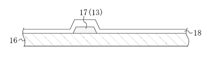
- FIG. 6 is a cross-sectional view schematically showing a glass substrate on which a gate line and a gate insulating film are formed.
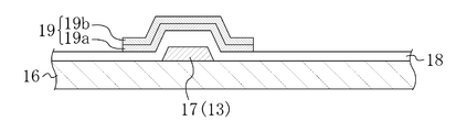
- FIG. 7 is a cross-sectional view schematically showing a glass substrate on which a semiconductor layer is formed.
- FIG. 1 is a plan view schematically showing the liquid crystal display device according to the first embodiment.
- FIG. 2 is a sectional view schematically showing a section taken along line II-II in FIG.
- FIG. 3 is a plan view schematically showing an
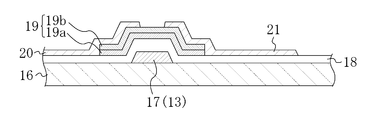
- FIG. 8 is a cross-sectional view schematically showing a glass substrate on which a source electrode and a drain electrode are formed.
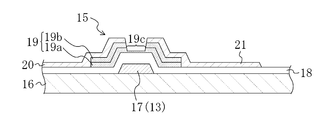
- FIG. 9 is a cross-sectional view schematically showing a glass substrate in which a channel portion is formed in a semiconductor layer.
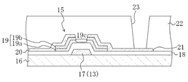
- FIG. 10 is a cross-sectional view schematically showing a glass substrate in a state where contact holes are formed in the laminated insulating film.
- FIG. 11 is a plan view schematically showing an enlarged part of a conventional active matrix substrate.
- FIG. 12 is a plan view schematically showing an enlarged part of a conventional active matrix substrate when pixel electrodes are formed in a shifted manner.
- Embodiment 1 of the Invention 1 to 10 show Embodiment 1 of the present invention.
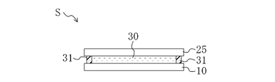
- FIG. 1 is a plan view schematically showing the liquid crystal display device S.
- FIG. 2 is a cross-sectional view schematically showing the liquid crystal display device S along the line II-II in FIG. 3 and 5 are enlarged views of a part of the pair of substrates 10 and 25 constituting the liquid crystal display device S, respectively.
- FIG. 4 is a cross-sectional view schematically showing the thin film transistor 15 along the line IV-IV in FIG.
- the liquid crystal display device S includes an active matrix substrate 10, a counter substrate 25 disposed to face the active matrix substrate 10, and a space between the active matrix substrate 10 and the counter substrate 25.
- the liquid crystal layer 30 is provided.
- the liquid crystal display device S includes a display unit D that includes a plurality of pixels (not shown) provided in a delta arrangement and displays an image.
- the active matrix substrate 10 and the counter substrate 25 are formed in, for example, a rectangular shape and the like, and although not shown, an alignment film is provided on the surface on the liquid crystal layer 30 side, and the surface on the opposite side to the liquid crystal layer 30 Are each provided with a polarizing plate. Between the active matrix substrate 10 and the counter substrate 25, a frame-shaped sealing material 31 made of an epoxy resin or the like is disposed, and a liquid crystal material is sealed inside the sealing material 31, whereby the above-mentioned A liquid crystal layer 30 is configured.
- the active matrix substrate 10 has, as a mounting region, a protruding portion 10 a that protrudes outward from the counter substrate 25 on one side and is exposed to the outside from the counter substrate 25.
- the projection 10a is supplied with an active circuit substrate 10 and a counter substrate 25 from an external circuit, such as an integrated circuit chip for driving a liquid crystal, and a signal for supplying power to the integrated circuit chip and displaying an image. And a flexible printed wiring board to be supplied to the circuit board.
- the active matrix substrate 10 includes a plurality of pixel electrodes 11 provided in a delta shape on the display unit D and a plurality of pixel electrodes 11 provided so as to extend in parallel with each other between the pixel electrodes 11.
- Gate lines 13 a plurality of source lines 14 provided between the pixel electrodes 11 so as to extend in parallel to each other in a direction orthogonal to the gate lines 13, and a plurality of thin film transistors respectively connected to the pixel electrodes 11.
- TFT Thin Film Transistor, hereinafter referred to as TFT
- Each pixel electrode 11 provided in a delta shape defines a plurality of rows 12 aligned in parallel to each other, and is provided with a half-pitch shift in the row direction (lateral direction in the figure) in each adjacent row 12a, 12b. It has been.
- Each pixel electrode 11 is formed in a rectangular shape, for example.
- the active matrix substrate 10 has a non-inversion structure in which the position of the TFT 15 is the same with respect to each pixel electrode 11.
- each pixel electrode 11 is formed in a rectangular shape.
- each pixel electrode 11 has various shapes such as a shape in which a rectangular electrode is partially cut out or a shape in which the electrode is partially protruded. It is possible to form in the shape.
- Each gate line 13 is linearly provided between the pixel electrodes 11 so as to extend in the row direction. Further, auxiliary capacitance lines (not shown) are provided between the gate lines 13 so as to extend along the gate lines 13 and overlap the drain electrodes 21 of the TFTs 15 described later in the respective rows.
- Each source line 14 is provided between the pixel electrodes 11 so as to extend in parallel with each other in a direction intersecting with each gate line 13 while being bent alternately left and right in the drawing, in other words, meandering in a crank shape.
- Each source line 14 is connected to each of the plurality of first linear portions 14a provided so as to extend along the left side of each pixel electrode 11 in the figure, and to each of the first linear portions 14a.
- the electrode 11 has a plurality of second linear portions 14b provided so as to extend to the middle portion of the sides along the sides on the upper and lower sides in the drawing.
- Each source line 14 is provided by alternately connecting the first linear portions 14a and the second linear portions 14b.
- each source line 14 includes a plurality of projecting portions 14c provided so as to extend from one end on the right side in the drawing in each second linear portion 14b along the sides on the upper and lower sides in the drawing of each pixel electrode 11. 14d. These protrusions 14c and 14d are formed with the same length.
- Each source line 14 is connected to each pixel electrode 11 disposed on the right side of the source line 14 in the drawing via a TFT 15.
- Each TFT 15 is alternately connected to each second linear portion 14 b and each projecting portion 14 c along each source line 14.
- Each TFT 15 is provided near the intersection of each gate line 13 and each source line 14 from the viewpoint of increasing the aperture ratio of each pixel. As shown in FIG. 4, each of these TFTs 15 is a bottom gate type TFT, and the semiconductor layer 19 of each TFT 15 is formed on a gate insulating film 18 provided so as to cover each gate line 13 and each auxiliary capacitance line. Is formed. Each source line 14 is also formed on the gate insulating film 18.
- Each semiconductor layer 19 is formed in an island shape on the gate insulating film 18 so as to straddle part of each gate line 13.
- a part of each gate line 13 that overlaps each semiconductor layer 19 via the gate insulating film 18 constitutes a gate electrode 17 of each TFT 15.
- Each semiconductor layer 19 is formed by stacking, for example, an intrinsic amorphous silicon layer 19a and an n + amorphous silicon layer 19b.
- the n + amorphous silicon layer 19b is divided into two parts by partially removing the region overlapping the gate electrode 17, and the region of the intrinsic amorphous silicon layer 19a exposed from the n + amorphous silicon layer 19b constitutes the channel portion 19c.
- a source electrode 20 connected to the source line 14 is formed on one n + amorphous silicon layer 19b and the gate insulating film 18.
- a drain electrode 21 connected to the pixel electrode 11 is formed on the other n + amorphous silicon layer 19 b and the gate insulating film 18.
- each TFT 15 is a bottom-gate TFT, but each TFT 15 may be a top-gate TFT.
- Each TFT 15 has a laminated insulating film 22 in which a silicon nitride film and an acrylic resin film (both not shown) are laminated in order.
- Each pixel electrode 11 is formed on the surface of the laminated insulating film 22.
- a plurality of contact holes 23 exposing a part of the drain electrode 21 in each TFT 15 to the bottom are formed in the laminated insulating film 22, and each drain electrode 21 is connected to each pixel electrode 11 through each contact hole 23. Has been.
- the counter substrate 25 is provided with a plurality of color filters 26 in the display portion D so as to overlap the pixel electrodes 11.
- the plurality of color filters 26 are constituted by, for example, three color filters such as a red color filter 26r, a green color filter 26g, and a blue color filter 26b, and define a plurality of rows 27 in the same manner as the pixel electrodes 11 described above. is doing.
- red, green, and blue color filters 26r, 26g, and 26b are periodically arranged in a line in the row direction. These color filters 26 are arranged so that the color filters 26 of the same color are arranged with a 1.5 pitch shift in the row direction for each row.
- a black matrix 28 is formed on the counter substrate 25 so as to partition each color filter 26, and a common electrode (not shown) is formed so as to cover each color filter 26 and the black matrix 28. .
- the liquid crystal display device S sequentially turns on the TFTs 15 connected to the gate lines 13 according to a predetermined gate signal input from the external circuit, and supplies a predetermined source signal to each source line 14.
- a predetermined gate signal input from the external circuit
- the liquid crystal display device S sequentially turns on the TFTs 15 connected to the gate lines 13 according to a predetermined gate signal input from the external circuit, and supplies a predetermined source signal to each source line 14.
- the liquid crystal molecules The desired display is performed by controlling the orientation of the.
- the active matrix substrate 10 and the counter substrate 25 are respectively manufactured, and both the substrates 10 and 25 are bonded to each other via the seal material 31, and the active matrix substrate 10 and the counter substrate 25 are bonded by the seal material 31.
- the integrated circuit chip and the flexible printed wiring board are mounted on the active matrix substrate 10, and the polarizing plates are attached to both the substrates 10 and 25. Since the liquid crystal display device S according to the present invention is particularly characterized by the active matrix substrate 10, a method for manufacturing the active matrix substrate 10 will be described in detail below with reference to FIGS. 6 to 10 are views for explaining a method of manufacturing the active matrix substrate 10, and are sectional views schematically showing an enlarged region of the glass substrate 16 on which the TFT 15 is formed.
- a metal film containing aluminum for example, a thickness of about 50 nm to 500 nm
- a metal film containing aluminum for example, a thickness of about 50 nm to 500 nm
- Patterning is performed by photolithography to form each gate line (each gate electrode 17) 13 and each auxiliary capacitance line as shown in FIG.
- a silicon nitride film (eg, a thickness of about 100 nm to 500 nm) or the like is formed on the entire surface on which each gate line (each gate electrode 17) 13 and each auxiliary capacitance line is formed by plasma CVD (Chemical Vapor Deposition) method.
- plasma CVD Chemical Vapor Deposition
- an intrinsic amorphous silicon film for example, a thickness of about 50 nm to 100 nm
- an n + amorphous silicon film for example, a thickness
- an n-type impurity element such as phosphorus
- each semiconductor layer 19 may be formed from an amorphous silicon film as described above, but may also be formed from a polysilicon film. Further, laser annealing treatment may be performed on the amorphous silicon film or the polysilicon film to improve crystallinity.
- a metal film containing, for example, aluminum (for example, a thickness of about 50 nm to 500 nm) is formed on the entire surface of the gate insulating film 18 on which each semiconductor layer 19 is formed by sputtering, and then the metal film is formed by photolithography.
- each source electrode 20 and each drain electrode 21 are formed and each source line 14 is formed as shown in FIG.
- each protrusion 14c, 14d is also formed with each 1st linear part 14a and each 2nd linear part 14b.
- each TFT 15 is formed.
- an acrylic resin film for example, a thickness of about 1000 nm to 5000 nm or the like is formed by a spin coating method. Is deposited to form a laminated insulating film 22.
- each contact hole 23 As shown in FIG.
- a transparent conductive film (for example, about 100 nm to 200 nm in thickness) made of ITO (Indium Tin Oxide) or the like is formed on the entire surface of the laminated insulating film 22 in which each contact hole 23 is formed by sputtering, and then the transparent Each pixel electrode 11 is formed by patterning the conductive film by photolithography.
- a polyimide resin is applied by a printing method so as to cover each pixel electrode 11, and then a rubbing process is performed to form an alignment film.
- the active matrix substrate 10 having a non-inverted structure is manufactured.
- the plurality of first lines are provided so as to extend while being alternately bent between the plurality of pixel electrodes 11 provided in the delta arrangement, and extend along the side of each pixel electrode 11.
- a plurality of source lines 14 having a plurality of second linear portions 14b that are connected to the first portions 14a and the first linear portions 14a and extend to the middle portion of the side along the side of each pixel electrode 11. Since each of the source lines 14 has a plurality of protrusions 14c and 14d extending from one end of each second linear portion 14b along the side of each pixel electrode 11, as shown in FIG.
- Differences in the lengths of the portions 14e, 14f, 14g, and 14h along the pixel electrodes 11 can be reduced on both sides of the pixel electrodes 11 in the direction in which the rows 12 are arranged. As a result, even if the formation positions of the respective pixel electrodes 11 and the respective source lines 14 are shifted, the difference in parasitic capacitance between the respective pixel electrodes 11 and the source lines 14 is suppressed in the adjacent rows 12a and 12b. it can. And it can suppress that a horizontal stripe pattern and roughness arise in an image display, and can improve display quality.
- each protrusion part 14c, 14d is formed in the mutually same length, in each source line 14, the part 14e, 14f along these pixel electrodes 11 on both sides of the direction where each row 12 in each pixel electrode 11 is located in a line. , 14g and 14h can be eliminated. As a result, in the adjacent rows 12a and 12b, the difference in parasitic capacitance between each pixel electrode 11 and the source line 14 can be suppressed as much as possible.
- the protrusions 14c and 14d have the same length, but the present invention is not limited to this, and the protrusions 14c and 14d have different lengths. May be. As described above, even if the lengths of the projecting portions 14c and 14d are different from each other, the portions 14e and 14f along the pixel electrodes 11 on both sides of the source electrodes 14 in the row direction of the rows 12 of the pixel electrodes 11 , 14g, and 14h can be reduced, and a difference in parasitic capacitance between each pixel electrode 11 and the source line 14 can be suppressed in adjacent rows 12a and 12b.
- each TFT 15 is alternately connected to each second linear portion 14b and each projecting portion 14c.
- each TFT 15 includes each first linear portion. 14a and each protrusion 14c may be alternately connected.
- the liquid crystal display device S having the active matrix substrate 10 has been described.
- the present invention is not limited to this, and may be applied to other display devices having an active matrix substrate such as an organic electroluminescence display device. Is possible.
- the gate lines 13 are provided so as to extend linearly between the pixel electrodes 11, and the source lines 14 are provided so as to extend while alternately bending between the pixel electrodes 11.
- each source line is provided so as to extend linearly between each pixel electrode, and each gate line is alternately bent between each pixel electrode so as to extend in a direction intersecting each source line. It may be provided. That is, each gate line extends along the side of each pixel electrode, and a plurality of first linear portions are connected to each of the first linear portions along the side of each pixel electrode.
- a plurality of second linear portions provided so as to extend to an intermediate portion of the side edges, and a plurality of protrusions provided so as to extend along one side of each pixel electrode from one end of each second linear portion. May have a part.
- the present invention is useful for an active matrix substrate and a liquid crystal display device.
- each pixel electrode and source line It is suitable for an active matrix substrate and a liquid crystal display device that are required to suppress the difference in parasitic capacitance between them.
Landscapes
- Physics & Mathematics (AREA)
- Nonlinear Science (AREA)
- Engineering & Computer Science (AREA)
- Microelectronics & Electronic Packaging (AREA)
- Mathematical Physics (AREA)
- Chemical & Material Sciences (AREA)
- Crystallography & Structural Chemistry (AREA)
- General Physics & Mathematics (AREA)
- Optics & Photonics (AREA)
- Liquid Crystal (AREA)
Abstract
Description
次に、本発明の作用について説明する。
(10) アクティブマトリクス基板
(11) 画素電極
(13) ゲート線
(14) ソース線
(14a) 第1線状部
(14b) 第2線状部
(14c,14d) 突出部
(15) TFT(薄膜トランジスタ)
(25) 対向基板
(30) 液晶層
(31) シール材
図1~図10は、本発明の実施形態1を示している。図1は、液晶表示装置Sを概略的に示す平面図である。図2は、図1のII-II線に沿って液晶表示装置Sを概略的に示す断面図である。図3及び図5は、液晶表示装置Sを構成する一対の基板10,25の一部をそれぞれ拡大して示す図である。図4は、図3のIV-IV線に沿って薄膜トランジスタ15を概略的に示す断面図である。
次に、上記アクティブマトリクス基板10の作製方法及び上記液晶表示装置Sの製造方法について説明する。
したがって、この実施形態1によると、デルタ配列に設けられた複数の画素電極11の間で交互に屈曲しながら延びるように設けられ、各画素電極11の側辺に沿って延びる複数の第1線状部14a、及び各第1線状部14aに連結して各画素電極11の側辺に沿ってその側辺の中間部分まで延びる複数の第2線状部14bを有する複数のソース線14が、各第2線状部14bの一方端から各画素電極11の側辺に沿って延びる複数の突出部14c,14dを有しているため、図3に示すように、各ソース線14において、各画素電極11における各行12の並ぶ方向の両側でそれら各画素電極11に沿う部分14e,14f,14g,14hの長さの差を小さくできる。これによって、各画素電極11と各ソース線14との形成位置がずれたとしても、隣り合う行12a,12bにおいて、互いの各画素電極11とソース線14との間の寄生容量の差を抑制できる。そして、画像表示に横縞模様やざらつきが生じることを抑制でき、表示品位を向上させることができる。
上記実施形態1では、各突出部14c,14dの互いの長さが同じになっているとしたが、本発明はこれに限られず、各突出部14c,14dは、互いの長さが異なっていてもよい。このように各突出部14c,14dの互いの長さが異なっていても、各ソース線14において、各画素電極11における各行12の並ぶ方向の両側でそれら各画素電極11に沿う部分14e,14f,14g,14hの長さの差を小さくでき、隣り合う行12a,12bにおいて、互いの各画素電極11とソース線14との間の寄生容量の差を抑制することが可能になる。
Claims (3)
- デルタ配列に設けられた複数の画素電極と、
上記各画素電極の間に互いに平行に延びるように線状に設けられた複数のゲート線と、
上記各画素電極の間に交互に屈曲しながら上記各ゲート線と交差する方向に互いに平行に延びるように設けられた複数のソース線と、
上記各画素電極にそれぞれ接続された複数の薄膜トランジスタとを備え、
上記各ソース線は、上記各画素電極の側辺に沿って延びるように設けられた複数の第1線状部、該各第1線状部に連結して上記各画素電極の側辺に沿って該側辺の中間部分まで延びるように設けられた複数の第2線状部、及び該各第2線状部の一方端から上記各画素電極の側辺に沿って延びるように設けられた複数の突出部を有し、
上記各薄膜トランジスタは、上記各ソース線に沿って、上記各第1線状部又は上記各第2線状部と上記各突出部とに交互に接続されている
ことを特徴とするアクティブマトリクス基板。 - 請求項1に記載のアクティブマトリクス基板において、
上記各突出部は、互いに同じ長さで形成されている
ことを特徴とするアクティブマトリクス基板。 - 請求項1に記載のアクティブマトリクス基板と、
上記アクティブマトリクス基板に対向して配置された対向基板と、
上記アクティブマトリクス基板と上記対向基板との間に設けられた液晶層とを有する
ことを特徴とする液晶表示装置。
Priority Applications (5)
| Application Number | Priority Date | Filing Date | Title |
|---|---|---|---|
| EP08870159.4A EP2230657B1 (en) | 2008-01-10 | 2008-09-08 | Active matrix substrate and liquid crystal display device |
| JP2009548806A JP5149910B2 (ja) | 2008-01-10 | 2008-09-08 | アクティブマトリクス基板及び液晶表示装置 |
| US12/744,654 US8274464B2 (en) | 2008-01-10 | 2008-09-08 | Active matrix substrate and liquid crystal display device |
| BRPI0819192 BRPI0819192A2 (pt) | 2008-01-10 | 2008-09-08 | Substrato de matriz ativa e dispositivo de exibição de cristal líquido. |
| CN2008801103898A CN101821791B (zh) | 2008-01-10 | 2008-09-08 | 有源矩阵基板及液晶显示装置 |
Applications Claiming Priority (2)
| Application Number | Priority Date | Filing Date | Title |
|---|---|---|---|
| JP2008003236 | 2008-01-10 | ||
| JP2008-003236 | 2008-01-10 |
Publications (1)
| Publication Number | Publication Date |
|---|---|
| WO2009087705A1 true WO2009087705A1 (ja) | 2009-07-16 |
Family
ID=40852831
Family Applications (1)
| Application Number | Title | Priority Date | Filing Date |
|---|---|---|---|
| PCT/JP2008/002470 Ceased WO2009087705A1 (ja) | 2008-01-10 | 2008-09-08 | アクティブマトリクス基板及び液晶表示装置 |
Country Status (7)
| Country | Link |
|---|---|
| US (1) | US8274464B2 (ja) |
| EP (1) | EP2230657B1 (ja) |
| JP (1) | JP5149910B2 (ja) |
| CN (1) | CN101821791B (ja) |
| BR (1) | BRPI0819192A2 (ja) |
| RU (1) | RU2444068C2 (ja) |
| WO (1) | WO2009087705A1 (ja) |
Families Citing this family (11)
| Publication number | Priority date | Publication date | Assignee | Title |
|---|---|---|---|---|
| JP5551553B2 (ja) * | 2010-09-29 | 2014-07-16 | 株式会社ジャパンディスプレイ | 液晶表示装置 |
| US9024918B2 (en) * | 2012-08-16 | 2015-05-05 | Eastman Kodak Company | Display apparatus with pixel-aligned electrode |
| US9134860B2 (en) * | 2012-08-16 | 2015-09-15 | Eastman Kodak Company | Method of making a display device |
| JP2014095897A (ja) * | 2012-10-12 | 2014-05-22 | Semiconductor Energy Lab Co Ltd | 液晶表示装置 |
| JP2015014635A (ja) * | 2013-07-03 | 2015-01-22 | 株式会社ジャパンディスプレイ | 液晶表示装置 |
| JPWO2015166857A1 (ja) * | 2014-04-28 | 2017-04-20 | シャープ株式会社 | アクティブマトリクス基板、及びそれを備えた表示装置 |
| KR102403204B1 (ko) * | 2014-12-23 | 2022-05-30 | 삼성디스플레이 주식회사 | 표시장치 |
| CN104597675A (zh) * | 2015-02-06 | 2015-05-06 | 京东方科技集团股份有限公司 | 显示基板及显示装置 |
| JP6597097B2 (ja) * | 2015-09-15 | 2019-10-30 | 凸版印刷株式会社 | 薄膜トランジスタアレイ |
| CN114756147B (zh) * | 2017-02-15 | 2025-12-30 | 夏普株式会社 | 带位置输入功能的显示装置 |
| JP7345293B2 (ja) * | 2019-06-28 | 2023-09-15 | スタンレー電気株式会社 | 液晶素子、照明装置 |
Citations (10)
| Publication number | Priority date | Publication date | Assignee | Title |
|---|---|---|---|---|
| JPH03212621A (ja) * | 1990-01-18 | 1991-09-18 | Toshiba Corp | 液晶表示装置 |
| JPH04184323A (ja) * | 1990-11-19 | 1992-07-01 | Sanyo Electric Co Ltd | 液晶表示装置 |
| JPH0580353A (ja) * | 1991-09-20 | 1993-04-02 | Toshiba Corp | 液晶表示装置 |
| JPH1090718A (ja) * | 1996-09-18 | 1998-04-10 | Sharp Corp | 液晶表示装置 |
| JPH11119254A (ja) | 1997-10-17 | 1999-04-30 | Sharp Corp | 反射型液晶表示装置 |
| WO2000020918A1 (en) * | 1998-10-07 | 2000-04-13 | Seiko Epson Corporation | Liquid crystal device and electronic apparatus |
| JP2000194017A (ja) * | 1998-12-28 | 2000-07-14 | Seiko Epson Corp | 液晶表示装置および電子機器 |
| JP2001051286A (ja) * | 1999-08-05 | 2001-02-23 | Seiko Epson Corp | 液晶表示装置の配線パターン、液晶表示装置および電子機器 |
| JP2001154223A (ja) * | 1999-11-29 | 2001-06-08 | Casio Comput Co Ltd | 液晶表示素子 |
| JP2002151699A (ja) * | 2000-11-15 | 2002-05-24 | Casio Comput Co Ltd | アクティブマトリクス型液晶表示装置 |
Family Cites Families (4)
| Publication number | Priority date | Publication date | Assignee | Title |
|---|---|---|---|---|
| US7227603B1 (en) * | 1993-07-22 | 2007-06-05 | Semiconductor Energy Laboratory Co., Ltd. | Liquid-crystal electro-optical apparatus and method of manufacturing the same |
| JPH08240811A (ja) | 1996-03-11 | 1996-09-17 | Casio Comput Co Ltd | 薄膜トランジスタパネル |
| US6221444B1 (en) | 1998-06-10 | 2001-04-24 | Canon Kabushiki Kaisha | Liquid crystal device |
| JP4276965B2 (ja) * | 2004-02-04 | 2009-06-10 | シャープ株式会社 | 表示装置 |
-
2008
- 2008-09-08 EP EP08870159.4A patent/EP2230657B1/en not_active Not-in-force
- 2008-09-08 US US12/744,654 patent/US8274464B2/en not_active Expired - Fee Related
- 2008-09-08 WO PCT/JP2008/002470 patent/WO2009087705A1/ja not_active Ceased
- 2008-09-08 RU RU2010117363/12A patent/RU2444068C2/ru not_active IP Right Cessation
- 2008-09-08 BR BRPI0819192 patent/BRPI0819192A2/pt not_active IP Right Cessation
- 2008-09-08 JP JP2009548806A patent/JP5149910B2/ja not_active Expired - Fee Related
- 2008-09-08 CN CN2008801103898A patent/CN101821791B/zh not_active Expired - Fee Related
Patent Citations (10)
| Publication number | Priority date | Publication date | Assignee | Title |
|---|---|---|---|---|
| JPH03212621A (ja) * | 1990-01-18 | 1991-09-18 | Toshiba Corp | 液晶表示装置 |
| JPH04184323A (ja) * | 1990-11-19 | 1992-07-01 | Sanyo Electric Co Ltd | 液晶表示装置 |
| JPH0580353A (ja) * | 1991-09-20 | 1993-04-02 | Toshiba Corp | 液晶表示装置 |
| JPH1090718A (ja) * | 1996-09-18 | 1998-04-10 | Sharp Corp | 液晶表示装置 |
| JPH11119254A (ja) | 1997-10-17 | 1999-04-30 | Sharp Corp | 反射型液晶表示装置 |
| WO2000020918A1 (en) * | 1998-10-07 | 2000-04-13 | Seiko Epson Corporation | Liquid crystal device and electronic apparatus |
| JP2000194017A (ja) * | 1998-12-28 | 2000-07-14 | Seiko Epson Corp | 液晶表示装置および電子機器 |
| JP2001051286A (ja) * | 1999-08-05 | 2001-02-23 | Seiko Epson Corp | 液晶表示装置の配線パターン、液晶表示装置および電子機器 |
| JP2001154223A (ja) * | 1999-11-29 | 2001-06-08 | Casio Comput Co Ltd | 液晶表示素子 |
| JP2002151699A (ja) * | 2000-11-15 | 2002-05-24 | Casio Comput Co Ltd | アクティブマトリクス型液晶表示装置 |
Non-Patent Citations (1)
| Title |
|---|
| See also references of EP2230657A4 * |
Also Published As
| Publication number | Publication date |
|---|---|
| US20100245223A1 (en) | 2010-09-30 |
| US8274464B2 (en) | 2012-09-25 |
| EP2230657A1 (en) | 2010-09-22 |
| RU2444068C2 (ru) | 2012-02-27 |
| BRPI0819192A2 (pt) | 2015-05-05 |
| CN101821791A (zh) | 2010-09-01 |
| JPWO2009087705A1 (ja) | 2011-05-19 |
| EP2230657B1 (en) | 2014-03-26 |
| CN101821791B (zh) | 2012-11-21 |
| JP5149910B2 (ja) | 2013-02-20 |
| RU2010117363A (ru) | 2011-11-10 |
| EP2230657A4 (en) | 2011-07-20 |
Similar Documents
| Publication | Publication Date | Title |
|---|---|---|
| JP5149910B2 (ja) | アクティブマトリクス基板及び液晶表示装置 | |
| EP2784574B1 (en) | Tft array substrate and forming method thereof, and display panel | |
| US8330893B2 (en) | Active matrix substrate and display device equipped with the same | |
| CN104133331B (zh) | 用于窄边框型液晶显示装置的阵列基板及其制造方法 | |
| US11435636B2 (en) | Method of manufacturing liquid crystal display device using first and second photoresists | |
| US8274618B2 (en) | Pixel structure and pixel array | |
| EP2518558B1 (en) | Liquid crystal display and array substrate | |
| US8502945B2 (en) | Array substrate of fringe field switching mode liquid crystal display panel and method of manufacturing the same | |
| US9535300B2 (en) | Pixel structure and liquid crystal panel | |
| US9298054B2 (en) | Liquid crystal display device and method of manufacturing the same | |
| JP2006317516A (ja) | 液晶表示装置及びその製造方法 | |
| JP4881475B2 (ja) | アクティブマトリクス基板及び液晶表示装置 | |
| US20150138475A1 (en) | Array substrate and liquid crystal display panel provided with same | |
| JP2010074030A (ja) | 薄膜トランジスタおよび電気光学装置 | |
| US8421941B2 (en) | TFT substrate and method of manufacturing the same | |
| WO2014080825A1 (ja) | 半導体装置、及び表示装置 | |
| US20070132902A1 (en) | Lcd and method of manufacturing the same | |
| KR20140006281A (ko) | 표시 장치 | |
| US7329901B2 (en) | Thin-film semiconductor device, electro-optical device, and electronic apparatus | |
| JP7739277B2 (ja) | ディスプレイパネル及びディスプレイ装置 | |
| KR102193377B1 (ko) | 액정 디스플레이 장치 | |
| JP2007305641A (ja) | アクティブマトリクス基板および液晶表示パネル | |
| KR20130034247A (ko) | 평판 표시장치용 박막 트랜지스터 기판 및 그 제조 방법 |
Legal Events
| Date | Code | Title | Description |
|---|---|---|---|
| WWE | Wipo information: entry into national phase |
Ref document number: 200880110389.8 Country of ref document: CN |
|
| 121 | Ep: the epo has been informed by wipo that ep was designated in this application |
Ref document number: 08870159 Country of ref document: EP Kind code of ref document: A1 |
|
| WWE | Wipo information: entry into national phase |
Ref document number: 2009548806 Country of ref document: JP |
|
| WWE | Wipo information: entry into national phase |
Ref document number: 2010117363 Country of ref document: RU |
|
| WWE | Wipo information: entry into national phase |
Ref document number: 2872/CHENP/2010 Country of ref document: IN |
|
| WWE | Wipo information: entry into national phase |
Ref document number: 2008870159 Country of ref document: EP |
|
| WWE | Wipo information: entry into national phase |
Ref document number: 12744654 Country of ref document: US |
|
| NENP | Non-entry into the national phase |
Ref country code: DE |
|
| ENP | Entry into the national phase |
Ref document number: PI0819192 Country of ref document: BR Kind code of ref document: A2 Effective date: 20100505 |