WO2009087874A1 - Appareil et procédé de test, carte-sonde - Google Patents
Appareil et procédé de test, carte-sonde Download PDFInfo
- Publication number
- WO2009087874A1 WO2009087874A1 PCT/JP2008/072967 JP2008072967W WO2009087874A1 WO 2009087874 A1 WO2009087874 A1 WO 2009087874A1 JP 2008072967 W JP2008072967 W JP 2008072967W WO 2009087874 A1 WO2009087874 A1 WO 2009087874A1
- Authority
- WO
- WIPO (PCT)
- Prior art keywords
- test
- signal
- device under
- drivers
- under test
- Prior art date
- Legal status (The legal status is an assumption and is not a legal conclusion. Google has not performed a legal analysis and makes no representation as to the accuracy of the status listed.)
- Ceased
Links
Images




Classifications
-
- G—PHYSICS
- G01—MEASURING; TESTING
- G01R—MEASURING ELECTRIC VARIABLES; MEASURING MAGNETIC VARIABLES
- G01R31/00—Arrangements for testing electric properties; Arrangements for locating electric faults; Arrangements for electrical testing characterised by what is being tested not provided for elsewhere
- G01R31/28—Testing of electronic circuits, e.g. by signal tracer
- G01R31/317—Testing of digital circuits
- G01R31/3181—Functional testing
- G01R31/319—Tester hardware, i.e. output processing circuits
- G01R31/31917—Stimuli generation or application of test patterns to the device under test [DUT]
- G01R31/31928—Formatter
Definitions
- the present invention relates to a test apparatus, a probe card, and a test method.
- This application is related to the following US applications and claims priority from the following US applications: For designated countries where incorporation by reference of documents is permitted, the contents described in the following application are incorporated into this application by reference and made a part of this application.
- a test apparatus for testing a device under test such as a semiconductor circuit
- an apparatus provided with a plurality of driver comparator pins that exchange signals with the device under test is known.
- a binary test signal can be generated from each driver comparator pin and supplied to the device under test.
- the binary test signal may be a signal having a logic pattern including binary logic values of H logic and L logic, for example.
- FIG. 8 is a diagram illustrating an example of a test apparatus 400 that generates a multi-value test signal.
- the test apparatus 400 includes a pin electronics unit 410 and a probe card 420.
- the pin electronics unit 410 includes a plurality of drivers 412 and a plurality of comparators 414. Each driver 412 outputs a binary test signal.
- the probe card 420 has a plurality of transmission paths 422 and needles 424.
- the plurality of transmission paths 422 are provided in one-to-one correspondence with the plurality of drivers 412.
- Each transmission path 422 transmits a test signal output from the corresponding driver 412.
- the tip of each transmission path 422 is short-circuited in the probe card 420.
- One end of the needle 424 is fixed to each short-circuited transmission path 422 by solder or the like. Further, the other end of the needle 424 contacts a terminal of the device under test and supplies a test signal received via the transmission path 422 to the device under test.
- the plurality of drivers 412 synchronously output the test signals, so that the plurality of test signals are synthesized in the probe card 420, and the multi-value test signals can be supplied to the device under test.
- each driver 412 generates a binary test signal of H logic (1 V) and L logic (0 V).
- the logical value (signal level) of the combined signal is the logical value (0 V) when both drivers 412 output L logic, one driver 412 outputs H logic, and the other driver 412 outputs L logic.
- a multi-value test signal can be generated using a binary driver comparator pin mounted on a conventional test apparatus.
- each driver 412 outputs a test signal at the same time, if the delay amount of each transmission path 422 is different, a multi-value test signal cannot be synthesized accurately.
- TDR Time Domain Reflectometry
- the TDR method is a method for measuring the delay time of a transmission line by inputting a signal to the transmission line with the open end and measuring the delay time of the signal reflected at the front end of the transmission line.
- the comparator 414 since the comparator 414 is connected to the transmission line 422 that is common to the driver 412, the delay of the transmission line 422 is determined from the timing at which the signal is output from the driver 412 and the timing at which the comparator 414 detects the reflected wave. Time can be measured easily.
- the description regarding a prior art document is abbreviate
- the tip of the transmission line 422 is short-circuited and fixed by solder or the like, so that the delay of the transmission line 422 by the TDR method.
- the time cannot be measured. That is, since no reflected wave is generated at the tip of each transmission line 422, the delay time of the transmission line 422 cannot be measured by the TDR method.
- first transmission path 422-1 and the second transmission path 422- 2 are calculated based on the timing at which a signal is output from the first driver 412-1 and the timing at which the second comparator 414-2 detects the signal.
- the sum of delay times in 2 can be measured.
- the delay times of the first transmission path 422-1 and the second transmission path 422-2 cannot be measured, it is difficult to adjust the timing at which each driver 412 outputs a signal. For this reason, it has been difficult to accurately generate a multi-value test signal.
- an object of one aspect of the present invention is to provide a test apparatus, a probe card, and a test method that can solve the above-described problems. This object is achieved by a combination of features described in the independent claims.
- the dependent claims define further advantageous specific examples of the present invention.
- a test apparatus for testing a device under test, wherein a plurality of test signals are synthesized by supplying a test signal output from each to the same terminal of the device under test.
- a plurality of drivers for supplying a multi-value signal to the terminal, and a plurality of drivers are provided in one-to-one correspondence with each of the drivers, and when testing the device under test, each tip is connected to the same terminal in the device under test.
- a plurality of probe pins that are electrically connected to each other so that a signal output from a corresponding driver is supplied to the corresponding terminal of the device under test, and when the device under test is not tested, each tip is electrically open;
- a test apparatus is provided.
- a test apparatus for testing a device under test, a plurality of drivers each outputting a test signal, a pin electronics unit in which a plurality of drivers are formed, and a pin electronics unit A wiring unit that electrically connects the output terminals of a plurality of drivers on the board and generates a multi-value signal in which a plurality of test signals are synthesized, and a multi-value that the wiring unit transmits outside the pin electronics unit And a probe pin that supplies the signal to the device under test.
- a probe card for use in a test apparatus including a plurality of drivers each outputting a test signal, provided in one-to-one correspondence with a plurality of drivers, When testing, when each tip is electrically connected to the same terminal of the device under test, the signal output by the corresponding driver is supplied to the terminal of the device under test, and the device under test is not tested
- a probe card is provided that includes a plurality of probe pins in which the respective tip portions are electrically opened.
- a device under test is used using a test apparatus that includes a plurality of drivers each outputting a test signal and a plurality of probe pins that supply a test signal output from the corresponding driver to the device under test.
- This is a test method for testing a device.
- the tip of each probe pin is opened, the adjustment signal is output to each driver, and the adjustment signal reflected at the tip of the probe pin is measured and measured.
- Based on the results adjust the timing at which each driver outputs the test signal, electrically connect the tip of each probe pin to the same terminal of the device under test, and output the test signal to each driver
- To supply a device under test with a multi-level signal that combines test signals output by multiple drivers. The law provides.
- FIG. 1 is a diagram illustrating a configuration example of a test apparatus 100 according to an embodiment.
- FIG. 2 is a view showing a probe card 50 together with a device under test 200. An example of the side view which looked at the probe card 50 and the device under test 200 from the position A in FIG. 2 is shown.
- 3 is a diagram illustrating a configuration example of a signal generation unit 12 and a signal processing unit 14.
- FIG. 2 is a flowchart illustrating an operation example of the test apparatus 100. It is a figure which shows the other example of the probe card. It is a figure which shows the other structural example of the pin electronics part 30 and the probe card. It is a figure which shows an example of the test apparatus 400 which produces
- FIG. 1 is a diagram illustrating a configuration example of a test apparatus 100 according to an embodiment.
- the test apparatus 100 tests a device under test such as a semiconductor circuit using a multi-value test signal.
- the test apparatus 100 includes a plurality of signal generation units 12, a plurality of signal processing units 14, a pin electronics unit 30, and a probe card 50.
- the pin electronics unit 30 includes a plurality of drivers 32, a plurality of comparators 34, and a plurality of resistors 36.
- the plurality of drivers 32 are provided in one-to-one correspondence with the plurality of signal generation units 12.
- Each signal generator 12 generates a test signal and supplies it to the corresponding driver 32.
- Each signal generation unit 12 may generate a binary test signal having a logic pattern including binary logic values of H logic and L logic, for example.
- the signal generation unit 12 may generate a voltage waveform that the test signal should have and supply it to the driver 32.
- the driver 32 outputs a voltage corresponding to the received voltage waveform.
- the driver 32 may output a current consumed by the device under test in accordance with the test signal.
- Each driver 32 supplies a test signal to the probe card 50 via the resistor 36.
- the plurality of drivers 32 supply test signals output from the respective terminals to the same terminal of the device under test, thereby supplying a multi-value signal obtained by synthesizing the plurality of test signals to the terminal.
- a plurality of transmission lines 52 and a plurality of probe pins 54 are fixed to the probe card 50.
- the plurality of transmission paths 52 are formed on the probe card 50 in one-to-one correspondence with the plurality of drivers 32.
- the plurality of probe pins 54 are provided in one-to-one correspondence with the plurality of transmission paths 52.
- Each transmission path 52 transmits the signal output from the corresponding driver 32 to the corresponding probe pin 54.
- Each probe pin 54 has a connection portion 56 and a tip portion 58.
- the connecting portion 56 and the tip portion 58 may be both ends of the probe pin 54.
- the connection portion 56 of each probe pin 54 is fixed on the substrate of the probe card 50 and connected to the transmission path 52.
- Each probe pin 54 is electrically connected to the same terminal in the device under test when testing the device under test.
- each probe pin 54 is formed such that the tip portion 58 protrudes from the surface of the probe card 50, and contacts the same terminal of the device under test arranged to face the probe card 50.
- a multi-value signal obtained by synthesizing a plurality of test signals output from the plurality of drivers 32 is supplied to the device under test.
- each probe pin 54 is formed so that each tip 58 is electrically opened when the device under test is not tested. In other words, each probe pin 54 is formed so that the tip 58 is normally open and is electrically connected via the pad of the device under test when testing the device under test.
- the signal output from the driver 32 when the device under test is not tested is reflected at the tip 58 of the probe pin 54.
- the signal reflected at the tip 58 of the probe pin 54 is measured by the corresponding comparator 34.
- the plurality of comparators 34 are provided in one-to-one correspondence with the plurality of drivers 32, and the input ends of the respective comparators 34 are electrically connected to the output ends of the corresponding drivers 32.
- Each comparator 34 measures a response signal output from the device under test when the device under test is tested.
- each comparator 34 measures the adjustment signal output from the driver 32 and the reflected wave thereof.
- Each comparator 34 in this example measures a signal transmitted through a connection point between the resistor 36 and the transmission path 52.
- the comparator 34 receives the adjustment signal output from the driver 32 via the resistor 36 and receives the reflected wave of the adjustment signal via the transmission line 52.
- the comparator 34 is provided in one-to-one correspondence with the driver 32 in one-to-one correspondence with the driver 32 in another example.
- one comparator 34 may be provided for the plurality of drivers 32.
- the comparators 34 are arranged so that the distance (signal transmission time) between the comparator 34 and each driver 32 is sufficiently small to be negligible with respect to the delay time in the transmission path 52.
- the comparator 34 may sequentially measure the adjustment signal output from the driver 32 and the reflected wave thereof for each driver 32.
- the signal processing unit 14 may calculate the delay time in the transmission path 52 based on the elapsed time from when the comparator 34 detects the adjustment signal until the reflected wave of the adjustment signal is detected. For example, the signal processing unit 14 may calculate 1 ⁇ 2 of the elapsed time as the delay time in the transmission path 52. The signal processing unit 14 adjusts the timing at which each driver 32 outputs a test signal based on the delay time in each transmission path 52.
- the device under test can be tested by generating a multi-value test signal of three or more values using the driver 32 that generates a binary signal. Further, the delay time in each transmission path 52 can be easily measured by the TDR method. For this reason, the output timing of the signal in each driver 32 can be easily adjusted, and a multi-value test signal can be generated with high accuracy.
- test apparatus 100 having two drivers 32, two transmission paths 52, and two probe pins 54 will be described. 100 may have a greater number of drivers 32, transmission lines 52, and probe pins 54. Further, the test apparatus 100 may have the same number of other components such as the comparators 34 corresponding thereto. The test apparatus 100 may generate a plurality of multi-value test signals in parallel using these, or may generate a multi-value test signal and a binary test signal in parallel.
- the resistor 36 matches the impedance between the transmission line 52 and the driver 32.
- the resistor 36 may have substantially the same impedance as the transmission line 52.
- the probe card 50 is provided so as to be replaceable with respect to the test apparatus 100.
- the user or the like applies the multi-value test signal of three or more values to the device under test, and the device under test using the binary test signal without using the multi-value test signal.
- the probe card 50 used when testing the above may be prepared in advance. The user or the like may replace the probe card 50 according to the type of test to be performed.
- FIG. 2 is a diagram showing the probe card 50 together with the device under test 200.
- the device under test 200 may be tested in a state where it is formed on a semiconductor wafer on a disk, for example.
- the device under test 200 has a terminal 210. Although one terminal 210 is shown in FIG. 2, the device under test 200 may have a plurality of terminals 210.
- the test apparatus 100 can apply a multi-value test signal to the terminal 210.
- FIG. 3 shows an example of a side view of the probe card 50 and the device under test 200 as seen from the position A in FIG.
- the device under test 200 of this example is arranged to face the probe card 50.
- Each probe pin 54 is formed so as to protrude in the direction of the device under test 200 from the surface of the probe card 50, and contacts a common terminal 210 in the device under test 200.
- the common terminal 210 may have a width that allows contact with the plurality of tip portions 58.
- the width of the common terminal 210 that contacts the plurality of probe pins 54 may be larger than the width of the terminal that contacts one probe pin 54.
- the plurality of probe pins 54 may be formed such that the interval between the tip portions 58 is smaller than the interval between the connection portions 56. Further, the interval between the tip portions 58 may be narrower than the width of the terminal 210 of the device under test 200.
- the intervals between the tip portions 58 of the plurality of probe pins 54 that generate the multi-value test signal may be narrower than the intervals between the tip portions 58 of the plurality of probe pins 54 that generate a plurality of binary test signals in parallel.
- the plurality of probe pins 54 may be arranged in a substantially straight line along an arrangement direction substantially parallel to the terminals of the device under test 200 provided in a substantially straight line. Further, when a plurality of terminals are provided on each side of the device under test 200, the plurality of probe pins 54 may be provided in two rows so as to face each row of terminals.
- the interval in the arrangement direction of the tip portions 58 of some probe pins 54 is the same as that of the tip portions 58 of other probe pins 54.
- a plurality of probe pins 54 may be formed so as to be different from the interval in the arrangement direction. That is, the plurality of probe pins 54 may be formed such that a plurality of types of intervals are mixed as the intervals in the arrangement direction of the tip portions 58 of the plurality of probe pins 54.
- FIG. 4 is a diagram illustrating a configuration example of the signal generation unit 12 and the signal processing unit 14.
- one signal generation unit 12 and one signal processing unit 14 are shown, but each signal generation unit 12 may have the same configuration, and each signal processing unit 14 also has the same configuration. You can do it.
- each signal generation unit 12 includes a pattern generation unit 16, a timing generation unit 20, and a waveform shaping unit 18.
- the pattern generator 16 generates a logical pattern that the test signal and the adjustment signal output from the signal generator 12 should have.
- the pattern generator 16 may generate a binary logic pattern.
- the timing generator 20 generates the timing information of the test signal and the adjustment signal output from the signal generator 12. For example, the timing generator 20 may generate a timing signal that determines the phase (or edge position), period (or bit rate), etc. of the signal.
- the waveform shaping unit 18 generates a test signal and an adjustment signal based on the logic pattern generated by the pattern generation unit 16 and the timing signal generated by the timing generation unit 20.
- the waveform shaping unit 18 may shape the voltage waveform of the signal.
- the waveform shaping unit 18 supplies the generated signal to the driver 32.
- the timing measurement unit 24 receives the signal measured by the comparator 34.
- the comparator 34 of this example outputs a comparison result signal indicating the magnitude relationship between the voltage level of the input signal and the applied reference level VOL as a binary logical value.
- the timing measurement unit 24 sequentially acquires the logical value of the comparison result signal at a timing corresponding to the given strobe signal pulse.
- the signal generator 12 When testing the device under test 200, the signal generator 12 outputs a test signal. For example, the signal generator 12 may output a test signal having a logic pattern determined by a user or the like.
- the comparator 34 receives a response signal output from the device under test 200 in response to the test signal, and the timing measurement unit 24 acquires a logical value pattern of the comparison result signal output from the comparator 34.
- the determination unit 26 determines pass / fail of the device under test 200 based on whether or not the logical value pattern acquired by the timing measurement unit 24 matches a predetermined expected value pattern.
- the signal generator 12 When measuring the delay time of the transmission path 52, the signal generator 12 outputs an adjustment signal. For example, the signal generation unit 12 may output a step signal or one pulse as the adjustment signal.
- the comparator 34 sequentially receives the adjustment signal output from the driver 32 and the reflected wave thereof. In the timing measurement unit 24, the comparator 34 sequentially receives the comparison result signal output for the adjustment signal and the comparison result signal output for the reflected wave, and sequentially acquires the respective logical value patterns.
- the pattern generator 16 and the timing generator 20 When measuring the delay time of the transmission path 52, the pattern generator 16 and the timing generator 20 output a predetermined logic pattern and timing signal so that the driver 32 outputs an adjustment signal.
- the synchronization adjustment unit 22 may instruct that the delay time of the transmission line 52 is measured.
- the synchronization adjustment unit 22 adjusts the timing at which the driver 32 outputs a signal based on the adjustment signal measured by the comparator 34 and the timing measurement unit 24 and the measurement result of the reflected wave. For example, the synchronization adjustment unit 22 may calculate a difference in timing when the comparator 34 detects a corresponding edge in the adjustment signal and the reflected wave based on the measurement result in the timing measurement unit 24. The timing difference corresponds to the delay time of the transmission path 52.
- Each synchronization adjustment unit 22 adjusts the timing at which the corresponding driver 32 outputs a signal based on the delay time of the corresponding transmission line 52. That is, each synchronization adjusting unit 22 is configured so that the test signals applied to the device under test 200 from the respective drivers 32 via the transmission path 52 are applied to the device under test 200 at substantially the same timing. The signal output timing of each driver 32 is adjusted according to the delay time of the transmission path 52.
- each synchronization adjusting unit 22 may adjust the signal output timing of each driver 32 based on the difference in delay time of each transmission path 52 with respect to a predetermined reference delay time. As the reference delay time, the delay time of any one of the transmission paths 52 may be used. In addition, the synchronization adjustment unit 22 may adjust the signal output timing of the driver 32 by adjusting the phase of the timing signal output from the timing generation unit 20.
- the signal output timing in each driver 32 can be adjusted to synthesize a multi-value test signal with high accuracy. For this reason, the device under test 200 can be tested with high accuracy.
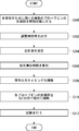
- FIG. 5 shows a flowchart for explaining an operation example of the test apparatus 100.
- the test apparatus 100 adjusts the signal output timing of each driver 32 before testing the device under test 200.
- the device under test 200 is not brought into contact with the probe pin 54, and the tip portions 58 of the plurality of probe pins 54 used for generating the multi-value signal are respectively opened (S300).
- an adjustment signal is output from each driver 32 (S302).
- each synchronization adjustment unit 22 may calculate the delay time of each transmission path 52 from the timing difference at which each comparator 34 detects the adjustment signal and the reflected wave.
- each synchronization adjustment unit 22 adjusts the signal output timing in each driver 32 based on the calculated delay time (S308).
- the device under test 200 After adjusting the driver 32, the device under test 200 is arranged at a position facing the probe card 50, and the tip portion 58 of each probe pin 54 that generates a multilevel signal is brought into contact with the same terminal of the device under test 200. (S310). Then, a test signal is output from each driver 32 to test the device under test 200 (S312). With such an operation, the device under test 200 can be tested by generating a multilevel signal with high accuracy.
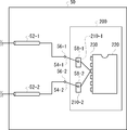
- FIG. 6 is a diagram illustrating another example of the probe card 50.
- the probe card 50 in this example includes a plurality of transmission paths 52 and a plurality of probe pins 54, similarly to the probe card 50 described with reference to FIGS.
- each probe pin 54 makes a one-to-one contact with each terminal 210 of the device under test 200.
- the terminal 210 may be an electrode formed on a semiconductor wafer.
- Each terminal 210 is connected to a common input pin 230 in the circuit section 220 of the device under test 200.
- FIG. 7 is a diagram illustrating another configuration example of the pin electronics unit 30 and the probe card 50.
- the pin electronics unit 30 of this example includes a plurality of drivers 32, a plurality of comparators 34, and a wiring unit 42.
- the plurality of drivers 32 and the plurality of comparators 34 may be the same as the driver 32 and the plurality of comparators 34 described with reference to FIGS.
- the wiring unit 42 electrically connects the output terminals of the plurality of drivers 32 on the substrate of the pin electronics unit 30 to generate a multi-value signal in which a plurality of test signals are synthesized.
- the wiring unit 42 includes a plurality of resistors 36, a common resistor 38, and a common transmission path 40.
- the plurality of resistors 36 may be the same as the plurality of resistors 36 described in connection with FIGS.
- the common resistor 38 is connected to a plurality of resistors 36.
- One end of the common transmission path 40 is electrically connected to the probe card 50, and the other end is electrically connected to the output end of each driver 32 via the common resistor 38.
- the common transmission path 40 may be provided so that signal delay times from the output ends of the respective drivers 32 to the common transmission path 40 are substantially equal. More specifically, the common transmission line 40 is preferably provided in the vicinity of each driver 32 so that the signal delay time from the output end of each driver 32 to the common transmission line 40 can be regarded as almost zero. .
- the common resistor 38 matches the impedance between the resistor 36 provided at the output of each driver 32 and the common transmission path 40.
- the impedance of the common resistor 38 may be half of the impedance of each resistor 36.
- the probe card 50 has a probe pin 54.
- the probe pin 54 may be the same as the probe pin 54 described in connection with FIGS.
- the probe pin 54 receives the multi-value test signal transmitted by the common transmission path 40 outside the substrate of the pin electronics unit 30 and supplies it to the device under test 200. Note that the probe pins 54 of this example are in one-to-one contact with the terminals 210 of the device under test 200.
- the test apparatus 100 of this example since the signal delay time from each driver 32 to the common transmission path 40 is substantially zero, if the test signals are simultaneously output from each driver 32, the multi-value test signal is accurately obtained. Can be generated well. Further, the common resistor 38 and the common transmission path 40 may be formed in the probe card 50.
- a device under test can be tested by generating a multi-value test signal of three or more values using a driver that generates a binary signal.
- the delay time in each transmission path can be easily measured by the TDR method. For this reason, the output timing of the signal in each driver can be easily adjusted, and a multi-value test signal can be generated with high accuracy.
Landscapes
- Engineering & Computer Science (AREA)
- General Engineering & Computer Science (AREA)
- Physics & Mathematics (AREA)
- General Physics & Mathematics (AREA)
- Tests Of Electronic Circuits (AREA)
Abstract
La présente invention concerne un appareil de test permettant de tester un dispositif à tester. L'appareil de test est muni d'une pluralité de programmes d'essai qui fournissent un signal à valeurs multiples, une pluralité de signaux de test y étant synthétisée, vers un même terminal du dispositif à tester, et ce en fournissant des signaux de test produits par les programmes d'essai respectifs au même terminal. L'appareil de test est également muni d'une pluralité de broches de sonde, agencées une à une pour les programmes d'essai et électriquement connectées au même terminal du dispositif à tester, sur chaque section d'extrémité conductrice, et qui fournissent les signaux produits par les programmes d'essai correspondants au terminal du dispositif à tester, et permet à chaque section d'extrémité conductrice de se trouver dans un état électriquement ouvert lorsque le dispositif n'est pas testé.
Priority Applications (1)
| Application Number | Priority Date | Filing Date | Title |
|---|---|---|---|
| JP2009548874A JPWO2009087874A1 (ja) | 2008-01-08 | 2008-12-17 | 試験装置、プローブカード、および試験方法 |
Applications Claiming Priority (2)
| Application Number | Priority Date | Filing Date | Title |
|---|---|---|---|
| US11/971,207 US7755375B2 (en) | 2008-01-08 | 2008-01-08 | Test apparatus, probe card, and test method |
| US11/971,207 | 2008-01-08 |
Publications (1)
| Publication Number | Publication Date |
|---|---|
| WO2009087874A1 true WO2009087874A1 (fr) | 2009-07-16 |
Family
ID=40844061
Family Applications (1)
| Application Number | Title | Priority Date | Filing Date |
|---|---|---|---|
| PCT/JP2008/072967 Ceased WO2009087874A1 (fr) | 2008-01-08 | 2008-12-17 | Appareil et procédé de test, carte-sonde |
Country Status (4)
| Country | Link |
|---|---|
| US (1) | US7755375B2 (fr) |
| JP (1) | JPWO2009087874A1 (fr) |
| TW (1) | TWI386667B (fr) |
| WO (1) | WO2009087874A1 (fr) |
Cited By (2)
| Publication number | Priority date | Publication date | Assignee | Title |
|---|---|---|---|---|
| JP2018066739A (ja) * | 2016-10-21 | 2018-04-26 | 新特系統股▲フン▼有限公司Sync−Tech System Corporation | プローブカードモジュール |
| JP2022515270A (ja) * | 2018-12-25 | 2022-02-17 | 中興通訊股▲ふん▼有限公司 | コネクタ構造、遅延時間差の計算方法および装置 |
Families Citing this family (4)
| Publication number | Priority date | Publication date | Assignee | Title |
|---|---|---|---|---|
| JP5429727B2 (ja) * | 2007-08-24 | 2014-02-26 | ワイアイケー株式会社 | 半導体試験装置 |
| US8988081B2 (en) * | 2011-11-01 | 2015-03-24 | Teradyne, Inc. | Determining propagation delay |
| JP6545213B2 (ja) * | 2017-03-17 | 2019-07-17 | アンリツ株式会社 | 3値信号発生装置及び3値信号発生方法 |
| US10564219B2 (en) | 2017-07-27 | 2020-02-18 | Teradyne, Inc. | Time-aligning communication channels |
Citations (6)
| Publication number | Priority date | Publication date | Assignee | Title |
|---|---|---|---|---|
| JPH025937U (fr) * | 1988-06-27 | 1990-01-16 | ||
| JPH04259868A (ja) * | 1991-02-14 | 1992-09-16 | Advantest Corp | Ic試験装置 |
| JPH09196970A (ja) * | 1996-01-24 | 1997-07-31 | Advantest Corp | プローブカード |
| JP2001153886A (ja) * | 1999-11-26 | 2001-06-08 | Mitsubishi Electric Corp | プローブカード、及びこれを備えたテスト装置 |
| JP2002257901A (ja) * | 2001-02-27 | 2002-09-11 | Ando Electric Co Ltd | スキュータイミング調整装置および方法 |
| JP2004117247A (ja) * | 2002-09-27 | 2004-04-15 | Advantest Corp | 半導体試験装置のプローバインタフェース装置及び半導体試験装置のデバイスインターフェース装置 |
Family Cites Families (11)
| Publication number | Priority date | Publication date | Assignee | Title |
|---|---|---|---|---|
| US4746855A (en) * | 1984-03-14 | 1988-05-24 | Teradyne, Inc. | Relay multiplexing for circuit testers |
| SE464909B (sv) | 1988-02-19 | 1991-07-01 | Tandlaekare Dyfvermark Ab | Dental bitkloss foer anslutning till sugkaella |
| JPH01287484A (ja) * | 1988-05-16 | 1989-11-20 | Hitachi Ltd | プローブヘッド及びその製造方法とそれを用いた半導体lsi検査装置 |
| JP2688941B2 (ja) * | 1988-08-29 | 1997-12-10 | 株式会社アドバンテスト | 位相補正装置 |
| JP2831780B2 (ja) * | 1990-02-02 | 1998-12-02 | 株式会社アドバンテスト | Ic試験装置 |
| US5371654A (en) * | 1992-10-19 | 1994-12-06 | International Business Machines Corporation | Three dimensional high performance interconnection package |
| US6246245B1 (en) * | 1998-02-23 | 2001-06-12 | Micron Technology, Inc. | Probe card, test method and test system for semiconductor wafers |
| US6448799B1 (en) * | 1999-09-30 | 2002-09-10 | Hitachi Electronics Engineering Co., Ltd. | Timing adjustment method and apparatus for semiconductor IC tester |
| US7064564B2 (en) * | 2001-02-01 | 2006-06-20 | Antares Contech, Inc. | Bundled probe apparatus for multiple terminal contacting |
| US20060214679A1 (en) * | 2005-03-28 | 2006-09-28 | Formfactor, Inc. | Active diagnostic interface for wafer probe applications |
| JP4911495B2 (ja) * | 2006-05-15 | 2012-04-04 | ルネサスエレクトロニクス株式会社 | 半導体集積回路用ソケット |
-
2008
- 2008-01-08 US US11/971,207 patent/US7755375B2/en active Active
- 2008-12-17 WO PCT/JP2008/072967 patent/WO2009087874A1/fr not_active Ceased
- 2008-12-17 JP JP2009548874A patent/JPWO2009087874A1/ja active Pending
-
2009
- 2009-01-07 TW TW098100362A patent/TWI386667B/zh active
Patent Citations (6)
| Publication number | Priority date | Publication date | Assignee | Title |
|---|---|---|---|---|
| JPH025937U (fr) * | 1988-06-27 | 1990-01-16 | ||
| JPH04259868A (ja) * | 1991-02-14 | 1992-09-16 | Advantest Corp | Ic試験装置 |
| JPH09196970A (ja) * | 1996-01-24 | 1997-07-31 | Advantest Corp | プローブカード |
| JP2001153886A (ja) * | 1999-11-26 | 2001-06-08 | Mitsubishi Electric Corp | プローブカード、及びこれを備えたテスト装置 |
| JP2002257901A (ja) * | 2001-02-27 | 2002-09-11 | Ando Electric Co Ltd | スキュータイミング調整装置および方法 |
| JP2004117247A (ja) * | 2002-09-27 | 2004-04-15 | Advantest Corp | 半導体試験装置のプローバインタフェース装置及び半導体試験装置のデバイスインターフェース装置 |
Cited By (6)
| Publication number | Priority date | Publication date | Assignee | Title |
|---|---|---|---|---|
| JP2018066739A (ja) * | 2016-10-21 | 2018-04-26 | 新特系統股▲フン▼有限公司Sync−Tech System Corporation | プローブカードモジュール |
| KR20180044222A (ko) * | 2016-10-21 | 2018-05-02 | 싱크-테크 시스템 코포레이션 | 프로브 카드 모듈 |
| KR102202461B1 (ko) * | 2016-10-21 | 2021-01-14 | 싱크-테크 시스템 코포레이션 | 프로브 카드 모듈 |
| JP2022515270A (ja) * | 2018-12-25 | 2022-02-17 | 中興通訊股▲ふん▼有限公司 | コネクタ構造、遅延時間差の計算方法および装置 |
| US11995389B2 (en) | 2018-12-25 | 2024-05-28 | Zte Corporation | Connector structure, and skew calculation method and device |
| JP7498176B2 (ja) | 2018-12-25 | 2024-06-11 | 中興通訊股▲ふん▼有限公司 | コネクタ試験治具、遅延時間差の計算方法および試験装置 |
Also Published As
| Publication number | Publication date |
|---|---|
| TW200933179A (en) | 2009-08-01 |
| US20090174420A1 (en) | 2009-07-09 |
| JPWO2009087874A1 (ja) | 2011-05-26 |
| US7755375B2 (en) | 2010-07-13 |
| TWI386667B (zh) | 2013-02-21 |
Similar Documents
| Publication | Publication Date | Title |
|---|---|---|
| JP5279724B2 (ja) | 試験装置およびキャリブレーション方法 | |
| CN101048780B (zh) | 用于校准和/或校直通信信道的方法和装置 | |
| KR100548199B1 (ko) | 아날로그/디지털 혼합 신호 반도체 디바이스 테스트 장치 | |
| WO2009087874A1 (fr) | Appareil et procédé de test, carte-sonde | |
| US6924651B2 (en) | Printed board inspecting apparatus | |
| KR101138296B1 (ko) | 시험 장치, 드라이버 컴퍼레이터 칩, 응답 측정 장치, 교정 방법 및 교정 장치 | |
| US6784684B2 (en) | Testing apparatus including testing board having wirings connected to common point and method of testing semiconductor device by composing signals | |
| US8892381B2 (en) | Test apparatus and manufacturing method | |
| CN101484819B (zh) | 自动测试装置及与其配套使用的校准设备和校准方法 | |
| KR100994811B1 (ko) | 시험 장치 및 퍼포먼스 보드 | |
| KR19990045518A (ko) | 파형 취득 동작 모드를 지니는 자동 회로 테스터 | |
| JP5475666B2 (ja) | スキュー測定方法および試験装置 | |
| KR100736680B1 (ko) | 반도체 소자 테스트 장치의 캘리브레이션 방법 | |
| KR20160059526A (ko) | 전자 장치의 테스트 장치 및 시스템 | |
| JP5066184B2 (ja) | 試験装置および伝送装置 | |
| CN111381104A (zh) | 一种传输通道阻抗的测量方法和装置 | |
| JP5038137B2 (ja) | 半導体試験装置 | |
| US7206985B2 (en) | Method and apparatus for calibrating a test system for an integrated semiconductor circuit | |
| JP4846134B2 (ja) | 試験装置、及びキャリブレーション方法 | |
| TWI401451B (zh) | Output device and test device | |
| JP2011053098A (ja) | プリント回路基板の検査システム及びプリント回路基板の検査方法 | |
| JP2002122634A (ja) | 半導体試験装置のタイミング確認方法及びタイミング補正方法及び補正装置 |
Legal Events
| Date | Code | Title | Description |
|---|---|---|---|
| 121 | Ep: the epo has been informed by wipo that ep was designated in this application |
Ref document number: 08869484 Country of ref document: EP Kind code of ref document: A1 |
|
| WWE | Wipo information: entry into national phase |
Ref document number: 2009548874 Country of ref document: JP |
|
| NENP | Non-entry into the national phase |
Ref country code: DE |
|
| 122 | Ep: pct application non-entry in european phase |
Ref document number: 08869484 Country of ref document: EP Kind code of ref document: A1 |