WO2009088071A1 - Elément semi-conducteur de réception de lumière et dispositif de communication optique - Google Patents
Elément semi-conducteur de réception de lumière et dispositif de communication optique Download PDFInfo
- Publication number
- WO2009088071A1 WO2009088071A1 PCT/JP2009/050203 JP2009050203W WO2009088071A1 WO 2009088071 A1 WO2009088071 A1 WO 2009088071A1 JP 2009050203 W JP2009050203 W JP 2009050203W WO 2009088071 A1 WO2009088071 A1 WO 2009088071A1
- Authority
- WO
- WIPO (PCT)
- Prior art keywords
- layer
- semiconductor light
- conductive
- receiving element
- light receiving
- Prior art date
- Legal status (The legal status is an assumption and is not a legal conclusion. Google has not performed a legal analysis and makes no representation as to the accuracy of the status listed.)
- Ceased
Links
Images





Classifications
-
- H—ELECTRICITY
- H10—SEMICONDUCTOR DEVICES; ELECTRIC SOLID-STATE DEVICES NOT OTHERWISE PROVIDED FOR
- H10F—INORGANIC SEMICONDUCTOR DEVICES SENSITIVE TO INFRARED RADIATION, LIGHT, ELECTROMAGNETIC RADIATION OF SHORTER WAVELENGTH OR CORPUSCULAR RADIATION
- H10F77/00—Constructional details of devices covered by this subclass
- H10F77/10—Semiconductor bodies
- H10F77/14—Shape of semiconductor bodies; Shapes, relative sizes or dispositions of semiconductor regions within semiconductor bodies
- H10F77/148—Shapes of potential barriers
-
- H—ELECTRICITY
- H10—SEMICONDUCTOR DEVICES; ELECTRIC SOLID-STATE DEVICES NOT OTHERWISE PROVIDED FOR
- H10F—INORGANIC SEMICONDUCTOR DEVICES SENSITIVE TO INFRARED RADIATION, LIGHT, ELECTROMAGNETIC RADIATION OF SHORTER WAVELENGTH OR CORPUSCULAR RADIATION
- H10F77/00—Constructional details of devices covered by this subclass
- H10F77/30—Coatings
- H10F77/306—Coatings for devices having potential barriers
- H10F77/331—Coatings for devices having potential barriers for filtering or shielding light, e.g. multicolour filters for photodetectors
- H10F77/337—Coatings for devices having potential barriers for filtering or shielding light, e.g. multicolour filters for photodetectors using interference filters, e.g. multilayer dielectric filters
-
- Y—GENERAL TAGGING OF NEW TECHNOLOGICAL DEVELOPMENTS; GENERAL TAGGING OF CROSS-SECTIONAL TECHNOLOGIES SPANNING OVER SEVERAL SECTIONS OF THE IPC; TECHNICAL SUBJECTS COVERED BY FORMER USPC CROSS-REFERENCE ART COLLECTIONS [XRACs] AND DIGESTS
- Y02—TECHNOLOGIES OR APPLICATIONS FOR MITIGATION OR ADAPTATION AGAINST CLIMATE CHANGE
- Y02E—REDUCTION OF GREENHOUSE GAS [GHG] EMISSIONS, RELATED TO ENERGY GENERATION, TRANSMISSION OR DISTRIBUTION
- Y02E10/00—Energy generation through renewable energy sources
- Y02E10/50—Photovoltaic [PV] energy
Definitions
- the present invention is based on the priority claim of Japanese Patent Application No. 2008-003182 (filed on Jan. 10, 2008), the entire contents of which are incorporated herein by reference. Shall.
- the present invention relates to a semiconductor light receiving element and an optical communication device including the semiconductor light receiving element, and more particularly, to a semiconductor light receiving element that converts an optical signal used in a communication field and an information processing field into an electric signal, and the semiconductor light receiving element.
- the present invention relates to an optical communication device.
- semiconductor light receiving elements are often used as photoelectric conversion elements.
- the main factors that limit the response speed of photoelectric conversion in semiconductor light-receiving elements are the circuit time constant determined by the product of the load resistance and the capacitance created by the depletion layer, and the carrier transit time required for carriers to pass through the depletion layer. In order to improve the high-speed response of the semiconductor light receiving element, it is required to reduce the circuit time constant and the carrier transit time.
- the Schottky photodiode using surface plasmon described in Patent Document 2 is excited by a hole having a diameter smaller than the wavelength of incident light and incident light on a film surface of a conductive film provided around the hole. And a semiconductor layer provided in contact with the conductive film in the vicinity of the hole of the conductive film.
- the light incident on the periodic structure excites the surface plasmon, generates a resonance state with the surface plasmon, generates near-field light at the interface between the conductive film and the semiconductor layer, and is photoelectrically converted.
- the surface plasmon enhanced photovoltaic device described in Patent Document 3 has a surface illuminated by incident light and an unilluminated surface, and at least one of the illuminated surface and the unilluminated surface is incident A first having apertures having a diameter less than or equal to the wavelength of the light, wherein the apertures have periodic surface topography, and have an array of apertures having enhanced properties that cause resonant interaction between incident light and surface plasmons on the surface A metal electrode, a second electrode spaced from the first metal electrode, and a plurality of spheres disposed between the first metal electrode and the second electrode corresponding to the arrangement of the apertures, And each sphere has a first portion of p-doped material and a second portion of n-doped material such that a pn junction is formed at the junction between the first and second portions.
- Each sphere has a part Arranged in the aperture such that one of the first or second part is in electrical contact with the first metal electrode and the other of the first or second part is in electrical contact with the second electrode Has been.
- Incident light resonates with surface plasmons on the surface topography.
- the light receiving element described in Patent Document 4 is disposed above the semiconductor substrate, the n-type semiconductor layer disposed above the semiconductor substrate, and the n-type contact layer.
- JP 2007-165359 A International Publication No. 2005/098966 Pamphlet Japanese Patent No. 3726887 JP 2005-159002 A
- Patent Documents 1 to 4 are incorporated herein by reference. The following analysis is given from the perspective of the present invention.
- An object of the present invention is to provide a semiconductor light receiving element having a large light receiving area, high speed, and high efficiency, and an optical communication device including the semiconductor light receiving element.
- a substrate a first conductive type semiconductor layer formed on the substrate, a non-doped semiconductor light absorbing layer formed on the first conductive type semiconductor layer, and a non-doped type
- a semiconductor learning element including a second conductive type semiconductor layer formed on a semiconductor light absorption layer and a conductive layer formed on the second conductive type semiconductor layer.
- a plurality of openings arranged periodically are formed in the stacked body including the conductive layer, the second conductive type semiconductor layer, and the non-doped type semiconductor light absorption layer. The width of the opening is less than or equal to the wavelength of the incident light. The opening penetrates the conductive layer and the second conductive type semiconductor layer and reaches the non-doped type semiconductor light absorption layer.
- the plurality of openings have a periodic arrangement that causes surface plasmon resonance at the interface between the conductive layer and the second conductive type semiconductor layer.
- the opening depth is d
- the thickness of the conductive layer is t 1
- the thickness of the second conductive semiconductor layer is t 2
- the thickness of the non-doped semiconductor light absorption layer is when the t 3
- the depth d of the opening satisfies the condition of t 1 + t 2 ⁇ d ⁇ t 1 + t 2 + t 3/2.
- the semiconductor light receiving element further includes a first electrode formed on the first conductivity type semiconductor and electrically connected to the first conductivity type semiconductor layer.
- the conductive layer is electrically connected to the second conductivity type semiconductor layer and also functions as a second electrode.
- the semiconductor light receiving element is formed on the first conductive type semiconductor, and is electrically connected to the first conductive type semiconductor layer, and the second conductive type.
- a second electrode formed on the type semiconductor and electrically connected to the second conductivity type semiconductor layer.
- the conductive layer is formed on the second conductive type semiconductor layer via an insulating layer in a region where the second electrode is not formed, and the conductive layer and the second electrode are not electrically connected.
- At least a part of the substrate surface opposite to the surface on which the first conductivity type semiconductor layer is formed is formed in a lens shape.
- the plurality of openings are periodically arranged in a triangular lattice shape or a square lattice shape, and the surface shape of the openings is a circle, an ellipse, or a polygon.
- the ratio of the total area of the plurality of openings to the area of the upper surface of the conductive layer (including the area of the openings) is 50% or more and 80% or less.
- the refractive index of the second conductive semiconductor layer is n
- the period of the opening, which is the distance between the centers of adjacent openings is P
- ⁇ satisfies the condition of either 0.9 ⁇ nP / ⁇ ⁇ 1.1 or 1.2 ⁇ nP / ⁇ ⁇ 1.5.
- the semiconductor light receiving element further includes a Bragg reflective multilayer film below the first conductivity type semiconductor layer.
- the conductive layer includes at least one metal material of Al, Ag, Au, and Cu.
- the non-doped semiconductor light absorption layer includes Si, Si x Ge 1-x (where x is a positive number less than 1), Ge, GaN, GaAs, GaInAs, GaInP, and It is formed of at least one selected from the group of InP.
- the semiconductor light receiving element further includes an antireflection film or a protective film on the conductor layer.
- an optical communication device including a semiconductor light receiving element.
- a semiconductor light receiving element includes a substrate, a first conductive semiconductor layer formed on the substrate, a non-doped semiconductor light absorbing layer formed on the first conductive semiconductor layer, and a non-doped semiconductor light absorbing layer. And a second conductive type semiconductor layer formed on the second conductive type semiconductor layer and a conductive layer formed on the second conductive type semiconductor layer.
- a plurality of openings arranged periodically are formed in the stacked body including the conductive layer, the second conductive type semiconductor layer, and the non-doped type semiconductor light absorption layer. The width of the opening is less than or equal to the wavelength of the incident light. The opening penetrates the conductive layer and the second conductive type semiconductor layer and reaches the non-doped type semiconductor light absorption layer.
- the semiconductor light receiving element is arranged so that light enters from the substrate side.
- the present invention has at least one of the following effects.
- a conductive layer or second electrode having a periodic opening excites surface plasmons at the interface between the conductive layer and the semiconductor to form a resonance state.
- a strong electric field is generated in the non-doped semiconductor light absorption layer, and the thin non-doped semiconductor light absorption layer is efficiently absorbed.
- the element capacitance per unit area can be reduced.
- the light receiving area can be maintained even if the element capacity is reduced, alignment with an optical fiber or the like can be facilitated. Therefore, according to the present invention, a semiconductor light receiving element and an optical communication device with high efficiency, high speed, and high applicability are realized.
- a high-speed and high-efficiency semiconductor light-receiving element can be realized using Ge that is compatible with the Si CMOS process, so that high integration and mass production are easy, and the manufacturing cost can be reduced.
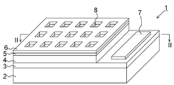
- FIG. 1 is a schematic perspective view of a semiconductor light receiving element according to a first embodiment of the present invention.
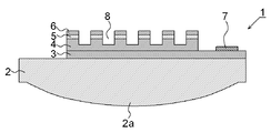
- FIG. 2 is a schematic sectional view taken along line II-II in FIG. 1.
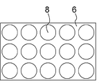
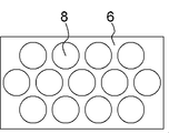
- the schematic plan view which shows another form of opening. 1 is a schematic cross-sectional view showing an aspect according to a first embodiment of the present invention.
- FIG. 3 is a schematic partial cross-sectional view of FIG. 2.
- the schematic sectional drawing of the semiconductor light receiving element concerning 2nd Embodiment of this invention.
- FIG. 6 is a schematic cross-sectional view of an optical communication device according to a fourth embodiment.
- FIG. 10 is a schematic cross-sectional view of an optical communication device according to a fifth embodiment.
- 2 is a schematic cross-sectional view of a semiconductor light receiving element according to a comparative example in Example 1.
- FIG. 1 is a schematic perspective view of the semiconductor light receiving element according to the first embodiment of the present invention.
- FIG. 2 is a schematic sectional view taken along line II-II in FIG.
- the semiconductor light-receiving element 1 of the present invention includes a substrate 2, a first conductive semiconductor layer 3, a non-doped semiconductor light absorption layer 4, and a second conductive semiconductor layer 5 in order from the lower layer, and the first conductive semiconductor layer. 3, the non-doped semiconductor light absorption layer 4 and the second conductive semiconductor layer 5 form a pin (or nip) semiconductor multilayer structure. Further, the semiconductor light receiving element 1 is formed on the second conductive semiconductor layer 5, the second electrode (conductive layer) 6 electrically connected to the second conductive semiconductor layer 5, and the first conductive semiconductor layer 3. The first electrode 7 is electrically connected to the first conductivity type semiconductor layer 3.
- the second electrode 6 is formed on the second conductive semiconductor layer 5 and also serves as a conductive layer that induces surface plasmon resonance.
- a reverse bias voltage is applied to the first electrode 7 and the second electrode 6, the non-doped semiconductor light absorption layer 4 is depleted, and photocarriers generated in the non-doped semiconductor light absorption layer 4 are taken out to an external circuit as a photocurrent. And converted into an electrical signal.
- the semiconductor light receiving element 1 has a plurality of openings 8 that penetrate the second electrode 6 and the second conductive semiconductor layer 5 and reach the non-doped semiconductor light absorption layer 4.
- the openings 8 are arranged periodically.
- the shape of the openings 8 in the planar projection of the second electrode 6 surface is a square, and the openings 8 are periodically arranged in a square lattice pattern.
- FIGS. 3 and 4 are schematic plan views showing other forms of the opening 8.
- the planar shape of the opening 8 may be a polygon other than a square, for example, a circle or an ellipse as shown in FIG.
- the openings 8 may be arranged in a triangular lattice shape as shown in FIG. 4, for example.
- each aperture 8 in the planar projection is set to be equal to or smaller than the incident wavelength.
- the portion that is the size of the opening 8 is preferably the widest (longest) portion of the opening.
- a square opening is a diagonal line
- a circular opening is a diameter.
- the ratio of the total area occupied by the openings 8 in the plane of the second electrode 6 is preferably increased with respect to the area of the second electrode 6. For example, when the ratio of the total area occupied by the openings 8 to the area of the second electrode (including the openings 8) is 50% or more, a remarkable effect of reducing the element capacitance can be obtained.
- a decrease in quantum efficiency due to an increase in the area ratio of the opening 8 can be prevented by utilizing the effect of surface plasmon resonance by the second electrode 6, but the upper limit of the area ratio of the opening 8 is desired. It is preferable to set appropriately according to the quantum efficiency and the device capacity, for example, 80% or less.
- the opening 8 can be formed by a general processing method such as wet etching or dry etching.
- the second electrode 6 having an opening pattern is formed on the semiconductor multilayer structures 3, 4, and 5 using a lift-off process, and the second conductive semiconductor layer 5 and the non-doped semiconductor are formed using the formed second electrode 6 as a mask.
- An opening can also be formed in the light absorption layer 4.
- the incident direction of light with respect to the semiconductor light receiving element 1 may be incident from the second electrode 6 surface side or incident from the substrate 2 surface side, and in either case, the same effect of surface plasmon resonance Can be obtained.
- incident light hardly passes through the aperture 8 having a size equal to or smaller than the wavelength, and the second electrode 6 also serves as a mirror, so that higher efficiency is obtained.
- the semiconductor layers 3 to 5 as shown in FIG.
- a convex portion 2a (lens shape) may be formed on the surface of the substrate 2 opposite to the substrate 2 so that the substrate 2 itself has a lens function.
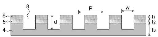
- FIG. 6 is a schematic partial cross-sectional view of the non-doped semiconductor light absorption layer 4, the second conductive semiconductor layer 5, and the second electrode 6 portion of the semiconductor light receiving element 1 shown in FIG.
- the distance between the centers of adjacent openings 8 is a period P
- the wavelength of incident light in a vacuum is ⁇
- the refractive index of the second conductivity type semiconductor layer 5 is n
- nP / ⁇ is 0.9. It is preferable that the condition of ⁇ nP / ⁇ ⁇ 1.1 or 1.2 ⁇ nP / ⁇ ⁇ 1.5 is satisfied. When nP / ⁇ is within this range, high quantum efficiency can be obtained.
- the opening depth d (depth of the opening 8 reaching from the second electrode 6 to the non-doped semiconductor light absorption layer 4) is an important parameter for the quantum efficiency and high-frequency characteristics in the semiconductor light-receiving element 1 of the present invention. . Since the electric field is small in the portion of the opening 8, the traveling time of the carrier generated in this portion becomes long, and the high-speed response is hindered. Therefore, in order to obtain a high-speed response, it is advantageous to form the opening 8 also in the non-doped semiconductor light absorption layer 4. However, in that case, the quantum efficiency is slightly lowered. Therefore, in order to achieve both efficiency and high speed, the depth of the opening 8 is preferably shallower than the middle of the non-doped semiconductor light absorption layer 4.
- the depth of the opening 8 is d
- the thickness of the second electrode 6 is t 1
- the thickness of the second conductive semiconductor layer 5 is t 2
- the thickness of the non-doped semiconductor light absorption layer 4 is t 3 .
- the material of the second electrode 6 is preferably a conductive metal.
- a metal such as Al or Cu, which is widely used in semiconductor devices and has established many processing techniques, can be used.
- a metal such as Au or Ag having a low electric resistance and a small surface plasmon loss is particularly preferable.
- a metal layer such as Ti, Ta, Cr, W, Ni, and Pt can be provided as an adhesion layer or a barrier layer.
- the film thickness of these adhesion layers or barrier layers is preferably 20 nm or less so as to reduce optical loss.
- an antireflection film or a protective film made of an insulator may be provided on the surface of the second electrode 6 (may be formed on the inner surface of the opening 8).
- SiO 2 , SiON, SiN, etc. which can be easily formed and can provide a stable film, are preferable.
- the second conductive semiconductor layer 5, the non-doped semiconductor light absorption layer 4, and the first conductive semiconductor layer 3 may be configured as a laminated structure of a plurality of semiconductor materials. You can choose the most suitable material.
- the non-doped semiconductor light absorption layer 4 is selected from the group consisting of Si, Si x Ge 1-x (where x is a positive number less than 1), Ge, GaN, GaAs, GaInAs, GaInP, and InP. At least one semiconductor material can be selected.
- InP when used as the material of the substrate 2, InP can be used for the first conductive semiconductor layer 3, InGaAs can be used for the non-doped semiconductor light absorption layer 4, and InAlAs can be used for the second conductive semiconductor layer 5.
- Si when Si is used as the material of the substrate 2, Si is used for the first conductive semiconductor layer 3 and the second conductive semiconductor layer 5, and Si x Ge 1-x or Ge is used for the non-doped semiconductor light absorption layer 4. Can be used.
- a combination of the first conductivity type and the second conductivity type is a pin type in which the first conductivity type semiconductor layer 3 is an n-type semiconductor and the second conductivity type semiconductor layer 5 is a p-type semiconductor.
- the structure may be a nip type structure in which the first conductive semiconductor layer 3 is a p-type semiconductor and the second conductive semiconductor layer 5 is an n-type semiconductor.
- an InP substrate 2 as a substrate an n-type InP layer 3 as a first conductive semiconductor layer, an i-type InGaAs layer 4 as a non-doped semiconductor light absorption layer, and a p-type InAlAs layer 5 as a second conductive semiconductor layer are stacked.
- These semiconductor layers 3, 4 and 5 can all be grown using molecular beam epitaxy or metal organic vapor phase epitaxy.
- a Ti / Pt / Au-p electrode 6 is formed as a second electrode.
- a Ti / Pt / Au—n electrode 7 is formed as a first electrode on the exposed surface.
- a good ohmic junction is formed between the electrodes 7 and 6 and the semiconductor layers 3 and 5.
- the Ti / Pt / Au-p electrode 6 the p-type InAlAs layer 5 and the i-type InGaAs layer 4, a plurality of openings 8 arranged periodically are formed. The opening 8 penetrates the Ti / Pt / Au-p electrode 6 and the p-type InAlAs layer 5 and reaches the middle of the i-type InGaAs layer 4.
- the i-type InGaAs layer 4 When a reverse bias voltage is applied to the semiconductor light receiving element 1, the i-type InGaAs layer 4 is depleted.
- the incident light wavelength is 1.3 ⁇ m or 1.55 ⁇ m used for optical communication, for example, the i-type InGaAs layer 4 has a sufficiently large absorption coefficient, and a highly efficient semiconductor light receiving element can be realized.
- InP is a transparent material that does not absorb the wavelength, and light can be incident from the InP substrate 2 side.
- FIG. 7 is a schematic cross-sectional view of a second example of the semiconductor element according to the first embodiment of the present invention.
- the semiconductor light receiving element 11 is based on the first embodiment of the present invention, but the semiconductor material is different from that of the semiconductor light receiving element according to the first example.
- an n-type Si layer 3 is formed as a second conductivity type semiconductor layer, a SiGe buffer layer 13 is formed thereon, and a non-doped semiconductor light is formed thereon.
- An i-type Ge layer 4 is provided as an absorption layer, a SiGe buffer layer 14 is formed thereon, and a p-type Si layer 5 is formed thereon as a second conductivity type semiconductor layer.
- the SiGe buffer layers 13 and 14 are provided on the n-type Si layer 3 and the i-type Ge layer 4, the i-type Ge layer 4 and the p-type Si layer 5 with few crystal defects can be epitaxially grown.
- a Cr / Ag-p electrode 6 is formed as a second electrode
- a Cr / Ag-n electrode 7 is formed as a first electrode.
- the semiconductor light-receiving element 11 of the present invention operates with respect to incident light of 1.3 ⁇ m or 1.55 ⁇ m, and Si absorbs in this wavelength band. There will be no transparent material.
- the i-type Ge layer 17 as the optical non-doped semiconductor absorption layer, there is an advantage that compatibility with the Si process is improved.
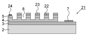
- FIG. 8 is a schematic sectional view of a semiconductor light receiving element according to the second embodiment of the present invention.
- the second electrode 6 has a structure also serving as a conductive layer having a periodic structure that induces surface plasmon resonance (the second electrode and the conductive layer are combined).
- the second electrode 24 and the conductive layer 23 having a periodic structure that induces surface plasmon resonance are configured separately.
- the second electrode 24 is formed on a part of the second conductive type semiconductor layer 5, and the conductive layer 23 is formed by forming the insulating layer 22 on the second conductive type semiconductor layer 5 on which the second electrode 24 is not formed. Is formed through. That is, the second electrode 24 and the conductive layer 23 are not electrically connected.
- a material of the insulating layer 22 for example, SiO 2 , SiON, SiN or the like is preferable.
- the thickness of the insulating layer 22 is appropriately set according to process suitability, incident light wavelength, and other various design parameters, but is preferably about 10 nm to 100 nm, and more preferably about 50 nm.
- the opening 8 passes through the conductive layer 23, the insulating layer 22, and the second conductive type semiconductor layer 5, and reaches the middle of the non-doped type semiconductor light absorption layer 4. Also in the configuration according to the second embodiment, the same surface plasmon resonance effect as in the first embodiment can be obtained.
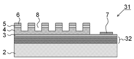
- FIG. 9 is a schematic cross-sectional view of a semiconductor light receiving element according to the third embodiment of the present invention.
- the difference from the first embodiment is that a Bragg reflective multilayer film 32 is provided between the substrate 2 and the first conductivity type semiconductor layer 3 in the third embodiment.
- the semiconductor light receiving element 31 is the same as the semiconductor light receiving element 1 according to the first embodiment shown in FIGS. 1 and 2.
- the semiconductor light-receiving element of the present invention light can be confined in the non-doped semiconductor light absorption layer using surface plasmon resonance, but there are still components that are transmitted or reflected.
- a Fabry-Perot resonator is formed between the second electrode 6 and the Bragg reflection multilayer film 32, and the quantum efficiency can be further increased (for example, 90% or more quantum efficiency is possible).
- the third embodiment has been described based on the first embodiment in which the second electrode 6 also serves as a conductive layer having a periodic structure.
- the second electrode is different from the conductive layer.
- the present invention can also be applied to the second embodiment.
- FIG. 10 is a schematic cross-sectional view of the optical communication device according to the fourth embodiment.
- the optical communication device 41 is an optical reception module, and can be an optical reception module for 40 Gbps transmission, for example.
- the optical communication device 41 includes a semiconductor light receiving element 42 of the present invention, an electrical wiring 43, a preamplifier IC 44, a chip carrier 45, a lens 46, and an optical fiber 47 in a module housing 48.
- the semiconductor light receiving element 41 is mounted on a chip carrier 45 and optically coupled by an optical fiber 47 and a lens 46.
- the semiconductor light receiving element 41 is electrically connected to the subsequent preamplifier IC 44 by the electric wiring 43.
- the semiconductor light receiving element 41 of the present invention is arranged so that light is irradiated from the substrate side, it can efficiently perform photoelectric conversion. It is also possible to arrange so that light is irradiated from the second electrode or the conductive layer side.
- the semiconductor light-receiving element 41 according to the present invention can be a compound semiconductor substrate or a substrate obtained by epitaxially growing Ge on Si.
- the use of the semiconductor light receiving element 41 according to the present invention has an advantage that the light receiving area can be increased and the coupling tolerance can be increased.
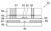
- FIG. 11 is a schematic cross-sectional view of an optical communication device (particularly, an LSI chip interconnect) according to the fifth embodiment.
- the optical communication device 51 includes an LSI package 54 as a semiconductor device, a semiconductor light receiving element / light source mounting board 55 mounted with the semiconductor light receiving element 52 and the VCSEL light source of the present invention, an LSI mounted with a concave mirror 63 and optical signal fibers 61 and 62. And a mounting board 56.
- the optical signal from the optical signal input fiber 62 is irradiated to the semiconductor light receiving element 52 by the concave mirror 63.
- the semiconductor light receiving element 52 corresponds to the optical signal to the LSI package 54 via the semiconductor light receiving element electric wiring layer 60 and the semiconductor light receiving element electric wiring via 58 electrically connected to the semiconductor light receiving element electric wiring layer 60.
- Apply current
- other generally known means such as a planar optical waveguide can be used instead of the optical signal input fiber 62 for inputting the optical signal.
- a condensing mechanism such as a convex lens can be used instead of the concave mirror 63.
- a preamplifier for amplifying electrical signals can be placed on the electrical wiring layer 60 for semiconductor light receiving elements.
- the electric signal from the LSI package 54 is converted into an optical signal by a VCSEL (surface emitting laser) light source 53 having an electric modulation mechanism through a light source / modulation electric wiring via 57 and a light source / modulation electric wiring layer 59.
- the optical signal is reflected by the concave mirror 63 and sent to the optical signal output fiber 61.
- the VCSEL light source 53 having an electric modulation mechanism is replaced with another known mechanism that modulates light by electricity, for example, a Mach-Zehnder type modulator that modulates light from an external light source by an electro-optic effect or a thermo-optic effect. Can do.
- light irradiation to the semiconductor light receiving element can be performed from the substrate side and from the second electrode or the conductive layer side, but photoelectric conversion can be performed more efficiently by irradiation from the substrate side. .
- the simulation model of the semiconductor light receiving element according to the present invention is a model according to the first embodiment as shown in FIGS. 2 and 6, in which the wavelength ⁇ of the incident light in vacuum is 1550 nm, and the thickness of the non-doped semiconductor light absorption layer.
- the aperture is made as thin as 250 nm, the shape of the opening is square, the width (length) w of one side of the opening is half of the period P, and the ratio of the total area of the opening to the area of the second electrode (including the opening) is 25 As a percentage, the simulation was performed with the setting where light was incident from the substrate side.
- the second electrode (not shown) does not exist in the light receiving part, and is provided at a location slightly away from the light receiving part.
- the setting in the comparative example is also light incidence from the substrate side.
- FIG. 13 shows the result of the electromagnetic field simulation.
- the refractive index of the second conductivity type semiconductor layer is n
- the horizontal axis is a value obtained by normalizing the period P by ⁇ / n
- the vertical axis is the quantum efficiency.
- the quantum efficiency is remarkable when the condition of 0.9 ⁇ nP / ⁇ ⁇ 1.1 or 1.2 ⁇ nP / ⁇ ⁇ 1.5 is satisfied. It can be seen that the quantum efficiency is about three times that of the comparative example. Moreover, higher efficiency than the comparative example is obtained also in parts other than the resonance peak. This is because when the light is incident from the substrate side, the light hardly transmits through an opening having a wavelength smaller than the wavelength, so that the second electrode also plays a role as a mirror.
Landscapes
- Light Receiving Elements (AREA)
Abstract
Priority Applications (2)
| Application Number | Priority Date | Filing Date | Title |
|---|---|---|---|
| JP2009548966A JP5170110B2 (ja) | 2008-01-10 | 2009-01-09 | 半導体受光素子及び光通信デバイス |
| US12/811,863 US8637951B2 (en) | 2008-01-10 | 2009-01-09 | Semiconductor light receiving element and optical communication device |
Applications Claiming Priority (2)
| Application Number | Priority Date | Filing Date | Title |
|---|---|---|---|
| JP2008003182 | 2008-01-10 | ||
| JP2008-003182 | 2008-01-10 |
Publications (1)
| Publication Number | Publication Date |
|---|---|
| WO2009088071A1 true WO2009088071A1 (fr) | 2009-07-16 |
Family
ID=40853180
Family Applications (1)
| Application Number | Title | Priority Date | Filing Date |
|---|---|---|---|
| PCT/JP2009/050203 Ceased WO2009088071A1 (fr) | 2008-01-10 | 2009-01-09 | Elément semi-conducteur de réception de lumière et dispositif de communication optique |
Country Status (3)
| Country | Link |
|---|---|
| US (1) | US8637951B2 (fr) |
| JP (1) | JP5170110B2 (fr) |
| WO (1) | WO2009088071A1 (fr) |
Cited By (9)
| Publication number | Priority date | Publication date | Assignee | Title |
|---|---|---|---|---|
| JP2010219404A (ja) * | 2009-03-18 | 2010-09-30 | Toshiba Corp | 太陽電池とその製造方法 |
| JP2011095137A (ja) * | 2009-10-30 | 2011-05-12 | Mitsubishi Electric Corp | 半導体光素子および半導体光装置 |
| JP2011139058A (ja) * | 2009-12-17 | 2011-07-14 | Raytheon Co | 体積を小さくした多帯域の放射線検出器及び当該放射線検出器の作製方法 |
| WO2013183178A1 (fr) * | 2012-06-05 | 2013-12-12 | 浜松ホトニクス株式会社 | Détecteur optique |
| KR20160039150A (ko) * | 2013-05-22 | 2016-04-08 | 시-위안 왕 | 마이크로구조-증강 흡수 감광성 디바이스 |
| JP2018508970A (ja) * | 2014-11-18 | 2018-03-29 | ダブリュアンドダブリュセンス デバイシーズ, インコーポレイテッドW&Wsens Devices, Inc. | マイクロストラクチャ向上型吸収感光装置 |
| WO2019225439A1 (fr) * | 2018-05-21 | 2019-11-28 | 日本電信電話株式会社 | Photodétecteur |
| JP7661633B1 (ja) * | 2024-04-03 | 2025-04-14 | 三菱電機株式会社 | 半導体受光素子、光回線終端装置、多値強度変調送受信装置、デジタルコヒーレント受信装置、光ファイバ無線システム、spadセンサーシステム、及びライダー装置 |
| US12543401B2 (en) | 2021-08-20 | 2026-02-03 | Hamamatsu Photonics K.K. | Photodetector |
Families Citing this family (15)
| Publication number | Priority date | Publication date | Assignee | Title |
|---|---|---|---|---|
| FR2940522B1 (fr) * | 2008-12-24 | 2011-03-18 | Commissariat Energie Atomique | Photodetecteur comprenant une region semiconductrice tres mince |
| WO2012123620A1 (fr) * | 2011-03-16 | 2012-09-20 | Aalto University Foundation | Structure de cellule photovoltaïque à couches minces, nanoantenne et procédé de fabrication |
| CN102185025B (zh) * | 2011-04-01 | 2013-07-24 | 中国科学院上海技术物理研究所 | 用于光电功能器件的金属波导微腔光耦合结构的工艺制程 |
| WO2012169123A1 (fr) * | 2011-06-10 | 2012-12-13 | Jx日鉱日石エネルギー株式会社 | Élément de conversion photoélectrique |
| JP5456084B2 (ja) * | 2012-02-07 | 2014-03-26 | 株式会社東芝 | 固体撮像素子 |
| DE102013101001B4 (de) * | 2013-01-31 | 2020-10-08 | OSRAM Opto Semiconductors Gesellschaft mit beschränkter Haftung | Optoelektronisches Halbleiterbauteil und Strahlungssensor |
| WO2014174866A1 (fr) * | 2013-04-26 | 2014-10-30 | 浜松ホトニクス株式会社 | Detecteur de lumiere |
| US10446700B2 (en) * | 2013-05-22 | 2019-10-15 | W&Wsens Devices, Inc. | Microstructure enhanced absorption photosensitive devices |
| US11121271B2 (en) | 2013-05-22 | 2021-09-14 | W&WSens, Devices, Inc. | Microstructure enhanced absorption photosensitive devices |
| US10700225B2 (en) | 2013-05-22 | 2020-06-30 | W&Wsens Devices, Inc. | Microstructure enhanced absorption photosensitive devices |
| JP6252912B2 (ja) * | 2013-05-22 | 2017-12-27 | パナソニックIpマネジメント株式会社 | 電界測定装置 |
| US10468543B2 (en) | 2013-05-22 | 2019-11-05 | W&Wsens Devices, Inc. | Microstructure enhanced absorption photosensitive devices |
| JP2021027358A (ja) * | 2019-08-01 | 2021-02-22 | ダブリュアンドダブリュセンス デバイシーズ, インコーポレイテッドW&Wsens Devices, Inc. | マイクロストラクチャ向上型吸収感光装置 |
| CN110970512B (zh) * | 2019-12-04 | 2024-12-31 | 暨南大学 | 一种可见光宽谱段高效率pin光电二极管及其制备方法 |
| CN115188745A (zh) * | 2021-03-23 | 2022-10-14 | 北京小米移动软件有限公司 | 光学传感器、光感电路、显示屏以及移动终端 |
Citations (5)
| Publication number | Priority date | Publication date | Assignee | Title |
|---|---|---|---|---|
| JP2005159002A (ja) * | 2003-11-26 | 2005-06-16 | Seiko Epson Corp | 受光素子、光モジュール、及び光伝送装置 |
| JP2007165359A (ja) * | 2005-12-09 | 2007-06-28 | Nec Corp | 半導体受光素子 |
| WO2007105593A1 (fr) * | 2006-03-13 | 2007-09-20 | Nec Corporation | Photodiode, procede de fabrication d'une telle photodiode, dispositif de communication optique et module d'interconnexion optique |
| JP2007303927A (ja) * | 2006-05-10 | 2007-11-22 | Hamamatsu Photonics Kk | 光検出器 |
| JP2009038352A (ja) * | 2007-07-06 | 2009-02-19 | Canon Inc | 光検出素子及び撮像素子、光検出方法及び撮像方法 |
Family Cites Families (8)
| Publication number | Priority date | Publication date | Assignee | Title |
|---|---|---|---|---|
| US6441298B1 (en) | 2000-08-15 | 2002-08-27 | Nec Research Institute, Inc | Surface-plasmon enhanced photovoltaic device |
| US6774448B1 (en) * | 2000-11-30 | 2004-08-10 | Optical Communication Products, Inc. | High speed detectors having integrated electrical components |
| JP2002289904A (ja) * | 2001-03-23 | 2002-10-04 | Sumitomo Electric Ind Ltd | 半導体受光素子とその製造方法 |
| US7279718B2 (en) * | 2002-01-28 | 2007-10-09 | Philips Lumileds Lighting Company, Llc | LED including photonic crystal structure |
| ATE499705T1 (de) | 2004-04-05 | 2011-03-15 | Nec Corp | Fotodiode und herstellungsverfahren dafür |
| US7873090B2 (en) * | 2005-09-13 | 2011-01-18 | Panasonic Corporation | Surface emitting laser, photodetector and optical communication system using the same |
| JP4802647B2 (ja) * | 2005-10-12 | 2011-10-26 | パナソニック株式会社 | 除湿装置 |
| JP5092251B2 (ja) * | 2006-02-22 | 2012-12-05 | 住友電気工業株式会社 | 光検出装置 |
-
2009
- 2009-01-09 US US12/811,863 patent/US8637951B2/en not_active Expired - Fee Related
- 2009-01-09 WO PCT/JP2009/050203 patent/WO2009088071A1/fr not_active Ceased
- 2009-01-09 JP JP2009548966A patent/JP5170110B2/ja active Active
Patent Citations (5)
| Publication number | Priority date | Publication date | Assignee | Title |
|---|---|---|---|---|
| JP2005159002A (ja) * | 2003-11-26 | 2005-06-16 | Seiko Epson Corp | 受光素子、光モジュール、及び光伝送装置 |
| JP2007165359A (ja) * | 2005-12-09 | 2007-06-28 | Nec Corp | 半導体受光素子 |
| WO2007105593A1 (fr) * | 2006-03-13 | 2007-09-20 | Nec Corporation | Photodiode, procede de fabrication d'une telle photodiode, dispositif de communication optique et module d'interconnexion optique |
| JP2007303927A (ja) * | 2006-05-10 | 2007-11-22 | Hamamatsu Photonics Kk | 光検出器 |
| JP2009038352A (ja) * | 2007-07-06 | 2009-02-19 | Canon Inc | 光検出素子及び撮像素子、光検出方法及び撮像方法 |
Cited By (22)
| Publication number | Priority date | Publication date | Assignee | Title |
|---|---|---|---|---|
| JP2010219404A (ja) * | 2009-03-18 | 2010-09-30 | Toshiba Corp | 太陽電池とその製造方法 |
| JP2011095137A (ja) * | 2009-10-30 | 2011-05-12 | Mitsubishi Electric Corp | 半導体光素子および半導体光装置 |
| JP2011139058A (ja) * | 2009-12-17 | 2011-07-14 | Raytheon Co | 体積を小さくした多帯域の放射線検出器及び当該放射線検出器の作製方法 |
| US9368661B2 (en) | 2012-06-05 | 2016-06-14 | Hamamatsu Photonics K.K. | Photodetector |
| WO2013183178A1 (fr) * | 2012-06-05 | 2013-12-12 | 浜松ホトニクス株式会社 | Détecteur optique |
| WO2013183343A1 (fr) * | 2012-06-05 | 2013-12-12 | 浜松ホトニクス株式会社 | Détecteur optique |
| JPWO2013183343A1 (ja) * | 2012-06-05 | 2016-01-28 | 浜松ホトニクス株式会社 | 光検出器 |
| KR102472078B1 (ko) | 2013-05-22 | 2022-11-29 | 시-위안 왕 | 마이크로구조-증강 흡수 감광성 디바이스 |
| KR102593511B1 (ko) * | 2013-05-22 | 2023-10-24 | 시-위안 왕 | 마이크로구조-증강 흡수 감광성 디바이스 |
| JP2016526295A (ja) * | 2013-05-22 | 2016-09-01 | ワン, シー−ユアンWang, Shih−Yuan | マイクロストラクチャ向上型吸収感光装置 |
| KR20220164070A (ko) * | 2013-05-22 | 2022-12-12 | 시-위안 왕 | 마이크로구조-증강 흡수 감광성 디바이스 |
| KR20160039150A (ko) * | 2013-05-22 | 2016-04-08 | 시-위안 왕 | 마이크로구조-증강 흡수 감광성 디바이스 |
| US10622498B2 (en) | 2013-05-22 | 2020-04-14 | W&Wsens Devices, Inc. | Microstructure enhanced absorption photosensitive devices |
| KR102358584B1 (ko) * | 2013-05-22 | 2022-02-04 | 시-위안 왕 | 마이크로구조-증강 흡수 감광성 디바이스 |
| KR20220019844A (ko) * | 2013-05-22 | 2022-02-17 | 시-위안 왕 | 마이크로구조-증강 흡수 감광성 디바이스 |
| JP2018508970A (ja) * | 2014-11-18 | 2018-03-29 | ダブリュアンドダブリュセンス デバイシーズ, インコーポレイテッドW&Wsens Devices, Inc. | マイクロストラクチャ向上型吸収感光装置 |
| JP2019204820A (ja) * | 2018-05-21 | 2019-11-28 | 日本電信電話株式会社 | 光検出器 |
| WO2019225439A1 (fr) * | 2018-05-21 | 2019-11-28 | 日本電信電話株式会社 | Photodétecteur |
| US11921324B2 (en) | 2018-05-21 | 2024-03-05 | Nippon Telegraph And Telephone Corporation | Photodetector |
| US12543401B2 (en) | 2021-08-20 | 2026-02-03 | Hamamatsu Photonics K.K. | Photodetector |
| JP7661633B1 (ja) * | 2024-04-03 | 2025-04-14 | 三菱電機株式会社 | 半導体受光素子、光回線終端装置、多値強度変調送受信装置、デジタルコヒーレント受信装置、光ファイバ無線システム、spadセンサーシステム、及びライダー装置 |
| WO2025210764A1 (fr) * | 2024-04-03 | 2025-10-09 | 三菱電機株式会社 | Élément de réception de lumière à semi-conducteur, dispositif de terminaison de ligne optique, dispositif d'émission/réception à modulation d'intensité multiniveau, dispositif de réception numérique cohérente, système radio sur fibre, système de capteur spad et dispositif lidar |
Also Published As
| Publication number | Publication date |
|---|---|
| US20100308428A1 (en) | 2010-12-09 |
| US8637951B2 (en) | 2014-01-28 |
| JP5170110B2 (ja) | 2013-03-27 |
| JPWO2009088071A1 (ja) | 2011-05-26 |
Similar Documents
| Publication | Publication Date | Title |
|---|---|---|
| JP5170110B2 (ja) | 半導体受光素子及び光通信デバイス | |
| CN101438419B (zh) | 光电二极管、用于制造这种光电二极管的方法、光学通信设备和光学互连模块 | |
| JP5282887B2 (ja) | フォトダイオード、光通信デバイスおよび光インタコネクションモジュール | |
| KR100853067B1 (ko) | 포토 다이오드와 그 제조 방법 | |
| US8467637B2 (en) | Waveguide path coupling-type photodiode | |
| JP4835837B2 (ja) | フォトダイオードとその製造方法 | |
| US8466528B2 (en) | Semiconductor light-receiving element, optical communication device, optical interconnect module, and photoelectric conversion method | |
| US20100013040A1 (en) | Photodiode | |
| US9406832B2 (en) | Waveguide-coupled MSM-type photodiode | |
| CA2331992A1 (fr) | Photodetecteur a semiconducteur haute vitesse | |
| CN115810680B (zh) | 一种局域场增强的光电导型高速光电探测器 | |
| JP2009117499A (ja) | 受光素子 | |
| US20190109244A1 (en) | Semiconductor light receiving element and method for manufacturing the same |
Legal Events
| Date | Code | Title | Description |
|---|---|---|---|
| 121 | Ep: the epo has been informed by wipo that ep was designated in this application |
Ref document number: 09700744 Country of ref document: EP Kind code of ref document: A1 |
|
| WWE | Wipo information: entry into national phase |
Ref document number: 2009548966 Country of ref document: JP |
|
| NENP | Non-entry into the national phase |
Ref country code: DE |
|
| WWE | Wipo information: entry into national phase |
Ref document number: 12811863 Country of ref document: US |
|
| 122 | Ep: pct application non-entry in european phase |
Ref document number: 09700744 Country of ref document: EP Kind code of ref document: A1 |