WO2009088231A2 - Antenne intérieure multibande - Google Patents
Antenne intérieure multibande Download PDFInfo
- Publication number
- WO2009088231A2 WO2009088231A2 PCT/KR2009/000095 KR2009000095W WO2009088231A2 WO 2009088231 A2 WO2009088231 A2 WO 2009088231A2 KR 2009000095 W KR2009000095 W KR 2009000095W WO 2009088231 A2 WO2009088231 A2 WO 2009088231A2
- Authority
- WO
- WIPO (PCT)
- Prior art keywords
- matching
- matching member
- coupling
- substrate
- impedance matching
- Prior art date
- Legal status (The legal status is an assumption and is not a legal conclusion. Google has not performed a legal analysis and makes no representation as to the accuracy of the status listed.)
- Ceased
Links
Images




Classifications
-
- H—ELECTRICITY
- H01—ELECTRIC ELEMENTS
- H01Q—ANTENNAS, i.e. RADIO AERIALS
- H01Q5/00—Arrangements for simultaneous operation of antennas on two or more different wavebands, e.g. dual-band or multi-band arrangements
-
- H—ELECTRICITY
- H01—ELECTRIC ELEMENTS
- H01Q—ANTENNAS, i.e. RADIO AERIALS
- H01Q1/00—Details of, or arrangements associated with, antennas
- H01Q1/36—Structural form of radiating elements, e.g. cone, spiral, umbrella; Particular materials used therewith
-
- H—ELECTRICITY
- H01—ELECTRIC ELEMENTS
- H01Q—ANTENNAS, i.e. RADIO AERIALS
- H01Q1/00—Details of, or arrangements associated with, antennas
- H01Q1/12—Supports; Mounting means
- H01Q1/22—Supports; Mounting means by structural association with other equipment or articles
- H01Q1/24—Supports; Mounting means by structural association with other equipment or articles with receiving set
-
- H—ELECTRICITY
- H01—ELECTRIC ELEMENTS
- H01Q—ANTENNAS, i.e. RADIO AERIALS
- H01Q1/00—Details of, or arrangements associated with, antennas
- H01Q1/36—Structural form of radiating elements, e.g. cone, spiral, umbrella; Particular materials used therewith
- H01Q1/38—Structural form of radiating elements, e.g. cone, spiral, umbrella; Particular materials used therewith formed by a conductive layer on an insulating support
-
- H—ELECTRICITY
- H01—ELECTRIC ELEMENTS
- H01Q—ANTENNAS, i.e. RADIO AERIALS
- H01Q5/00—Arrangements for simultaneous operation of antennas on two or more different wavebands, e.g. dual-band or multi-band arrangements
- H01Q5/30—Arrangements for providing operation on different wavebands
- H01Q5/307—Individual or coupled radiating elements, each element being fed in an unspecified way
- H01Q5/342—Individual or coupled radiating elements, each element being fed in an unspecified way for different propagation modes
- H01Q5/357—Individual or coupled radiating elements, each element being fed in an unspecified way for different propagation modes using a single feed point
- H01Q5/364—Creating multiple current paths
- H01Q5/371—Branching current paths
-
- H—ELECTRICITY
- H01—ELECTRIC ELEMENTS
- H01Q—ANTENNAS, i.e. RADIO AERIALS
- H01Q5/00—Arrangements for simultaneous operation of antennas on two or more different wavebands, e.g. dual-band or multi-band arrangements
- H01Q5/50—Feeding or matching arrangements for broad-band or multi-band operation
-
- H—ELECTRICITY
- H01—ELECTRIC ELEMENTS
- H01Q—ANTENNAS, i.e. RADIO AERIALS
- H01Q9/00—Electrically-short antennas having dimensions not more than twice the operating wavelength and consisting of conductive active radiating elements
- H01Q9/04—Resonant antennas
- H01Q9/30—Resonant antennas with feed to end of elongated active element, e.g. unipole
- H01Q9/42—Resonant antennas with feed to end of elongated active element, e.g. unipole with folded element, the folded parts being spaced apart a small fraction of the operating wavelength
Definitions
- the present invention relates to an antenna, and more particularly to a multi-band internal antenna.
- a mobile terminal has been required to have a small size and a light weight, and to receive a mobile communication service having a different frequency band using a single terminal.
- CDMA services in the 824-894 MHz band commercially available in Korea
- PCS services in the 1750-1870 MHz band CDMA services in the 832-925 MHz band commercially available in Japan
- the 1850-1990 MHz band commercially available in the US.
- Multi-band signal as needed among mobile communication services using various frequency bands such as PCS service, GSM service of 880 ⁇ 960 MHz band commercialized in Europe, China, and DCS service of 1710 ⁇ 1880 MHz band commercialized in some parts of Europe.
- a composite terminal that can use services such as Bluetooth, Zigbee, WLAN, and GPS.
- a multi-band antenna capable of operating in two or more bands desired should be used.
- a helical antenna and a planar inverted antenna (PIFA) are mainly used as antennas of a mobile communication terminal.
- the helical antenna is used together with the monopole antenna as an external antenna fixed to the top of the terminal.
- the antenna operates as a monopole antenna when the antenna is extended from the main body of the terminal, and as a ⁇ / 4 helical antenna when the antenna is extended.
- These antennas have the advantage of obtaining high gain, but due to their omni-directional, SAR characteristics, which are harmful to the human body of electromagnetic waves, are not good.
- the helical antenna is configured to protrude to the outside of the terminal, it is difficult to design the exterior suitable for the aesthetics and the portable function of the terminal, but the internal structure thereof has not been studied.
- the inverted-F antenna is an antenna designed to have a low profile structure to overcome this disadvantage.
- the inverted-F antenna improves SAR characteristics by reinforcing the beam directed toward the ground plane of the entire beams generated by the current induced in the radiator to a human body, thereby reinforcing the beam directed toward the radiator.
- the low profile structure can be realized by operating as a rectangular microstrip antenna which has a directivity and the length of the rectangular flat radiator is reduced by half.
- Such an inverted-F antenna has a radiation characteristic having a directivity that attenuates the beam strength in the human body direction and strengthens the beam strength in the human body direction, thereby obtaining excellent electromagnetic wave absorption rate compared to the helical antenna.
- the inverted-F antenna is designed to operate in multiple bands, there is a problem in that the frequency bandwidth is narrow.
- the narrow frequency bandwidth is due to the point matching where a match is made at a specific point when matching with the radiator.
- Another object of the present invention is to propose a multi-band internal antenna having broadband characteristics using matching by coupling.
- a substrate An impedance matching / feeding unit formed on the substrate; A first radiating member coupled to the impedance matching / feeding part, wherein the impedance matching / feeding part has a predetermined length and is spaced apart from the first matching member having a predetermined length and a first matching member connected to ground; And a second matching member disposed and electrically connected to the feed point, wherein a separation distance between the first matching member and the second matching member is partially changed.
- the first matching member and the second matching member perform impedance matching by coupling.
- the first matching member is bent at least once, and the second matching member is bent in correspondence with the bent structure of the first matching member.
- the first radiating member extends from the first matching member of the impedance matching / feeding part and is fed by a coupling from the second matching member.
- the antenna may further include a second radiating member formed on the substrate and electrically connected to ground and fed by coupling from the second matching member of the impedance matching / feeding unit.
- the antenna may further include a second radiation member formed on the substrate and electrically coupled with the second matching member of the impedance matching / feeding unit to receive power.
- the substrate An impedance matching / feeding unit formed on the substrate; A first radiating member coupled to the impedance matching / feeding part, wherein the impedance matching / feeding part has a predetermined length and is spaced apart from the first matching member having a predetermined length and a first matching member connected to ground; A second matching member disposed and electrically connected to a feed point, wherein at least one of the first matching member and the second matching member includes a plurality of coupling elements protruding from the first matching member or the second matching member; There is provided a multiband internal antenna comprising.
- the present invention there is an advantage in that it is possible to provide a multiband internal antenna having wideband characteristics by using coupling matching in a multiband design.
- another object of the present invention is to provide a multi-band antenna less affected by external factors such as hand effects.
- FIG. 1 is a view showing the structure of a multi-band internal antenna according to a first embodiment of the present invention.
- FIG. 2 shows S11 parameters of the antenna shown in FIG. 1;
- FIG. 3 is a diagram showing the structure of a multi band internal antenna according to a second embodiment of the present invention.
- FIG. 4 is a diagram illustrating S11 parameters of an antenna according to a second embodiment of the present invention.
- FIG. 5 is a diagram showing the structure of a multi band internal antenna according to a third embodiment of the present invention.
- FIG. 6 is a diagram illustrating S11 parameters of a multi band antenna according to the third embodiment of the present invention.
- FIG. 7 is a diagram illustrating a structure of a multi band internal antenna according to a fourth embodiment of the present invention.
- FIG. 8 illustrates S11 parameters of a multiband antenna according to the fourth embodiment of the present invention.
- FIG. 9 is a diagram illustrating a structure in which a multi band internal antenna according to a third embodiment of the present invention is coupled to an antenna carrier of a terminal.
- FIG. 10 is a diagram illustrating a structure in which a multi band internal antenna according to a fourth embodiment of the present invention is coupled to a PCB of a terminal;
- 11 to 13 illustrate structures of the radiation member and the ground member for securing a large coupling according to an embodiment of the present invention.
- a multi-band antenna used for the GSM service band, the PCS service band, and the WCDMA service band will be described as an example.
- the multiband antenna of the present invention is not limited to the above-described band, and may operate as a multiband antenna for various frequency bands.
- FIG. 1 is a diagram illustrating a structure of a multi band internal antenna according to a first embodiment of the present invention.
- the multi band internal antenna may include a substrate 100, a radiation member 102 and an impedance matching / feeding unit 104 formed on the substrate.
- the substrate 100 is made of a dielectric material and functions as the body of the antenna to which other components are coupled.
- Various dielectric materials may be applied to the substrate 100.
- a PCB substrate or an FR4 substrate may be used as the substrate.
- an antenna having a structure such as an inverted-F antenna has been point-matched with the radiating member by a shorting pin or the like. This point matching has a problem of narrowing the frequency bandwidth.
- a matching scheme by coupling is proposed, and an impedance matching / feeding unit 106 having a predetermined length is provided.
- the impedance matching / feeding unit 104 includes a first matching member 120 electrically connected to a ground and a second matching member 130 electrically connected to a feed point (not shown). In the impedance matching / feeding unit 104, coupling feeding from the second matching member 130 to the first matching member 120 is performed, and the radiation member 102 electrically connected to the first matching member 120. At this point the radiation of the signal takes place.
- the first matching member 120 and the second matching member 130 are formed at predetermined intervals, and coupling matching is performed by the interaction between the first matching member 120 and the second matching member.
- the capacitive component among the capacitive component and the inductive component acts as a more important element.
- a structure that provides impedance matching for is proposed.
- the spacing between the first matching member 120 and the second matching member 130 is partially changed.
- the first matching member 120 is bent over a plurality of second matching members 130.
- a correspondingly curved structure is shown.
- the first matching member 120 is divided into three parts, and is divided into an A1-A1 'part, an A2-A2' part, and an A3-A3 'part.
- the second matching member 130 is bent to correspond to the first matching member 120 and is divided into a B1-B1 'part, a B2-B2' part, and a B3-B3 'part.
- the separation distance d1 between A1-A1 'part and B1-B1' part, the separation distance d2 between A2-A2 'part and B2-B2' part and A3-A3 is set differently.
- the first matching member 120 and the second matching member 130 are implemented in a bent structure and partially different from each other to satisfy the broadband characteristics due to coupling matching and feeding.
- FIG. 1 illustrates an embodiment in which the distance between the first matching member 120 and the second matching member 130 is partially changed by bending the first matching member 120 and the second matching member 130. It will be understood by those skilled in the art that this may be implemented in various forms in addition to the embodiment shown in FIG. 1.
- the second matching member 130 is formed in a straight line, and the first matching member 120, the radiation member is disposed in a diagonal line to vary the distance, in part, such as the radiation member 102 and the ground member 104 Various embodiments may be included in the scope of the present invention, such that the distance between the?
- the radiating member 102 functions to receive an RF signal and radiate to the outside by the coupling feeding as described above.
- the radiating member 102 is connected from the first matching member 120 of the impedance matching / feeding section 104.
- the radiation frequency band may be set by the length of the radiation member 102 and the length of the impedance matching / feeding unit 104.
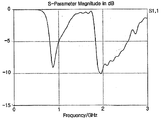
- FIG. 2 is a diagram illustrating S11 parameters of the antenna illustrated in FIG. 1.
- the S11 parameter of the antenna shown in FIG. 1 exhibits relatively wideband characteristics.
- a structure in which a large capacitive component value is obtained in a specific region along with the diversification of the capacitive component is preferable.
- a large capacitance value may be less affected by external factors such as a hand effect.
- FIG. 3 is a diagram illustrating a structure of a multi band internal antenna according to a second embodiment of the present invention.
- the multi band internal antenna includes a substrate 300, a radiation member 302 and an impedance matching / feeding unit 304 formed on the substrate 300.
- the impedance matching unit 304 may include a first matching member 320 and a second matching member 330.
- first coupling elements 306 are formed to protrude perpendicularly to the longitudinal direction of the first matching member 320, and a plurality of second coupling elements perpendicular to the longitudinal direction of the second matching member. 308 is formed to protrude.
- the first matching member 320 is electrically connected to the ground
- the second matching member 330 is electrically connected to the feed point
- the feeding is performed at the second matching member 330. Feeding by a coupling is performed to the first matching member 320.
- the multi-band internal antenna according to the second embodiment of the present invention shown in FIG. 3 is structured to allow coupling by higher capacitive components.
- the built-in antenna according to the second embodiment of the present invention has a structure in which a first coupling element 306 and a second coupling element 308 are added to the antenna structure according to the first embodiment.
- the first coupling element 306 and the second coupling element 308 allow for coupling matching by larger capacitive components.
- the first coupling element 306 and the second coupling element 308 protrude from the first matching member and the second matching member in the form of a comb.
- the first coupling element 306 and the second coupling element 308 are formed in a comb tooth shape and intersecting with each other.
- Such coupling elements 306 and 308 can substantially close the distance between the first matching member and the second matching member to enable acquisition of larger capacitive components as well as contribute to the diversification of the capacitive components. This allows for more broadband matching.
- FIG. 4 is a diagram illustrating S11 parameters of an antenna according to a second embodiment of the present invention.
- the antenna according to the second embodiment has better broadband characteristics than the antenna of the first embodiment shown in FIG. 2.
- the structure for securing a larger coupling between the radiating member and the ground member can be implemented in various ways in addition to the structures shown in FIGS. 1 and 3.
- 11 to 13 are diagrams illustrating structures of a first matching member and a second matching member for securing a large coupling according to an embodiment of the present invention.
- the width and length of the coupling element may be set to vary, and the coupling element may be implemented in a non-rectangular shape as shown in FIG. 13.
- FIG. 5 is a diagram illustrating a structure of a multi band internal antenna according to a third embodiment of the present invention.
- the multi-band internal antenna includes a substrate 500, a first radiating member 502 and an impedance matching / feeding unit 504 formed on the substrate 500. And a second radiating member 506.
- the impedance matching / feeding unit 504 includes a first matching member 520 electrically connected to the ground and a second matching member 530 electrically connected to the feed point, and the first matching member 520 and the first matching member 520.
- coupling elements 306 and 308 are formed to protrude to allow for more broadband matching.
- the first radiating member 502 extends from the first matching member 520 and is fed by a coupling.
- the configuration of the first radiation member 502 and the impedance matching unit 504 is the same as in the above-described second embodiment, and the second radiation member 506 is additionally provided.
- the second radiating member 506 is additionally provided to transmit and receive a signal of a different band from the first radiating member 502.
- the second radiating member 506 is spaced apart from the first radiating member 502 and the impedance matching / feeding unit 504 by a predetermined distance to be in electrical contact with each other.
- the second radiating member 506 is electrically connected to the ground, and power feeding is supplied by coupling from the impedance matching / feeding unit 504.
- FIG. 5 a case in which the second radiating member 506 is shorter than that of the first radiating member 502 is illustrated, and the second radiating member 506 is capable of receiving a signal having a high frequency band compared to the first radiating member 502. It is provided to transmit and receive.
- the second radiating member 506 is illustrated in FIG. 5 once bent, it will be apparent to those skilled in the art that the shape of the second radiating member is not limited thereto.
- FIG. 6 is a diagram illustrating S11 parameters of a multi band antenna according to the third embodiment of the present invention.
- the resonance point is formed in the high frequency band by additionally providing the second ground member 510.
- Two resonance points are formed in the high frequency band, and the additional resonance point is due to parasitic components.
- FIG. 7 is a diagram illustrating a structure of a multi band internal antenna according to a fourth embodiment of the present invention.
- a multi band internal antenna is formed on a substrate 700, a first radiating member 702 formed on the substrate 700, and the substrate 700.
- the impedance matching / feeding unit 704 includes a first matching member 720 and a second matching member 730, the first matching member 720 being electrically connected to ground, and the second matching member 730. Is electrically connected to the feed point.
- the first radiating member receives the RF signal through coupling feeding at the impedance matching / feeding unit.
- the second radiating member 706 is not fed by the coupling and is fed directly.
- the second radiating member 706 is electrically coupled with the second matching member 730 of the impedance matching / feeding unit 704 that is electrically connected to the feeding point to perform direct feeding.
- the radiation member when the radiation member is additionally provided for transmission and reception of signals in other bands, the radiation member may be fed by the coupler as in the third embodiment, and as in the fourth embodiment, direct feeding may be performed. It may be.
- FIG. 7 illustrates a case in which the second matching member 730 and the second radiating member 706 are electrically coupled on the substrate, but the second matching member 730 and the second radiating member 706 are necessarily coupled on the substrate. Need not be and may be electrically coupled in other areas.
- FIG. 8 is a diagram illustrating S11 parameters of a multi-band antenna according to the fourth embodiment of the present invention.
- FIG. 9 is a diagram illustrating a structure in which a multi band internal antenna according to a third embodiment of the present invention is coupled to an antenna carrier of a terminal.
- the antenna carrier includes a horizontal portion 900 and a vertical portion 902, the vertical portion 902 is formed perpendicular to the substrate 910 of the terminal to support the horizontal portion 900, the horizontal portion 900 It is formed parallel to the substrate of the terminal, the above-described elements are coupled to the horizontal portion 900.
- the first matching member extends to the vertical portion 902 to be coupled to the ground of the terminal substrate 910, and the second matching member extends to be electrically connected to the feed point.
- the second radiation member is extended to the vertical portion 902 to be coupled to the ground of the terminal substrate 910.
- FIG. 10 is a diagram illustrating a structure in which a multi band internal antenna according to a fourth embodiment of the present invention is coupled to a PCB of a terminal.
- the second radiating member and the second matching member connected to the feed point of the fourth embodiment are electrically coupled at a point A, and the second radiating member is directly fed with power.
Landscapes
- Details Of Aerials (AREA)
- Waveguide Aerials (AREA)
- Aerials With Secondary Devices (AREA)
Abstract
Priority Applications (4)
| Application Number | Priority Date | Filing Date | Title |
|---|---|---|---|
| US12/811,485 US8884836B2 (en) | 2008-01-08 | 2009-01-08 | Multi-band internal antenna |
| CN200980101818.XA CN101911388B (zh) | 2008-01-08 | 2009-01-08 | 多频段内置天线 |
| EP09700969.0A EP2242144B1 (fr) | 2008-01-08 | 2009-01-08 | Antenne intérieure multibande |
| JP2010542166A JP5777885B2 (ja) | 2008-01-08 | 2009-01-08 | 多重帯域内蔵型アンテナ |
Applications Claiming Priority (2)
| Application Number | Priority Date | Filing Date | Title |
|---|---|---|---|
| KR10-2008-0002266 | 2008-01-08 | ||
| KR20080002266 | 2008-01-08 |
Publications (2)
| Publication Number | Publication Date |
|---|---|
| WO2009088231A2 true WO2009088231A2 (fr) | 2009-07-16 |
| WO2009088231A3 WO2009088231A3 (fr) | 2009-10-22 |
Family
ID=40853604
Family Applications (1)
| Application Number | Title | Priority Date | Filing Date |
|---|---|---|---|
| PCT/KR2009/000095 Ceased WO2009088231A2 (fr) | 2008-01-08 | 2009-01-08 | Antenne intérieure multibande |
Country Status (6)
| Country | Link |
|---|---|
| US (1) | US8884836B2 (fr) |
| EP (1) | EP2242144B1 (fr) |
| JP (1) | JP5777885B2 (fr) |
| KR (1) | KR100985476B1 (fr) |
| CN (1) | CN101911388B (fr) |
| WO (1) | WO2009088231A2 (fr) |
Cited By (5)
| Publication number | Priority date | Publication date | Assignee | Title |
|---|---|---|---|---|
| JP2011061638A (ja) * | 2009-09-11 | 2011-03-24 | Tdk Corp | アンテナ装置 |
| WO2011046368A3 (fr) * | 2009-10-13 | 2011-08-04 | 주식회사 에이스테크놀로지 | Antenne intégrée à large bande utilisant un double couplage électromagnétique |
| KR101090114B1 (ko) | 2010-01-08 | 2011-12-07 | 주식회사 에이스테크놀로지 | 전자기 결합을 이용한 광대역 내장형 안테나 |
| CN102468531A (zh) * | 2010-11-04 | 2012-05-23 | 广达电脑股份有限公司 | 多频天线 |
| EP2375489A3 (fr) * | 2010-04-09 | 2014-11-26 | Sony Mobile Communications AB | Terminal mobile sans fil et dispositif d'antenne |
Families Citing this family (32)
| Publication number | Priority date | Publication date | Assignee | Title |
|---|---|---|---|---|
| KR100981883B1 (ko) * | 2008-04-30 | 2010-09-14 | 주식회사 에이스테크놀로지 | 지연파 구조를 이용한 광대역 내장형 안테나 |
| KR101075095B1 (ko) * | 2008-12-10 | 2011-10-19 | 주식회사 에이스테크놀로지 | 광대역 임피던스 매칭을 지원하는 내장형 안테나 |
| US20120026064A1 (en) * | 2009-04-14 | 2012-02-02 | Ace Technologies Corporation | Wideband antenna using coupling matching |
| KR101044615B1 (ko) * | 2009-04-27 | 2011-06-29 | 주식회사 에이스테크놀로지 | 전기적인 루프 형태의 신호선을 이용하는 광대역 안테나 |
| KR101043270B1 (ko) * | 2009-09-03 | 2011-06-21 | 주식회사 모비텍 | 인터디지트 커플링을 이용한 내장형 안테나 |
| KR101132616B1 (ko) * | 2009-09-23 | 2012-04-06 | 주식회사 이엠따블유 | 이중공진 평면 역에프 안테나 및 이를 포함하는 무선통신 단말기 |
| KR101094537B1 (ko) * | 2010-03-31 | 2011-12-19 | 주식회사 에이스앤파트너스 | 스파이럴 구조의 전자기 결합을 이용한 광대역 내장형 안테나 |
| KR101120864B1 (ko) * | 2010-03-31 | 2012-03-16 | 주식회사 에이스앤파트너스 | 개선된 임피던스 매칭을 지원하는 전자기 결합을 이용한 광대역 내장형 안테나 |
| KR101092094B1 (ko) * | 2010-05-13 | 2011-12-12 | 라디나 주식회사 | 확장된 그라운드를 이용한 광대역 안테나 |
| US8654020B2 (en) | 2010-08-25 | 2014-02-18 | Radina Co., Ltd | Antenna having capacitive element |
| KR101288159B1 (ko) | 2010-11-29 | 2013-07-18 | 주식회사 에이스테크놀로지 | 단말기 하우징에 결합되는 내장형 안테나 |
| CN102760940B (zh) * | 2011-04-29 | 2015-05-27 | 纬创资通股份有限公司 | 耦合式天线及具有耦合式天线的电子装置 |
| KR101634824B1 (ko) * | 2011-05-16 | 2016-06-29 | 라디나 주식회사 | 분기 캐패시터를 이용한 역-f 안테나 |
| TWI487198B (zh) * | 2011-06-03 | 2015-06-01 | Wistron Neweb Corp | 多頻天線 |
| CN102820523B (zh) * | 2011-06-07 | 2016-03-23 | 启碁科技股份有限公司 | 多频天线 |
| CN102891352B (zh) * | 2011-07-19 | 2015-04-29 | 深圳市信维通信股份有限公司 | 天线单元、具有它的天线和天线匹配装置 |
| KR101832961B1 (ko) * | 2011-10-05 | 2018-02-28 | 엘지전자 주식회사 | 이동 단말기 |
| US9178270B2 (en) * | 2012-05-17 | 2015-11-03 | Futurewei Technologies, Inc. | Wireless communication device with a multiband antenna, and methods of making and using thereof |
| CN103915682A (zh) * | 2013-01-06 | 2014-07-09 | 华为技术有限公司 | 印刷电路板天线和印刷电路板 |
| KR101438151B1 (ko) * | 2013-07-22 | 2014-09-04 | 순천향대학교 산학협력단 | 모바일 단말용 광대역 안테나 |
| CN104347926B (zh) * | 2013-07-31 | 2017-04-19 | 华为终端有限公司 | 一种印制天线和终端设备 |
| CN103647145A (zh) * | 2013-12-27 | 2014-03-19 | 禾邦电子(苏州)有限公司 | 宽频模块化天线及具有其的天线组件 |
| WO2015135188A1 (fr) * | 2014-03-13 | 2015-09-17 | 华为终端有限公司 | Antenne et borne |
| WO2016029404A1 (fr) * | 2014-08-28 | 2016-03-03 | 华为技术有限公司 | Appareil d'antenne et dispositif |
| WO2016065588A1 (fr) * | 2014-10-30 | 2016-05-06 | 华为技术有限公司 | Appareil d'antenne et terminal sans fil |
| US9363794B1 (en) * | 2014-12-15 | 2016-06-07 | Motorola Solutions, Inc. | Hybrid antenna for portable radio communication devices |
| CN106876903B (zh) * | 2017-04-10 | 2023-05-16 | 西安巨向导航科技有限公司 | 一种天线 |
| JP7216577B2 (ja) * | 2019-03-05 | 2023-02-01 | 日本航空電子工業株式会社 | アンテナ |
| JP7369545B2 (ja) * | 2019-05-24 | 2023-10-26 | 株式会社デンソーテン | アンテナ装置 |
| KR20230034696A (ko) | 2021-09-03 | 2023-03-10 | 삼성전자주식회사 | 안테나 및 마이크를 포함하는 전자 장치 |
| WO2024050994A1 (fr) * | 2022-09-08 | 2024-03-14 | 昆山睿翔讯通通信技术有限公司 | Antenne de terminal mobile et terminal mobile |
| KR20240066865A (ko) | 2022-11-08 | 2024-05-16 | 동우 화인켐 주식회사 | 안테나 구조체 |
Family Cites Families (26)
| Publication number | Priority date | Publication date | Assignee | Title |
|---|---|---|---|---|
| US2867126A (en) * | 1956-08-31 | 1959-01-06 | Clark Equipment Co | Transmission |
| JPH07193417A (ja) | 1993-12-27 | 1995-07-28 | Central Glass Co Ltd | ガラスアンテナ |
| WO1996029756A1 (fr) * | 1995-03-20 | 1996-09-26 | Minnesota Mining And Manufacturing Company | Antenne a deux frequences avec diplexeur integre |
| JP3319268B2 (ja) * | 1996-02-13 | 2002-08-26 | 株式会社村田製作所 | 表面実装型アンテナおよびこれを用いた通信機 |
| JP3114605B2 (ja) | 1996-02-14 | 2000-12-04 | 株式会社村田製作所 | 表面実装型アンテナおよびこれを用いた通信機 |
| JP3114621B2 (ja) * | 1996-06-19 | 2000-12-04 | 株式会社村田製作所 | 表面実装型アンテナおよびこれを用いた通信機 |
| TW423180B (en) | 1997-01-31 | 2001-02-21 | Terajima Fumitaka | Glass antenna device for an automobile |
| JP3700372B2 (ja) | 1997-01-31 | 2005-09-28 | 旭硝子株式会社 | 車両用ガラスアンテナ装置 |
| CN1141756C (zh) | 1999-09-30 | 2004-03-10 | 株式会社村田制作所 | 表面安装型天线和包括它的通信装置 |
| US20010050643A1 (en) * | 2000-02-22 | 2001-12-13 | Igor Egorov | Small-size broad-band printed antenna with parasitic element |
| JP3468201B2 (ja) * | 2000-03-30 | 2003-11-17 | 株式会社村田製作所 | 表面実装型アンテナおよびその複共振の周波数調整設定方法および表面実装型アンテナを備えた通信装置 |
| JP3658639B2 (ja) * | 2000-04-11 | 2005-06-08 | 株式会社村田製作所 | 表面実装型アンテナおよびそのアンテナを備えた無線機 |
| US6337667B1 (en) * | 2000-11-09 | 2002-01-08 | Rangestar Wireless, Inc. | Multiband, single feed antenna |
| EP1376761B1 (fr) * | 2001-03-15 | 2007-11-14 | Matsushita Electric Industrial Co., Ltd. | Dispositif d'antenne |
| JP2003258527A (ja) * | 2002-02-27 | 2003-09-12 | Toyota Central Res & Dev Lab Inc | アンテナ |
| WO2004057698A2 (fr) * | 2002-12-17 | 2004-07-08 | Ethertronics, Inc. | Antennes a encombrement reduit et performance amelioree |
| JP2004236273A (ja) * | 2003-02-03 | 2004-08-19 | Matsushita Electric Ind Co Ltd | アンテナ |
| US6914562B2 (en) * | 2003-04-10 | 2005-07-05 | Avery Dennison Corporation | RFID tag using a surface insensitive antenna structure |
| US7119743B2 (en) * | 2003-06-09 | 2006-10-10 | Matsushita Electric Industrial Co., Ltd. | Antenna and electronic device using the same |
| DE60319965T2 (de) * | 2003-06-12 | 2009-04-30 | Research In Motion Ltd., Waterloo | Mehrelement-Antenne mit parasitärem Antennenelement |
| FI120606B (fi) * | 2003-10-20 | 2009-12-15 | Pulse Finland Oy | Sisäinen monikaista-antenni |
| US7317901B2 (en) * | 2004-02-09 | 2008-01-08 | Motorola, Inc. | Slotted multiple band antenna |
| KR100649495B1 (ko) * | 2004-09-06 | 2006-11-24 | 삼성전기주식회사 | 안테나 모듈 및 이를 구비한 전자 장치 |
| JP2006197254A (ja) * | 2005-01-13 | 2006-07-27 | Sakae Riken Kogyo Co Ltd | 自動車用アンテナ |
| KR100787229B1 (ko) * | 2005-02-04 | 2007-12-21 | 삼성전자주식회사 | 이중 대역 역 에프 평판안테나 |
| JP4578411B2 (ja) * | 2005-07-22 | 2010-11-10 | ブラザー工業株式会社 | アンテナ及び無線タグ |
-
2009
- 2009-01-08 US US12/811,485 patent/US8884836B2/en active Active
- 2009-01-08 KR KR1020090001577A patent/KR100985476B1/ko not_active Expired - Fee Related
- 2009-01-08 EP EP09700969.0A patent/EP2242144B1/fr not_active Not-in-force
- 2009-01-08 WO PCT/KR2009/000095 patent/WO2009088231A2/fr not_active Ceased
- 2009-01-08 JP JP2010542166A patent/JP5777885B2/ja not_active Expired - Fee Related
- 2009-01-08 CN CN200980101818.XA patent/CN101911388B/zh not_active Expired - Fee Related
Non-Patent Citations (2)
| Title |
|---|
| None |
| See also references of EP2242144A4 |
Cited By (5)
| Publication number | Priority date | Publication date | Assignee | Title |
|---|---|---|---|---|
| JP2011061638A (ja) * | 2009-09-11 | 2011-03-24 | Tdk Corp | アンテナ装置 |
| WO2011046368A3 (fr) * | 2009-10-13 | 2011-08-04 | 주식회사 에이스테크놀로지 | Antenne intégrée à large bande utilisant un double couplage électromagnétique |
| KR101090114B1 (ko) | 2010-01-08 | 2011-12-07 | 주식회사 에이스테크놀로지 | 전자기 결합을 이용한 광대역 내장형 안테나 |
| EP2375489A3 (fr) * | 2010-04-09 | 2014-11-26 | Sony Mobile Communications AB | Terminal mobile sans fil et dispositif d'antenne |
| CN102468531A (zh) * | 2010-11-04 | 2012-05-23 | 广达电脑股份有限公司 | 多频天线 |
Also Published As
| Publication number | Publication date |
|---|---|
| KR20090076839A (ko) | 2009-07-13 |
| JP2011509624A (ja) | 2011-03-24 |
| US8884836B2 (en) | 2014-11-11 |
| EP2242144A2 (fr) | 2010-10-20 |
| WO2009088231A3 (fr) | 2009-10-22 |
| EP2242144B1 (fr) | 2020-08-19 |
| EP2242144A4 (fr) | 2013-11-06 |
| CN101911388B (zh) | 2014-04-09 |
| CN101911388A (zh) | 2010-12-08 |
| JP5777885B2 (ja) | 2015-09-09 |
| KR100985476B1 (ko) | 2010-10-05 |
| US20110181487A1 (en) | 2011-07-28 |
Similar Documents
| Publication | Publication Date | Title |
|---|---|---|
| WO2009088231A2 (fr) | Antenne intérieure multibande | |
| WO2009145437A2 (fr) | Antenne intégrée pour prendre en charge l'adaptation d'impédance pour le mode multibande | |
| WO2009134013A2 (fr) | Antenne interne à large bande utilisant une structure à ondes lentes | |
| CN1248359C (zh) | 平衡可伸缩移动电话天线 | |
| FI113911B (fi) | Menetelmä signaalin kytkemiseksi ja antennirakenne | |
| US9525212B2 (en) | Feeding network, antenna, and dual-polarized antenna array feeding circuit | |
| JP3864127B2 (ja) | デュアルフィーディングポートを有するマルチバンドチップアンテナ及びこれを用いる移動通信装置 | |
| WO2010119999A1 (fr) | Antenne a large bande dotée d'une adaptation couplée avec l'extrémité court-circuitée d'un émetteur | |
| WO2010119998A1 (fr) | Antenne large bande mettant en oeuvre l'appariement par couplage | |
| TWI356528B (fr) | ||
| EP1776736A1 (fr) | Systeme d'antenne multibande | |
| WO2010030128A2 (fr) | Antenne multibande utilisant un couplage électromagnétique | |
| CN101388494B (zh) | 多天线整合模组 | |
| WO2012026635A1 (fr) | Antenne dotée d'un élément capacitif | |
| WO2011122821A2 (fr) | Antenne interne à large bande utilisant un couplage électromagnétique supportant une correspondance d'impédance améliorée | |
| TWI446626B (zh) | 寬頻行動通訊天線 | |
| WO2009154376A2 (fr) | Dispositif d'antenne pour combiné | |
| JP2006238029A (ja) | 携帯無線機 | |
| CN201163659Y (zh) | 具有蛇形线结构的平面倒f天线 | |
| WO2007084051A1 (fr) | Agencement d’antenne pour une pluralite de bandes de frequences | |
| CN205509010U (zh) | 天线装置及移动终端 | |
| WO2008079396A1 (fr) | Antenne en cercle | |
| WO2016064080A1 (fr) | Antenne multibande à deux ports | |
| WO2010071265A1 (fr) | Antenne incorporée capable d'appariement d'impédance large bande et comportant une plaque couplée à un substrat | |
| WO2012105772A2 (fr) | Module haute fréquence multimode |
Legal Events
| Date | Code | Title | Description |
|---|---|---|---|
| WWE | Wipo information: entry into national phase |
Ref document number: 200980101818.X Country of ref document: CN |
|
| 121 | Ep: the epo has been informed by wipo that ep was designated in this application |
Ref document number: 09700969 Country of ref document: EP Kind code of ref document: A2 |
|
| WWE | Wipo information: entry into national phase |
Ref document number: 4011/CHENP/2010 Country of ref document: IN |
|
| WWE | Wipo information: entry into national phase |
Ref document number: 2009700969 Country of ref document: EP |
|
| WWE | Wipo information: entry into national phase |
Ref document number: 2010542166 Country of ref document: JP |
|
| NENP | Non-entry into the national phase |
Ref country code: DE |
|
| WWE | Wipo information: entry into national phase |
Ref document number: 12811485 Country of ref document: US |