WO2009090713A1 - Dispositif à ondes acoustiques de surface - Google Patents
Dispositif à ondes acoustiques de surface Download PDFInfo
- Publication number
- WO2009090713A1 WO2009090713A1 PCT/JP2008/003882 JP2008003882W WO2009090713A1 WO 2009090713 A1 WO2009090713 A1 WO 2009090713A1 JP 2008003882 W JP2008003882 W JP 2008003882W WO 2009090713 A1 WO2009090713 A1 WO 2009090713A1
- Authority
- WO
- WIPO (PCT)
- Prior art keywords
- film thickness
- sio
- film
- idt
- acoustic wave
- Prior art date
- Legal status (The legal status is an assumption and is not a legal conclusion. Google has not performed a legal analysis and makes no representation as to the accuracy of the status listed.)
- Ceased
Links
Images






Classifications
-
- H—ELECTRICITY
- H03—ELECTRONIC CIRCUITRY
- H03H—IMPEDANCE NETWORKS, e.g. RESONANT CIRCUITS; RESONATORS
- H03H9/00—Networks comprising electromechanical or electro-acoustic elements; Electromechanical resonators
- H03H9/02—Details
- H03H9/02535—Details of surface acoustic wave devices
- H03H9/02543—Characteristics of substrate, e.g. cutting angles
- H03H9/02559—Characteristics of substrate, e.g. cutting angles of lithium niobate or lithium-tantalate substrates
-
- H—ELECTRICITY
- H03—ELECTRONIC CIRCUITRY
- H03H—IMPEDANCE NETWORKS, e.g. RESONANT CIRCUITS; RESONATORS
- H03H9/00—Networks comprising electromechanical or electro-acoustic elements; Electromechanical resonators
- H03H9/02—Details
- H03H9/02535—Details of surface acoustic wave devices
- H03H9/02543—Characteristics of substrate, e.g. cutting angles
- H03H9/02574—Characteristics of substrate, e.g. cutting angles of combined substrates, multilayered substrates, piezoelectrical layers on not-piezoelectrical substrate
-
- H—ELECTRICITY
- H03—ELECTRONIC CIRCUITRY
- H03H—IMPEDANCE NETWORKS, e.g. RESONANT CIRCUITS; RESONATORS
- H03H9/00—Networks comprising electromechanical or electro-acoustic elements; Electromechanical resonators
- H03H9/02—Details
- H03H9/125—Driving means, e.g. electrodes, coils
- H03H9/145—Driving means, e.g. electrodes, coils for networks using surface acoustic waves
- H03H9/14538—Formation
Definitions
- the present invention relates to a surface acoustic wave device used as, for example, a resonator or a bandpass filter, and more particularly to a surface acoustic wave device having a structure in which an IDT made of Cu filled in a groove on a piezoelectric substrate is formed. .
- Patent Document 1 discloses a surface acoustic wave device 1001 schematically showing a cross-sectional structure in FIG.
- a plurality of grooves 1002 b are formed on the upper surface 1002 a of the LiTaO 3 substrate 1002.
- a plurality of grooves 1002b are filled with a metal, whereby an IDT 1003 having a plurality of electrode fingers made of the metal is formed.
- a SiO 2 film 1004 is laminated so as to cover the upper surface 1002a of the LiTaO 3 substrate 1002. Since the LiTaO 3 substrate 1002 has a negative frequency temperature coefficient TCF, an SiO 2 film 1004 having a positive frequency temperature coefficient TCF is laminated, and the absolute value of the frequency temperature coefficient TCF of the surface acoustic wave device 1001 is reduced. .
- a large reflection coefficient can be obtained in the IDT by forming the IDT using a metal embedded in the plurality of grooves 1002b.
- the reflection coefficient per electrode finger is It is shown that 0.05 is obtained, and a larger reflection coefficient is obtained as the electrode thickness is larger.
- Patent Document 2 discloses a surface acoustic wave device shown in FIG.
- an IDT 1103 is formed on a piezoelectric substrate 1102 made of LiTaO 3 or LiNbO 3 .
- a protective film 1104 is formed so as to cover the IDT 1103.
- a first insulating layer 1105 made of SiO 2 equal to the thickness of the laminated metal film formed by laminating the IDT 1103 and the protective film 1104 is formed in the remaining region excluding the portion where the IDT 1103 and the protective film 1104 are formed.
- a second insulator layer 1106 made of SiO 2 is laminated so as to cover the first insulator layer 1105.
- the absolute value of the reflection coefficient can be increased as the thickness of the IDT made of Al is increased.
- the inventor of the present application has found that good resonance characteristics cannot be obtained simply by increasing the absolute value of the reflection coefficient. That is, in the surface acoustic wave device described in Patent Document 1, the absolute value of the reflection coefficient can be increased by increasing the thickness of the electrode made of Al.
- the sign of the reflection coefficient is negative, there are many in the passband. It has been found that ripples are generated and good resonance characteristics cannot be obtained.
- Patent Document 1 the relationship between the thickness of the IDT and the reflection coefficient is merely described for the case where an IDT made of Al is used on a LiTaO 3 substrate. Note that paragraph 0129 of Patent Document 1 suggests that an IDT may be formed using another metal such as Au on a LiNbO 3 substrate, but only an IDT made of Au is disclosed.
- Patent Document 2 when an IDT made of a metal having a density higher than that of Al is used, it is shown that the absolute value of the reflection coefficient can be increased. No particular mention is made of increasing the electromechanical coupling coefficient.
- the Euler angle range of the LiNbO 3 substrate that can be used to obtain a sufficiently large electromechanical coupling coefficient k 2 is narrow. There was a problem.
- the object of the present invention is to eliminate the drawbacks of the prior art, use a LiNbO 3 substrate as a piezoelectric substrate, and not only have a sufficiently large reflection coefficient of IDT, but also a large electromechanical coupling coefficient k 2.
- An object of the present invention is to provide a surface acoustic wave device in which the Euler angle range of a LiNbO 3 substrate that can be used is relatively wide and the degree of freedom in design can be increased.
- a piezoelectric substrate made of a LiNbO 3 substrate and having a plurality of grooves formed on the upper surface thereof, and a plurality of electrode fingers made of a metal material filled in the plurality of grooves on the upper surface of the piezoelectric substrate.
- the metal material is made of Cu or an alloy mainly containing Cu.
- the electrode film thickness of the IDT and the Euler angles of the LiNbO 3 substrate (0 ° ⁇ 10 °, ⁇ , 0 ° ⁇ 10 ° ) Is one of the combinations shown in Table 1 below.
- the Euler angle range of the LiNbO 3 substrate capable of obtaining a large electromechanical coupling coefficient k 2 can be further expanded.
- the surface acoustic wave device preferably further includes a dielectric film made of an inorganic material mainly composed of SiO 2 or SiO 2 that covers the IDT and the piezoelectric substrate.
- the frequency temperature coefficient of the dielectric film made of an inorganic material mainly composed of SiO 2 or SiO 2 is a positive value
- the frequency temperature coefficient TCF of LiNbO 3 is a negative value.
- a surface acoustic wave device having a small absolute value of the frequency temperature coefficient TCF can be provided.
- the normalized thickness is normalized by ⁇ of the IDT, and the ⁇ of the SiO 2 film as the dielectric film is specified.
- the normalized film thickness and the Euler angle (0 ° ⁇ 10 °, ⁇ , 0 ° ⁇ 10 °) of the LiNbO 3 substrate are one of the combinations shown in Tables 2 to 4 below. is there.
- the metal material is made of the specific metal.
- a large electromechanical coupling coefficient k 2 can be obtained.
- the Euler angle of the LiNbO 3 substrate can be selected from a wide range in order to realize a range where the electromechanical coupling coefficient k 2 is large. Therefore, not only can the characteristics of the surface acoustic wave device be improved, but also the degree of freedom in designing the surface acoustic wave device can be increased.
- FIGS. 1A and 1B are schematic partial front sectional views showing the main part of a surface acoustic wave device according to an embodiment of the present invention
- FIG. 1B is a schematic plan view of the surface acoustic wave device.
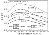
- FIG. FIG. 2 shows the relationship between the Euler angle ⁇ and the reflection coefficient when Cu is used as the metal material constituting the IDT in one embodiment of the present invention, and the solid line indicates a structure in which SiO 2 films are laminated.
- FIG. 6 is a diagram showing the results in the case where the broken line indicates a structure in which the SiO 2 film is not laminated.
- FIG. 3 shows the relationship between the Euler angle ⁇ and the electromechanical coupling coefficient k 2 when Cu is used as the metal material constituting the IDT in one embodiment of the present invention, and the solid line indicates the lamination of the SiO 2 film.
- FIG. 6 is a diagram showing the result in the case of a structure in which a broken line indicates the result in the case of a structure in which an SiO 2 film is not laminated.
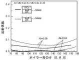
- FIG. 4 shows the relationship between the Euler angle ⁇ and the reflection coefficient when Al is used as the metal material constituting the IDT in the conventional example, and the solid line shows the result in the case where the SiO 2 film is laminated.
- FIG. 6 is a diagram showing a result in a case where a broken line has a structure in which an SiO 2 film is not laminated.
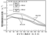
- FIG. 5 shows the relationship between Euler angle ⁇ and electromechanical coupling coefficient k 2 when Al is used as the metal material constituting IDT in the conventional example, and the solid line is a structure in which SiO 2 films are laminated.
- FIG. 6 is a diagram showing the results in the case where the broken line indicates a structure in which the SiO 2 film is not laminated.
- FIG. 6 shows the relationship between the Euler angle ⁇ and the reflection coefficient when Au is used as the metal material constituting the IDT in the conventional example, and the solid line shows the result in the case where the SiO 2 film is laminated.
- FIG. 5 shows the relationship between Euler angle ⁇ and electromechanical coupling coefficient k 2 when Al is used as the metal material constituting IDT in the conventional example, and the solid line is a structure in which SiO 2 films are laminated.
- FIG. 6 is a diagram showing
- FIG. 6 is a diagram showing a result in a case where a broken line has a structure in which an SiO 2 film is not laminated.
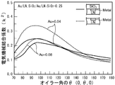
- FIG. 7 shows the relationship between the Euler angle ⁇ and the electromechanical coupling coefficient k 2 when Au is used as the metal material constituting the IDT in the conventional example, and the solid line is a structure in which the SiO 2 film is laminated.
- FIG. 6 is a diagram showing the results in the case where the broken line indicates a structure in which the SiO 2 film is not laminated.
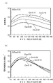
- 8A and 8B show the normalized film thickness of the Cu film and Euler when Cu is used as the metal material constituting the IDT and the SiO 2 film is not formed in one embodiment of the present invention.
- FIGS. 9A and 9B show a Cu film in the case where Cu is used as the metal material constituting the IDT and the normalized film thickness of the SiO 2 film is 0.05 in one embodiment of the present invention. and the normalized film thickness is a graph showing respective relationships between ⁇ of the Euler angles, the reflection coefficient and the electromechanical coupling coefficient k 2.
- 10 (a) and 10 (b) show the Cu film in the case where Cu is used as the metal material constituting the IDT and the normalized film thickness of the SiO 2 film is 0.1 in one embodiment of the present invention.
- the normalized film thickness is a graph showing respective relationships between ⁇ of the Euler angles, the reflection coefficient and the electromechanical coupling coefficient k 2.
- 11 (a) and 11 (b) show the Cu film in the case where Cu is used as the metal material constituting the IDT and the normalized film thickness of the SiO 2 film is 0.15 in one embodiment of the present invention. and the normalized film thickness is a graph showing respective relationships between ⁇ of the Euler angles, the reflection coefficient and the electromechanical coupling coefficient k 2.
- 12 (a) and 12 (b) show the Cu film in the case where Cu is used as the metal material constituting the IDT and the normalized film thickness of the SiO 2 film is 0.2 in one embodiment of the present invention.
- FIGS. 13A and 13B show the Cu film in the case where Cu is used as the metal material constituting the IDT and the normalized film thickness of the SiO 2 film is 0.25 in one embodiment of the present invention. and the normalized film thickness is a graph showing respective relationships between ⁇ of the Euler angles, the reflection coefficient and the electromechanical coupling coefficient k 2.
- 14 (a) and 14 (b) show the Cu film in the case where Cu is used as the metal material constituting the IDT and the normalized film thickness of the SiO 2 film is 0.3 in one embodiment of the present invention.
- FIGS. 15A and 15B show the Cu film in the case where Cu is used as the metal material constituting the IDT and the normalized film thickness of the SiO 2 film is 0.35 in one embodiment of the present invention. and the normalized film thickness is a graph showing respective relationships between ⁇ of the Euler angles, the reflection coefficient and the electromechanical coupling coefficient k 2.
- FIG. 16 is a schematic front sectional view for explaining an example of a conventional surface acoustic wave device.
- FIG. 17 is a partially cutaway front sectional view showing another example of a conventional surface acoustic wave device.
- the surface acoustic wave device 2 ... LiNbO 3 substrate 2a ... top 2b ... groove 3 ... IDT 4 ... SiO 2 film 5,6 ... Reflector
- FIGS. 1A and 1B are schematic partial front sectional views of a portion where an IDT of a surface acoustic wave device according to a first embodiment of the present invention is formed, and FIG. It is a schematic plan view of a surface acoustic wave device.
- the surface acoustic wave device 1 includes a LiNbO 3 substrate 2.
- a plurality of grooves 2 b are formed on the upper surface 2 a of the LiNbO 3 substrate 2.
- the IDT 3 having a plurality of electrode fingers is formed by filling the plurality of grooves 2b with metal.
- the upper surface of the IDT 3 and the upper surface 2a of the LiNbO 3 substrate 2 are flush with each other.
- a SiO 2 film 4 is formed so as to cover the upper surface 2a and the IDT 3. In the present invention, the SiO 2 film 4 may not be formed.
- the surface acoustic wave device 1 has the IDT 3 and first and second reflectors 5 and 6 disposed on both sides of the IDT 3 in the surface wave propagation direction.
- This is a surface acoustic wave resonator.
- Each of the reflectors 5 and 6 is a grating reflector formed by short-circuiting both ends of a plurality of electrode fingers.
- the reflectors 5 and 6 are also formed by filling a plurality of grooves provided on the upper surface 2 a of the LiNbO 3 substrate 2 with the same metal. Therefore, also in the reflectors 5 and 6, the electrode surface and the upper surface 2a of the LiNbO 3 substrate 2 are substantially flush with each other. Therefore, the upper surface of the SiO 2 film 4 is substantially flattened over the entire surface acoustic wave device 1.
- the frequency temperature coefficient TCF of the LiNbO 3 substrate 2 is a negative value
- the frequency temperature coefficient TCF of the SiO 2 film 4 is a positive value
- the absolute value of the frequency temperature coefficient TCF is reduced as a whole. Therefore, in the surface acoustic wave device 1, the change in the frequency characteristics due to the temperature change is small.
- the surface acoustic wave device 1 is a surface acoustic wave device using SH waves, and is characterized in that the metal material constituting the IDT 3 is made of Cu or an alloy mainly composed of Cu. It is in.
- the IDT 3 may be added with a metal layer made of another metal material such as an adhesion layer and a diffusion prevention layer, or the IDT 3 may have a laminated structure with another metal layer.
- the surface acoustic wave device 1 of the present embodiment not only the absolute value of the reflection coefficient of the IDT 3 is increased, but also a large electromechanical coupling coefficient k 2 can be obtained. Also, the following concrete experimental examples of, as shown in, in obtaining an electromechanical coupling coefficient k 2 is large SAW device 1, it is possible to widen the Euler angle range of the LiNbO 3 substrate that may be utilized. Therefore, the degree of freedom in design can be increased. This will be described with reference to FIGS.
- the electromechanical coupling coefficient k 2 can be increased to 0.2 or more.
- the reflection coefficient is 0.1 or less regardless of the Euler angle ⁇ and the film thickness of the IDT made of Al. I understand that it is small.
- FIGS. 6 and 7 show the results when Au having a normalized film thickness of 0.04 or 0.08 standardized by the surface wave wavelength ⁇ is used as the electrode material. That is, the result when the IDT electrode 3 and the reflectors 5 and 6 shown in FIG. 1 are made of Au is shown.
- Figure 6 shows the relationship between ⁇ and the reflection coefficient of the Euler angles
- FIG. 7 shows the relationship between ⁇ and the electromechanical coupling coefficient k 2 of the Euler angles.
- the reflection coefficient can be increased regardless of the Euler angle ⁇ as compared with the case where the electrode material Al shown in FIG. 4 is used. .
- the normalized film thickness of the electrode made of Au is 0.
- the structure in which the SiO 2 film 4 is not formed is in the range of 72 ° to 131 °, and when the normalized film thickness of the electrode made of Au is 0.08, 85 ° to 119. It is in the range of °. Accordingly, when the normalized film thickness is changed in the range of 0.04 to 0.08, unless the Euler angle ⁇ is selected in the range of 85 ° to 119 °, the electromechanical coupling coefficient k 2 It can be seen that cannot be made 0.2 or more.
- the normalized film thickness of the Au film is 0 for the electromechanical coupling coefficient k 2 to be 0.2 or more. .04, the Euler angle ⁇ must be in the range of 77 ° to 117 °, and when the normalized film thickness is 0.08, the Euler angle ⁇ must be 90 ° to 114 °. Recognize. Therefore, it can be seen that when the normalized film thickness of the SiO 2 film 4 is in the range of 0.04 to 0.08, the Euler angle ⁇ must be in the range of 90 ° to 114 °.
- the range can be expanded. Accordingly, the degree of freedom in designing the surface acoustic wave device can be increased.
- the electromechanical coupling coefficient k 2 is 0.2 or more, to that to be good, in the surface acoustic wave device used as resonators and band filters, to obtain a bandwidth that is usually sought, electrical This is because the mechanical coupling coefficient k 2 is preferably about 0.2 or more.
- 2 and 3 are views showing a ⁇ of Euler angles, the relationship between the reflection coefficient and the electromechanical coupling coefficient k 2. 2 and 3, the normalized film thickness of Cu as the metal material constituting the IDT 3 and the reflectors 5 and 6 is set to 0.02, 0.04, or 0.08. Further, also in FIG. 2 and FIG. 3 shows the results when the SiO 2 film 4 is formed by a solid line in the solid line, the results when the SiO 2 film 4 is not formed by a broken line.
- the Euler angle range in which the electromechanical coupling coefficient k 2 can be 0.2 or more has a normalized film thickness of 0.
- the range may be in the range of 70 ° to 145 °.
- the range may be in the range of 70 ° to 151 °.
- the range of 70 ° to 156 ° is sufficient.
- the Euler angle ⁇ is 70 ° or more and 145 ° or less, more than 0.04 ⁇ , and 0.08 ⁇ or less. In this case, it is understood that the range may be 70 ° or more and 151 ° or less. Therefore, the range of Euler angle ⁇ can be expanded compared to the range of 85 ° or more and 119 ° or less when Au is used. Similarly, in the structure in which the SiO 2 film 4 is laminated, the Euler angle range in which the electromechanical coupling coefficient k 2 can be expanded to 0.2 or more is shown in FIG. 3 when the Cu film thickness is 0.02 ⁇ .
- the angle When the film thickness is 0.04 ⁇ , the angle may be 82 ° to 137 °, and when the film thickness is 0.08 ⁇ , the angle may be 79 ° to 124 °. That is, when the film thickness of Cu is in the range of 0.02 ⁇ to 0.04 ⁇ , the Euler angle ⁇ is 83 ° or more and 124 ° or less, more than 0.04 ⁇ , and 0.08 ⁇ or less. It can be seen that the angle may be 82 ° or more and 124 ° or less. Therefore, it can be seen that the Euler angle ⁇ range can be expanded compared to the range of 90 ° or more and 114 ° or less when the Au film is used.
- a metallic material electromechanical coupling coefficient k 2 constitutes the electrode is 0.2 or more, and the electrode film thickness made of the metal material, the Euler angles
- the combination of ⁇ is one of the combinations shown in Table 5 below. Table 5 shows the result in the case of the structure in which the SiO 2 film is not laminated.
- Table 5 also shows the case where Au is used as the metal material for comparison.
- the present inventors have further in the formed structure so as to cover the IDT electrode of the SiO 2 film as the dielectric film, also considered an electrode material, in addition to the electrode film thickness, the normalized thickness of the SiO 2 film Then, the range of each Euler angle ⁇ in which the electromechanical coupling coefficient k 2 is 0.2 or more was examined. A result is demonstrated for every metal material below.
- FIGS. 8 (a), (b) to 15 (a), (b) show the Euler angles ⁇ and Cu when the metal material is Cu and the SiO 2 film is formed with various normalized film thicknesses. illustrates the reflection coefficient and the relationship between the electromechanical coupling coefficient k 2, respectively.
- FIG. 8 (a), (b) shows the results when the normalized thickness of the SiO 2 film is 0, i.e. no SiO 2 film is formed
- FIGS. 9 to 15 the SiO 2 film The results are shown when the normalized film thicknesses are 0.05, 0.1, 0.15, 0.2, 0.25, 0.3, and 0.35, respectively.
- the standardized film thickness of Cu as the metal material constituting the IDT 3 and the reflectors 5 and 6 was set to various thicknesses as described in FIGS.
- FIG. 2 described above when Cu is used as the metal material, a larger reflection coefficient can be obtained than when Al is used regardless of the Euler angle ⁇ range.
- 8A to 15A also show that a large reflection coefficient is obtained even when the Cu film is variously changed regardless of the value of Euler angle ⁇ .
- the normalized film thickness of Cu is in the range of 0.04 to 0.08
- the normalized film thickness of the SiO 2 film is , if one of the combinations showing the range of ⁇ of Euler angles shown in Table 6 below, the electromechanical coefficient k 2 it can be seen that a 0.2 or higher.
- Table 6 below shows the lower limit value and upper limit value of the Euler angle ⁇ range.
- the Euler angle ⁇ should be in the range of 70 ° or more and 151 ° or less.
- the SiO 2 film thickness and Euler angle ⁇ range is one of the combinations shown in Table 7 below.
- the normalized film thickness of the Cu film is greater than 0.12 and less than or equal to 0.16
- the normalized film thickness of the SiO 2 film and the range of the Euler angle ⁇ are shown in the table below. if one of combinations shown in 8, likewise the electromechanical coefficient k 2 may be 0.2 or more. Tables 6 to 8 are based on the results of FIGS. 8 to 15 described above.
- the metal material is not limited to Cu described above, but may be an alloy mainly composed of Cu.
- SiO 2 film although SiO 2 film is formed is not limited to the SiO 2 film may be a dielectric film made of an inorganic material mainly containing SiO 2 film.
- these dielectric films have a positive frequency temperature coefficient, the absolute value of the frequency temperature coefficient of the surface acoustic wave device can be obtained by combining with a LiNbO 3 substrate having a negative frequency temperature coefficient. The value can be reduced. That is, a surface acoustic wave device having excellent temperature characteristics can be provided.
- the electrode structure of the surface acoustic wave device formed according to the present invention is not limited to that shown in FIG. 1, and the present invention is applied to surface acoustic wave resonators and surface acoustic wave filters having various electrode structures. be able to.
- the Euler angles ( ⁇ , ⁇ , ⁇ ) of LiTaO 3 are not particularly limited, but in order to use Rayleigh waves and SH waves as surface waves, Euler angles are used. It is desirable that ⁇ is in the range of 0 ° ⁇ 10 °, ⁇ is in the range of 70 ° to 180 °, and ⁇ is in the range of 0 ° ⁇ 10 °. That is, the Rayleigh wave and the SH wave can be suitably used by setting the Euler angle to a range of (0 ° ⁇ 10 °, 70 ° to 180 °, 0 ° ⁇ 10 °). More specifically, SH waves can be used more suitably at (0 ° ⁇ 10 °, 90 ° to 180 °, 0 ° ⁇ 10 °).
- an LSAW wave may be used, and in that case, the Euler angles may be in the range of (0 ° ⁇ 10 °, 110 ° to 160 °, 0 ° ⁇ 10 °).
- the electrode structure of the 1-port SAW resonator is shown.
- the surface acoustic wave device of the present invention is widely applied to other resonator structures or other resonator surface acoustic wave filters. Can do.
Landscapes
- Physics & Mathematics (AREA)
- Acoustics & Sound (AREA)
- Chemical & Material Sciences (AREA)
- Engineering & Computer Science (AREA)
- Materials Engineering (AREA)
- Surface Acoustic Wave Elements And Circuit Networks Thereof (AREA)
Abstract
Priority Applications (2)
| Application Number | Priority Date | Filing Date | Title |
|---|---|---|---|
| CN2008801246798A CN101911482B (zh) | 2008-01-17 | 2008-12-22 | 弹性表面波装置 |
| JP2009549908A JPWO2009090713A1 (ja) | 2008-01-17 | 2008-12-22 | 弾性表面波装置 |
Applications Claiming Priority (4)
| Application Number | Priority Date | Filing Date | Title |
|---|---|---|---|
| JP2008008350 | 2008-01-17 | ||
| JP2008-008350 | 2008-01-17 | ||
| JP2008207765 | 2008-08-12 | ||
| JP2008-207765 | 2008-08-12 |
Publications (1)
| Publication Number | Publication Date |
|---|---|
| WO2009090713A1 true WO2009090713A1 (fr) | 2009-07-23 |
Family
ID=40885124
Family Applications (1)
| Application Number | Title | Priority Date | Filing Date |
|---|---|---|---|
| PCT/JP2008/003882 Ceased WO2009090713A1 (fr) | 2008-01-17 | 2008-12-22 | Dispositif à ondes acoustiques de surface |
Country Status (3)
| Country | Link |
|---|---|
| JP (1) | JPWO2009090713A1 (fr) |
| CN (1) | CN101911482B (fr) |
| WO (1) | WO2009090713A1 (fr) |
Cited By (1)
| Publication number | Priority date | Publication date | Assignee | Title |
|---|---|---|---|---|
| WO2018092470A1 (fr) * | 2016-11-17 | 2018-05-24 | 株式会社村田製作所 | Dispositif à ondes acoustiques |
Citations (4)
| Publication number | Priority date | Publication date | Assignee | Title |
|---|---|---|---|---|
| JPS5248375U (fr) * | 1975-10-02 | 1977-04-06 | ||
| JPH0237815A (ja) * | 1988-07-27 | 1990-02-07 | Fujitsu Ltd | 弾性表面波素子 |
| JPH0983030A (ja) * | 1995-09-11 | 1997-03-28 | Matsushita Electric Ind Co Ltd | 弾性表面波素子及びその製造方法 |
| WO2006011417A1 (fr) * | 2004-07-26 | 2006-02-02 | Murata Manufacturing Co., Ltd. | Dispositif à onde acoustique de surface |
Family Cites Families (1)
| Publication number | Priority date | Publication date | Assignee | Title |
|---|---|---|---|---|
| JP2006013576A (ja) * | 2004-06-22 | 2006-01-12 | Epson Toyocom Corp | Sawデバイスとこれを用いた装置 |
-
2008
- 2008-12-22 WO PCT/JP2008/003882 patent/WO2009090713A1/fr not_active Ceased
- 2008-12-22 CN CN2008801246798A patent/CN101911482B/zh active Active
- 2008-12-22 JP JP2009549908A patent/JPWO2009090713A1/ja active Pending
Patent Citations (4)
| Publication number | Priority date | Publication date | Assignee | Title |
|---|---|---|---|---|
| JPS5248375U (fr) * | 1975-10-02 | 1977-04-06 | ||
| JPH0237815A (ja) * | 1988-07-27 | 1990-02-07 | Fujitsu Ltd | 弾性表面波素子 |
| JPH0983030A (ja) * | 1995-09-11 | 1997-03-28 | Matsushita Electric Ind Co Ltd | 弾性表面波素子及びその製造方法 |
| WO2006011417A1 (fr) * | 2004-07-26 | 2006-02-02 | Murata Manufacturing Co., Ltd. | Dispositif à onde acoustique de surface |
Cited By (2)
| Publication number | Priority date | Publication date | Assignee | Title |
|---|---|---|---|---|
| WO2018092470A1 (fr) * | 2016-11-17 | 2018-05-24 | 株式会社村田製作所 | Dispositif à ondes acoustiques |
| US11595023B2 (en) | 2016-11-17 | 2023-02-28 | Murata Manufacturing Co., Ltd. | Elastic wave device |
Also Published As
| Publication number | Publication date |
|---|---|
| CN101911482B (zh) | 2013-09-04 |
| CN101911482A (zh) | 2010-12-08 |
| JPWO2009090713A1 (ja) | 2011-05-26 |
Similar Documents
| Publication | Publication Date | Title |
|---|---|---|
| JP5747987B2 (ja) | 弾性波装置 | |
| JP4968334B2 (ja) | 弾性表面波装置 | |
| CN101485086B (zh) | 声表面波装置 | |
| JP4811516B2 (ja) | 弾性境界波装置 | |
| KR102722448B1 (ko) | 탄성파 장치 | |
| WO2010016192A1 (fr) | Dispositif à ondes acoustiques | |
| JP7497750B2 (ja) | 弾性波装置 | |
| WO2009139108A1 (fr) | Dispositif à ondes élastiques de frontière | |
| WO2010116783A1 (fr) | Dispositif à ondes élastiques | |
| JP5874738B2 (ja) | 弾性表面波装置 | |
| JP5206692B2 (ja) | 弾性表面波装置 | |
| KR102107393B1 (ko) | 탄성파 장치 | |
| JP2008235950A (ja) | 弾性境界波装置 | |
| KR100839788B1 (ko) | 탄성 경계파 장치 | |
| WO2009090715A1 (fr) | Dispositif à ondes acoustiques de surface | |
| JP5110091B2 (ja) | 弾性表面波装置 | |
| JP2009194895A (ja) | 弾性表面波装置 | |
| WO2009090713A1 (fr) | Dispositif à ondes acoustiques de surface | |
| JP4967393B2 (ja) | 弾性表面波装置 | |
| JP2007235711A (ja) | 弾性表面波装置 |
Legal Events
| Date | Code | Title | Description |
|---|---|---|---|
| WWE | Wipo information: entry into national phase |
Ref document number: 200880124679.8 Country of ref document: CN |
|
| 121 | Ep: the epo has been informed by wipo that ep was designated in this application |
Ref document number: 08870684 Country of ref document: EP Kind code of ref document: A1 |
|
| WWE | Wipo information: entry into national phase |
Ref document number: 2009549908 Country of ref document: JP |
|
| NENP | Non-entry into the national phase |
Ref country code: DE |
|
| 122 | Ep: pct application non-entry in european phase |
Ref document number: 08870684 Country of ref document: EP Kind code of ref document: A1 |