WO2009093341A1 - Procédé et appareil de recherche - Google Patents
Procédé et appareil de recherche Download PDFInfo
- Publication number
- WO2009093341A1 WO2009093341A1 PCT/JP2008/052560 JP2008052560W WO2009093341A1 WO 2009093341 A1 WO2009093341 A1 WO 2009093341A1 JP 2008052560 W JP2008052560 W JP 2008052560W WO 2009093341 A1 WO2009093341 A1 WO 2009093341A1
- Authority
- WO
- WIPO (PCT)
- Prior art keywords
- inspection
- substrate
- foreign matter
- metal element
- foreign
- Prior art date
- Legal status (The legal status is an assumption and is not a legal conclusion. Google has not performed a legal analysis and makes no representation as to the accuracy of the status listed.)
- Ceased
Links
Images




Classifications
-
- G—PHYSICS
- G01—MEASURING; TESTING
- G01N—INVESTIGATING OR ANALYSING MATERIALS BY DETERMINING THEIR CHEMICAL OR PHYSICAL PROPERTIES
- G01N23/00—Investigating or analysing materials by the use of wave or particle radiation, e.g. X-rays or neutrons, not covered by groups G01N3/00 – G01N17/00, G01N21/00 or G01N22/00
- G01N23/22—Investigating or analysing materials by the use of wave or particle radiation, e.g. X-rays or neutrons, not covered by groups G01N3/00 – G01N17/00, G01N21/00 or G01N22/00 by measuring secondary emission from the material
- G01N23/223—Investigating or analysing materials by the use of wave or particle radiation, e.g. X-rays or neutrons, not covered by groups G01N3/00 – G01N17/00, G01N21/00 or G01N22/00 by measuring secondary emission from the material by irradiating the sample with X-rays or gamma-rays and by measuring X-ray fluorescence
-
- G—PHYSICS
- G01—MEASURING; TESTING
- G01N—INVESTIGATING OR ANALYSING MATERIALS BY DETERMINING THEIR CHEMICAL OR PHYSICAL PROPERTIES
- G01N21/00—Investigating or analysing materials by the use of optical means, i.e. using sub-millimetre waves, infrared, visible or ultraviolet light
- G01N21/84—Systems specially adapted for particular applications
- G01N21/88—Investigating the presence of flaws or contamination
- G01N21/94—Investigating contamination, e.g. dust
-
- G—PHYSICS
- G01—MEASURING; TESTING
- G01N—INVESTIGATING OR ANALYSING MATERIALS BY DETERMINING THEIR CHEMICAL OR PHYSICAL PROPERTIES
- G01N2223/00—Investigating materials by wave or particle radiation
- G01N2223/07—Investigating materials by wave or particle radiation secondary emission
- G01N2223/076—X-ray fluorescence
Definitions
- the present invention relates to a method and apparatus for inspecting a minute foreign material adhering to a substrate used for a liquid crystal display device before an assembly process of the liquid crystal display device.
- a liquid crystal display device encloses liquid crystal between two substrates, applies a voltage between electrodes provided on the two substrates, drives the liquid crystal for each pixel, It is a display device that displays a screen by controlling the transmission and blocking of light by changing the physical properties.
- these substrates those in which a glass plate is used as a base material and electrodes for liquid crystal driving are provided on the base material are generally used.
- An electrode provided on one of the two substrates is transparent, and for example, an ITO thin film is used.
- the electrodes provided on the other substrate differ depending on the liquid crystal drive type, but are, for example, a large number of transparent electrodes and reflective electrodes arranged for each pixel, and a large number of TFTs connected to each of the large number of electrodes are arranged. ing.
- These substrates may be provided with a color filter film for coloring display light.
- the color filter film is composed of a large number of colored films arranged corresponding to the pixels. For example, red (R), green (G), and blue (B) colored films correspond to the respective pixels. Are arranged.
- R red
- G green
- B blue
- a substrate provided with a color filter film may be referred to as a “color filter”.
- the liquid crystal display device includes a glass plate surface cleaning process, an electrode film forming process and a patterning process, and in addition to this, a TFT forming process and a color filter film forming process. It is manufactured through complicated processes.
- a foreign substance that damages the opposing substrate has a diameter of 30 ⁇ m or more. Further, depending on the liquid crystal display device to be manufactured, a foreign substance having a diameter of 20 ⁇ m or more may damage the counter substrate. For this reason, when the size of the foreign matter is smaller than this, it is used as it is for the assembly of the liquid crystal display device as a non-defective product.
- the foreign matter adhering to the substrate is distinguished from the case where it is conductive and the case where it is non-conductive. If it is conductive, it is excluded from the assembly process of the liquid crystal display device regardless of its diameter. If the diameter is larger than 20 ⁇ m or 30 ⁇ m, the liquid crystal display device needs to be excluded from the assembly process. This is because if a substrate with a foreign substance with a small diameter attached is excluded without distinguishing between conductive and non-conductive materials, a substrate that can be used as a non-defective product will be excluded, and the yield will be significantly reduced. In addition, if the liquid crystal display device assembly process including a substrate with a foreign substance with a small diameter attached without distinguishing between conductive and non-conductive is used, the assembled liquid crystal display device becomes defective and the loss increases. Become.
- this inspection must be performed quickly and efficiently without delaying the substrate manufacturing process. Assuming that inspection is performed over time, this inspection process becomes a rate-limiting process, and the entire substrate manufacturing process is significantly delayed.
- Patent Documents 1 and 2 describe methods for inspecting the presence or absence of foreign matter attached to a substrate and the height thereof, but these methods cannot inspect for the presence of conductivity.
- Patent Document 3 describes a method of inspecting the presence or absence of a short circuit between electrodes after assembling a liquid crystal display device. In this method, the entire short-circuited liquid crystal display device is treated as a defective product. Become.
- the present invention has been made under the circumstances as described above, and provides a method for inspecting a foreign substance adhering to a substrate from two viewpoints of its size and conductivity.
- the present invention provides a method for efficiently inspecting by using in a process.
- the present invention also provides an inspection apparatus applied to this inspection method.
- the invention described in claim 1 A method for inspecting the presence or absence of a metal element-containing foreign matter adhering to a substrate for a liquid crystal display device, A first inspection step for detecting the size and position of the foreign matter adhering to the substrate, a first inspection step for aligning with the position detected in the first inspection step, and inspecting whether the foreign matter contains a metal element. And an inspection method comprising two inspection steps.
- the material of conductive foreign substances that adhere to the substrate in the board manufacturing process is iron or aluminum.
- the second inspection step it is possible to inspect the presence or absence of a metal element, to estimate the presence or absence of conductivity based on the presence or absence of the metal element, and the surface of the foreign matter is oxidized Even in this case, it is possible to easily estimate the presence or absence of conductivity. For this reason, compared with the case where the presence or absence of the conductivity of a fine foreign material is directly inspected, the inspection can be performed extremely efficiently and quickly.
- the substrate since the size of the foreign matter attached to the substrate is detected in the first inspection step, it can be determined whether or not the detected foreign matter damages the opposing substrate.
- the substrate When the counter substrate is damaged, the substrate can be excluded from the liquid crystal display device assembly process as a defective product.
- the second inspection step is executed by aligning with the position thus detected, the efficiency and speed of the inspection process are also improved in this respect. Is done.
- the invention described in claim 1 is used in the substrate manufacturing process, although it is a method for inspecting the foreign matter adhering to the substrate from two viewpoints of its size and conductivity. It is possible to inspect the target quickly and quickly.
- the invention according to claim 2 is a method for inspecting for the presence or absence of a metal element-containing foreign matter adhering to a substrate for a liquid crystal display device, A first inspection step for detecting the size and position of the foreign matter adhered to the substrate, and among the foreign matters detected in the first inspection step, the foreign matter is smaller than a predetermined reference size, and the foreign matter is a metal element. And a second inspection step for inspecting whether or not it is contained.
- the substrate since the size of the foreign matter adhering to the substrate is first detected in the first inspection step, when the detected foreign matter damages the opposing substrate, the substrate is regarded as a defective product and the liquid crystal display. It can be excluded from the device assembly process.
- the remaining substrate that is, the substrate in which the foreign material having a size that damages the counter substrate is not detected
- the second inspection step can be executed based on the detected position, and the efficiency and speed of the inspection process are also improved from this point.
- the presence or absence of the metal element is inspected in the second inspection step and the presence or absence of conductivity is estimated based on the presence or absence of the metal element, it is easy, quick and efficient regardless of whether or not the surface of the foreign matter is oxidized. It is possible to inspect.
- the invention according to claim 3 clarifies the size of the foreign material that damages the counter substrate, and the reference size is 20 ⁇ m in diameter. Is the method.
- the reference size is desirably 5 ⁇ m in diameter.
- the metal element to be detected is limited to Fe element or Al element, and the detection efficiency is improved. It is. That is, the invention described in claim 4 is the inspection method according to any one of claims 1 to 3, wherein the metal element is an Fe element or an Al element.
- the invention described in claim 5 makes it possible to detect a metal element in a non-contact manner at a high speed, and the second inspection step is based on a fluorescent X-ray analyzer.
- a detection method based on a fluorescent X-ray analyzer is a method of irradiating a foreign substance to be inspected with short-wavelength high-energy X-rays and measuring the wavelength and intensity of fluorescent X-rays generated in response to the X-rays. . Since the wavelength of fluorescent X-rays is specific to the elements contained in the foreign matter, and the intensity of the fluorescent X-rays is related to the element content, it is included in the foreign matter by measuring the wavelength and intensity of the generated fluorescent X-rays. The type and content of the metal element to be detected can be detected. According to this method, since the metal element can be detected in a non-contact manner, it can be detected at high speed without causing physical damage to the substrate surface.
- the invention described in claim 6 relates to an inspection apparatus applied to these inspection methods. That is, the invention according to claim 6 is an apparatus for detecting a metal element-containing foreign matter adhering to a substrate for a liquid crystal display device, A gripping mechanism for gripping a substrate for a liquid crystal display device; An inspection head equipped with a fluorescent X-ray analysis unit; A moving mechanism for aligning the fluorescent X-ray analysis unit with the position of the foreign matter that has adhered to the substrate and has been detected in advance; An inspection means for inspecting a metal element contained in the foreign material based on a result of the fluorescent X-ray analysis unit; Control means for controlling these gripping mechanism, inspection head, moving mechanism and inspection means; It is an inspection apparatus characterized by comprising.
- the foreign matter adhering to the substrate is inspected from two viewpoints of its size and conductivity, and is used in the substrate manufacturing process to inspect it efficiently and quickly. It becomes possible.
- FIG. 1 is a schematic view of a color filter inspection apparatus 10 that performs the second inspection step as viewed from above.
- an inspection target object is a color filter
- the inspection target object is not limited to a color filter
- a substrate used for a liquid crystal display device using a glass plate as a base material is an inspection target object. It is possible.
- the color filter 17 as the inspection object is inspected on the entire surface by the first inspection step, and the position and size of the foreign substance defect are specified. It is assumed that the information on the position and size of the foreign object defect is available in the inspection apparatus 10.
- the color filter 17 carried onto the color filter transport means 10a of the inspection apparatus 10 is gripped and fixed by the gripping mechanism 11a so that the film surface faces upward.
- the gripping mechanisms 11 a are arranged in appropriate numbers on both sides of the conveyance path of the color filter 17 and grip the end of the color filter 17. Further, the gripping mechanism 11a is linearly reciprocated along the linear motion mechanisms 11b arranged on both sides of the transport path, whereby the color filter 17 is transported in the inspection apparatus 10 in the direction of arrow A.
- the linear motion mechanism 11b can be realized by using a guide rail to ensure linearity of movement and a ball screw and a motor as a drive mechanism.
- the drive mechanism can be replaced by a linear motor or a combination of a timing belt and a motor.
- a mechanism may be provided to support the color filter 17 from the lower surface.
- an air levitation mechanism is used in the vicinity of the main part of the inspection apparatus, which will be described later, and a conveyance roller is used in the vicinity of the carry-in part and the carry-out part of the other inspection apparatus 10.
- the inspection head 12 is supported on the color filter transport means 10 a by the inspection head moving mechanism 13 and can move in a direction (direction of arrow B) orthogonal to the transport direction of the color filter 17.
- the inspection head moving mechanism 13 can be configured by combining a guide rail, a ball screw and a motor, a linear motor, a timing belt and a motor, etc., like the linear motion mechanism 11b.
- the color filter transport unit 10a transports the color filter 17 in one direction so that the test head 12 can move in a direction perpendicular to the color filter 17 so that the test head 12 can be arbitrarily placed on the color filter 17.
- the color filter transport means 10a may be configured to be able to move the color filter in the XY direction, or the inspection head 12 may be configured to be movable in the XY direction on the color filter. It doesn't matter.
- the control means 16 Based on the information on the size and position coordinates of the foreign matter defect on the color filter 17 obtained by another optical inspection apparatus or the like in the first inspection step, the control means 16 performs the color filter transport means 10a and the inspection head moving mechanism. 13 is controlled to align the inspection head 12 with the position of the foreign object defect. After this alignment, the inspection of the metal element contained in the foreign matter (details will be described later) is performed by the inspection head 12 and the inspection means (consisting of the analysis means 14 and the determination means 15). The control unit 16 also controls the operations of the inspection head 12, the analysis unit 14, and the determination unit 15 as necessary.
- the inspection head 12 is equipped with a fluorescent X-ray analysis unit, and the fluorescent X-ray analysis unit detects a metal element contained in the foreign matter.
- the size of the measurement spot of this fluorescent X-ray analysis unit is extremely small compared to the size of the color filter 17, but since the position of the foreign substance defect is detected in the first inspection step, fluorescent X-ray analysis is performed at this detection position.
- the fluorescent X-ray analysis unit By aligning the units, it is possible to quickly align the units.
- the type and content of the metal element contained in the foreign matter can be detected without contacting the color filter 17, so that the surface of the color filter 17 is not physically damaged. Moreover, it can be detected at a high speed.
- the control means 16 may select all the foreign matters specified by another optical inspection apparatus or the like, or select a foreign matter to be inspected by setting a predetermined reference for the size of the foreign matters. You may do it.
- the substrate is excluded from the manufacturing process or modified.
- a foreign object smaller than a predetermined standard is selected as an inspection target.
- the foreign matter having a size capable of damaging the counter substrate is 30 ⁇ m or 20 ⁇ m or more. Therefore, it is desirable to adopt 20 ⁇ m as the reference and exclude the substrate having the foreign matter beyond this from the manufacturing process.
- the remaining substrate that is, the substrate in which the foreign material having a size that damages the counter substrate is not detected is inspected whether or not the foreign material contains a metal element.
- inspection can be performed extremely efficiently and quickly. If 5 ⁇ m is adopted as the reference, the risk of assembling a defective liquid crystal display device can be further reduced.
- various recording media such as LAN communication, serial communication, a digital I / O board, and a floppy (registered trademark) disk are used as means for inputting information on the size and position of the foreign substance defect to the control means 16.
- LAN communication serial communication
- serial communication serial communication
- digital I / O board digital I / O board
- floppy floppy (registered trademark) disk
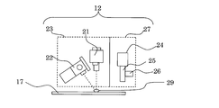
- FIG. 2 is a schematic view of the main part of the inspection apparatus 10 according to the embodiment of the present invention as viewed from the side.
- the inspection head 12 includes a fluorescent X-ray analysis unit 23 and a camera unit 27.
- the X-ray fluorescence analysis unit cannot be aligned at a certain position.
- a color filter with a side of several meters can be moved to an arbitrary position on the entire surface, and can be aligned with a foreign substance with a size of several tens to several ⁇ m. It is actually difficult to perform analysis by the unit 23.
- the inspection apparatus 10 of the present embodiment is provided with a camera unit 27 having a CCD camera 24, a lens 25, and an illumination 26, which are imaging means, in the inspection head 12, so that the foreign matter 29 to be inspected on the color filter 17 is located.
- a camera unit 27 having a CCD camera 24, a lens 25, and an illumination 26, which are imaging means, in the inspection head 12, so that the foreign matter 29 to be inspected on the color filter 17 is located.
- an image in the vicinity of the place where the foreign material 29 is present is acquired, and this image is processed to extract a foreign material defect, and the coordinates of the foreign material 29 are determined in detail from the current position of the camera unit 27 and the foreign material position in the image.
- the inspection head 12 does not need to include the camera unit 27.
- the camera unit 27 can be fixed to the fluorescent X-ray analysis unit 23 and moved integrally as shown in FIG. 2, or can be moved separately from the fluorescent X-ray analysis unit 23. It is good also as a various form.
- the fluorescent X-ray analysis unit 23 moves to the coordinates of the foreign matter 29 determined in detail by the camera unit 27. More specifically, the fluorescent X-ray analysis unit 23 moves to a position where the X-ray source 22 of the X-ray fluorescence analysis unit 23 can irradiate X-rays with short wavelengths and high energy onto the coordinates of the foreign matter 29. Since the X-ray irradiated foreign matter 29 generates fluorescent X-rays peculiar to the elements contained in the foreign matter 29, the X-ray detector 21 measures the fluorescent X-rays.
- the X-ray detector 21 sends information on the measured wavelength and intensity of the fluorescent X-rays to the analysis means 14.
- the analysis means 14 analyzes the type and content of the elements contained in the foreign matter 29 from the information and sends them to the determination means 15.
- a comparison is made with a preset threshold value according to the type of the detected metal element. If even one of the metal element types exceeds the threshold value, the foreign matter of the color filter is made conductive. And the color filter is determined to be defective.
- the metal element to be detected since the material of the conductive foreign material is generally iron or aluminum, the metal element to be detected may be limited to the Fe element or Al element. In this case, the detection efficiency can be improved as compared with the case where all metal elements are detected.
- the content of these metal elements can be adopted as the threshold value, a numerical value related to the content of the metal element can also be adopted.
- the value of the fluorescent X-ray intensity specific to the metal element may be used as the threshold value.
- the intensity of fluorescent X-rays peculiar to Fe elements or the intensity of fluorescent X-rays peculiar to Al elements is measured, and compared with a preset threshold value, if the measured value exceeds the threshold value, the foreign matter is removed.
- the color filter is determined to be defective by estimating the conductivity. And when it determines with a defect, it is desirable to call attention with various displays, such as a screen of the display apparatus attached to the control means 16, an alarm lamp, an alarm sound, etc.
- the X-ray source 22 the X-ray detector 21, and the analyzing means 14, those commercially available as fluorescent X-ray analyzers can be used.
- the color filter 17 has a color filter film formed on a glass plate.
- a colored film of red (R), green (G), and blue (B) corresponds to each pixel. It is arranged.
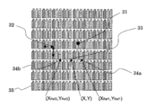
- FIG. 3 shows a schematic diagram of an example of an image 35 when such a color filter 17 is captured by the camera unit 27.
- FIG. 4 schematically shows the brightness difference D ′ (X, Y) obtained by the image processing calculation according to the formula [1] as the post-processing image 42.
- the region 43 at the left and right end portions of the processed image 42 becomes an invalid region because the comparison point cannot be set and the processing calculation according to the equation 1 cannot be performed.
- the processing calculation by the formula [1] was possible, only the coordinates of the foreign matter 31 have a value of D ′ (X, Y) having a large absolute value. Coordinates can be determined.
- the detailed coordinate measuring method of the foreign matter 31 described above is applicable when the camera unit 27 can capture a relatively wide area.
- a detailed coordinate measuring method of the foreign material 31 when the camera unit 27 cannot capture a very large area will be described with reference to FIGS. 5 and 6.
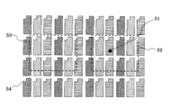
- the camera unit 27 moves to a position away from the defect position on the color filter 54 by a separately input comparison pitch, and acquires the reference image 53. . Next, it moves to the defect position and acquires an image 52 near the position where the defect 51 is supposed to be included. An image 62 obtained by differential processing between the two images is obtained, and the foreign object defect 51 is extracted. From the current position of the camera unit 27 and the foreign object defect position in the processed image 62, the coordinates of the foreign object 51 can be determined in detail.
- the camera unit 27 moves to a position separated from the defect position on the color filter 74 by a separately input comparison pitch, and acquires a reference image 73. . Next, it moves to the defect position and acquires an image 72 near the position where the defect 71 is supposed to be included.
- the amount of misregistration in both images is calculated by performing a pattern matching process on the two images using the pattern of the color filter 74. Subsequently, after the reference image is shifted by the calculated amount of displacement, an image 82 obtained by differential processing of both images is obtained, and the defect 71 is extracted. From the current position of the camera unit 27 and the position of the foreign object defect in the processed image 82, the coordinates of the foreign object 71 can be determined in detail.
- the foreign matter can be accurately irradiated with X-rays, so that precise and efficient fluorescent X-ray analysis is possible. Is possible. For this reason, it becomes possible to inspect efficiently and quickly by using it in the substrate manufacturing process.
- the X-ray source is driven under the conditions of a tube voltage of 100 kV and a tube current of 100 mA, and the inspection is performed with a measurement time of 10 seconds, the diameter is about 10 ⁇ m.
- An output of 15,000 cps was obtained for the Fe particles at an energy of Fe—K ⁇ rays (cps is a unit representing the number of X-ray photons measured per second).
- the output was 200 cps for a resin sphere having a diameter of about 50 ⁇ m.
- the output was 180 cps at a position where no defect existed on the color filter. Therefore, Fe particles having a diameter of about 10 ⁇ m can be detected and determined by setting the threshold to 1,000 cps in the determination means.
- inspection apparatus which is embodiment of this invention.
- inspection apparatus which is embodiment of this invention from the side surface.
Landscapes
- General Health & Medical Sciences (AREA)
- Life Sciences & Earth Sciences (AREA)
- Chemical & Material Sciences (AREA)
- Analytical Chemistry (AREA)
- Biochemistry (AREA)
- Immunology (AREA)
- Physics & Mathematics (AREA)
- Health & Medical Sciences (AREA)
- Pathology (AREA)
- General Physics & Mathematics (AREA)
- Liquid Crystal (AREA)
- Investigating Materials By The Use Of Optical Means Adapted For Particular Applications (AREA)
- Analysing Materials By The Use Of Radiation (AREA)
- Optical Filters (AREA)
Abstract
La présente invention concerne un procédé et un appareil de recherche de corps étrangers adhérant à un substrat pour afficheur à cristaux liquides, en se basant sur les dimensions et la conductivité. À cet effet, l'invention propose un procédé de recherche de la présence de corps étrangers contenant un élément métallique et adhérant à un substrat pour appareil à écran à cristaux liquides. Le procédé est caractérisé en ce qu'il comporte une première étape d'examen consistant à établir les dimensions et l'emplacement du corps étranger adhérant au substrat, et une seconde étape d'examen consistant à établir si le corps étranger contient un élément métallique, et ce, par alignement sur la position détectée dans la première étape d'examen.
Priority Applications (3)
| Application Number | Priority Date | Filing Date | Title |
|---|---|---|---|
| JP2008531053A JP4404159B2 (ja) | 2008-01-21 | 2008-02-15 | 検査方法 |
| US12/625,174 US7852982B2 (en) | 2008-01-21 | 2009-11-24 | Test method |
| US12/939,382 US8358735B2 (en) | 2008-01-21 | 2010-11-04 | Test method and test device |
Applications Claiming Priority (2)
| Application Number | Priority Date | Filing Date | Title |
|---|---|---|---|
| JP2008-010300 | 2008-01-21 | ||
| JP2008010300 | 2008-01-21 |
Related Child Applications (1)
| Application Number | Title | Priority Date | Filing Date |
|---|---|---|---|
| US12/625,174 Continuation US7852982B2 (en) | 2008-01-21 | 2009-11-24 | Test method |
Publications (1)
| Publication Number | Publication Date |
|---|---|
| WO2009093341A1 true WO2009093341A1 (fr) | 2009-07-30 |
Family
ID=40900859
Family Applications (1)
| Application Number | Title | Priority Date | Filing Date |
|---|---|---|---|
| PCT/JP2008/052560 Ceased WO2009093341A1 (fr) | 2008-01-21 | 2008-02-15 | Procédé et appareil de recherche |
Country Status (3)
| Country | Link |
|---|---|
| US (2) | US7852982B2 (fr) |
| JP (3) | JP4404159B2 (fr) |
| WO (1) | WO2009093341A1 (fr) |
Cited By (3)
| Publication number | Priority date | Publication date | Assignee | Title |
|---|---|---|---|---|
| JP2011169821A (ja) * | 2010-02-19 | 2011-09-01 | Sii Nanotechnology Inc | X線分析装置およびx線分析のマッピング方法 |
| JP2011232204A (ja) * | 2010-04-28 | 2011-11-17 | Rigaku Corp | カラーフィルタ基板検査方法及び検査装置 |
| WO2020066161A1 (fr) * | 2018-09-28 | 2020-04-02 | 株式会社リガク | Dispositif de mesure, programme et procédé de commande de dispositif de mesure |
Families Citing this family (18)
| Publication number | Priority date | Publication date | Assignee | Title |
|---|---|---|---|---|
| US8502967B2 (en) * | 2011-02-01 | 2013-08-06 | Cooper S. K. Kuo | Apparatus for optical inspection |
| JP5684612B2 (ja) * | 2011-03-09 | 2015-03-18 | 株式会社日立ハイテクサイエンス | X線分析装置 |
| JP5956730B2 (ja) * | 2011-08-05 | 2016-07-27 | 株式会社日立ハイテクサイエンス | X線分析装置及び方法 |
| JP5929106B2 (ja) * | 2011-11-07 | 2016-06-01 | 凸版印刷株式会社 | 検査方法および検査装置 |
| US20130215419A1 (en) * | 2012-02-22 | 2013-08-22 | Cooper S. K. Kuo | Optical inspection device |
| CN102621149B (zh) * | 2012-03-21 | 2015-07-22 | 深圳市华星光电技术有限公司 | 基板的检测装置及方法 |
| JP2014048182A (ja) * | 2012-08-31 | 2014-03-17 | Sharp Corp | 膜厚測定装置 |
| JP5919146B2 (ja) * | 2012-09-04 | 2016-05-18 | シャープ株式会社 | 膜厚測定装置 |
| JP2014048275A (ja) * | 2012-09-04 | 2014-03-17 | Sharp Corp | オフセット量校正試料および膜厚測定装置 |
| JP2014052312A (ja) * | 2012-09-07 | 2014-03-20 | Sharp Corp | 膜厚測定装置 |
| JP2014052291A (ja) * | 2012-09-07 | 2014-03-20 | Sharp Corp | ゲイン校正試料、膜厚測定装置およびゲイン校正方法 |
| JP2014055802A (ja) * | 2012-09-11 | 2014-03-27 | Sharp Corp | 膜厚測定装置および膜厚測定方法 |
| KR20140101612A (ko) * | 2013-02-12 | 2014-08-20 | 삼성디스플레이 주식회사 | 결정화 검사장치 및 결정화 검사방법 |
| US10571413B2 (en) * | 2015-04-15 | 2020-02-25 | Yxlon International Gmbh | Method for checking an electronic component |
| SG11202103927WA (en) * | 2018-10-18 | 2021-05-28 | Security Matters Ltd | System and method for detection and identification of foreign elements in a substance |
| FR3111703B1 (fr) * | 2020-06-18 | 2022-05-20 | Skf Svenska Kullagerfab Ab | Procédé de détection d’un défaut critique pour élément roulant en matériau céramique |
| US12442746B2 (en) * | 2023-02-28 | 2025-10-14 | Toyota Research Institute, Inc. | Foreign metallic particle detector systems and methods of detecting foreign metallic particles |
| US12590878B2 (en) * | 2023-02-28 | 2026-03-31 | Toyota Research Institute, Inc. | Systems and methods for detecting foreign metallic particles |
Citations (7)
| Publication number | Priority date | Publication date | Assignee | Title |
|---|---|---|---|---|
| JPH07119717B2 (ja) * | 1989-12-12 | 1995-12-20 | シャープ株式会社 | 半導体材料評価装置 |
| JPH0875683A (ja) * | 1994-07-06 | 1996-03-22 | Rigaku Ind Co | 蛍光x線分析装置 |
| JPH08145901A (ja) * | 1994-11-21 | 1996-06-07 | Hitachi Electron Eng Co Ltd | 透明金属薄膜基板の異物検査装置 |
| JPH11316201A (ja) * | 1998-01-30 | 1999-11-16 | Rigaku Industrial Co | 試料表面の検査方法およびこれを使用するx線分析装置 |
| JP2000009661A (ja) * | 1998-06-26 | 2000-01-14 | Ntn Corp | フラットパネル検査装置 |
| JP2002257756A (ja) * | 2001-03-02 | 2002-09-11 | Nippon Sheet Glass Co Ltd | ガラス製品の製造方法及び製造装置 |
| JP2004170092A (ja) * | 2002-11-18 | 2004-06-17 | Hitachi Electronics Eng Co Ltd | 表面検査方法及び表面検査装置 |
Family Cites Families (15)
| Publication number | Priority date | Publication date | Assignee | Title |
|---|---|---|---|---|
| US5461654A (en) * | 1992-04-07 | 1995-10-24 | Grodzins; Lee | X-ray fluorescence detector |
| JP3258821B2 (ja) * | 1994-06-02 | 2002-02-18 | 三菱電機株式会社 | 微小異物の位置決め方法、分析方法、これに用いる分析装置およびこれを用いた半導体素子もしくは液晶表示素子の製法 |
| JPH08145849A (ja) * | 1994-11-22 | 1996-06-07 | Yokogawa Electric Corp | カラーフィルタ検査装置 |
| JP2813147B2 (ja) * | 1995-02-14 | 1998-10-22 | 三菱電機株式会社 | 微小異物の分析方法、分析装置およびこれらを用いる半導体素子もしくは液晶表示素子の製法 |
| JPH11132720A (ja) * | 1997-10-30 | 1999-05-21 | Matsushita Electric Ind Co Ltd | 点欠陥検出装置及び方法 |
| JP2001196429A (ja) * | 2000-01-06 | 2001-07-19 | Mitsubishi Electric Corp | 歩留まり管理システムおよびその対象物とされた装置 |
| JP2002082217A (ja) * | 2000-06-28 | 2002-03-22 | Dainippon Printing Co Ltd | カラーフィルタ異物除去方法 |
| US20030068829A1 (en) * | 2001-06-25 | 2003-04-10 | Symyx Technologies, Inc. | High throughput crystallographic screening of materials |
| JP2003149183A (ja) * | 2001-11-09 | 2003-05-21 | Nippon Light Metal Co Ltd | Al−Fe系化合物のEPMA同定法 |
| JP2004117062A (ja) * | 2002-09-24 | 2004-04-15 | Seiko Epson Corp | 電気光学パネル用基板の検査方法、電気光学パネル用基板の製造方法、電気光学パネル用基板、電気光学装置および電子機器 |
| JP2005055265A (ja) * | 2003-08-01 | 2005-03-03 | Hitachi High-Tech Electronics Engineering Co Ltd | X線分析装置、x線分析方法、及び表面検査装置 |
| JP2005181015A (ja) * | 2003-12-17 | 2005-07-07 | Toppan Printing Co Ltd | カラーフィルタの検査方法及び検査装置 |
| JP2006189281A (ja) * | 2005-01-05 | 2006-07-20 | Hitachi High-Technologies Corp | 表面検査装置及び表面検査方法 |
| JP2006208137A (ja) * | 2005-01-27 | 2006-08-10 | Seiko Epson Corp | マトリクス構造の欠陥検出方法およびマトリクス構造の欠陥検出装置 |
| US7245695B2 (en) * | 2005-04-11 | 2007-07-17 | Jordan Valley Applied Radiation Ltd. | Detection of dishing and tilting using X-ray fluorescence |
-
2008
- 2008-02-15 WO PCT/JP2008/052560 patent/WO2009093341A1/fr not_active Ceased
- 2008-02-15 JP JP2008531053A patent/JP4404159B2/ja not_active Expired - Fee Related
- 2008-09-18 JP JP2008239206A patent/JP5272604B2/ja not_active Expired - Fee Related
-
2009
- 2009-06-12 JP JP2009140922A patent/JP5272909B2/ja not_active Expired - Fee Related
- 2009-11-24 US US12/625,174 patent/US7852982B2/en not_active Expired - Fee Related
-
2010
- 2010-11-04 US US12/939,382 patent/US8358735B2/en not_active Expired - Fee Related
Patent Citations (7)
| Publication number | Priority date | Publication date | Assignee | Title |
|---|---|---|---|---|
| JPH07119717B2 (ja) * | 1989-12-12 | 1995-12-20 | シャープ株式会社 | 半導体材料評価装置 |
| JPH0875683A (ja) * | 1994-07-06 | 1996-03-22 | Rigaku Ind Co | 蛍光x線分析装置 |
| JPH08145901A (ja) * | 1994-11-21 | 1996-06-07 | Hitachi Electron Eng Co Ltd | 透明金属薄膜基板の異物検査装置 |
| JPH11316201A (ja) * | 1998-01-30 | 1999-11-16 | Rigaku Industrial Co | 試料表面の検査方法およびこれを使用するx線分析装置 |
| JP2000009661A (ja) * | 1998-06-26 | 2000-01-14 | Ntn Corp | フラットパネル検査装置 |
| JP2002257756A (ja) * | 2001-03-02 | 2002-09-11 | Nippon Sheet Glass Co Ltd | ガラス製品の製造方法及び製造装置 |
| JP2004170092A (ja) * | 2002-11-18 | 2004-06-17 | Hitachi Electronics Eng Co Ltd | 表面検査方法及び表面検査装置 |
Cited By (8)
| Publication number | Priority date | Publication date | Assignee | Title |
|---|---|---|---|---|
| JP2011169821A (ja) * | 2010-02-19 | 2011-09-01 | Sii Nanotechnology Inc | X線分析装置およびx線分析のマッピング方法 |
| JP2011232204A (ja) * | 2010-04-28 | 2011-11-17 | Rigaku Corp | カラーフィルタ基板検査方法及び検査装置 |
| WO2020066161A1 (fr) * | 2018-09-28 | 2020-04-02 | 株式会社リガク | Dispositif de mesure, programme et procédé de commande de dispositif de mesure |
| KR20200136037A (ko) * | 2018-09-28 | 2020-12-04 | 가부시키가이샤 리가쿠 | 측정 장치, 프로그램 및 측정 장치의 제어 방법 |
| CN112204387A (zh) * | 2018-09-28 | 2021-01-08 | 株式会社理学 | 测量装置、程序及测量装置的控制方法 |
| KR102238799B1 (ko) | 2018-09-28 | 2021-04-09 | 가부시키가이샤 리가쿠 | 측정 장치, 프로그램 및 측정 장치의 제어 방법 |
| US11125704B2 (en) | 2018-09-28 | 2021-09-21 | Rigaku Corporation | Measurement system, program, and measurement system control method |
| CN112204387B (zh) * | 2018-09-28 | 2022-03-15 | 株式会社理学 | 测量装置、计算机可读存储介质及测量装置的控制方法 |
Also Published As
| Publication number | Publication date |
|---|---|
| JP5272909B2 (ja) | 2013-08-28 |
| JP5272604B2 (ja) | 2013-08-28 |
| JP2009198485A (ja) | 2009-09-03 |
| US20100074405A1 (en) | 2010-03-25 |
| JP4404159B2 (ja) | 2010-01-27 |
| JPWO2009093341A1 (ja) | 2011-05-26 |
| JP2009258114A (ja) | 2009-11-05 |
| US8358735B2 (en) | 2013-01-22 |
| US7852982B2 (en) | 2010-12-14 |
| US20110080998A1 (en) | 2011-04-07 |
Similar Documents
| Publication | Publication Date | Title |
|---|---|---|
| JP4404159B2 (ja) | 検査方法 | |
| CN1954204B (zh) | 使用按需自动光学检查子系统的改进的tft液晶显示器面板检查方法 | |
| EP2482059B1 (fr) | Appareil pour l'inspection optique | |
| WO2008068894A1 (fr) | Dispositif et procédé de détection de défauts, dispositif, procédé et programme de traitement d'informations | |
| WO2010024082A1 (fr) | Système d’inspection des défauts et procédé d’inspection des défauts | |
| CN110208269B (zh) | 一种玻璃表面异物与内部异物区分的方法及系统 | |
| US20120044346A1 (en) | Apparatus and method for inspecting internal defect of substrate | |
| CN1573482A (zh) | 检查和修补液晶显示器件的方法和装置 | |
| WO2012153662A1 (fr) | Procédé et dispositif d'inspection de très petits défauts sur corps en forme de plaque translucide | |
| JP5929106B2 (ja) | 検査方法および検査装置 | |
| JP4909691B2 (ja) | 電子部品の実装状態検査方法、電子部品の実装状態検査装置及び電子機器の製造方法 | |
| JP2017015564A (ja) | 薄膜フィルム用検査装置 | |
| CN106030285B (zh) | 用于测试石墨烯传导性的装置和方法 | |
| CN102297874A (zh) | 滤色片基板检查方法及检查装置 | |
| TWI391650B (zh) | 基板品質測試器 | |
| KR20140012485A (ko) | 평판 검사 방법 및 장치 | |
| JP2012088139A (ja) | 塗工膜の欠陥検査装置及び検査方法 | |
| JP2007093330A (ja) | 欠陥抽出装置及び欠陥抽出方法 | |
| KR102063680B1 (ko) | 표시 패널의 검사 장치 및 검사 방법 | |
| TWM457889U (zh) | 面板瑕疵檢測之裝置 | |
| JP2003177371A (ja) | 液晶表示装置の検査装置及びその検査方法 | |
| JP4009595B2 (ja) | パターン欠陥検査装置およびパターン欠陥検査方法 | |
| JP2008039444A (ja) | 異物検査方法及び異物検査装置 | |
| JP2007184529A (ja) | 半導体ウエハの検査装置 | |
| WO2013035430A1 (fr) | Dispositif et procédé de contrôle des défauts pour substrat tft |
Legal Events
| Date | Code | Title | Description |
|---|---|---|---|
| WWE | Wipo information: entry into national phase |
Ref document number: 2008531053 Country of ref document: JP |
|
| 121 | Ep: the epo has been informed by wipo that ep was designated in this application |
Ref document number: 08711390 Country of ref document: EP Kind code of ref document: A1 |
|
| NENP | Non-entry into the national phase |
Ref country code: DE |
|
| 122 | Ep: pct application non-entry in european phase |
Ref document number: 08711390 Country of ref document: EP Kind code of ref document: A1 |