WO2009093376A1 - Procédé de fabrication d'un élément d'onde élastique - Google Patents
Procédé de fabrication d'un élément d'onde élastique Download PDFInfo
- Publication number
- WO2009093376A1 WO2009093376A1 PCT/JP2008/071415 JP2008071415W WO2009093376A1 WO 2009093376 A1 WO2009093376 A1 WO 2009093376A1 JP 2008071415 W JP2008071415 W JP 2008071415W WO 2009093376 A1 WO2009093376 A1 WO 2009093376A1
- Authority
- WO
- WIPO (PCT)
- Prior art keywords
- substrate
- piezoelectric substrate
- idt
- acoustic wave
- main surface
- Prior art date
- Legal status (The legal status is an assumption and is not a legal conclusion. Google has not performed a legal analysis and makes no representation as to the accuracy of the status listed.)
- Ceased
Links
Images



Classifications
-
- H—ELECTRICITY
- H03—ELECTRONIC CIRCUITRY
- H03H—IMPEDANCE NETWORKS, e.g. RESONANT CIRCUITS; RESONATORS
- H03H3/00—Apparatus or processes specially adapted for the manufacture of impedance networks, resonating circuits, resonators
- H03H3/007—Apparatus or processes specially adapted for the manufacture of impedance networks, resonating circuits, resonators for the manufacture of electromechanical resonators or networks
- H03H3/02—Apparatus or processes specially adapted for the manufacture of impedance networks, resonating circuits, resonators for the manufacture of electromechanical resonators or networks for the manufacture of piezoelectric or electrostrictive resonators or networks
-
- C—CHEMISTRY; METALLURGY
- C23—COATING METALLIC MATERIAL; COATING MATERIAL WITH METALLIC MATERIAL; CHEMICAL SURFACE TREATMENT; DIFFUSION TREATMENT OF METALLIC MATERIAL; COATING BY VACUUM EVAPORATION, BY SPUTTERING, BY ION IMPLANTATION OR BY CHEMICAL VAPOUR DEPOSITION, IN GENERAL; INHIBITING CORROSION OF METALLIC MATERIAL OR INCRUSTATION IN GENERAL
- C23C—COATING METALLIC MATERIAL; COATING MATERIAL WITH METALLIC MATERIAL; SURFACE TREATMENT OF METALLIC MATERIAL BY DIFFUSION INTO THE SURFACE, BY CHEMICAL CONVERSION OR SUBSTITUTION; COATING BY VACUUM EVAPORATION, BY SPUTTERING, BY ION IMPLANTATION OR BY CHEMICAL VAPOUR DEPOSITION, IN GENERAL
- C23C4/00—Coating by spraying the coating material in the molten state, e.g. by flame, plasma or electric discharge
- C23C4/04—Coating by spraying the coating material in the molten state, e.g. by flame, plasma or electric discharge characterised by the coating material
- C23C4/06—Metallic material
-
- H—ELECTRICITY
- H03—ELECTRONIC CIRCUITRY
- H03H—IMPEDANCE NETWORKS, e.g. RESONANT CIRCUITS; RESONATORS
- H03H3/00—Apparatus or processes specially adapted for the manufacture of impedance networks, resonating circuits, resonators
- H03H3/007—Apparatus or processes specially adapted for the manufacture of impedance networks, resonating circuits, resonators for the manufacture of electromechanical resonators or networks
-
- H—ELECTRICITY
- H03—ELECTRONIC CIRCUITRY
- H03H—IMPEDANCE NETWORKS, e.g. RESONANT CIRCUITS; RESONATORS
- H03H3/00—Apparatus or processes specially adapted for the manufacture of impedance networks, resonating circuits, resonators
- H03H3/007—Apparatus or processes specially adapted for the manufacture of impedance networks, resonating circuits, resonators for the manufacture of electromechanical resonators or networks
- H03H3/02—Apparatus or processes specially adapted for the manufacture of impedance networks, resonating circuits, resonators for the manufacture of electromechanical resonators or networks for the manufacture of piezoelectric or electrostrictive resonators or networks
- H03H3/04—Apparatus or processes specially adapted for the manufacture of impedance networks, resonating circuits, resonators for the manufacture of electromechanical resonators or networks for the manufacture of piezoelectric or electrostrictive resonators or networks for obtaining desired frequency or temperature coefficient
-
- H—ELECTRICITY
- H03—ELECTRONIC CIRCUITRY
- H03H—IMPEDANCE NETWORKS, e.g. RESONANT CIRCUITS; RESONATORS
- H03H3/00—Apparatus or processes specially adapted for the manufacture of impedance networks, resonating circuits, resonators
- H03H3/007—Apparatus or processes specially adapted for the manufacture of impedance networks, resonating circuits, resonators for the manufacture of electromechanical resonators or networks
- H03H3/08—Apparatus or processes specially adapted for the manufacture of impedance networks, resonating circuits, resonators for the manufacture of electromechanical resonators or networks for the manufacture of resonators or networks using surface acoustic waves
- H03H3/10—Apparatus or processes specially adapted for the manufacture of impedance networks, resonating circuits, resonators for the manufacture of electromechanical resonators or networks for the manufacture of resonators or networks using surface acoustic waves for obtaining desired frequency or temperature coefficient
-
- H—ELECTRICITY
- H03—ELECTRONIC CIRCUITRY
- H03H—IMPEDANCE NETWORKS, e.g. RESONANT CIRCUITS; RESONATORS
- H03H9/00—Networks comprising electromechanical or electro-acoustic elements; Electromechanical resonators
- H03H9/02—Details
- H03H9/02535—Details of surface acoustic wave devices
- H03H9/02543—Characteristics of substrate, e.g. cutting angles
- H03H9/02559—Characteristics of substrate, e.g. cutting angles of lithium niobate or lithium-tantalate substrates
-
- C—CHEMISTRY; METALLURGY
- C23—COATING METALLIC MATERIAL; COATING MATERIAL WITH METALLIC MATERIAL; CHEMICAL SURFACE TREATMENT; DIFFUSION TREATMENT OF METALLIC MATERIAL; COATING BY VACUUM EVAPORATION, BY SPUTTERING, BY ION IMPLANTATION OR BY CHEMICAL VAPOUR DEPOSITION, IN GENERAL; INHIBITING CORROSION OF METALLIC MATERIAL OR INCRUSTATION IN GENERAL
- C23C—COATING METALLIC MATERIAL; COATING MATERIAL WITH METALLIC MATERIAL; SURFACE TREATMENT OF METALLIC MATERIAL BY DIFFUSION INTO THE SURFACE, BY CHEMICAL CONVERSION OR SUBSTITUTION; COATING BY VACUUM EVAPORATION, BY SPUTTERING, BY ION IMPLANTATION OR BY CHEMICAL VAPOUR DEPOSITION, IN GENERAL
- C23C4/00—Coating by spraying the coating material in the molten state, e.g. by flame, plasma or electric discharge
- C23C4/04—Coating by spraying the coating material in the molten state, e.g. by flame, plasma or electric discharge characterised by the coating material
-
- C—CHEMISTRY; METALLURGY
- C23—COATING METALLIC MATERIAL; COATING MATERIAL WITH METALLIC MATERIAL; CHEMICAL SURFACE TREATMENT; DIFFUSION TREATMENT OF METALLIC MATERIAL; COATING BY VACUUM EVAPORATION, BY SPUTTERING, BY ION IMPLANTATION OR BY CHEMICAL VAPOUR DEPOSITION, IN GENERAL; INHIBITING CORROSION OF METALLIC MATERIAL OR INCRUSTATION IN GENERAL
- C23C—COATING METALLIC MATERIAL; COATING MATERIAL WITH METALLIC MATERIAL; SURFACE TREATMENT OF METALLIC MATERIAL BY DIFFUSION INTO THE SURFACE, BY CHEMICAL CONVERSION OR SUBSTITUTION; COATING BY VACUUM EVAPORATION, BY SPUTTERING, BY ION IMPLANTATION OR BY CHEMICAL VAPOUR DEPOSITION, IN GENERAL
- C23C4/00—Coating by spraying the coating material in the molten state, e.g. by flame, plasma or electric discharge
- C23C4/04—Coating by spraying the coating material in the molten state, e.g. by flame, plasma or electric discharge characterised by the coating material
- C23C4/10—Oxides, borides, carbides, nitrides or silicides; Mixtures thereof
-
- Y—GENERAL TAGGING OF NEW TECHNOLOGICAL DEVELOPMENTS; GENERAL TAGGING OF CROSS-SECTIONAL TECHNOLOGIES SPANNING OVER SEVERAL SECTIONS OF THE IPC; TECHNICAL SUBJECTS COVERED BY FORMER USPC CROSS-REFERENCE ART COLLECTIONS [XRACs] AND DIGESTS
- Y10—TECHNICAL SUBJECTS COVERED BY FORMER USPC
- Y10T—TECHNICAL SUBJECTS COVERED BY FORMER US CLASSIFICATION
- Y10T29/00—Metal working
- Y10T29/42—Piezoelectric device making
-
- Y—GENERAL TAGGING OF NEW TECHNOLOGICAL DEVELOPMENTS; GENERAL TAGGING OF CROSS-SECTIONAL TECHNOLOGIES SPANNING OVER SEVERAL SECTIONS OF THE IPC; TECHNICAL SUBJECTS COVERED BY FORMER USPC CROSS-REFERENCE ART COLLECTIONS [XRACs] AND DIGESTS
- Y10—TECHNICAL SUBJECTS COVERED BY FORMER USPC
- Y10T—TECHNICAL SUBJECTS COVERED BY FORMER US CLASSIFICATION
- Y10T29/00—Metal working
- Y10T29/49—Method of mechanical manufacture
- Y10T29/49002—Electrical device making
- Y10T29/49117—Conductor or circuit manufacturing
- Y10T29/49124—On flat or curved insulated base, e.g., printed circuit, etc.
- Y10T29/49147—Assembling terminal to base
-
- Y—GENERAL TAGGING OF NEW TECHNOLOGICAL DEVELOPMENTS; GENERAL TAGGING OF CROSS-SECTIONAL TECHNOLOGIES SPANNING OVER SEVERAL SECTIONS OF THE IPC; TECHNICAL SUBJECTS COVERED BY FORMER USPC CROSS-REFERENCE ART COLLECTIONS [XRACs] AND DIGESTS
- Y10—TECHNICAL SUBJECTS COVERED BY FORMER USPC
- Y10T—TECHNICAL SUBJECTS COVERED BY FORMER US CLASSIFICATION
- Y10T29/00—Metal working
- Y10T29/49—Method of mechanical manufacture
- Y10T29/49002—Electrical device making
- Y10T29/49117—Conductor or circuit manufacturing
- Y10T29/49124—On flat or curved insulated base, e.g., printed circuit, etc.
- Y10T29/49155—Manufacturing circuit on or in base
Definitions
- the present invention relates to a method for manufacturing an acoustic wave device such as a surface acoustic wave (SAW) device or a boundary acoustic wave device.
- SAW surface acoustic wave
- An acoustic wave element is an element formed by forming a comb-type electrode (Inter-Digital Transducer: IDT) on a piezoelectric substrate such as a lithium tantalate (LiTaO 3 : LT) substrate or a lithium niobate (LiNbO 3 : LN) substrate. is there.
- the thermal expansion coefficient of LT and LN is about 6 times that of silicon (LT is about 16 ⁇ 10 ⁇ 6 / K, LN is about 15 ⁇ 10 ⁇ 6 / K compared to about 2.6 ⁇ 10 ⁇ 6 / K for silicon). Therefore, when an LT substrate or an LN substrate is used for an acoustic wave element, a change in filter characteristics due to a temperature change becomes a serious problem. For this reason, temperature compensation is performed by various methods.
- Patent Document 1 discloses a technique in which a thinned piezoelectric substrate and a temperature-compensating amorphous piezoelectric substrate are bonded directly or via an inorganic thin film layer.
- Patent Document 2 discloses that a piezoelectric substrate thinned after forming an IDT and an insulating substrate for temperature compensation are joined by an adhesive member made of a vitreous body. JP-A-6-326553 Japanese Patent Laid-Open No. 2002-16468
- a bonded substrate formed by bonding a piezoelectric substrate and a temperature compensation substrate is used for a wafer process, for example, when an IDT for an acoustic wave element is formed on a bonded substrate, the piezoelectric substrate and temperature characteristic compensation are performed by a heating process in the process. Stress due to a difference in linear expansion coefficient between the substrate and the piezoelectric substrate is warped, and accordingly, the line width processing accuracy is lowered. Also, in the wafer process, processing at a temperature of 200 ° C. or higher may be performed. When the bonded substrate is subjected to such a temperature, stress due to a difference in linear expansion coefficient is generated, and the substrate is cracked or bonded. Peeling may occur.
- the present invention has been made in view of the above points, and is an elastic wave element that is excellent in frequency temperature characteristics (TCF: Temperature Coefficient of Frequency), has high IDT pattern processing accuracy, and can withstand high-temperature processing at 200 ° C. or higher.
- TCF Temperature Coefficient of Frequency
- the method for manufacturing an acoustic wave device of the present invention includes a step of forming an IDT on one main surface of a piezoelectric substrate, and a linear expansion coefficient of the piezoelectric substrate on the other main surface of the piezoelectric substrate after the IDT is formed. And a step of depositing a material having a smaller linear expansion coefficient by thermal spraying.
- the sprayed film exhibiting the temperature compensation effect is formed.
- the IDT since the IDT is formed on the piezoelectric substrate, the warpage of the substrate due to the generation of stress caused by the difference in linear expansion coefficient, and the substrate cracking in the high temperature process, which are problems in the bonded substrate, do not occur. Since the IDT can be formed without warping of the substrate, an acoustic wave element with high IDT processing accuracy can be obtained. Furthermore, after forming the IDT, since the thermal spray film that exhibits the temperature compensation effect is formed, the acoustic wave device obtained thereby exhibits the temperature compensation effect even when the IDT processing accuracy is high. Can do.
- an acoustic wave device of the present invention it is preferable to further include a step of thinning the other main surface of the piezoelectric substrate before film formation by thermal spraying. According to this method, an acoustic wave device having a higher temperature compensation effect can be obtained.
- the material is preferably at least one selected from the group consisting of mullite, alumina, silicon, and yttria.
- the piezoelectric substrate is preferably a lithium tantalate substrate or a lithium niobate substrate.
- the method for manufacturing an acoustic wave device of the present invention it is preferable that the method further includes a step of filling a hole formed in the film formed by the thermal spraying with a filler. According to this method, it is possible to increase the rigidity of the sprayed film and improve the frequency temperature characteristics.
- the IDT is formed on one main surface of the piezoelectric substrate, and the linear expansion coefficient of the piezoelectric substrate is formed on the other main surface of the piezoelectric substrate after the IDT is formed. Since a material having a smaller linear expansion coefficient is deposited by thermal spraying, it has excellent frequency temperature characteristics (TCF: TemperatureTCoefficient of Frequency), and the substrate does not warp during the process, and can be processed at a high temperature of 200 ° C or higher. An endurable elastic wave element can be obtained.
- TCF TemperatureTCoefficient of Frequency
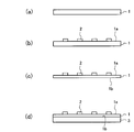
- (A)-(c) is a figure for demonstrating the manufacturing method of the elastic wave element which concerns on embodiment of this invention.
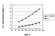
- (A)-(d) is a figure for demonstrating the other example of the manufacturing method of the elastic wave element which concerns on embodiment of this invention. It is a figure which shows the relationship between the temperature of PEB at the time of formation of IDT, and the curvature amount of a wafer. It is a figure which shows the relationship between the pattern line width processing precision R in a wafer surface, and PEB temperature.
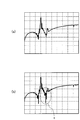
- (A), (b) is a figure which shows the influence of the bulk wave of an elastic wave element.
- an IDT is formed on one main surface of a piezoelectric substrate, and the other main surface of the piezoelectric substrate after the IDT is formed is determined from the linear expansion coefficient of the piezoelectric substrate.
- a material having a smaller linear expansion coefficient is deposited by thermal spraying.
- the acoustic wave element refers to a surface acoustic wave element and a boundary acoustic wave element.
- Examples of the piezoelectric substrate include a lithium tantalate substrate (LT substrate) and a lithium niobate substrate (LN substrate).
- LT substrate lithium tantalate substrate
- LN substrate lithium niobate substrate
- FIG. 1 is a characteristic diagram showing the relationship between the LT substrate thickness ratio (LT substrate thickness / substrate total thickness) and the temperature compensation effect.
- TCF TemperatureTCoefficient of Frequency
- FIG. 1 is a characteristic diagram showing the relationship between the LT substrate thickness ratio (LT substrate thickness / substrate total thickness) and the temperature compensation effect.
- an LT substrate is used as the piezoelectric substrate.
- the ratio of the LT substrate thickness to the total substrate thickness the higher the temperature compensation effect.
- the surfaces to be bonded are mirror-finished in order to bond the substrates together.
- the polishing process in the case of mirror-finishing is needed.
- a relatively high processing stress is applied to the substrate.
- the piezoelectric substrate may be broken due to stress in the polishing process.
- polishing is not necessary, and the piezoelectric substrate can be thinned to enhance the temperature compensation effect.
- the bulk wave of the elastic wave generated on one main surface forming the IDT is reflected on the other main surface, and this reflected wave interferes with the elastic wave generated on the one main surface.
- the back surface of the piezoelectric substrate that is, the surface on which the sprayed film is formed is preferably roughened.
- the back surface of the piezoelectric substrate is preferably a roughened surface.
- the surface roughness Ra of the back surface is preferably 0.01 ⁇ m to 3 ⁇ m.
- examples of the processing applied to the substrate surface include grinding, blasting, and lapping. Such processing is advantageous in that the stress on the substrate can be reduced as compared with the polishing processing, and the influence on the substrate is reduced.
- thermal spray film material having a linear expansion coefficient smaller than that of the piezoelectric substrate used for thermal spraying
- examples of the material (thermal spray film material) having a linear expansion coefficient smaller than that of the piezoelectric substrate used for thermal spraying include alumina, mullite, silicon, and yttria.
- the thermal spray deposition method uses electric energy (arc, plasma) or combustion energy as a heat source, and a powder or rod-shaped material of the material to be deposited is injected into this, and sprayed on the surface of the substrate as fine particles in a molten or semi-molten state, This is a method of forming a film.
- the thermal spray film formation method it is possible to suppress the thermal influence on the piezoelectric substrate during film formation as much as possible. Thereby, it becomes possible to suppress the crack and peeling resulting from the temperature rise at the time of substrate processing.
- the sprayed film is generally porous and its rigidity is relatively small. Therefore, CVD (chemical vapor deposition), PVD (physical vapor deposition), SOG (Spin On Glass) are formed in the pores. It is preferable to fill the holes by a method such as Thereby, the rigidity of the sprayed film can be increased and the frequency temperature characteristics can be improved.
- the sprayed film may be composed of a plurality of layers. By forming the sprayed film with a plurality of layers in this manner, various materials can be combined, so that the linear expansion coefficient of the sprayed film can be easily adjusted.
- a piezoelectric substrate 1 is prepared as shown in FIG. 2A, and an IDT 2 is formed on one main surface 1a as shown in FIG. 2B.
- an IDT electrode material is deposited on the main surface 1a of the piezoelectric substrate 1, a resist layer (not shown) is formed on the IDT electrode material layer (not shown), and a photomask is used.
- the resist layer in the region where the IDT is formed is exposed and developed to pattern the resist layer.
- the IDT electrode material layer is etched using the patterned resist layer as a mask, and then the remaining resist layer is removed.
- the other main surface (back surface) 1b of the piezoelectric substrate 1 is made of a material having a linear expansion coefficient smaller than the linear expansion coefficient of the piezoelectric substrate 1 by a thermal spray film forming method.
- the sprayed film 3 is formed. If necessary, the sprayed film is impregnated with SOG and cured to improve the rigidity of the sprayed film.
- the piezoelectric substrate 1 is prepared as shown in FIG. 3A, and the IDT 2 is provided on the one main surface 1a as shown in FIG. 3B.
- the piezoelectric substrate 1 is thinned from the back surface 1b side, and then, as shown in FIG. 3D, the thermal spray film forming method is formed on the back surface 1b of the piezoelectric substrate 1.
- the sprayed film 3 may be formed.
- blasting, lapping, grinding, or the like is used for thinning the piezoelectric substrate 1.
- FIG. 4 shows the relationship between the temperature of PEB (Post-Exposure-Bake) during the formation of IDT and the amount of warpage in the heated state of the wafer.
- PEB Post-Exposure-Bake
- an LT substrate is used as the piezoelectric substrate.
- core9037a trade name, manufactured by Cores.
- FIG. 4 shows the warpage amount ( ⁇ plot) of a 4-inch LT substrate alone and the warpage amount ( ⁇ plot) of a 4-inch bonded substrate (LT substrate + Si substrate).
- the LT substrate alone has a very small amount of warping compared to the bonding substrate (LT substrate + Si substrate) at a temperature equal to or lower than the temperature at which the substrate breaks.
- the pattern line width processing accuracy R within the wafer surface is increased by forming the IDT in a state where the LT substrate alone is small in the amount of warpage in the heated state. Further, at a temperature higher than the range shown in this figure, the bonded substrate is cracked and peeled off.
- FIG. 5 shows the relationship between the pattern line width processing accuracy R in the wafer surface and the PEB temperature.
- an LT substrate is used as the piezoelectric substrate.
- FIG. 5 shows the line width processing accuracy R (line width processing accuracy when patterning is directly performed on an LT substrate: ⁇ plot) and a 4-inch bonded substrate (LT substrate + Si substrate) in the wafer surface of a 4-inch LT substrate alone. ) Shows the line width processing accuracy R in the wafer surface (line width processing accuracy when pattern processing is performed on the bonded substrate: ⁇ plot).
- the IDT is formed in a single LT substrate with a small amount of warpage in the heated state, so that the line width processing accuracy is increased.
- the acoustic wave element obtained by thermal spray deposition after forming the IDT on the piezoelectric substrate forms the IDT with a small warpage of the substrate.
- the IDT processing accuracy is high.
- the influence of a bulk wave can be suppressed by roughening the sprayed surface of the piezoelectric substrate.
- the thermal spraying film forming method since there is no bonding between the substrates, it is not necessary to polish the substrate surface, and it is possible to prevent the piezoelectric substrate from being cracked due to a high processing stress at the time of thinning.
- the thermal spraying film forming method since the thermal spraying film forming method is adopted, an expensive bonding apparatus is not required, and an elastic wave element having excellent frequency temperature characteristics can be manufactured at low cost.
- Example 1 The linear expansion coefficient is 16 ⁇ 10 ⁇ 6 / K, and the linear expansion coefficient is 1 ⁇ 10 ⁇ on one main surface of a lithium tantalate substrate (LT substrate) having a thickness of 0.02 mm by a thermal spray deposition method.
- LT substrate lithium tantalate substrate
- a 6- K mullite film was formed to a thickness of 0.33 mm to produce a 4-inch substrate.
- the 4-inch substrate was subjected to heat treatment. At this time, the 4-inch substrate was not cracked at the heating temperatures of 180 ° C. and 200 ° C., but the 4-inch substrate was cracked at the heating temperatures of 250 ° C. and 350 ° C.
- a 4-inch substrate was produced in the same manner as described above using a lithium niobate substrate (LN substrate) having a linear expansion coefficient of 15 ⁇ 10 ⁇ 6 / K instead of the LT substrate and having a thickness of 0.02 mm. .
- the 4-inch substrate was subjected to heat treatment. At this time, the 4-inch substrate was not cracked at the heating temperatures of 180 ° C. and 200 ° C., but the 4-inch substrate was cracked at the heating temperatures of 250 ° C. and 350 ° C.
- the linear expansion coefficient is 3 ⁇ 10 6 on one main surface of a lithium tantalate substrate (LT substrate) having a linear expansion coefficient of 16 ⁇ 10 ⁇ 6 / K and a diameter of 4 inches and a thickness of 0.25 mm. -6 / K, a silicon substrate for temperature compensation with a diameter of 4 inches and a thickness of 0.33 mm is directly joined by the surface activation method, and then the silicon surface is thinned to a thickness of 0.02 mm by grinding and polishing.
- a layered bonded substrate was produced. Note that the surfaces to be bonded of the LT substrate and the silicon substrate were mirror-finished in advance. Next, heat treatment was performed on the bonded substrate. At this time, the LT substrate was cracked even at heating temperatures of 180 ° C. and 200 ° C.
- Example 2 An IDT was formed on one main surface of a lithium tantalate substrate (LT substrate) having a linear expansion coefficient of 16 ⁇ 10 ⁇ 6 / K, a diameter of 4 inches, and a thickness of 0.25 mm.
- LT substrate lithium tantalate substrate
- PEB Post Exposure Bake
- the other main surface of the LT substrate was thinned to a thickness of 0.01 to 0.04 mm by grinding and roughened to Ra 0.1 ⁇ m.
- silicon and alumina were sprayed in this order on the other roughened main surface by a thermal spraying method so that the total thickness of the LT substrate and the thermal sprayed film was 0.25 mm.
- the thermal spraying process was performed using a DC plasma spraying apparatus, using Ar plasma gas, with a power output of 40 kW.
- the in-plane line width processing accuracy R was examined.
- This line width processing accuracy R was measured by a length measuring SEM (Scanning Electron Microscope).
- the line width processing accuracy R in the wafer surface was about 2%. As described above, this is considered to be because the warpage of the wafer in the high-temperature processing is suppressed, and the variation in the resist line width is suppressed to be small.
- FIG. 6B shows the waveform of an acoustic wave device obtained using the bonded substrate manufactured in Example 1.
- Part X in FIG. 6B is a ripple due to the influence of bulk waves.
- the acoustic wave element obtained by the method according to the present invention did not show ripples due to bulk waves.
- the present invention is not limited to the above embodiment, and can be implemented with various modifications.
- the shape, dimensions, material, and the like in the above-described embodiment are examples, and can be appropriately changed and implemented without departing from the effects of the present invention.
- the present invention can be implemented with various modifications without departing from the scope of the present invention.
Landscapes
- Engineering & Computer Science (AREA)
- Physics & Mathematics (AREA)
- Acoustics & Sound (AREA)
- Manufacturing & Machinery (AREA)
- Chemical & Material Sciences (AREA)
- Materials Engineering (AREA)
- Plasma & Fusion (AREA)
- Chemical Kinetics & Catalysis (AREA)
- Mechanical Engineering (AREA)
- Metallurgy (AREA)
- Organic Chemistry (AREA)
- Surface Acoustic Wave Elements And Circuit Networks Thereof (AREA)
Abstract
Priority Applications (4)
| Application Number | Priority Date | Filing Date | Title |
|---|---|---|---|
| JP2009550428A JP5115562B2 (ja) | 2008-01-24 | 2008-11-26 | 弾性波素子の製造方法 |
| US12/864,060 US8997320B2 (en) | 2008-01-24 | 2008-11-26 | Method for manufacturing acoustic wave device |
| EP08871214.6A EP2246978B1 (fr) | 2008-01-24 | 2008-11-26 | Procédé de fabrication d'un élément d'onde élastique |
| CN200880125278.4A CN101971491B (zh) | 2008-01-24 | 2008-11-26 | 声波元件的制造方法 |
Applications Claiming Priority (2)
| Application Number | Priority Date | Filing Date | Title |
|---|---|---|---|
| JP2008013633 | 2008-01-24 | ||
| JP2008-013633 | 2008-01-24 |
Publications (1)
| Publication Number | Publication Date |
|---|---|
| WO2009093376A1 true WO2009093376A1 (fr) | 2009-07-30 |
Family
ID=40900891
Family Applications (1)
| Application Number | Title | Priority Date | Filing Date |
|---|---|---|---|
| PCT/JP2008/071415 Ceased WO2009093376A1 (fr) | 2008-01-24 | 2008-11-26 | Procédé de fabrication d'un élément d'onde élastique |
Country Status (5)
| Country | Link |
|---|---|
| US (1) | US8997320B2 (fr) |
| EP (1) | EP2246978B1 (fr) |
| JP (1) | JP5115562B2 (fr) |
| CN (1) | CN101971491B (fr) |
| WO (1) | WO2009093376A1 (fr) |
Cited By (4)
| Publication number | Priority date | Publication date | Assignee | Title |
|---|---|---|---|---|
| JP2011071967A (ja) * | 2009-08-24 | 2011-04-07 | Ngk Insulators Ltd | 複合基板の製造方法 |
| WO2012043615A1 (fr) * | 2010-09-28 | 2012-04-05 | 株式会社村田製作所 | Procédé de fabrication de dispositif piézoélectrique |
| WO2018159596A1 (fr) * | 2017-02-28 | 2018-09-07 | 京セラ株式会社 | Substrat pour dispositif à ondes élastiques de surface, et élément à pseudo-ondes élastiques de surface |
| US12199052B2 (en) | 2019-07-03 | 2025-01-14 | Murata Manufacturing Co., Ltd. | Radio-frequency module and communication device |
Families Citing this family (17)
| Publication number | Priority date | Publication date | Assignee | Title |
|---|---|---|---|---|
| EP2237417B1 (fr) * | 2008-01-25 | 2013-07-31 | Murata Manufacturing Co. Ltd. | Élément d'onde élastique et son procédé de fabrication |
| US9503047B2 (en) * | 2014-05-01 | 2016-11-22 | Texas Instruments Incorporated | Bulk acoustic wave (BAW) device having roughened bottom side |
| US20170063330A1 (en) * | 2015-08-25 | 2017-03-02 | Avago Technologies General Ip (Singapore) Pte. Ltd. | Surface acoustic wave (saw) resonator |
| US10090822B2 (en) | 2015-08-25 | 2018-10-02 | Avago Technologies General Ip (Singapore) Pte. Ltd. | Surface acoustic wave (SAW) resonator |
| US10536133B2 (en) | 2016-04-22 | 2020-01-14 | Avago Technologies International Sales Pte. Limited | Composite surface acoustic wave (SAW) device with absorbing layer for suppression of spurious responses |
| US10177734B2 (en) | 2015-08-25 | 2019-01-08 | Avago Technologies International Sales Pte. Limited | Surface acoustic wave (SAW) resonator |
| US10469056B2 (en) | 2015-08-25 | 2019-11-05 | Avago Technologies International Sales Pte. Limited | Acoustic filters integrated into single die |
| US10020796B2 (en) | 2015-08-25 | 2018-07-10 | Avago Technologies General Ip (Singapore) Pte. Ltd. | Surface acoustic wave (SAW) resonator |
| US9991870B2 (en) | 2015-08-25 | 2018-06-05 | Avago Technologies General Ip (Singapore) Pte. Ltd. | Surface acoustic wave (SAW) resonator |
| US10523178B2 (en) * | 2015-08-25 | 2019-12-31 | Avago Technologies International Sales Pte. Limited | Surface acoustic wave (SAW) resonator |
| US9369111B1 (en) * | 2015-10-28 | 2016-06-14 | Resonant Inc. | Fabrication of surface acoustic wave filters having plate modes |
| US10177735B2 (en) | 2016-02-29 | 2019-01-08 | Avago Technologies International Sales Pte. Limited | Surface acoustic wave (SAW) resonator |
| FR3052298B1 (fr) * | 2016-06-02 | 2018-07-13 | Soitec | Structure hybride pour dispositif a ondes acoustiques de surface |
| FR3053532B1 (fr) * | 2016-06-30 | 2018-11-16 | Soitec | Structure hybride pour dispositif a ondes acoustiques de surface |
| CN108494380A (zh) * | 2018-03-16 | 2018-09-04 | 无锡市好达电子有限公司 | 声表面波材料及其制作方法 |
| JP7336413B2 (ja) * | 2020-04-30 | 2023-08-31 | 信越化学工業株式会社 | 複合基板の製造方法および複合基板 |
| CN116054769A (zh) * | 2022-12-26 | 2023-05-02 | 泉州市三安集成电路有限公司 | 基于tc-saw键合片的滤波器制作方法 |
Citations (5)
| Publication number | Priority date | Publication date | Assignee | Title |
|---|---|---|---|---|
| JPH06326553A (ja) | 1993-03-15 | 1994-11-25 | Matsushita Electric Ind Co Ltd | 表面弾性波素子 |
| JP2002016468A (ja) | 2000-06-30 | 2002-01-18 | Kyocera Corp | 弾性表面波装置 |
| JP2002330047A (ja) | 2001-04-27 | 2002-11-15 | Kyocera Corp | 弾性表面波素子 |
| JP2005229455A (ja) * | 2004-02-16 | 2005-08-25 | Shin Etsu Chem Co Ltd | 複合圧電基板 |
| JP2008054276A (ja) * | 2006-07-27 | 2008-03-06 | Koike Co Ltd | 圧電基板及びその製造方法 |
Family Cites Families (10)
| Publication number | Priority date | Publication date | Assignee | Title |
|---|---|---|---|---|
| US4436538A (en) * | 1981-04-22 | 1984-03-13 | Nippon Soken, Inc. | Filter for cleaning exhaust gases from diesel engine |
| DE19612926C2 (de) * | 1996-04-01 | 1999-09-30 | Fraunhofer Ges Forschung | Siliciumnitrid-Kompositpulver für thermische Beschichtungstechnologien und Verfahren zu ihrer Herstellung |
| US6254938B1 (en) * | 1997-04-21 | 2001-07-03 | Ltu, Llc | Spraying method for applying a porous coating to a substrate |
| JP2001111378A (ja) * | 1999-10-13 | 2001-04-20 | Toyo Commun Equip Co Ltd | 弾性表面波素子及び弾性表面波デバイス |
| JP3780791B2 (ja) * | 2000-01-11 | 2006-05-31 | セイコーエプソン株式会社 | 表面弾性波素子 |
| TW541586B (en) * | 2001-05-25 | 2003-07-11 | Tokyo Electron Ltd | Substrate table, production method therefor and plasma treating device |
| JP2003087080A (ja) * | 2001-07-06 | 2003-03-20 | Murata Mfg Co Ltd | 弾性表面波素子及びその製造方法 |
| JP2005020547A (ja) * | 2003-06-27 | 2005-01-20 | Kyocera Corp | 弾性表面波装置 |
| DE102004045181B4 (de) * | 2004-09-17 | 2016-02-04 | Epcos Ag | SAW-Bauelement mit reduziertem Temperaturgang und Verfahren zur Herstellung |
| US7569976B2 (en) | 2006-07-27 | 2009-08-04 | Koike Co., Ltd. | Piezo-electric substrate and manufacturing method of the same |
-
2008
- 2008-11-26 WO PCT/JP2008/071415 patent/WO2009093376A1/fr not_active Ceased
- 2008-11-26 JP JP2009550428A patent/JP5115562B2/ja active Active
- 2008-11-26 US US12/864,060 patent/US8997320B2/en active Active
- 2008-11-26 CN CN200880125278.4A patent/CN101971491B/zh not_active Expired - Fee Related
- 2008-11-26 EP EP08871214.6A patent/EP2246978B1/fr not_active Not-in-force
Patent Citations (5)
| Publication number | Priority date | Publication date | Assignee | Title |
|---|---|---|---|---|
| JPH06326553A (ja) | 1993-03-15 | 1994-11-25 | Matsushita Electric Ind Co Ltd | 表面弾性波素子 |
| JP2002016468A (ja) | 2000-06-30 | 2002-01-18 | Kyocera Corp | 弾性表面波装置 |
| JP2002330047A (ja) | 2001-04-27 | 2002-11-15 | Kyocera Corp | 弾性表面波素子 |
| JP2005229455A (ja) * | 2004-02-16 | 2005-08-25 | Shin Etsu Chem Co Ltd | 複合圧電基板 |
| JP2008054276A (ja) * | 2006-07-27 | 2008-03-06 | Koike Co Ltd | 圧電基板及びその製造方法 |
Non-Patent Citations (1)
| Title |
|---|
| See also references of EP2246978A4 |
Cited By (8)
| Publication number | Priority date | Publication date | Assignee | Title |
|---|---|---|---|---|
| JP2011071967A (ja) * | 2009-08-24 | 2011-04-07 | Ngk Insulators Ltd | 複合基板の製造方法 |
| WO2012043615A1 (fr) * | 2010-09-28 | 2012-04-05 | 株式会社村田製作所 | Procédé de fabrication de dispositif piézoélectrique |
| US9246462B2 (en) | 2010-09-28 | 2016-01-26 | Murata Manufacturing Co., Ltd. | Method for manufacturing piezoelectric device |
| WO2018159596A1 (fr) * | 2017-02-28 | 2018-09-07 | 京セラ株式会社 | Substrat pour dispositif à ondes élastiques de surface, et élément à pseudo-ondes élastiques de surface |
| KR20190108604A (ko) * | 2017-02-28 | 2019-09-24 | 쿄세라 코포레이션 | 탄성 표면파 디바이스용 기판 및 의사 탄성 표면파 소자 |
| JPWO2018159596A1 (ja) * | 2017-02-28 | 2019-12-19 | 京セラ株式会社 | 弾性表面波デバイス用基板および疑似弾性表面波素子 |
| KR102299066B1 (ko) | 2017-02-28 | 2021-09-07 | 교세라 가부시키가이샤 | 탄성 표면파 디바이스용 기판 및 의사 탄성 표면파 소자 |
| US12199052B2 (en) | 2019-07-03 | 2025-01-14 | Murata Manufacturing Co., Ltd. | Radio-frequency module and communication device |
Also Published As
| Publication number | Publication date |
|---|---|
| JP5115562B2 (ja) | 2013-01-09 |
| EP2246978A1 (fr) | 2010-11-03 |
| US20100293770A1 (en) | 2010-11-25 |
| CN101971491B (zh) | 2017-08-04 |
| US8997320B2 (en) | 2015-04-07 |
| JPWO2009093376A1 (ja) | 2011-05-26 |
| EP2246978A4 (fr) | 2012-04-04 |
| EP2246978B1 (fr) | 2018-01-03 |
| CN101971491A (zh) | 2011-02-09 |
Similar Documents
| Publication | Publication Date | Title |
|---|---|---|
| JP5115562B2 (ja) | 弾性波素子の製造方法 | |
| TWI664754B (zh) | 接合體以及彈性波元件 | |
| JP6375471B1 (ja) | 接合体および弾性波素子 | |
| JP5615472B1 (ja) | 複合基板及び弾性波デバイス | |
| WO2006120994A1 (fr) | Substrat piezoelectrique composite | |
| JP2005229455A (ja) | 複合圧電基板 | |
| JP4247281B2 (ja) | 圧電基板及びその製造方法 | |
| US20100269319A1 (en) | Method for manufacturing surface acoustic wave device | |
| JP6605184B1 (ja) | 接合体および弾性波素子 | |
| JP4863097B2 (ja) | 弾性表面波素子の製造方法 | |
| JP6612002B1 (ja) | 接合体および弾性波素子 | |
| JP5150648B2 (ja) | 弾性波素子及びその製造方法 | |
| JP5446338B2 (ja) | 弾性表面波素子の製造方法及び弾性表面波素子 | |
| JP2014033467A (ja) | 弾性表面波素子 | |
| JP2010233121A (ja) | 弾性表面波素子の製造方法 | |
| JP2010259002A (ja) | 弾性表面波素子の製造方法 |
Legal Events
| Date | Code | Title | Description |
|---|---|---|---|
| WWE | Wipo information: entry into national phase |
Ref document number: 200880125278.4 Country of ref document: CN |
|
| 121 | Ep: the epo has been informed by wipo that ep was designated in this application |
Ref document number: 08871214 Country of ref document: EP Kind code of ref document: A1 |
|
| WWE | Wipo information: entry into national phase |
Ref document number: 2009550428 Country of ref document: JP |
|
| WWE | Wipo information: entry into national phase |
Ref document number: 12864060 Country of ref document: US |
|
| NENP | Non-entry into the national phase |
Ref country code: DE |
|
| WWE | Wipo information: entry into national phase |
Ref document number: 2008871214 Country of ref document: EP |