WO2009096033A1 - Procédé de fabrication d'un élément à effet tunnel magnétorésistif - Google Patents
Procédé de fabrication d'un élément à effet tunnel magnétorésistif Download PDFInfo
- Publication number
- WO2009096033A1 WO2009096033A1 PCT/JP2008/051617 JP2008051617W WO2009096033A1 WO 2009096033 A1 WO2009096033 A1 WO 2009096033A1 JP 2008051617 W JP2008051617 W JP 2008051617W WO 2009096033 A1 WO2009096033 A1 WO 2009096033A1
- Authority
- WO
- WIPO (PCT)
- Prior art keywords
- chamber
- tunnel magnetoresistive
- manufacturing
- layer
- underlayer
- Prior art date
- Legal status (The legal status is an assumption and is not a legal conclusion. Google has not performed a legal analysis and makes no representation as to the accuracy of the status listed.)
- Ceased
Links
Images


Classifications
-
- H—ELECTRICITY
- H10—SEMICONDUCTOR DEVICES; ELECTRIC SOLID-STATE DEVICES NOT OTHERWISE PROVIDED FOR
- H10N—ELECTRIC SOLID-STATE DEVICES NOT OTHERWISE PROVIDED FOR
- H10N50/00—Galvanomagnetic devices
- H10N50/01—Manufacture or treatment
Definitions
- the present invention relates to a method for manufacturing a tunnel magnetoresistive element, and more specifically, a tunnel magnetoresistive effect in which an underlayer, an antiferromagnetic layer, a fixed magnetic layer, a barrier layer, and a free magnetic layer are sequentially laminated on a wafer.
- the present invention relates to a method for manufacturing an element.
- the resistance value (RA value) in the direction perpendicular to the surface of the MgO-TMR film is 3 ⁇ m Must be 2 or less.
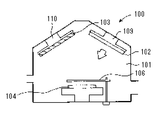
- a high frequency voltage is applied to the electrodes 109 and 110 in the sputtering chamber 101 to discharge Ar and generate plasma.
- the discharge is started, only the surface of the target 102 made of a material having a getter effect that easily adsorbs gas molecules is sputtered under the condition that ions in the plasma do not collide with the Al-based alloy target 103.
- impurities such as O 2 and N 2 remaining in the sputtering chamber 101 are gettered, and the concentration thereof is significantly reduced.
- the present invention has been made in view of the above circumstances, and it is possible to maintain the condition of the barrier layer film forming chamber without using a dummy wafer for chamber conditions, and to reduce the film forming process, the tunnel magnetoresistive effect
- An object is to provide a method for manufacturing an element. The present invention solves the above-described problems by the solving means described below.
- a tunnel magnetoresistive element is formed by sequentially laminating a first underlayer, a second underlayer, an antiferromagnetic layer, a fixed magnetic layer, a barrier layer, and a free magnetic layer on a wafer.
- a method for producing an effect element wherein the first underlayer is formed on the wafer using a target capable of obtaining a getter effect in a first chamber in which the barrier layer is formed, and then , Forming the second underlayer, the antiferromagnetic layer, and the pinned magnetic layer in the second chamber, and then forming the barrier layer in the first chamber, It is a requirement that the free magnetic layer be formed in the third chamber.
- a protective layer is formed as an upper layer of the free magnetic layer in the first chamber.
- the first underlayer is made of tantalum or titanium.
- the second underlayer is required to have a configuration in which a plurality of layers are stacked.
- the first underlayer is laminated by sputtering, and the getter effect generated at that time causes the first chamber to be simultaneously formed in the first chamber.
- Conditioning can be performed. This eliminates the need for a conditioning process using another dummy wafer.
- using tantalum or titanium as a material for forming the first underlayer is effective in that a large getter effect can be obtained.
- FIG. 5 is a schematic view showing an example of a film configuration of a tunnel magnetoresistive effect element formed by the procedure of FIG. 4.
- membrane structure of the tunnel magnetoresistive effect element formed into a film by the procedure of FIG. 1 is a schematic diagram showing an example of a TMR film forming apparatus commonly used in a method for manufacturing a tunnel magnetoresistive effect element according to an embodiment of the present invention and a method for manufacturing a tunnel magnetoresistive effect element according to a conventional embodiment. is there.
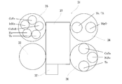
- FIG. 9 shows a configuration example of the TMR film forming apparatus 31 used in the manufacturing method.
- the TMR film forming apparatus 31 includes a cassette chamber 32 for setting a wafer, a wafer cleaning chamber 33 for performing a wafer cleaning process, a first chamber 34 for forming a barrier layer, and a fixed magnetic layer from a first underlayer.
- a second chamber 35 for forming a film and a third chamber 36 for forming a protective layer from the free magnetic layer are provided.
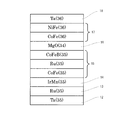
- FIG. 10 shows an example of a TMR film configuration formed by the TMR film forming apparatus 31.
- the numbers in parentheses indicate examples of chambers in which the layer is formed (34: first chamber, 35: second chamber, 36: third chamber).
- the first underlayer 12 is configured using Ta.
- the second underlayer 13 is configured using Ru.
- the antiferromagnetic layer 14 is configured using IrMn made of a Mn-based antiferromagnetic material.
- the pinned magnetic layer 15 is configured using a three-layer film of CoFe / Ru / CoFeB.
- the barrier layer 16 is configured using MgO which is an insulating material.
- the free magnetic layer 17 is configured using a CoFe / NiFe two-layer film.
- the protective layer 18 is configured using Ta.
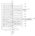
- FIG. 11 shows a flowchart for forming a TMR film. In FIG.
- the first wafer is a dummy wafer for conditioning the first chamber 34 for forming the barrier layer.
- the second wafer is a product wafer on which a TMR film is formed.
- the first dummy wafer set in the cassette chamber 32 in step S11 is transferred by a transfer mechanism (not shown) provided in the transfer chamber 37 and accommodated in the wafer cleaning chamber 33 (step S12). Thereafter, the dummy wafer is transferred to the first chamber 34, and the condition in the first chamber 34 is adjusted by depositing a material having a getter effect such as Ta or Ti (step S13). Then, the first dummy wafer returns to the cassette chamber 32 (step S14).
- the second product wafer is transferred to the wafer cleaning chamber 32 as described above (steps S21 and S22). Thereafter, the first underlayer 12, the second underlayer 13, the antiferromagnetic layer 14, and the fixed magnetic layer 15 are sequentially sputtered by being transferred to the second chamber 35 (step S23). Next, the product wafer is transferred to the first chamber 34, and the barrier layer 16 is formed by sputtering (step S24). Further, the product wafer is transferred to the third chamber 36, and the free magnetic layer 17 and the protective layer 18 are sequentially formed by sputtering (step S25). Thereafter, the product wafer returns to the cassette chamber 32, and the formation of the TMR film is completed (step S26).
- the film forming process of the first dummy wafer and the second product wafer in FIG. 11 is repeated.
- the above manufacturing method requires a dummy wafer sputtering process for adjusting the condition of the first chamber 34 for each product wafer before forming the TMR film.
- the manufacturing process of an element became long.
- the same number of condition dummy wafers as the product wafers for TMR film formation are required. Therefore, in the TMR film formation apparatus 31, the number of product wafers that can be set at one time is halved, that is, per batch. There was also a problem that the number of processed sheets was reduced.
- the tunnel magnetoresistive element manufacturing method disclosed below makes it possible to maintain the condition of the barrier layer film forming chamber (chamber) without using a chamber condition dummy wafer, thereby shortening the film forming process.
- a method for manufacturing a tunnel magnetoresistive effect element according to the first embodiment will be described.
- the TMR film forming apparatus used in the manufacturing method has the same basic configuration as the TMR film forming apparatus 31 used in the conventional tunnel magnetoresistive element manufacturing method (see FIG. 9).
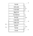
- the example of the film configuration of the tunnel magnetoresistive effect element by the manufacturing method according to the present embodiment shown in FIG. 2 is substantially the same as the example of the film configuration by the conventional manufacturing method shown in FIG.
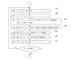
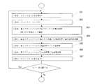
- FIG. 1 shows a flowchart of a manufacturing method (film formation process) according to the present embodiment.
- a product wafer for forming a TMR film is transferred from the cassette chamber 32 to the wafer cleaning chamber 33 (steps S31 and S32). Thereafter, the film is transferred into the first chamber 34 and film formation is performed using a Ti target.
- the Ti to be sputtered is laminated as the first underlayer 12 of the TMR film, and simultaneously has two functions for conditioning the first chamber 34 (step S33).
- the product wafer is transferred to the second chamber 35, and the second underlayer 13, the antiferromagnetic layer 14, and the pinned magnetic layer 15 are formed in this order (step S34).
- the film is transferred to the first chamber 34 to form the barrier layer 16 using MgO (step S35), and further transferred to the third chamber 36 to form the free magnetic layer 17 and the protective layer 18.
- Film is formed (step S36) and returned to the cassette chamber 32 (step S37).
- the configuration of the film forming apparatus for carrying out the manufacturing method according to the present embodiment uses, as an example, an apparatus having the same configuration as the apparatus according to the conventional manufacturing method, but is not limited thereto. It is not something. That is, if it is ensured that the film formation process of the first underlayer 12 is performed in a chamber used for film formation of the barrier layer 16, the other layers are formed by providing separate chambers. It is possible to employ various apparatus configurations.
- an example is shown in which Ti is used for conditioning the first chamber 34, and Ti formed in the first chamber 34 is the same as the first underlayer 12. It is the composition which becomes. (Table 1) Table 1 shows a comparison of characteristics with the tunnel magnetoresistive element according to the conventional manufacturing method.
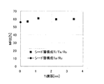
- FIG. 3 shows the Ti film thickness dependence of the tunnel magnetoresistive effect element having the configuration shown in FIG.
- the MR ratio characteristics are almost constant with respect to the Ti film thickness, and the MR ratio does not decrease.
- the tunnel magnetoresistive effect element manufactured by the manufacturing method according to the present embodiment can be manufactured without providing a dummy wafer and conditioning the chamber as in the conventional manufacturing method. It has been proved that it has characteristics comparable to conventional ones. That is, by using Ti having a getter effect for the base layer (first base layer 12) for forming the TMR film, the barrier layer 16 is formed without using a condition dummy wafer. The condition of the chamber 34 can be maintained.
- the first underlayer 12 may be made of Ta instead of Ti.
- the overall film configuration finally formed is the same as in the case of the third embodiment described later.
- the material is not limited to the above Ta and Ti, as long as it is a material that functions as the first underlayer and has a getter effect.
- FIG. 4 shows a flowchart of the manufacturing method according to the present embodiment (steps S41 to S47).
- the basic configuration is the same as the tunnel magnetoresistive effect element manufacturing method (film forming step) according to the first embodiment shown in FIG.
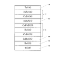
- FIG. 5 shows a film configuration of a tunnel magnetoresistive effect element formed in order from the bottom according to the flowchart of FIG. The material which comprises each layer was described, and the chamber in which film-forming was performed was displayed in the parenthesis.
- the film configuration of the tunnel magnetoresistive effect element according to the first embodiment shown in FIG. 2 is a configuration in which Ti (or Ta) is added as a lower layer to the conventional film configuration shown in FIG.
- the film configuration of the tunnel magnetoresistive effect element according to the present embodiment (second embodiment) shown in FIG. 5 is the second film formed in the second chamber 35 in the conventional film configuration shown in FIG.
- the lower layer (a layer using Ta) 13 a of the base layer is not provided, and Ti is formed as the first base layer 12 in the first chamber 34.
- Table 2 shows a comparison of characteristics with the tunnel magnetoresistive element according to the conventional manufacturing method. It has almost the same RA and MR ratio as before.
- FIG. 6 shows the Ti film thickness dependence of a tunnel magnetoresistive effect element having the configuration shown in FIG. The MR ratio characteristics are almost constant with respect to the Ti film thickness, and the MR ratio does not decrease. Similar to the first embodiment, in the second embodiment, as in the conventional manufacturing method, the manufacturing according to this embodiment can be performed without providing a separate dummy wafer and conditioning the chamber.
- FIG. 7 shows a flowchart of the manufacturing method according to the present embodiment (steps S51 to S57). The basic configuration of the flowchart is the same as that of the tunnel magnetoresistive effect element manufacturing method (film formation step) according to the second embodiment shown in FIG.
- the first underlayer 12 formed in the first chamber 34 is a film forming process using Ta.
- FIG. 8 shows a film configuration of a tunnel magnetoresistive effect element formed in order from the bottom according to the flowchart of FIG. The material which comprises each layer was described, and the chamber in which film-forming was performed was displayed in the parenthesis. It is different from the film configuration of the tunnel magnetoresistive effect element according to the second embodiment shown in FIG. 5 in that the first underlayer 12 is a Ta layer. (Table 3) (Table 4) Here, Table 3 shows a comparison of characteristics with the tunnel magnetoresistive effect element according to the conventional manufacturing method. It has almost the same RA and MR ratio as before.
- Table 4 shows a comparison of TMR characteristics in the wafer with the tunnel magnetoresistive effect element according to the conventional manufacturing method.
- the distribution in the RA wafer can be reduced by about 35% compared to the conventional case, and the MR ratio distribution can also be reduced by about 60%. The effect was seen.
- the same effects as in the first embodiment and the second embodiment are achieved.
- a product using Ti (or Ta) as a target in a chamber (first chamber) used for film formation of a barrier layer is used.
- the underlayer of the wafer (first underlayer) is formed and the Ti (or Ta) can also serve as the conditioning of the first chamber, it has been conventionally performed before the product wafer is formed.
- the sputtering process by the dummy wafer for the condition of the first chamber can be omitted, and the problem that the film forming process in the conventional manufacturing method becomes long is solved.
- there is no need to set a condition dummy wafer in the cassette chamber there is also an effect that the number of sheets that can be processed in one batch is increased, so that shortening of the manufacturing process (film forming process) is achieved synergistically. .
- the dummy wafer becomes unnecessary, the manufacturing cost can be reduced. It is also possible to improve the distribution in the wafer by adopting Ta as a material used for conditioning (which is also a material for the first underlayer).
Landscapes
- Engineering & Computer Science (AREA)
- Manufacturing & Machinery (AREA)
- Hall/Mr Elements (AREA)
- Magnetic Heads (AREA)
Abstract
Procédé de fabrication d'un élément à effet tunnel magnétorésistif permettant de maintenir l'état d'une chambre de dépôt de couche formant barrière sans utiliser une tranche à blanc pour le conditionnement de la chambre, et permettant de raccourcir le processus de formation d'un film. Le procédé de fabrication d'un élément à effet tunnel magnétorésistif est réalisé de telle sorte l'élément à effet tunnel magnétorésistif soit formé en stratifiant successivement une première sous-couche, une deuxième sous-couche, une couche antiferromagnétique, une couche magnétique fixe, une couche barrière et une couche magnétique libre sur une tranche. Dans une première chambre dans laquelle est effectué le dépôt de la couche barrière, on utilise une cible permettant d'obtenir des effets getter afin de déposer la première sous-couche sur la tranche. Puis, dans une deuxième chambre, la deuxième sous-couche, la couche antiferromagnétique et la couche magnétique fixe sont déposées. La couche barrière est ensuite déposée dans la première chambre, puis la couche magnétique libre est déposée dans la troisième chambre.
Priority Applications (1)
| Application Number | Priority Date | Filing Date | Title |
|---|---|---|---|
| PCT/JP2008/051617 WO2009096033A1 (fr) | 2008-02-01 | 2008-02-01 | Procédé de fabrication d'un élément à effet tunnel magnétorésistif |
Applications Claiming Priority (1)
| Application Number | Priority Date | Filing Date | Title |
|---|---|---|---|
| PCT/JP2008/051617 WO2009096033A1 (fr) | 2008-02-01 | 2008-02-01 | Procédé de fabrication d'un élément à effet tunnel magnétorésistif |
Publications (1)
| Publication Number | Publication Date |
|---|---|
| WO2009096033A1 true WO2009096033A1 (fr) | 2009-08-06 |
Family
ID=40912401
Family Applications (1)
| Application Number | Title | Priority Date | Filing Date |
|---|---|---|---|
| PCT/JP2008/051617 Ceased WO2009096033A1 (fr) | 2008-02-01 | 2008-02-01 | Procédé de fabrication d'un élément à effet tunnel magnétorésistif |
Country Status (1)
| Country | Link |
|---|---|
| WO (1) | WO2009096033A1 (fr) |
Citations (2)
| Publication number | Priority date | Publication date | Assignee | Title |
|---|---|---|---|---|
| JP2005333106A (ja) * | 2004-04-20 | 2005-12-02 | Ken Takahashi | 交換結合素子とその製造方法並びに交換結合素子を具備したデバイス |
| JP2007266584A (ja) * | 2006-03-03 | 2007-10-11 | Canon Anelva Corp | 磁気抵抗効果素子の製造方法及び製造装置 |
-
2008
- 2008-02-01 WO PCT/JP2008/051617 patent/WO2009096033A1/fr not_active Ceased
Patent Citations (2)
| Publication number | Priority date | Publication date | Assignee | Title |
|---|---|---|---|---|
| JP2005333106A (ja) * | 2004-04-20 | 2005-12-02 | Ken Takahashi | 交換結合素子とその製造方法並びに交換結合素子を具備したデバイス |
| JP2007266584A (ja) * | 2006-03-03 | 2007-10-11 | Canon Anelva Corp | 磁気抵抗効果素子の製造方法及び製造装置 |
Similar Documents
| Publication | Publication Date | Title |
|---|---|---|
| JP5341082B2 (ja) | トンネル磁気抵抗素子の製造方法および製造装置 | |
| US8728830B2 (en) | Manufacturing method of magneto-resistive element | |
| US8993351B2 (en) | Method of manufacturing tunneling magnetoresistive element | |
| CN103403215B (zh) | 制造设备 | |
| US10002973B2 (en) | Magnetic tunnel junction with an improved tunnel barrier | |
| US11552244B2 (en) | Magnetic tunnel junction structures and methods of manufacture thereof | |
| US20100080894A1 (en) | Fabricating method of magnetoresistive element, and storage medium | |
| US20100078310A1 (en) | Fabricating method of magnetoresistive element, and storage medium | |
| EP1973178A2 (fr) | Dispositif à effet de magnétorésistance et son procédé de production | |
| US7771570B2 (en) | Method and apparatus for depositing a magnetoresistive multilayer film | |
| WO2007105472A1 (fr) | Procede et appareil de fabrication d'element a magnetoresistance | |
| JP5689932B2 (ja) | トンネル磁気抵抗素子の製造方法 | |
| US20110084348A1 (en) | Magnetoresistance element, method of manufacturing the same, and storage medium used in the manufacturing method | |
| US10957849B2 (en) | Magnetic tunnel junctions with coupling-pinning layer lattice matching | |
| JPWO2010029701A1 (ja) | 磁気抵抗素子とその製造方法、該製造方法に用いる記憶媒体 | |
| JP2008277693A (ja) | トンネル磁気抵抗素子 |
Legal Events
| Date | Code | Title | Description |
|---|---|---|---|
| 121 | Ep: the epo has been informed by wipo that ep was designated in this application |
Ref document number: 08704326 Country of ref document: EP Kind code of ref document: A1 |
|
| NENP | Non-entry into the national phase |
Ref country code: DE |
|
| 122 | Ep: pct application non-entry in european phase |
Ref document number: 08704326 Country of ref document: EP Kind code of ref document: A1 |
|
| NENP | Non-entry into the national phase |
Ref country code: JP |