WO2009096352A1 - アリールスルホン酸化合物および電子受容性物質としての利用 - Google Patents
アリールスルホン酸化合物および電子受容性物質としての利用 Download PDFInfo
- Publication number
- WO2009096352A1 WO2009096352A1 PCT/JP2009/051169 JP2009051169W WO2009096352A1 WO 2009096352 A1 WO2009096352 A1 WO 2009096352A1 JP 2009051169 W JP2009051169 W JP 2009051169W WO 2009096352 A1 WO2009096352 A1 WO 2009096352A1
- Authority
- WO
- WIPO (PCT)
- Prior art keywords
- group
- acid compound
- charge transporting
- electron
- formula
- Prior art date
- Legal status (The legal status is an assumption and is not a legal conclusion. Google has not performed a legal analysis and makes no representation as to the accuracy of the status listed.)
- Ceased
Links
Images



Classifications
-
- H—ELECTRICITY
- H10—SEMICONDUCTOR DEVICES; ELECTRIC SOLID-STATE DEVICES NOT OTHERWISE PROVIDED FOR
- H10K—ORGANIC ELECTRIC SOLID-STATE DEVICES
- H10K85/00—Organic materials used in the body or electrodes of devices covered by this subclass
- H10K85/60—Organic compounds having low molecular weight
- H10K85/615—Polycyclic condensed aromatic hydrocarbons, e.g. anthracene
-
- C—CHEMISTRY; METALLURGY
- C07—ORGANIC CHEMISTRY
- C07C—ACYCLIC OR CARBOCYCLIC COMPOUNDS
- C07C309/00—Sulfonic acids; Halides, esters, or anhydrides thereof
- C07C309/01—Sulfonic acids
- C07C309/28—Sulfonic acids having sulfo groups bound to carbon atoms of six-membered aromatic rings of a carbon skeleton
- C07C309/41—Sulfonic acids having sulfo groups bound to carbon atoms of six-membered aromatic rings of a carbon skeleton containing singly-bound oxygen atoms bound to the carbon skeleton
- C07C309/43—Sulfonic acids having sulfo groups bound to carbon atoms of six-membered aromatic rings of a carbon skeleton containing singly-bound oxygen atoms bound to the carbon skeleton having at least one of the sulfo groups bound to a carbon atom of a six-membered aromatic ring being part of a condensed ring system
-
- C—CHEMISTRY; METALLURGY
- C09—DYES; PAINTS; POLISHES; NATURAL RESINS; ADHESIVES; COMPOSITIONS NOT OTHERWISE PROVIDED FOR; APPLICATIONS OF MATERIALS NOT OTHERWISE PROVIDED FOR
- C09K—MATERIALS FOR MISCELLANEOUS APPLICATIONS, NOT PROVIDED FOR ELSEWHERE
- C09K11/00—Luminescent materials, e.g. electroluminescent or chemiluminescent
- C09K11/06—Luminescent materials, e.g. electroluminescent or chemiluminescent containing organic luminescent materials
-
- H—ELECTRICITY
- H05—ELECTRIC TECHNIQUES NOT OTHERWISE PROVIDED FOR
- H05B—ELECTRIC HEATING; ELECTRIC LIGHT SOURCES NOT OTHERWISE PROVIDED FOR; CIRCUIT ARRANGEMENTS FOR ELECTRIC LIGHT SOURCES, IN GENERAL
- H05B33/00—Electroluminescent light sources
- H05B33/12—Light sources with substantially two-dimensional [2D] radiating surfaces
- H05B33/20—Light sources with substantially two-dimensional [2D] radiating surfaces characterised by the chemical or physical composition or the arrangement of the material in which the electroluminescent material is embedded
-
- H—ELECTRICITY
- H10—SEMICONDUCTOR DEVICES; ELECTRIC SOLID-STATE DEVICES NOT OTHERWISE PROVIDED FOR
- H10K—ORGANIC ELECTRIC SOLID-STATE DEVICES
- H10K50/00—Organic light-emitting devices
- H10K50/10—OLEDs or polymer light-emitting diodes [PLED]
- H10K50/14—Carrier transporting layers
-
- H—ELECTRICITY
- H10—SEMICONDUCTOR DEVICES; ELECTRIC SOLID-STATE DEVICES NOT OTHERWISE PROVIDED FOR
- H10K—ORGANIC ELECTRIC SOLID-STATE DEVICES
- H10K50/00—Organic light-emitting devices
- H10K50/10—OLEDs or polymer light-emitting diodes [PLED]
- H10K50/14—Carrier transporting layers
- H10K50/15—Hole transporting layers
-
- H—ELECTRICITY
- H10—SEMICONDUCTOR DEVICES; ELECTRIC SOLID-STATE DEVICES NOT OTHERWISE PROVIDED FOR
- H10K—ORGANIC ELECTRIC SOLID-STATE DEVICES
- H10K50/00—Organic light-emitting devices
- H10K50/10—OLEDs or polymer light-emitting diodes [PLED]
- H10K50/14—Carrier transporting layers
- H10K50/15—Hole transporting layers
- H10K50/155—Hole transporting layers comprising dopants
-
- C—CHEMISTRY; METALLURGY
- C09—DYES; PAINTS; POLISHES; NATURAL RESINS; ADHESIVES; COMPOSITIONS NOT OTHERWISE PROVIDED FOR; APPLICATIONS OF MATERIALS NOT OTHERWISE PROVIDED FOR
- C09K—MATERIALS FOR MISCELLANEOUS APPLICATIONS, NOT PROVIDED FOR ELSEWHERE
- C09K2211/00—Chemical nature of organic luminescent or tenebrescent compounds
- C09K2211/10—Non-macromolecular compounds
- C09K2211/1003—Carbocyclic compounds
- C09K2211/1011—Condensed systems
-
- H—ELECTRICITY
- H10—SEMICONDUCTOR DEVICES; ELECTRIC SOLID-STATE DEVICES NOT OTHERWISE PROVIDED FOR
- H10K—ORGANIC ELECTRIC SOLID-STATE DEVICES
- H10K2102/00—Constructional details relating to the organic devices covered by this subclass
Definitions
- the present invention relates to an aryl sulfonic acid compound and use of this compound as an electron accepting substance.
- a varnish containing an electron-accepting substance composed of an aryl sulfonic acid compound, a charge transporting thin film using the varnish, and an organic electroluminescence (hereinafter abbreviated as organic EL) using the charge transporting thin film There are elements.
- Organic EL elements especially low-molecular-weight organic EL (hereinafter abbreviated as OLED) elements
- OLED organic EL
- PLED organic EL
- Non-Patent Document 3 Applied Physics Letters, USA, 1996, 69, p. 2160-21612.
- Non-patent Document 4 Polyaniline-based materials
- Non-patent Document 5 Polyaniline-based materials
- Non-patent Document 5 Polyaniline-based materials
- Non-patent Document 6 Applied Physics Letters
- Is used as a hole transport layer (buffer layer) it has been reported that the same effect as an OLED element can be obtained.
- Non-patent Document 7 IEEE Transactions on Electron Devices, USA, 1997, Vol. 44, p. 1245-1248
- metal halides Non-patent Document 8: Applied Physics Letters, USA, 1997, 70, p. 152-154
- metal complexes Non-patent Document 9: Japanese) ⁇ Journal of Applied Physics (1999, Vol. 38, p.L1348-1350), etc.
- Patent Document 1 Japanese Patent Application Laid-Open No. 2002-151272.
- CuPC which is a general hole injection material in an OLED element, has severe irregularities, and has a drawback that characteristics are greatly deteriorated by mixing a small amount in another organic layer.
- polyaniline-based materials and polythiophene-based materials currently used for PLED elements include water that may promote element degradation as a solvent, limited solvent options, and material aggregation and low
- problems such as a limited coating method capable of forming a uniform film due to solubility.
- organic solvent-based charge transport varnish containing a low-molecular-weight oligoaniline-based material with high solubility the types of electron-accepting dopants that can be used are limited, and the heat-resistance of electron-accepting dopants
- problems such as low amorphousness may occur.
- a charge transporting varnish containing a low molecular weight charge transporting substance and a charge accepting dopant substance, particularly a varnish containing a crystalline substance it is generally difficult to form a film having high flatness.
- the present invention has been made in view of the above circumstances, and can achieve high uniform film-forming properties.
- An object of the present invention is to provide an aryl sulfonic acid compound suitable as an electron-accepting substance, which can realize excellent EL element characteristics.
- the present inventors can realize high uniform film forming properties, and in particular, by applying to OLED elements and PLED elements, it is possible to realize EL element characteristics excellent in low driving voltage, high luminous efficiency, long life, and the like.
- An arylsulfonic acid compound suitable as an electron accepting substance has been found and reported (Patent Document 2: International Publication No. 2006/025342 pamphlet). Although this aryl sulfonic acid compound is soluble in an organic solvent, there is room for improvement in its solubility.
- the present inventors have found an aryl sulfonic acid compound represented by the formula (1) having excellent solubility in an organic solvent, and combined this aryl sulfonic acid compound with a charge transporting host material.
- the compound can accept the electrons of the charge transporting host material and improve the charge transporting property. Therefore, when used as a hole injection layer of an OLED element or the like, it is possible to drive at a low voltage and improve luminous efficiency.
- the present invention has been completed.
- Ar is an arylsulfonic acid compound of 1 or 2 represented by the following formula (3), (Wherein R 1 to R 5 are independently of each other a hydrogen atom, a halogen atom, an alkyl group having 1 to 10 carbon atoms, a halogenated alkyl group having 1 to 10 carbon atoms, or a halogenated group having 2 to 10 carbon atoms. Represents an alkenyl group.) 4).
- Ar is an aryl sulfonic acid compound of 3 represented by the following formula (4), (Wherein R 3 represents a hydrogen atom, a halogen atom, an alkyl group having 1 to 10 carbon atoms, a halogenated alkyl group having 1 to 10 carbon atoms, or a halogenated alkenyl group having 2 to 10 carbon atoms.) 5).
- An electron-accepting substance comprising any one of the arylsulfonic acid compounds 1 to 4, 6).
- 5 a charge transporting varnish comprising an electron accepting material, a charge transporting material, and a solvent; 7).
- a charge transporting thin film comprising 5 electron accepting materials, and a charge transporting material, 8).
- An organic electroluminescence device having 7 charge transporting thin films is provided.
- the aryl sulfonic acid compound of the present invention not only exhibits amorphous solidity at room temperature, but also has high solubility in various organic solvents. Therefore, an organic solvent-based charge transporting varnish containing this compound as a dopant should be used. Thus, an amorphous solid thin film can be easily produced. Further, by using the thin film formed containing the aryl sulfonic acid compound of the present invention as a hole injection layer or a hole transport layer, the driving voltage of the organic EL element is lowered and the current efficiency of light emission is improved. In addition, a uniform light emitting surface can be obtained.
- the aryl sulfonic acid compound of the present invention can be used only with an organic solvent, unlike the aqueous solution-type charge transport varnish conventionally used, and prevents device deterioration due to moisture mixing into the EL device. You can also.
- the organic solvent-based charge transporting varnish containing the aryl sulfonic acid compound of the present invention as a charge-accepting dopant substance can be applied to capacitor electrode protective films, antistatic films, ion conductive films, solar cell applications, fuel cells, etc. It is.
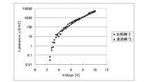
- FIG. 6 is a diagram showing voltage-luminance characteristics of OLED elements fabricated in Examples 9 to 11 and Comparative Example 3.
- FIG. 6 is a diagram showing voltage-current density characteristics of OLED elements fabricated in Examples 9 to 11 and Comparative Example 3.
- FIG. 6 is a graph showing voltage-luminance characteristics of OLED elements fabricated in Examples 12 to 14 and Comparative Example 3.
- FIG. 6 is a graph showing voltage-current density characteristics of OLED elements fabricated in Examples 12 to 14 and Comparative Example 3. It is a figure which shows the voltage-luminance characteristic of the OLED element produced in Example 15 and Comparative Example 3. It is a figure which shows the voltage-current density characteristic of the OLED element produced in Example 15 and Comparative Example 3.
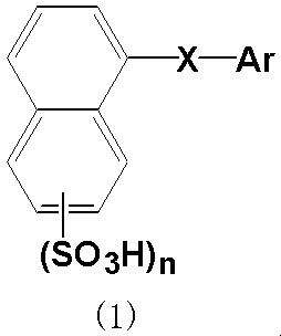
- the arylsulfonic acid compound according to the present invention is represented by the formula (1).
- X represents O, S or NH, and O is particularly preferable because of easy synthesis.
- Ar means an aryl group.
- the aryl group include aryl groups such as a phenyl group, a xylyl group, a tolyl group, a biphenyl group, and a naphthyl group, and these aryl groups may have a substituent.
- substituents examples include a hydroxyl group, an amino group, a silanol group, a thiol group, a carboxyl group, a phosphate group, a phosphate ester group, an ester group, a thioester group, an amide group, a nitro group, a cyano group, a monovalent hydrocarbon group, An organooxy group, an organoamino group, an organosilyl group, an organothio group, an acyl group, a sulfone group, a halogen atom, and the like are exemplified, but not limited thereto.
- monovalent hydrocarbon groups include methyl, ethyl, n-propyl, i-propyl, n-butyl, i-butyl, t-butyl, n-hexyl, and n-octyl.
- alkyl group such as 2-ethylhexyl group and decyl group
- cycloalkyl group such as cyclopentyl group and cyclohexyl group
- bicycloalkyl group such as bicyclohexyl group
- vinyl group 1-propenyl group, 2-propenyl group and isopropenyl group , 1-methyl-2-propenyl group, alkenyl group such as 1 or 2 or 3-butenyl group, hexenyl group
- aryl group such as phenyl group, xylyl group, tolyl group, biphenyl group, naphthyl group
- benzyl group, phenylethyl Group, aralkyl group such as phenylcyclohexyl group, etc., or some or all of the hydrogen atoms of these monovalent hydrocarbon groups are halogenated.
- Atom, a hydroxyl group, an alkoxy group include those substituted with a
- organooxy group examples include an alkoxy group, an alkenyloxy group, and an aryloxy group.
- alkyl group, alkenyl group, and aryl group examples include the same substituents as exemplified above. It is done.
- Specific examples of the organoamino group include methylamino group, ethylamino group, propylamino group, butylamino group, pentylamino group, hexylamino group, heptylamino group, octylamino group, nonylamino group, decylamino group, and laurylamino group.
- Alkylamino groups such as dimethylamino groups, diethylamino groups, dipropylamino groups, dibutylamino groups, dipentylamino groups, dihexylamino groups, diheptylamino groups, dioctylamino groups, dinonylamino groups, and didecylamino groups;
- a dicycloalkylamino group such as a cyclohexylamino group; a morpholino group, and the like.
- organosilyl group examples include trimethylsilyl group, triethylsilyl group, tripropylsilyl group, tributylsilyl group, tripentylsilyl group, trihexylsilyl group, pentyldimethylsilyl group, hexyldimethylsilyl group, octyldimethylsilyl group, Examples include decyldimethylsilyl group.
- organothio group examples include alkylthio groups such as methylthio group, ethylthio group, propylthio group, butylthio group, pentylthio group, hexylthio group, heptylthio group, octylthio group, nonylthio group, decylthio group, and laurylthio group.
- acyl group examples include formyl group, acetyl group, propionyl group, butyryl group, isobutyryl group, valeryl group, isovaleryl group, benzoyl group and the like.
- halogen atom examples include fluorine, chlorine, bromine, and iodine atoms.
- the monovalent hydrocarbon group, organooxy group, organoamino group, organoamino group, organosilyl group, organothio group, and acyl group particularly have Although not limited, it generally has 1 to 20 carbon atoms, preferably 1 to 8 carbon atoms.
- a fluorine atom, a sulfone group, a cyano group, an organooxy group, an alkyl group, and an organosilyl group are more preferable.
- the substituents may be connected to each other and may include a cyclic part.
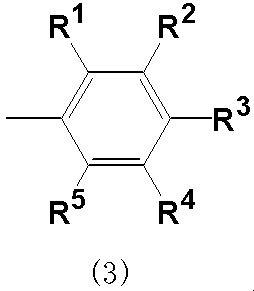
- an aryl group represented by the following formula (3) is preferably used.
- R 1 to R 5 are each independently a hydrogen atom, a halogen atom, an alkyl group having 1 to 10 carbon atoms, a halogenated alkyl group having 1 to 10 carbon atoms, or an alkenyl halide having 2 to 10 carbon atoms. Indicates a group.
- the halogen atom may be any of chlorine, bromine, fluorine, and iodine atoms. In the present invention, a fluorine atom is particularly preferable.
- alkyl group having 1 to 10 carbon atoms examples include methyl group, ethyl group, n-propyl group, i-propyl group, n-butyl group, i-butyl group, t-butyl group, n-pentyl group, and n-hexyl.
- Examples of the halogenated alkyl group having 1 to 10 carbon atoms include trifluoromethyl group, 2,2,2-trifluoroethyl group, 1,1,2,2,2-pentafluoroethyl group, 3,3,3- Trifluoropropyl group, 2,2,3,3,3-pentafluoropropyl group, 1,1,2,2,3,3,3-heptafluoropropyl group, 4,4,4-trifluorobutyl group, 3,3,4,4,4-pentafluorobutyl group, 2,2,3,3,4,4,4-heptafluorobutyl group, 1,1,2,2,3,3,4,4, Examples include 4-nonafluorobutyl group.
- Examples of the alkenyl halide having 2 to 10 carbon atoms include a perfluorovinyl group, a perfluoropropenyl group (allyl group), and a perfluorobutenyl group.
- an aryl group represented by the following formula (4) in consideration of further increasing the solubility in an organic solvent.
- R 3 represents a hydrogen atom, a halogen atom, an alkyl group having 1 to 10 carbon atoms, a halogenated alkyl group having 1 to 10 carbon atoms, or a halogenated alkenyl group having 2 to 10 carbon atoms.
- a halogenated alkyl group and a halogenated alkynyl group are preferable, and a trifluoromethyl group and a perfluoropropenyl group are more preferable.
- arylsulfonic acid compound represented by Formula (1) It does not specifically limit as a manufacturing method of the arylsulfonic acid compound represented by Formula (1), It can select suitably from conventionally well-known various methods. For example, it can be obtained by reacting the above-mentioned reagent for giving an aryl group to the XH group of the naphthalenesulfonic acid compound represented by the following formula (5).
- the reaction method is not particularly limited, and for example, a general nucleophilic substitution reaction can be used.
- reagents examples include perfluorobenzene, perfluorotoluene, 3- (pentafluorophenyl) pentafluoro-1-propene, perfluorobiphenyl, octafluoronaphthalene, perfluorobutylbenzene, perfluorophenanthrene, Aromatic (aryl) compounds substituted with halogen atoms such as perfluoroacenaphthylene and perfluorofluorene can be mentioned.
- a catalyst can be used.
- the catalyst include lithium, potassium, lithium hydride, sodium hydride, t-butoxy lithium, t-butoxy sodium, t-butoxy potassium, lithium-diisopropylamide, n-butyl lithium, s-butyl lithium, t- Butyllithium, lithium hexamethyldisilazide, sodium hexamethyldisilazide, potassium hexamethyldisilazide, lithium hydroxide, sodium hydroxide, potassium hydroxide, barium hydroxide, barium oxide, lithium carbonate, sodium carbonate, carbonic acid Bases such as potassium, cesium carbonate, calcium carbonate, sodium hydrogen carbonate, triethylamine, diisopropylethylamine, tetramethylethylenediamine, triethylenediamine, pyridine, dimethylaminopyridine, imidazole; hydrochlor
- the reaction solvent is preferably an aprotic polar organic solvent.
- N, N-dimethylformamide, N, N-dimethylacetamide, N-methylpyrrolidone, 1,3-dimethyl-2-imidazolidinone, dimethyl sulfoxide, tetrahydrofuran , Dioxane and the like are preferred.
- the aryl sulfonic acid compound (5) has a relatively low solubility in an organic solvent, a solvent having a high solubility and a low thermal decomposability is preferable. Therefore, among the above solvents, 1,3-dimethyl-2- Imidazolidinone and N-methylpyrrolidone are preferred.
- the reaction temperature is usually from ⁇ 50 ° C.
- reaction time is usually 0.1 to 100 hours. After completion of the reaction, it can be purified by evaporating the reaction solvent, protonating the sulfonate with a cation exchange resin, extraction with a solvent such as methanol, reprecipitation.
- the arylsulfonic acid compound can be obtained by a general sulfonation reaction using concentrated sulfuric acid, fuming sulfuric acid, and halosulfuric acid for the aryl compound.
- the above-described arylsulfonic acid compound of the present invention has an electron accepting property and can be suitably used as an electron accepting substance.
- the charge transporting varnish contains at least two kinds of substances, a charge transporting substance which is a main body of the charge transport mechanism, and an electron accepting substance represented by the above formula (1) in a solvent.
- the electron-accepting substance is used for improving the charge transporting ability and film formation uniformity, and is synonymous with the charge-accepting dopant substance.
- these substances may be completely dissolved in a solvent or may be uniformly dispersed.
- the charge transport property is synonymous with conductivity, and in the present invention, is synonymous with hole transport property.
- the charge transport varnish itself may have a charge transport property, or the solid film obtained from the varnish may have a charge transport property.
- the charge transporting substance used in the present invention is not particularly limited as long as it is a charge transporting oligomer or polymer that can be dissolved or uniformly dispersed by a solvent, but it may be an oligomer having one type of continuous conjugated units or different continuous ones. Oligomers having a combination of conjugated units are desirable.
- the conjugated unit is not particularly limited as long as it is an atom capable of transporting a charge, an aromatic ring, or a conjugated group, but is preferably a substituted or unsubstituted divalent to tetravalent aniline group, thiophene group, furan group, pyrrole.
- Group ethynylene group, vinylene group, phenylene group, naphthalene group, oxadiazole group, quinoline group, silole group, silicon atom, pyridine group, phenylene vinylene group, fluorene group, carbazole group, triarylamine group, metal- or none
- Examples include a metal-phthalocyanine group, a metal- or metal-free porphyrin group, and the like.
- substituents are each independently a hydrogen atom, a halogen atom, a hydroxyl group, an amino group, a silanol group, a thiol group, a carboxyl group, a sulfone group, a phosphate group, a phosphate ester group, an ester group, a thioester group, Examples include an amide group, a nitro group, a monovalent hydrocarbon group, an organooxy group, an organoamino group, an organosilyl group, an organothio group, and an acyl group. These functional groups are further substituted with any of the functional groups. May be.
- halogen atom monovalent hydrocarbon group, organooxy group, organoamino group, organosilyl group, organothio group, and acyl group
- Preferred substituents include fluorine atoms, sulfone groups, substituted or unsubstituted organooxy groups, alkyl groups, and organosilyl groups.
- the conjugated chain formed by coupling conjugated units may include a cyclic part.
- the number average molecular weight of the charge transporting substance is preferably 5000 or less in view of enhancing solubility, and is preferably 200 or more in order to exhibit low volatility and charge transportability.
- a substance having high solubility in at least one kind of solvent is good, and a substance having high solubility in at least one kind of solvent may have a number average molecular weight of 5,000 to 500,000.
- an oligoaniline derivative described in JP-A No. 2002-151272 is preferably used. That is, an oligoaniline derivative represented by the formula (6) is preferable.
- Examples of the monovalent hydrocarbon group, organooxy group and acyl group in the following R 6 to R 16 include the same substituents as described above.
- R 6 represents a hydrogen atom, a monovalent hydrocarbon group, or an organooxy group
- R 7 and R 8 each independently represent a hydrogen atom or a monovalent hydrocarbon group
- D 1 and D 2 each independently represents the following formula (7) or (8)
- R 9 to R 16 each independently represents a hydrogen atom, a hydroxyl group, a monovalent hydrocarbon group, an organooxy group, an acyl group, or a sulfone group, and s and t are Each independently represents an integer of 1 or more and satisfies s + t ⁇ 20. )
- the charge transporting property of the resulting charge transporting thin film is improved when the ⁇ -conjugated system in the molecule is expanded as much as possible, in particular, with the oligoaniline derivative represented by the formula (9) or its oxidant. It is preferable to use a certain quinonediimine derivative.
- the substituents having the same symbols may be the same or different at the same time.
- s + t is preferably 4 or more from the viewpoint of exhibiting good charge transportability, and is 16 or less from the viewpoint of ensuring solubility in a solvent. preferable.
- R 6 is a hydrogen atom and R 8 is a phenyl group, that is, it is preferable that both ends of the oligoaniline derivative of the formula (9) are sealed with a phenyl group. Only one kind of these charge transport materials may be used, or two or more kinds of materials may be used in combination.
- oligoanilines soluble in organic solvents such as phenyltetraaniline, phenylpentaaniline, tetraaniline (aniline tetramer), and octaaniline (aniline octamer). Derivatives.
- the method for synthesizing the charge transporting substance is not particularly limited.
- the literature Bulletin of Chemical Society of Japan, 1994, Vol. 67, p. 1749-1752, Synthetic Metals, USA, 1997, 84, p. 119-120, for example, the literature, Heterocycles, 1987, Vol. 26, p. 939-942, Heterocycles, 1987, 26, p. And oligothiophene synthesis methods described in 1793-1796.
- the blending ratio of the charge transporting substance and the aryl sulfonic acid compound in the charge transporting varnish of the present invention is not particularly limited, but considering that the luminance characteristics and current density characteristics of the obtained organic EL device are further improved.
- the amount is preferably in an amount of 0.5-2.
- a highly soluble solvent capable of dissolving the charge transporting substance and the charge accepting substance satisfactorily is used at a ratio of 5 to 100% by mass with respect to the total solvent used in the varnish. May be.
- the charge transporting substance and the charge accepting substance are completely dissolved or uniformly dispersed in the varnish by the highly soluble solvent.
- the highly soluble solvent is not particularly limited, and examples thereof include water, methanol, N, N-dimethylformamide, N, N-dimethylacetamide, N-methylpyrrolidone, 1,3-dimethyl-2-imidazolide. Non, dimethyl sulfoxide, chloroform, toluene, methanol and the like can be mentioned.
- the charge transporting varnish of the present invention preferably contains at least one high-viscosity organic solvent having a viscosity of 10 to 200 mPa ⁇ s at 20 ° C. and a boiling point of 50 to 300 ° C. at normal pressure. Further, the charge transporting varnish preferably contains an organic solvent having a viscosity of 50 to 150 mPa ⁇ s at 20 ° C. and a boiling point of 150 to 250 ° C. at normal pressure.
- the high-viscosity organic solvent is not particularly limited.
- cyclohexanol ethylene glycol, ethylene glycol diglycidyl ether, 1,3-octylene glycol, diethylene glycol, dipropylene glycol, triethylene glycol, tripropylene glycol 1,3-butanediol, 1,4-butanediol, propylene glycol, hexylene glycol and the like.
- the addition ratio of the high-viscosity organic solvent to the whole solvent used in the varnish of the present invention is preferably in the range where no solid precipitates, and the addition ratio should be 5 to 80% by mass as long as no solid precipitates. Can do.
- solvents that can impart film flatness during firing are used as a whole solvent for the varnish.
- 1 to 90% by mass preferably 1 to 50% by mass, can be mixed.
- a solvent is not particularly limited, and examples thereof include butyl cellosolve, diethylene glycol diethyl ether, dipropylene glycol monomethyl ether, ethyl carbitol, diacetone alcohol, ⁇ -butyrolactone, and ethyl lactate.
- a charge transporting thin film can be formed on a substrate by applying the charge transporting varnish described above on the substrate and evaporating the solvent.
- the method for applying the varnish is not particularly limited, and examples thereof include a dipping method, a spin coating method, a spray method, an ink jet method, a transfer printing method, a roll coating method, and a brush coating method.
- a membrane is possible.
- the method for evaporating the solvent is not particularly limited, however, using a hot plate or an oven, evaporation is performed in an appropriate atmosphere, that is, in an atmosphere such as air, an inert gas such as nitrogen, in a vacuum, etc., to form a uniform film. It is possible to obtain a film having a surface.
- the baking temperature is not particularly limited as long as the solvent can be evaporated, but 40 to 250 ° C. is preferable. In order to develop a higher uniform film forming property and to allow the reaction to proceed on the substrate, two or more stages of temperature changes may be applied.
- the film thickness of the charge transporting thin film obtained by coating and evaporation operations is not particularly limited, but is preferably 5 to 200 nm when used as a charge injection layer in an organic EL device.
- a method for changing the film thickness there are methods such as a change in the solid content concentration in the varnish and a change in the amount of the solution on the substrate during coating.
- Examples of the method for producing an OLED element using the charge transporting varnish of the present invention and the materials used include, but are not limited to, the following methods and materials. It is preferable that the electrode substrate to be used is cleaned in advance by washing with a detergent, alcohol, pure water or the like, and the anode substrate is subjected to surface treatment such as ozone treatment or oxygen-plasma treatment immediately before use. However, when the anode material is mainly composed of an organic material, the surface treatment may not be performed.
- a hole transporting varnish for an OLED element When using a hole transporting varnish for an OLED element, for example, the following method may be employed. That is, a hole transporting thin film is formed on the electrode by the above film manufacturing method using the hole transporting varnish for the anode substrate. This is introduced into a vacuum deposition apparatus, and a hole transport layer, a light emitting layer, an electron transport layer, an electron injection layer, and a cathode metal are sequentially deposited to form an OLED element. At this time, a carrier block layer may be provided between arbitrary layers in order to control the light emitting region.
- anode material examples include transparent electrodes typified by indium tin oxide (ITO) and indium zinc oxide (IZO), and those subjected to planarization treatment are preferable.
- ITO indium tin oxide
- IZO indium zinc oxide
- Polythiophene derivatives having high charge transportability and polyanilines can also be used.
- TPD triphenylamine dimer derivative
- ⁇ -NPD ⁇ -naphthyldiphenylamine dimer
- Spiro-TAD spiro-dimer
- Triarylamines such as 4,4 ′, 4 ′′ -tris [3-methylphenyl (phenyl) amino] triphenylamine (m-MTDATA), 4,4 ′, 4 ′′ -tris [1-naphthyl (phenyl) ) Amino] triphenylamine (1-TNATA) and other starburst amines, 5,5 ′′ -bis- ⁇ 4- [bis (4-methylphenyl) amino] phenyl ⁇ -2,2 ′: 5 ′,
- Materials for forming the light emitting layer include tris (8-quinolinolato) aluminum (III) (Alq 3 ), bis (8-quinolinolato) zinc (II) (Znq 2 ), bis (2-methyl-8-quinolinolato) ( Examples thereof include p-phenylphenolate) aluminum (III) (BAlq), 4,4′-bis (2,2-diphenylvinyl) biphenyl (DPVBi), and the like.
- the light-emitting layer may be formed by co-evaporation of an electron transport material or a hole transport material and a light-emitting dopant.
- Examples of the electron transport material include Alq 3 , BAlq, DPVBi, (2- (4-biphenyl) -5- (4-t-butylphenyl) -1,3,4-oxadiazole) (PBD), triazole derivatives ( TAZ), bathocuproine (BCP), silole derivatives and the like.
- Examples of the luminescent dopant include quinacridone, rubrene, coumarin 540, 4- (dicyanomethylene) -2-methyl-6- (p-dimethylaminostyryl) -4H-pyran (DCM), tris (2-phenylpyridine) iridium ( III) (Ir (ppy) 3 ), (1,10-phenanthroline) -tris (4,4,4-trifluoro-1- (2-thienyl) -butane-1,3-dionate) europium (III) ( Eu (TTA) 3 phen) and the like.
- Examples of the material for forming the carrier block layer include PBD, TAZ, and BCP.
- lithium oxide Li 2 O
- magnesium oxide MgO
- alumina Al 2 O 3
- lithium fluoride LiF
- magnesium fluoride MgF 2
- strontium fluoride SrF 2
- Lithium quinonolide Liq
- lithium acetylacetonate complex Li (acac)
- lithium acetate lithium benzoate and the like.
- the cathode material include aluminum, magnesium-silver alloy, aluminum-lithium alloy, lithium, sodium, potassium, cesium and the like.
- the charge transporting varnish of the present invention is used for an OLED element
- the following method may be employed.
- An electron transporting thin film is produced on the cathode substrate using the electron transporting varnish, introduced into a vacuum deposition apparatus, and using the same materials as described above, an electron transporting layer, a light emitting layer, a hole transporting layer, After the hole injection layer is formed, an anode material is formed by a method such as sputtering to form an OLED element.
- Examples of the method for producing a PLED element using the charge transporting varnish of the present invention include the following methods, but are not limited thereto.
- the charge transport property of the present invention is formed by forming a light emitting charge transporting polymer layer instead of performing vacuum deposition operation of the hole transport layer, the light emitting layer, the electron transport layer, and the electron injection layer.
- a PLED element including a charge transporting thin film formed of varnish can be produced.
- the hole transporting varnish is applied to the anode substrate by the above method to produce a hole transporting thin film on the electrode, and a light emitting charge transporting polymer layer is formed thereon. Further, a cathode electrode is deposited to form a PLED element.
- the electron transporting varnish is used for the cathode substrate, an electron transporting thin film is formed on the electrode by the above method, a light emitting charge transporting polymer layer is formed thereon, and the anode electrode is sputtered. , Vapor deposition, spin coating, etc. to produce a PLED element.
- the same materials as those exemplified for the OLED element can be used, and the same cleaning treatment and surface treatment can be performed.
- a method for forming a light emitting charge transporting polymer layer a solvent is added to a light emitting charge transporting polymer material or a material to which a light emitting dopant is added and dissolved or uniformly dispersed to transport holes. And a method of forming a film by evaporation of a solvent after coating on an electrode substrate on which a conductive thin film is formed.
- Examples of the light-emitting charge transporting polymer material include polyfluorene derivatives such as poly (9,9-dialkylfluorene) (PDAF), poly (2-methoxy-5- (2′-ethylhexoxy) -1,4-phenylene vinylene, and the like. And polyphenylene vinylene derivatives such as (MEH-PPV), polythiophene derivatives such as poly (3-alkylthiophene) (PAT), and polyvinylcarbazole (PVCz).
- polyfluorene derivatives such as poly (9,9-dialkylfluorene) (PDAF), poly (2-methoxy-5- (2′-ethylhexoxy) -1,4-phenylene vinylene, and the like.
- polyphenylene vinylene derivatives such as (MEH-PPV)
- polythiophene derivatives such as poly (3-alkylthiophene) (PAT)
- PVCz polyvinylcarbazol
- Examples of the solvent include toluene, xylene, chloroform and the like.
- Examples of the dissolution or uniform dispersion method include a method of dissolving or uniformly dispersing by a method such as stirring, heating and stirring, and ultrasonic dispersion.
- the application method is not particularly limited, and examples thereof include a dipping method, a spin coating method, a transfer printing method, a roll coating method, and brush coating.
- the application is preferably performed under an inert gas such as nitrogen or argon.
- Examples of the solvent evaporation method include a method of heating in an oven or a hot plate under an inert gas or in a vacuum.
- PTA phenyltetraaniline
- reaction solution was filtered, and the residue was washed successively with toluene and ether and dried to obtain silver crystals.
- 25 parts by mass of dioxane and 0.2 equivalent of hydrazine monohydrate were added to the obtained crystal, and the reaction system was purged with nitrogen, and then heated to reflux to dissolve the crystal.
- 25 parts by mass of toluene was added to the crystal to suspend the solution, and after heating to reflux, 10 parts by mass of dioxane was further added to dissolve by heating to reflux, and the resulting solution was filtered while hot. .
- Example 1 A perfluorotoluene naphthalene sulfonic acid compound (hereinafter abbreviated as 7FNS-1) was synthesized according to the following reaction formula.
- Example 2 A perfluoroallylbenzene naphthalenesulfonic acid compound (hereinafter abbreviated as 9FNS-1) was synthesized according to the following reaction formula.
- Example 3 A dicyanoperfluorotoluenesulfonic acid compound (hereinafter abbreviated as 3FNS-1) was synthesized according to the following reaction formula.
- Example 4 A cyanoperfluorotoluenesulfonic acid compound (hereinafter abbreviated as 4FNS-2) was synthesized according to the following reaction formula.
- NSO-2 naphthalenedisulfonic acid compound
- NSO-2 was synthesized according to International Publication No. 2006/025342. 934 mg of well-dried sodium 1-naphthol-3,6-disulfonate (manufactured by Tokyo Chemical Industry Co., Ltd.), 450 mg of perfluorobiphenyl, 166 mg of 60% sodium hydride, and anhydrous N, N— under a nitrogen atmosphere 50 ml of dimethylimidazolidinone was sequentially added and the reaction system was purged with nitrogen, followed by stirring at 80 ° C. for 43 hours. After allowing to cool to room temperature, water was added to stop the reaction, and the mixture was concentrated to dryness under reduced pressure.
- a uniform thin film having a thickness of about 30 nm is formed on an ITO glass substrate by spin coating, and then introduced into a vacuum deposition apparatus, and ⁇ -NPD, Alq 3 , LiF, and Al are sequentially deposited to obtain an OLED element.
- the film thicknesses were 30 nm, 50 nm, 1 nm, and 120 nm, respectively, and the vapor deposition operation was performed after the pressure was 8 ⁇ 10 ⁇ 4 Pa or less.
- the vapor deposition rate was 0.3 to 0.4 nm / s excluding LiF. LiF was set to 0.02 to 0.04 nm / s.
- the transfer operation between the vapor deposition operations was performed in a vacuum.
- a varnish was prepared by dissolving in a solvent of 2 to a solid content of 2.8% by mass. After using this varnish to produce a thin film in the same manner as in Comparative Example 3, a vapor deposition operation was performed in the same manner as in Comparative Example 3 to obtain an OLED element.
- Example 10 An OLED element was obtained in the same manner as in Example 9, except that 1.0 molar equivalent of 7FNS-1 obtained in Example 1 was used.
- Example 11 An OLED element was obtained in the same manner as in Example 9, except that 3.0 molar equivalents of 7FNS-1 obtained in Example 1 was used.
- a varnish was prepared by dissolving in a solvent of 2 to a solid content of 2.8% by mass. After using this varnish to produce a thin film in the same manner as in Comparative Example 3, a vapor deposition operation was performed in the same manner as in Comparative Example 3 to obtain an OLED element.
- Example 13 An OLED element was obtained in the same manner as in Example 12 except that 1.0 molar equivalent of 9FNS-1 obtained in Example 2 was used.
- Example 14 An OLED element was obtained in the same manner as in Example 12 except that 3.0 molar equivalent of 9FNS-1 obtained in Example 2 was used.
- Example 15 An OLED element was obtained in the same manner as in Example 12, except that 2.0 molar equivalents of 4FNS-2 obtained in Example 4 was used.
- the characteristics of the OLED elements fabricated in Examples 9 to 15 and Comparative Example 3 were evaluated. A comparison of Examples 9 to 11 and Comparative Example 3 is shown in FIGS. 1 and 2, a comparison of Examples 12 to 14 and Comparative Example 3 is shown in FIGS. 3 and 4, and a comparison of Example 15 and Comparative Example 3 is shown in FIG. And shown in FIG. In addition, the characteristic of the OLED element was measured using the organic electroluminescent luminous efficiency measuring apparatus (EL1003, product made from a precise gauge).
- EL1003 organic electroluminescent luminous efficiency measuring apparatus
- the OLED devices fabricated in Examples 9 and 10 are particularly superior in voltage-luminance and voltage-current density as compared with the device of Comparative Example 3.
- Example 11 it turns out that a brightness
- FIGS. 3 and 4 it can be seen that the OLED device fabricated in Example 12 is particularly superior in voltage-luminance and voltage-current density as compared with the device of Comparative Example 3.
- the luminance and current density are superior to those of Comparative Example 3 in the region where the voltage is 10 V or less.
- FIGS. 5 and 6 it can be seen that the OLED device fabricated in Example 15 has the same or better properties than the device of Comparative Example 3.
Landscapes
- Chemical & Material Sciences (AREA)
- Organic Chemistry (AREA)
- Engineering & Computer Science (AREA)
- Materials Engineering (AREA)
- Physics & Mathematics (AREA)
- Optics & Photonics (AREA)
- Spectroscopy & Molecular Physics (AREA)
- Electroluminescent Light Sources (AREA)
- Organic Low-Molecular-Weight Compounds And Preparation Thereof (AREA)
Abstract
Description
また、ケンブリッジ大によって高分子発光材料を用いた有機EL(以下、PLEDと略す)素子が見出され(非特許文献2:ネイチャー(Nature)、英国、1990年、第347巻、p.539-541)、近年の高分子有機EL素子の特性は、従来のOLED素子に引けを取らないレベルにまで向上している。
一方、PLED素子では、ポリアニリン系材料(非特許文献4:ネイチャー(Nature)、英国、1992年、第357巻、p.477-479、非特許文献5:アプライド・フィジックス・レターズ(Applied Physics Letters)、米国、1994年、64巻、p.1245-1247)や、ポリチオフェン系材料(非特許文献6:アプライド・フィジックス・レターズ(Applied Physics Letters)、米国、1998年、72巻、p.2660-2662)を、正孔輸送層(バッファ層)として用いることで、OLED素子と同様の効果が得られることが報告されている。
しかし、OLED素子における一般的な正孔注入材料であるCuPCは凹凸が激しく、他の有機層に微量混入することによって大きく特性を低下させるなどの欠点がある。
また、現在、PLED素子に用いられているポリアニリン系材料、ポリチオフェン系材料は、素子劣化を促進する可能性のある水を溶剤として含むこと、溶剤の選択肢が限られること、および材料の凝集や低溶解性によって均一な成膜ができる塗布法が限られることなどの問題点を含んでいる。
さらに、溶解性の高い低分子オリゴアニリン系材料を含む有機溶剤系の電荷輸送性ワニスを用いた場合にも、使用可能な電子受容性ドーパントの種類が限られたり、電子受容性ドーパントの耐熱性および非晶性が低い等の問題が生じたりする場合がある。また、低分子量の電荷輸送性物質および電荷受容性ドーパント物質を含む電荷輸送性ワニス、特に結晶性物質を含むワニスにおいては、一般に高い平坦性を示す成膜が難しい場合がある。
このアリールスルホン酸化合物は、有機溶剤に可溶ではあるものの、その溶解性については改良の余地があった。
そこで、本発明者らは鋭意検討を重ねた結果、有機溶剤に対する溶解性に優れた式(1)で示されるアリールスルホン酸化合物を見出すとともに、このアリールスルホン酸化合物を電荷輸送性ホスト物質と組み合わせると、当該化合物が電荷輸送性ホスト物質の有する電子を受容して電荷輸送性を向上し得るため、OLED素子等の正孔注入層として用いた場合に、低電圧駆動、発光効率の向上を可能にすることを見出し、本発明を完成した。
1. 式(1)で表されることを特徴とするアリールスルホン酸化合物、
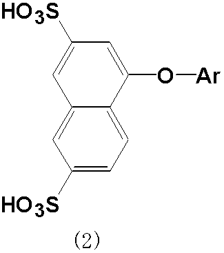
2. 式(2)で表される1のアリールスルホン酸化合物、
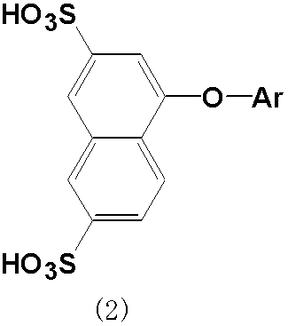
3. 前記Arが、下記式(3)で示される1または2のアリールスルホン酸化合物、
4. 前記Arが、下記式(4)で示される3のアリールスルホン酸化合物、
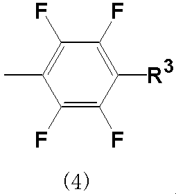
5. 1~4のいずれかのアリールスルホン酸化合物からなる電子受容性物質、
6. 5の電子受容性物質、電荷輸送性物質、および溶剤を含む電荷輸送性ワニス、
7. 5の電子受容性物質、および電荷輸送性物質を含む電荷輸送性薄膜、
8. 7の電荷輸送性薄膜を有する有機エレクトロルミネッセンス素子
を提供する。
また、本発明のアリールスルホン酸化合物を含んで形成された薄膜を、正孔注入層または正孔輸送層として使用することで、有機EL素子の駆動電圧を低下させ、発光の電流効率を向上させることができる上、均一な発光面を得ることができる。
さらに、本発明のアリールスルホン酸化合物は、従来使用されている水溶液系の電荷輸送性ワニスとは異なり、有機溶剤のみで使用することができ、EL素子内への水分混入による素子劣化を防ぐこともできる。
本発明のアリールスルホン酸化合物を電荷受容性ドーパント物質として含む有機溶剤系の電荷輸送性ワニスは、コンデンサ電極保護膜、帯電防止膜、イオン伝導膜、太陽電池用途および燃料電池等への応用も可能である。
本発明に係るアリールスルホン酸化合物は、式(1)で示されるものである。
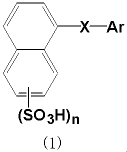
nは、ナフタレン環に結合するスルホン基数を表し、1~4を満たす整数であるが、当該化合物に高電子受容性および高溶解性を付与することを考慮すると、n=1または2が好ましい。
中でも、下記式(2)で示される化合物が、好適である。

ここで、アリール基としては、フェニル基、キシリル基、トリル基、ビフェニル基、ナフチル基等のアリール基が挙げられ、これらのアリール基は置換基を有していてもよい。
この置換基としては、水酸基、アミノ基、シラノール基、チオール基、カルボキシル基、リン酸基、リン酸エステル基、エステル基、チオエステル基、アミド基、ニトロ基、シアノ基、一価炭化水素基、オルガノオキシ基、オルガノアミノ基、オルガノシリル基、オルガノチオ基、アシル基、スルホン基、ハロゲン原子等が挙げられるが、これらに限定されるものではない。
オルガノアミノ基の具体例としては、メチルアミノ基、エチルアミノ基、プロピルアミノ基、ブチルアミノ基、ペンチルアミノ基、ヘキシルアミノ基、ヘプチルアミノ基、オクチルアミノ基、ノニルアミノ基、デシルアミノ基、ラウリルアミノ基等のアルキルアミノ基;ジメチルアミノ基、ジエチルアミノ基、ジプロピルアミノ基、ジブチルアミノ基、ジペンチルアミノ基、ジヘキシルアミノ基、ジヘプチルアミノ基、ジオクチルアミノ基、ジノニルアミノ基、ジデシルアミノ基等のジアルキルアミノ基;シクロヘキシルアミノ基等のジシクロアルキルアミノ基;モルホリノ基などが挙げられる。
オルガノチオ基の具体例としては、メチルチオ基、エチルチオ基、プロピルチオ基、ブチルチオ基、ペンチルチオ基、ヘキシルチオ基、ヘプチルチオ基、オクチルチオ基、ノニルチオ基、デシルチオ基、ラウリルチオ基などのアルキルチオ基が挙げられる。
ハロゲン原子としては、フッ素、塩素、臭素、ヨウ素原子が挙げられる
上記一価炭化水素基、オルガノオキシ基、オルガノアミノ基、オルガノアミノ基、オルガノシリル基、オルガノチオ基、アシル基の炭素数は、特に限定されるものではないが、一般に炭素数1~20、好ましくは1~8である。
上述の各置換基の中でも、フッ素原子、スルホン基、シアノ基、オルガノオキシ基、アルキル基、オルガノシリル基がより好ましい。
なお、以上の置換基において、置換基同士が連結されて環状である部分を含んでいてもよい。
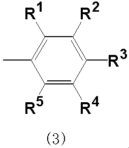
ハロゲン原子としては、塩素、臭素、フッ素、ヨウ素原子のいずれでもよいが、本発明においては、特にフッ素原子が好適である。
炭素数1~10のアルキル基としては、メチル基、エチル基、n-プロピル基、i-プロピル基、n-ブチル基、i-ブチル基、t-ブチル基、n-ペンチル基、n-ヘキシル基、n-ヘプチル基、n-オクチル基、n-ノニル基、2-エチルヘキシル基、n-デシル基、シクロペンチル基、シクロヘキシル基等が挙げられる。
炭素数2~10のハロゲン化アルケニル基としては、パーフルオロビニル基、パーフルオロプロペニル基(アリル基)、パーフルオロブテニル基等が挙げられる。

例えば、下記式(5)で示されるナフタレンスルホン酸化合物のXH基に対し、上述のアリール基を与える試薬を作用させて得ることができる。反応の方法は、特に限定されるものではなく、例えば、一般的な求核置換反応を用いることができる。

触媒としては、例えば、リチウム、カリウム、水素化リチウム、水素化ナトリウム、t-ブトキシリチウム、t-ブトキシナトリウム、t-ブトキシカリウム、リチウム-ジイソプロピルアミド、n-ブチルリチウム、s-ブチルリチウム、t-ブチルリチウム、リチウムヘキサメチルジシラジド、ナトリウムヘキサメチルジシラジド、カリウムヘキサメチルジシラジド、水酸化リチウム、水酸化ナトリウム、水酸化カリウム、水酸化バリウム、酸化バリウム、炭酸リチウム、炭酸ナトリウム、炭酸カリウム、炭酸セシウム、炭酸カルシウム、炭酸水素ナトリウム、トリエチルアミン、ジイソプロピルエチルアミン、テトラメチルエチレンジアミン、トリエチレンジアミン、ピリジン、ジメチルアミノピリジン、イミダゾール等の塩基;塩酸、硫酸、五酸化二リン、塩化アルミニウム(III)、三フッ化ホウ素ジエチルエーテル錯体、二塩化エチルアルミニウム、塩化ジエチルアルミニウム等の脱水縮合剤などを用いることができ、中でも、水素化ナトリウム、炭酸ナトリウム、炭酸カリウムを用いることが好適である。これらの触媒の使用量は特に制限はないが、式(5)の化合物に対して1.0~1.5倍モル用いることが好ましい。
反応温度は、通常、-50℃から使用する溶媒の沸点まで可能であるが、0~140℃の範囲が好ましい。反応時間は、通常、0.1~100時間である。
反応終了後、反応溶媒の留去、陽イオン交換樹脂によるスルホン酸塩のプロトン化、メタノール等の溶媒による抽出操作、再沈殿操作等により、精製することができる。
本発明において、電荷輸送性ワニスとは、電荷輸送機構の本体である電荷輸送性物質と、上記式(1)で表される電子受容性物質との少なくとも2種の物質を溶剤中に含有するものである。電子受容性物質は、電荷輸送能および成膜均一性を向上させるために用いられるものであり、電荷受容性ドーパント物質と同義である。
本発明の電荷輸送性ワニスにおいて、これらの物質は、溶剤によって完全に溶解していてもよく、均一に分散していてもよい。
また、電荷輸送性とは、導電性と同義であり、本発明においては正孔輸送性と同義である。電荷輸送性ワニスは、そのもの自体に電荷輸送性があってもよく、ワニスから得られる固体膜に電荷輸送性があってもよい。
ここで、ハロゲン原子、一価炭化水素基、オルガノオキシ基、オルガノアミノ基、オルガノシリル基、オルガノチオ基、およびアシル基の具体例としては、上述と同様のものが挙げられる。
好ましい置換基として、フッ素原子、スルホン基、置換もしくは非置換のオルガノオキシ基、アルキル基、オルガノシリル基が挙げられる。なお、共役単位が連結して形成される共役鎖は、環状である部分を含んでいてもよい。


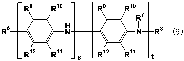
さらに、R6が水素原子、かつ、R8がフェニル基である場合、すなわち、式(9)のオリゴアニリン誘導体の両末端がフェニル基で封止されていることが好ましい。
これらの電荷輸送物質は1種類のみを使用してもよく、また2種類以上の物質を組み合わせて使用してもよい。
高溶解性溶剤としては、特に限定されるものではなく、例えば、水、メタノール、N,N-ジメチルホルムアミド、N,N-ジメチルアセトアミド、N-メチルピロリドン、1,3-ジメチル-2-イミダゾリジノン、ジメチルスルホキシド、クロロホルム、トルエン、メタノール等が挙げられる。
高粘度有機溶剤としては、特に限定されるものではなく、例えば、シクロヘキサノール、エチレングリコール、エチレングリコールジクリシジルエーテル、1,3-オクチレングリコール、ジエチレングリコール、ジプロピレングリコール、トリエチレングリコール、トリプロピレングリコール、1,3-ブタンジオール、1,4-ブタンジオール、プロピレングリコール、へキシレングリコール等が挙げられる。
このような溶剤としては、特に限定されるものではなく、例えば、ブチルセロソルブ、ジエチレングリコールジエチルエーテル、ジプロピレングリコールモノメチルエーテル、エチルカルビトール、ジアセトンアルコール、γ-ブチロラクトン、乳酸エチル等が挙げられる。
ワニスの塗布方法としては、特に限定されるものではないが、ディップ法、スピンコート法、スプレー法、インクジェット法、転写印刷法、ロールコート法、刷毛塗り等が挙げられ、いずれにおいても均一な成膜が可能である。
焼成温度は、溶剤を蒸発させることができれば特に限定されないが、40~250℃が好ましい。より高い均一成膜性を発現させるため、また基材上で反応を進行させるために、2段階以上の温度変化をつけてもよい。
使用する電極基板は、洗剤、アルコール、純水等による液体洗浄を行って予め浄化しておき、陽極基板では、使用直前にオゾン処理、酸素-プラズマ処理等の表面処理を行うことが好ましい。ただし陽極材料が有機物を主成分とする場合、表面処理は行わなくともよい。
すなわち、陽極基板に対して当該正孔輸送性ワニスを用いて上記の膜作製方法により、電極上に正孔輸送性薄膜を作製する。これを真空蒸着装置内に導入し、正孔輸送層、発光層、電子輸送層、電子注入層、陰極金属を順次蒸着してOLED素子とする。この際、発光領域をコントロールするために任意の層間にキャリアブロック層を設けてもよい。
正孔輸送層を形成する材料としては、(トリフェニルアミン)ダイマー誘導体(TPD)、(α-ナフチルジフェニルアミン)ダイマー(α-NPD)、[(トリフェニルアミン)ダイマー]スピロダイマー(Spiro-TAD)等のトリアリールアミン類、4,4’,4”-トリス[3-メチルフェニル(フェニル)アミノ]トリフェニルアミン(m-MTDATA)、4,4’,4”-トリス[1-ナフチル(フェニル)アミノ]トリフェニルアミン(1-TNATA)等のスターバーストアミン類、5,5”-ビス-{4-[ビス(4-メチルフェニル)アミノ]フェニル}-2,2’:5’,2”-ターチオフェン(BMA-3T)等のオリゴチオフェン類を挙げることができる。
発光層を形成する材料としては、トリス(8-キノリノラート)アルミニウム(III)(Alq3)、ビス(8-キノリノラート)亜鉛(II)(Znq2)、ビス(2-メチル-8-キノリノラート)(p-フェニルフェノラート)アルミニウム(III)(BAlq)、4,4’-ビス(2,2-ジフェニルビニル)ビフェニル(DPVBi)等が挙げられる。なお、電子輸送材料または正孔輸送材料と、発光性ドーパントとを共蒸着することによって発光層を形成してもよい。
発光性ドーパントとしては、キナクリドン、ルブレン、クマリン540、4-(ジシアノメチレン)-2-メチル-6-(p-ジメチルアミノスチリル)-4H-ピラン(DCM)、トリス(2-フェニルピリジン)イリジウム(III)(Ir(ppy)3)、(1,10-フェナントロリン)-トリス(4,4,4-トリフルオロ-1-(2-チエニル)-ブタン-1,3-ジオナート)ユーロピウム(III)(Eu(TTA)3phen)等が挙げられる。
キャリアブロック層を形成する材料としては、PBD、TAZ、およびBCPが挙げられる。
陰極材料としては、アルミニウム、マグネシウム-銀合金、アルミニウム-リチウム合金、リチウム、ナトリウム、カリウム、セシウム等が挙げられる。
陰極基板上に当該電子輸送性ワニスを用いて電子輸送性薄膜を作製し、これを真空蒸着装置内に導入し、上記と同様の材料を用いて電子輸送層、発光層、正孔輸送層、正孔注入層を形成した後、陽極材料をスパッタリング等の方法により成膜してOLED素子とする。
上記OLED素子作製において、正孔輸送層、発光層、電子輸送層、電子注入層の真空蒸着操作を行う代わりに、発光性電荷輸送性高分子層を形成することにより、本発明の電荷輸送性ワニスによって形成される電荷輸送性薄膜を含むPLED素子を作製することができる。
具体的には、陽極基板に対して当該正孔輸送性ワニスを上記の方法により塗布して電極上に正孔輸送性薄膜を作製し、その上部に発光性電荷輸送性高分子層を形成し、さらに、陰極電極を蒸着してPLED素子とする。
あるいは、陰極基板に対して当該電子輸送性ワニスを用い、上記の方法により電極上に電子輸送性薄膜を作製し、その上部に発光性電荷輸送性高分子層を形成し、さらに陽極電極をスパッタリング、蒸着、スピンコート等で作製してPLED素子とする。
発光性電荷輸送性高分子層の形成法としては、発光性電荷輸送性高分子材料、またはこれに発光性ドーパントを加えた材料に対して溶剤を加え、溶解または均一に分散させ、正孔輸送性薄膜を形成した電極基板に塗布した後に、溶剤の蒸発により成膜する方法が挙げられる。
発光性電荷輸送性高分子材料としては、ポリ(9,9-ジアルキルフルオレン)(PDAF)等のポリフルオレン誘導体、ポリ(2-メトキシ-5-(2’-エチルヘキソキシ)-1,4-フェニレンビニレン)(MEH-PPV)等のポリフェニレンビニレン誘導体、ポリ(3-アルキルチオフェン)(PAT)などのポリチオフェン誘導体、ポリビニルカルバゾール(PVCz)等を挙げることができる。
塗布方法としては、特に限定されるものではないが、ディップ法、スピンコート法、転写印刷法、ロールコート法、刷毛塗り等が挙げられる。塗布は、窒素、アルゴン等の不活性ガス下で行うことが望ましい。
溶剤の蒸発法としては不活性ガス下または真空中で、オーブンまたはホットプレートで加熱する方法を挙げることができる。

p-フェニレンジアミン12.977gを、トルエン2リットルに溶解し、これに脱水縮合剤であるテトラ-n-ブトキシチタン245.05gを加え、70℃で30分間溶解した。その後、p-ヒドロキシジフェニルアミン53.346gを添加し、窒素雰囲気下、反応温度100℃で24時間反応させた。反応終了後、反応液を濾過し、濾物をトルエン、エーテルで順次洗浄した後、乾燥して銀色結晶を得た。得られた結晶に対して25質量部のジオキサン、0.2当量のヒドラジン一水和物を加え、反応系内を窒素置換した後、加熱還流して結晶を溶解した。得られた溶液に、トルエンを結晶に対して25質量部加えて溶液を懸濁し、加熱還流後、さらにジオキサンを10質量部加えて加熱還流して溶解し、得られた溶液を熱時濾過した。
濾液から析出した固体を再結晶し、窒素雰囲気下、トルエン-ジオキサン(1:1)、エーテルで順次洗浄した後に濾取し、得られた結晶を減圧下、60℃で10時間乾燥した。同様の再結晶操作をもう一度繰り返して白色結晶39.60gを得た(収率75%)。
下記反応式に従い、パーフルオロトルエンナフタレンスルホン酸化合物(以下、7FNS-1と略す)を合成した。

5時間後、炭酸カリウムを除去するために濾過を行った。得られた濾液を、減圧下、濃縮乾固した。残渣にメタノール50mlを加え、30分間洗浄を行った後、懸濁液を濾過した。得られた濾物を減圧下で乾固した後、純水500mlを加え溶解し、陽イオン交換樹脂ダウエックス650C(Hタイプ約200ml、留出溶媒:水)を用いたカラムクロマトグラフィーにより精製した。
pH1以下の分画を減圧下で濃縮乾固し、白色粉末12.1gを得た(収率81%)。
分子量;520.35
MALDI-TOF;519.0[M-H]-
下記反応式に従い、パーフルオロアリルベンゼンナフタレンスルホン酸化合物(以下、9FNS-1と略す)を合成した。

分子量;582.37
MALDI-TOF;581.0[M-H]-
下記反応式に従い、ジシアノパーフルオロトルエンスルホン酸化合物(以下、3FNS-1と略す)を合成した。
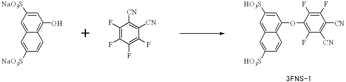
2時間後、析出している反応物を溶解させるため50mlのDMFを加えた。次に、炭酸カリウムを除去するために濾過を行った。得られた濾液を200mlのIPAに滴下し、再沈殿を行った。濾過して得られた濾物を減圧下で乾固した後、純水50mlを加えて溶解し、陽イオン交換樹脂ダウエックス650C(Hタイプ約100ml、留出溶媒:水)を用いたカラムクロマトグラフィーにより精製した。
pH1以下の分画を減圧下で濃縮乾固し、白色粉末5.31gを得た(収率97%)
分子量;484.38
LC-MS;482.96[M-H]-
下記反応式に従い、シアノパーフルオロトルエンスルホン酸化合物(以下、4FNS-2と略す)を合成した。
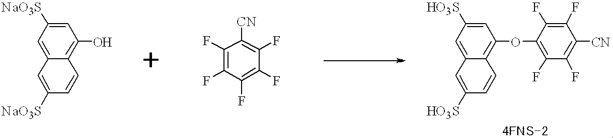
分子量;477.36
LC-MS;475.95[M-H]-
下記反応式に従い、ナフタレンジスルホン酸化合物(以下、NSO-2と略す)を合成した。

よく乾燥させた1-ナフトール-3,6-ジスルホン酸ナトリウム(東京化成工業(株)製)934mgに、窒素雰囲気下で、パーフルオロビフェニル450mg、60%水素化ナトリウム166mg、および無水N,N-ジメチルイミダゾリジノン50mlを順次加え、反応系を窒素置換した後、80℃で43時間撹拌した。
室温まで放冷後、水を加えて反応を停止させ、減圧下、濃縮乾固した。残渣にメタノール5mlを加え、得られた懸濁液をジエチルエーテル100mlに撹拌しながら加えた。室温で1時間撹拌後、析出した固体を濾取し、濾物にメタノール25mlを加え超音波で懸濁させた。不溶の固体を濾過によって除去し、濾液を減圧下濃縮乾固した。残渣にメタノール-水(1:2)12mlを加え溶解し、陽イオン交換樹脂ダウエックス650C(Hタイプ約40ml、留出溶媒:メタノール-水(1:2))を用いたカラムクロマトグラフィーにより精製した。
pH1以下の分画を減圧下で濃縮乾固し、イソプロパノールで一回共沸した後、残渣にイソプロパノール2mlを加え、得られた溶液をジエチルエーテル50ml中に撹拌しながら加えた。室温で1時間撹拌後、上澄み液を除去し、残渣を減圧下で乾固して黄色粉末984mgを得た(収率81%)。
上記実施例1~4および比較例1で得られた各アリールスルホン酸化合物について、下記手法により溶媒への溶解性試験を行った。結果を表1に示す。
[実施例5~8]
実施例1~4で得られた各アリールスルホン酸化合物と、これに対して0.5モル当量のPTAとを、1,3-ジメチル-2-イミダゾリジノン(以下、DMIと略す)1gに固形分7.0質量%となるように溶解させてワニスを調製した。
得られたワニスに、シクロヘキサノール(以下、CHAと略す)を加えていき、ワニスが白濁したときのCHA量を溶解性の指標とした。
比較例1で得られたNSO-2と、これに対して1.0モル当量のPTAとを、DMI1gに固形分7.0質量%となるように溶解させてワニスを調製した。
得られたワニスに、CHAを加えていき、ワニスが白濁したときのCHA量を溶解性の指標とした。

[比較例3]
合成例1で得られたPTAと、これに対して1.0モル当量の比較例1で得られたNSO-2とを、DMI:CHA:プロピレングリコール(以下PGと略す)=2:3:1(質量比)の割合の溶媒に、固形分2.8質量%になるように溶解させてワニスを調製した。
このワニスを用いてITOガラス基板上へスピンコート法により約30nmの均一な薄膜を作製した後、真空蒸着装置内に導入し、α-NPD、Alq3、LiF、Alを順次蒸着し、OLED素子を得た。膜厚はそれぞれ、30nm、50nm、1nm、120nmとし、それぞれ8×10⁻⁴Pa以下の圧力となってから蒸着操作を行い、蒸着レートはLiFを除いて、0.3~0.4nm/sとし、LiFについては、0.02~0.04nm/sとした。蒸着操作間の移動操作は真空中で行った。
合成例1で得られたPTAと、これに対して2.0モル当量の実施例1で得られた7FNS-1とを、DMI:CHA:PG=2:3:1(質量比)の割合の溶媒に、固形分2.8質量%になるように溶解させてワニスを調製した。
このワニスを用い、比較例3と同様にして薄膜を作製した後、比較例3と同様にして蒸着操作を行い、OLED素子を得た。
1.0モル当量の実施例1で得られた7FNS-1を用いた以外は、実施例9と同様にして、OLED素子を得た。
3.0モル当量の実施例1で得られた7FNS-1を用いた以外は、実施例9と同様にして、OLED素子を得た。
合成例1で得られたPTAと、これに対して2.0モル当量の実施例2で得られた9FNS-1とを、DMI:CHA:PG=2:3:1(質量比)の割合の溶媒に、固形分2.8質量%になるように溶解させてワニスを調製した。
このワニスを用い、比較例3と同様にして薄膜を作製した後、比較例3と同様にして蒸着操作を行い、OLED素子を得た。
1.0モル当量の実施例2で得られた9FNS-1を用いた以外は、実施例12と同様にして、OLED素子を得た。
3.0モル当量の実施例2で得られた9FNS-1を用いた以外は、実施例12と同様にして、OLED素子を得た。
2.0モル当量の実施例4で得られた4FNS-2を用いた以外は、実施例12と同様にして、OLED素子を得た。
なお、OLED素子の特性は、有機EL発光効率測定装置(EL1003、プレサイスゲージ製)を使用して測定した。
図3,4に示されるように、実施例12で作製したOLED素子は、比較例3の素子と比べて電圧-輝度、電圧-電流密度において特に優れていることがわかる。また、実施例13,14では、電圧が10V以下の領域において、比較例3よりも輝度、電流密度が優れていることがわかる。
図5,6に示されるように実施例15で作製したOLED素子は、比較例3の素子と同等以上の性質を有していることがわかる。
Claims (8)
- 式(1)で表されることを特徴とするアリールスルホン酸化合物。

- 式(2)で表される請求項1記載のアリールスルホン酸化合物。
- 前記Arが、下記式(3)で示される請求項1または2記載のアリールスルホン酸化合物。

- 前記Arが、下記式(4)で示される請求項3記載のアリールスルホン酸化合物。

- 請求項1~4のいずれか1項記載のアリールスルホン酸化合物からなる電子受容性物質。
- 請求項5記載の電子受容性物質、電荷輸送性物質、および溶剤を含む電荷輸送性ワニス。
- 請求項5記載の電子受容性物質、および電荷輸送性物質を含む電荷輸送性薄膜。
- 請求項7記載の電荷輸送性薄膜を有する有機エレクトロルミネッセンス素子。
Priority Applications (6)
| Application Number | Priority Date | Filing Date | Title |
|---|---|---|---|
| EP09706250.9A EP2246325B1 (en) | 2008-01-29 | 2009-01-26 | Arylsulfonic acid compound and use thereof as electron-acceptor material |
| KR20107018640A KR101484740B1 (ko) | 2008-01-29 | 2009-01-26 | 아릴술폰산 화합물 및 전자수용성 물질로서의 이용 |
| US12/864,914 US8460582B2 (en) | 2008-01-29 | 2009-01-26 | Arylsulfonic acid compound and use thereof as electron-acceptor material |
| CN2009801081925A CN101959852B (zh) | 2008-01-29 | 2009-01-26 | 芳基磺酸化合物及其作为电子受体材料的应用 |
| JP2009551506A JP5407872B2 (ja) | 2008-01-29 | 2009-01-26 | アリールスルホン酸化合物および電子受容性物質としての利用 |
| US13/891,244 US9082985B2 (en) | 2008-01-29 | 2013-05-10 | Arylsulfonic acid compound and use thereof as electron-acceptor material |
Applications Claiming Priority (2)
| Application Number | Priority Date | Filing Date | Title |
|---|---|---|---|
| JP2008-017139 | 2008-01-29 | ||
| JP2008017139 | 2008-01-29 |
Related Child Applications (2)
| Application Number | Title | Priority Date | Filing Date |
|---|---|---|---|
| US12/864,914 A-371-Of-International US8460582B2 (en) | 2008-01-29 | 2009-01-26 | Arylsulfonic acid compound and use thereof as electron-acceptor material |
| US13/891,244 Continuation US9082985B2 (en) | 2008-01-29 | 2013-05-10 | Arylsulfonic acid compound and use thereof as electron-acceptor material |
Publications (1)
| Publication Number | Publication Date |
|---|---|
| WO2009096352A1 true WO2009096352A1 (ja) | 2009-08-06 |
Family
ID=40912705
Family Applications (1)
| Application Number | Title | Priority Date | Filing Date |
|---|---|---|---|
| PCT/JP2009/051169 Ceased WO2009096352A1 (ja) | 2008-01-29 | 2009-01-26 | アリールスルホン酸化合物および電子受容性物質としての利用 |
Country Status (7)
| Country | Link |
|---|---|
| US (2) | US8460582B2 (ja) |
| EP (2) | EP2620427B1 (ja) |
| JP (1) | JP5407872B2 (ja) |
| KR (1) | KR101484740B1 (ja) |
| CN (1) | CN101959852B (ja) |
| TW (1) | TWI447099B (ja) |
| WO (1) | WO2009096352A1 (ja) |
Cited By (21)
| Publication number | Priority date | Publication date | Assignee | Title |
|---|---|---|---|---|
| US8252829B2 (en) | 2009-06-05 | 2012-08-28 | Link Medicine Corporation | Aminopyrrolidinone derivatives and uses thereof |
| WO2013129249A1 (ja) | 2012-03-02 | 2013-09-06 | 日産化学工業株式会社 | 電荷輸送性ワニス |
| JP5413369B2 (ja) * | 2008-10-09 | 2014-02-12 | 日産化学工業株式会社 | 電荷輸送性ワニス |
| WO2014188998A1 (ja) | 2013-05-20 | 2014-11-27 | 日産化学工業株式会社 | トリフェニルアミン誘導体およびその利用 |
| WO2014203882A1 (ja) | 2013-06-21 | 2014-12-24 | 日産化学工業株式会社 | アニリン誘導体、電荷輸送性ワニス及び有機エレクトロルミネッセンス素子 |
| WO2015050253A1 (ja) | 2013-10-04 | 2015-04-09 | 日産化学工業株式会社 | アニリン誘導体およびその利用 |
| WO2015053320A1 (ja) | 2013-10-09 | 2015-04-16 | 日産化学工業株式会社 | アリールスルホン酸化合物及びその利用並びにアリールスルホン酸化合物の製造方法 |
| WO2015111654A1 (ja) | 2014-01-27 | 2015-07-30 | 日産化学工業株式会社 | アリールスルホン酸化合物及びその利用 |
| WO2015115515A1 (ja) * | 2014-01-31 | 2015-08-06 | 日産化学工業株式会社 | アリールスルホン酸化合物及びその利用 |
| WO2016006673A1 (ja) * | 2014-07-11 | 2016-01-14 | 日産化学工業株式会社 | 電荷輸送性ワニス |
| EP3024049A1 (en) | 2014-11-18 | 2016-05-25 | Heraeus Deutschland GmbH & Co. KG | Fluorinated aromatic small molecules as functional additives for dispersion of conductive polymers |
| WO2017150412A1 (ja) | 2016-03-03 | 2017-09-08 | 日産化学工業株式会社 | 電荷輸送性ワニス |
| WO2017164158A1 (ja) | 2016-03-24 | 2017-09-28 | 日産化学工業株式会社 | アリールアミン誘導体とその利用 |
| WO2018147204A1 (ja) | 2017-02-07 | 2018-08-16 | 日産化学工業株式会社 | 電荷輸送性ワニス |
| WO2018186340A1 (ja) | 2017-04-05 | 2018-10-11 | 日産化学株式会社 | 電荷輸送性ワニス |
| WO2018216507A1 (ja) * | 2017-05-25 | 2018-11-29 | 日産化学株式会社 | 電荷輸送性薄膜の製造方法 |
| WO2019124412A1 (ja) | 2017-12-20 | 2019-06-27 | 日産化学株式会社 | スルホン酸エステル化合物及びその利用 |
| WO2020066979A1 (ja) | 2018-09-25 | 2020-04-02 | 日産化学株式会社 | 有機機能膜付き基板の製造方法 |
| WO2020218316A1 (ja) | 2019-04-26 | 2020-10-29 | 日産化学株式会社 | アリールスルホン酸エステル化合物の製造方法 |
| KR20240036640A (ko) | 2021-07-26 | 2024-03-20 | 닛산 가가쿠 가부시키가이샤 | 불소화아릴술폰산 폴리머 화합물 및 그 이용 |
| KR20240163623A (ko) | 2022-03-28 | 2024-11-19 | 닛산 가가쿠 가부시키가이샤 | 폴리머 및 그 이용 |
Families Citing this family (3)
| Publication number | Priority date | Publication date | Assignee | Title |
|---|---|---|---|---|
| EP4109573A1 (en) * | 2015-03-17 | 2022-12-28 | Nissan Chemical Corporation | Photosensor element |
| KR102138411B1 (ko) * | 2017-07-07 | 2020-07-27 | 주식회사 엘지화학 | 화합물을 포함하는 코팅 조성물 및 이를 포함하는 유기 발광 소자 |
| KR102720709B1 (ko) * | 2018-11-29 | 2024-10-22 | 주식회사 엘지화학 | 신규한 화합물 및 이를 포함하는 유기발광 소자 |
Citations (4)
| Publication number | Priority date | Publication date | Assignee | Title |
|---|---|---|---|---|
| JPH0267262A (ja) * | 1988-07-09 | 1990-03-07 | Bayer Ag | 硫黄を経て結合した置換基をもつ(ヘテロ)アリールオキシナフタレン |
| JPH09158091A (ja) * | 1995-12-13 | 1997-06-17 | Nippon Kayaku Co Ltd | 紙、パルプの蛍光増白法 |
| JP2002151272A (ja) | 2000-11-09 | 2002-05-24 | Nissan Chem Ind Ltd | 電界発光素子 |
| WO2006025342A1 (ja) | 2004-08-31 | 2006-03-09 | Nissan Chemical Industries, Ltd. | アリールスルホン酸化合物及び電子受容性物質としての利用 |
Family Cites Families (3)
| Publication number | Priority date | Publication date | Assignee | Title |
|---|---|---|---|---|
| US6218571B1 (en) * | 1999-10-27 | 2001-04-17 | Lifescan, Inc. | 8-(anilino)-1-naphthalenesulfonate analogs |
| US6998068B2 (en) * | 2003-08-15 | 2006-02-14 | 3M Innovative Properties Company | Acene-thiophene semiconductors |
| CN102227830B (zh) * | 2008-10-09 | 2015-02-18 | 日产化学工业株式会社 | 电荷传输性清漆 |
-
2009
- 2009-01-23 TW TW098103147A patent/TWI447099B/zh active
- 2009-01-26 JP JP2009551506A patent/JP5407872B2/ja active Active
- 2009-01-26 CN CN2009801081925A patent/CN101959852B/zh active Active
- 2009-01-26 EP EP13165339.6A patent/EP2620427B1/en not_active Ceased
- 2009-01-26 EP EP09706250.9A patent/EP2246325B1/en not_active Not-in-force
- 2009-01-26 WO PCT/JP2009/051169 patent/WO2009096352A1/ja not_active Ceased
- 2009-01-26 US US12/864,914 patent/US8460582B2/en not_active Expired - Fee Related
- 2009-01-26 KR KR20107018640A patent/KR101484740B1/ko active Active
-
2013
- 2013-05-10 US US13/891,244 patent/US9082985B2/en not_active Expired - Fee Related
Patent Citations (4)
| Publication number | Priority date | Publication date | Assignee | Title |
|---|---|---|---|---|
| JPH0267262A (ja) * | 1988-07-09 | 1990-03-07 | Bayer Ag | 硫黄を経て結合した置換基をもつ(ヘテロ)アリールオキシナフタレン |
| JPH09158091A (ja) * | 1995-12-13 | 1997-06-17 | Nippon Kayaku Co Ltd | 紙、パルプの蛍光増白法 |
| JP2002151272A (ja) | 2000-11-09 | 2002-05-24 | Nissan Chem Ind Ltd | 電界発光素子 |
| WO2006025342A1 (ja) | 2004-08-31 | 2006-03-09 | Nissan Chemical Industries, Ltd. | アリールスルホン酸化合物及び電子受容性物質としての利用 |
Non-Patent Citations (17)
| Title |
|---|
| APPLIED PHYSICS LETTERS, U.S.A., vol. 51, 1987, pages 913 - 915 |
| APPLIED PHYSICS LETTERS, U.S.A., vol. 64, 1994, pages 1245 - 1247 |
| APPLIED PHYSICS LETTERS, U.S.A., vol. 69, 1996, pages 2160 - 2162 |
| APPLIED PHYSICS LETTERS, U.S.A., vol. 70, 1997, pages 152 - 154 |
| APPLIED PHYSICS LETTERS, U.S.A., vol. 72, 1998, pages 2660 - 2662 |
| BULLETIN OF CHEMICAL SOCIETY OF JAPAN, vol. 67, 1994, pages 1749 - 1752 |
| HETEROCYCLES, vol. 26, 1987, pages 1793 - 1796 |
| HETEROCYCLES, vol. 26, 1987, pages 939 - 942 |
| IEEE TRANSACTIONS ON ELECTRON DEVICES, U.S.A., vol. 44, 1997, pages 1245 - 1248 |
| JAPANESE JOURNAL OF APPLIED PHYSICS, vol. 38, 1999, pages L1348 - 1350 |
| KOSOWER, E. M. ET AL.: "Intramolecular donor-acceptor systems. 10. Multiple fluorescences from 8-(N-phenylamino)-1- naphthalenesulfonates", JOURNAL OF THE AMERICAN CHEMICAL SOCIETY, vol. 105, no. 20, 1983, pages 6236 - 6243, XP008138550 * |
| NATURE, THE UK, vol. 347, 1990, pages 539 - 541 |
| NATURE, THE UK, vol. 357, 1992, pages 477 - 479 |
| NATURE, THE UNITED KINGDOM, vol. 347, 1990, pages 539 - 541 |
| NATURE, THE UNITED KINGDOM, vol. 357, 1992, pages 477 - 479 |
| See also references of EP2246325A4 |
| SYNTHETIC METALS, THE U.S.A., vol. 84, 1997, pages 119 - 120 |
Cited By (40)
| Publication number | Priority date | Publication date | Assignee | Title |
|---|---|---|---|---|
| JP5413369B2 (ja) * | 2008-10-09 | 2014-02-12 | 日産化学工業株式会社 | 電荷輸送性ワニス |
| US8252829B2 (en) | 2009-06-05 | 2012-08-28 | Link Medicine Corporation | Aminopyrrolidinone derivatives and uses thereof |
| WO2013129249A1 (ja) | 2012-03-02 | 2013-09-06 | 日産化学工業株式会社 | 電荷輸送性ワニス |
| US10233337B2 (en) | 2012-03-02 | 2019-03-19 | Nissan Chemical Industries, Ltd. | Charge-transporting varnish |
| WO2014188998A1 (ja) | 2013-05-20 | 2014-11-27 | 日産化学工業株式会社 | トリフェニルアミン誘導体およびその利用 |
| WO2014203882A1 (ja) | 2013-06-21 | 2014-12-24 | 日産化学工業株式会社 | アニリン誘導体、電荷輸送性ワニス及び有機エレクトロルミネッセンス素子 |
| WO2015050253A1 (ja) | 2013-10-04 | 2015-04-09 | 日産化学工業株式会社 | アニリン誘導体およびその利用 |
| JPWO2015053320A1 (ja) * | 2013-10-09 | 2017-03-09 | 日産化学工業株式会社 | アリールスルホン酸化合物及びその利用並びにアリールスルホン酸化合物の製造方法 |
| WO2015053320A1 (ja) | 2013-10-09 | 2015-04-16 | 日産化学工業株式会社 | アリールスルホン酸化合物及びその利用並びにアリールスルホン酸化合物の製造方法 |
| US10177315B2 (en) | 2013-10-09 | 2019-01-08 | Nissan Chemical Industries, Ltd. | Arylsulfonic acid compound, use thereof, and method for producing arylsulfonic acid compound |
| KR102257239B1 (ko) | 2013-10-09 | 2021-05-27 | 닛산 가가쿠 가부시키가이샤 | 아릴설폰산 화합물 및 그 이용 그리고 아릴설폰산 화합물의 제조 방법 |
| KR20160067924A (ko) | 2013-10-09 | 2016-06-14 | 닛산 가가쿠 고교 가부시키 가이샤 | 아릴설폰산 화합물 및 그 이용 그리고 아릴설폰산 화합물의 제조 방법 |
| KR20160113637A (ko) | 2014-01-27 | 2016-09-30 | 닛산 가가쿠 고교 가부시키 가이샤 | 아릴설폰산 화합물 및 그 이용 |
| JPWO2015111654A1 (ja) * | 2014-01-27 | 2017-03-23 | 日産化学工業株式会社 | アリールスルホン酸化合物及びその利用 |
| WO2015111654A1 (ja) | 2014-01-27 | 2015-07-30 | 日産化学工業株式会社 | アリールスルホン酸化合物及びその利用 |
| EP3101003A4 (en) * | 2014-01-31 | 2017-09-13 | Nissan Chemical Industries, Ltd. | Aryl sulfonic acid compound and use thereof |
| JPWO2015115515A1 (ja) * | 2014-01-31 | 2017-03-23 | 日産化学工業株式会社 | アリールスルホン酸化合物及びその利用 |
| KR20160114629A (ko) * | 2014-01-31 | 2016-10-05 | 닛산 가가쿠 고교 가부시키 가이샤 | 아릴설폰산 화합물 및 그 이용 |
| KR102255160B1 (ko) | 2014-01-31 | 2021-05-24 | 닛산 가가쿠 가부시키가이샤 | 아릴설폰산 화합물 및 그 이용 |
| TWI643841B (zh) * | 2014-01-31 | 2018-12-11 | 日商日產化學工業股份有限公司 | Arylsulfonic acid compounds and their utilization |
| WO2015115515A1 (ja) * | 2014-01-31 | 2015-08-06 | 日産化学工業株式会社 | アリールスルホン酸化合物及びその利用 |
| JPWO2016006673A1 (ja) * | 2014-07-11 | 2017-04-27 | 日産化学工業株式会社 | 電荷輸送性ワニス |
| WO2016006673A1 (ja) * | 2014-07-11 | 2016-01-14 | 日産化学工業株式会社 | 電荷輸送性ワニス |
| JP2020170876A (ja) * | 2014-07-11 | 2020-10-15 | 日産化学株式会社 | 電荷輸送性ワニス |
| EP3024049A1 (en) | 2014-11-18 | 2016-05-25 | Heraeus Deutschland GmbH & Co. KG | Fluorinated aromatic small molecules as functional additives for dispersion of conductive polymers |
| EP3886194A2 (en) | 2014-11-18 | 2021-09-29 | Heraeus Deutschland GmbH & Co KG | Fluorinated aromatic small molecules as functional additives for dispersion of conductive polymers |
| WO2017150412A1 (ja) | 2016-03-03 | 2017-09-08 | 日産化学工業株式会社 | 電荷輸送性ワニス |
| WO2017164158A1 (ja) | 2016-03-24 | 2017-09-28 | 日産化学工業株式会社 | アリールアミン誘導体とその利用 |
| WO2018147204A1 (ja) | 2017-02-07 | 2018-08-16 | 日産化学工業株式会社 | 電荷輸送性ワニス |
| WO2018186340A1 (ja) | 2017-04-05 | 2018-10-11 | 日産化学株式会社 | 電荷輸送性ワニス |
| JPWO2018216507A1 (ja) * | 2017-05-25 | 2020-03-26 | 日産化学株式会社 | 電荷輸送性薄膜の製造方法 |
| WO2018216507A1 (ja) * | 2017-05-25 | 2018-11-29 | 日産化学株式会社 | 電荷輸送性薄膜の製造方法 |
| KR20200100767A (ko) | 2017-12-20 | 2020-08-26 | 닛산 가가쿠 가부시키가이샤 | 술폰산에스테르 화합물 및 그 이용 |
| WO2019124412A1 (ja) | 2017-12-20 | 2019-06-27 | 日産化学株式会社 | スルホン酸エステル化合物及びその利用 |
| JPWO2019124412A1 (ja) * | 2017-12-20 | 2020-12-24 | 日産化学株式会社 | スルホン酸エステル化合物及びその利用 |
| JP7234937B2 (ja) | 2017-12-20 | 2023-03-08 | 日産化学株式会社 | スルホン酸エステル化合物及びその利用 |
| WO2020066979A1 (ja) | 2018-09-25 | 2020-04-02 | 日産化学株式会社 | 有機機能膜付き基板の製造方法 |
| WO2020218316A1 (ja) | 2019-04-26 | 2020-10-29 | 日産化学株式会社 | アリールスルホン酸エステル化合物の製造方法 |
| KR20240036640A (ko) | 2021-07-26 | 2024-03-20 | 닛산 가가쿠 가부시키가이샤 | 불소화아릴술폰산 폴리머 화합물 및 그 이용 |
| KR20240163623A (ko) | 2022-03-28 | 2024-11-19 | 닛산 가가쿠 가부시키가이샤 | 폴리머 및 그 이용 |
Also Published As
| Publication number | Publication date |
|---|---|
| US9082985B2 (en) | 2015-07-14 |
| EP2246325B1 (en) | 2013-11-06 |
| TWI447099B (zh) | 2014-08-01 |
| EP2620427B1 (en) | 2015-09-23 |
| EP2246325A1 (en) | 2010-11-03 |
| US20100320422A1 (en) | 2010-12-23 |
| US20130240795A1 (en) | 2013-09-19 |
| TW200944494A (en) | 2009-11-01 |
| JP5407872B2 (ja) | 2014-02-05 |
| JPWO2009096352A1 (ja) | 2011-05-26 |
| EP2620427A1 (en) | 2013-07-31 |
| CN101959852A (zh) | 2011-01-26 |
| EP2246325A4 (en) | 2012-01-11 |
| US8460582B2 (en) | 2013-06-11 |
| KR20100119876A (ko) | 2010-11-11 |
| CN101959852B (zh) | 2013-09-18 |
| KR101484740B1 (ko) | 2015-01-20 |
Similar Documents
| Publication | Publication Date | Title |
|---|---|---|
| JP5407872B2 (ja) | アリールスルホン酸化合物および電子受容性物質としての利用 | |
| JP4883297B2 (ja) | アリールスルホン酸化合物及び電子受容性物質としての利用 | |
| JP4596165B2 (ja) | 1,4−ベンゾジオキサンスルホン酸化合物及び電子受容性物質としての利用 | |
| JP4591681B2 (ja) | 電荷輸送性ワニス | |
| JP5446267B2 (ja) | オリゴアニリン化合物およびその利用 | |
| JP5024498B2 (ja) | 電荷輸送性ワニス、電荷輸送性薄膜および有機エレクトロルミネッセンス素子 | |
| JP5196175B2 (ja) | 電荷輸送性ワニス | |
| JP4811573B2 (ja) | 1,4−ジチイン環を有する化合物を含む電荷輸送性有機材料 | |
| JP5136795B2 (ja) | スルホン酸エステル化合物からなる電子受容性物質前駆体およびその利用 |
Legal Events
| Date | Code | Title | Description |
|---|---|---|---|
| WWE | Wipo information: entry into national phase |
Ref document number: 200980108192.5 Country of ref document: CN |
|
| 121 | Ep: the epo has been informed by wipo that ep was designated in this application |
Ref document number: 09706250 Country of ref document: EP Kind code of ref document: A1 |
|
| WWE | Wipo information: entry into national phase |
Ref document number: 2009551506 Country of ref document: JP |
|
| WWE | Wipo information: entry into national phase |
Ref document number: 12864914 Country of ref document: US |
|
| NENP | Non-entry into the national phase |
Ref country code: DE |
|
| WWE | Wipo information: entry into national phase |
Ref document number: 2009706250 Country of ref document: EP |
|
| ENP | Entry into the national phase |
Ref document number: 20107018640 Country of ref document: KR Kind code of ref document: A |