WO2009096376A1 - 電圧電流変換器、それを用いた、微分回路、積分回路およびフィルタ回路並びに電圧電流変換方法 - Google Patents
電圧電流変換器、それを用いた、微分回路、積分回路およびフィルタ回路並びに電圧電流変換方法 Download PDFInfo
- Publication number
- WO2009096376A1 WO2009096376A1 PCT/JP2009/051243 JP2009051243W WO2009096376A1 WO 2009096376 A1 WO2009096376 A1 WO 2009096376A1 JP 2009051243 W JP2009051243 W JP 2009051243W WO 2009096376 A1 WO2009096376 A1 WO 2009096376A1
- Authority
- WO
- WIPO (PCT)
- Prior art keywords
- voltage
- current
- current converter
- converter
- filter
- Prior art date
- Legal status (The legal status is an assumption and is not a legal conclusion. Google has not performed a legal analysis and makes no representation as to the accuracy of the status listed.)
- Ceased
Links
Images






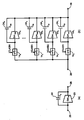
Classifications
-
- G—PHYSICS
- G11—INFORMATION STORAGE
- G11C—STATIC STORES
- G11C27/00—Electric analogue stores, e.g. for storing instantaneous values
- G11C27/02—Sample-and-hold arrangements
- G11C27/024—Sample-and-hold arrangements using a capacitive memory element
-
- G—PHYSICS
- G11—INFORMATION STORAGE
- G11C—STATIC STORES
- G11C27/00—Electric analogue stores, e.g. for storing instantaneous values
- G11C27/02—Sample-and-hold arrangements
-
- H—ELECTRICITY
- H03—ELECTRONIC CIRCUITRY
- H03H—IMPEDANCE NETWORKS, e.g. RESONANT CIRCUITS; RESONATORS
- H03H15/00—Transversal filters
- H03H15/02—Transversal filters using analogue shift registers
- H03H15/023—Transversal filters using analogue shift registers with parallel-input configuration
Definitions
- the present invention relates to a voltage-current conversion technique having a finite impulse response filter characteristic in conversion gain.
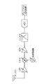
- Fig. 1 shows an example of the configuration of a multimode receiver.
- a low noise amplifier Low Noise Amplifier: LNA
- LNA Low Noise Amplifier
- the mixer circuit down-converts the high frequency signal by integrating the local oscillator output of the same frequency as the high frequency reception signal and the high frequency reception signal amplified by the LNA.
- VGA variable gain amplifier
- the filter sufficiently attenuates interference waves outside the desired signal band.
- An analog-to-digital converter (Analog To Digital Converter: ADC) converts an analog signal that has passed through a filter into a digital signal, and the digital processing circuit performs various signal processing such as demodulation.
- ⁇ Filters built into multimode transceivers are required to have a wide range of variable filter characteristics such as pass bandwidth and order according to the communication standard.
- a discrete time processing filter typified by a switched capacitor filter has attracted attention as a multimode variable filter. Since the bandwidth of the discrete-time processing filter is proportional to the sampling frequency, the bandwidth can be easily changed over a wide range by controlling the sampling frequency.
- the output current of the voltage-current converter is sampled and integrated into the capacitance, so that a finite impulse response (FIR) response (FIR) filter characteristic that is one form of the discrete-time processing filter, Infinite impulse response (Infinite Response IIR) filter characteristics are obtained (Non-Patent Document 1).
- FIR finite impulse response
- IIR Infinite impulse response
- a high-order filter is configured to obtain a steep cut-off characteristic in order to remove an interference wave close to a desired signal (Non-patent Document 2).
- the analog voltage source voltage input from each of a plurality of channels is sampled by a successive approximation type sample-and-hold circuit having a sampling capacitor continuously by switching channels and converted into a digital value.
- the sampling capacitor is initially set by the analog voltage corresponding to the previous conversion result obtained by converting the voltage of the analog voltage source connected to the channel of interest into a digital value.
- the sampling capacitor is charged with the voltage of the analog voltage source connected to the channel of interest, and the current flowing from the analog voltage source to the A / D converter is reduced. Voltage due to output impedance Techniques to minimize the bottom has been disclosed (e.g., see Patent Document 1). JP 2002-176358 A IEEE JSSC Vol.39.No.12, pp.2278-2291, Dec, 2004. IEEE JSSC Vol.35.No.2, pp.212-220, Feb, 2000.
- the present invention has the following features.
- the voltage-current converter of the present invention is a voltage-current converter that converts an input voltage into a current and outputs the current, and has at least one sampling holding unit having a function of sampling and holding the input voltage.
- One or more individual voltage / current converters that output a current corresponding to the voltage held by the sampling holding unit; and a control unit that controls the timing at which the sampling holding unit samples and holds the input voltage; , And outputs a current obtained by adding a part or all of the output current of each individual voltage-current converter.
- the differentiating circuit of the present invention is characterized by having one or more voltage-current converters.
- the integrating circuit of the present invention is characterized by having one or more voltage-current converters.
- the filter circuit of the present invention is characterized by having one or more voltage-current converters.
- the voltage-current conversion method of the present invention also includes a step of sampling and holding the input voltage, and adding a part or all of the output current when outputting a current corresponding to the sampled and held voltage. And converting the frequency characteristic of the conversion gain into a finite impulse response or an infinite impulse response filter characteristic.
- variable filter having a small area and a steep cutoff characteristic can be realized.
- FIG. 4 is a diagram showing a configuration of the voltage-current converter according to the first embodiment of the present invention.
- This voltage-current converter has an input terminal 11, an output terminal 12, an integer “N” or more individual voltage-current converters 131 to 13N (conversion gains are Gm01 to Gm0N, respectively), and a voltage-current converter input.
- N switching elements 141 to 14N connected in series between the terminal 11 and each input terminal of the individual voltage / current converter, and between the individual voltage / current converters 131 to 13N input terminal and a fixed potential.
- N capacitors 151 to 15N and a control unit 16 for controlling the opening and closing of the switching elements 141 to 14N. All the output terminals of the individual voltage / current converters 131 to 13N are connected to the voltage / current converter output terminal 12.
- the open / close elements 141 to 14N and the capacitors 151 to 15N are examples of the sampling holding unit.
- the open / close elements 141 to 14N are all closed when the control clock signal is 1 and open when the control clock signal is 0.
- the control unit 16 generates N-phase control clock signals CLKB1 to CLKBN shown in FIG. 5, and controls the opening and closing of the switching elements 141 to 14N, respectively.
- CLKB1 to CLKBN are clock signals that do not become 1 at the same time and whose rising and falling timings are shifted.
- As a method of obtaining CLKB1 to CLKBN there are a method of generating internally and a method of selecting from a plurality of clock signals supplied from the outside.
- Equation (1) means that the frequency characteristic of the conversion gain of the voltage-current converter is a moving average filter that is a form of the FIR filter.
- the Nth order moving average filter has (N ⁇ 1) zeros in a band equal to or lower than N ⁇ fCLK, and the zero point frequency is represented by k ⁇ fCLK (k is an arbitrary integer).
- the vicinity of N ⁇ fCLK is a passband. Therefore, efficient filtering using a large number of zeros is performed together with a simple filter (RC filter or the like) for attenuating noise in the vicinity of N ⁇ fCLK.
- the conversion gains of the individual voltage / current converters 131 to 13N are Gm0 / N here, they are not necessarily the same. Moreover, positive and negative may be mixed.
- the individual voltage / current converters 131 to 134 can be realized by CMOS inverters, and the switching elements 141 to 144 can be realized by CMOS transmission gates.
- the capacitors 151 to 154 can be replaced by capacitors parasitic on the individual voltage / current converter and the switching element, it is not necessary to explicitly add a capacitor element.
- the voltage-current converter is composed of only active elements, and has a smaller area than an FIR filter using a switched capacitor.
- the on time of CLKB1 to CLKBN is preferably about 7 times the time constant determined by the on resistance of the switching elements 141 to 14N and the capacitance values of the capacitors 151 to 15N. If it is shorter than this, charging to the capacitors 151 to 15N becomes insufficient, and the waveform deteriorates. On the other hand, if it is longer than this, the ratio of the continuous time signal included in the output current waveform increases, and sufficient attenuation characteristics cannot be obtained at the zero point.
- the input signal is a discrete time signal sampled in advance, it may be 7 times or more the time constant.
- CLKB1 to CLKBN having an on-time of about several hundreds ps and a frequency of about several hundreds of MHz can be generated with low power consumption compared to the filter circuit.
- the on-resistance and the capacitance value of about several hundred Ohm and several hundred fF are sufficient, respectively, and can be easily configured with a simple CMOS inverter or transmission gate.
- N ⁇ fCLK needs to be about 100 times higher in frequency than the signal bandwidth.
- fCLK is preferably an integer multiple of the sampling frequency of the ADC in the subsequent stage. This is because the zero point of the FIR filter can sufficiently attenuate noise that is folded back into the signal band during sampling in the ADC.
- higher frequency CLKB1 to CLKBN can be generated with the same accuracy and current consumption, so that this embodiment can be used for signals with a wider bandwidth. .
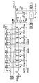
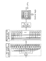
- FIG. A 32-phase clock oscillator, a narrow pulse generator, a pulse decimator, and a matrix switch are provided.
- the sampling holding unit samples and holds the input voltage at different timings, and each individual voltage-current conversion unit outputs a current corresponding thereto.
- the frequency characteristic of the conversion gain of the present voltage-current converter has an FIR filter characteristic by adding and outputting a part or all of the output current of the individual voltage-current converter.
- the sampling holding unit can be composed of only active elements by using the ground capacitance of the wiring and switching elements and the input capacitance of the individual voltage / current converting unit. Further, the individual voltage / current converter can also be composed of only active elements. Since the control unit can be composed of only logic circuits, the area is sufficiently small.
- the filter circuit using the present voltage-current converter does not necessarily require a capacity, and therefore has a small area even if it is high-ordered in order to obtain a steep cut-off characteristic. Further, since the bandwidth of this filter is proportional to the sampling frequency, it can be easily varied by controlling the sampling frequency. As described above, it is possible to obtain a variable filter having a small area and a sharp cutoff characteristic.
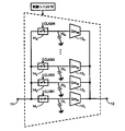
- FIG. 9 is a diagram showing the configuration of the voltage-current converter according to the second embodiment of the present invention.
- the voltage-current converter according to the present embodiment includes the individual voltage-current converters 1311, 1312, 1321, 1322, and the output terminal between each individual voltage-current converter and the terminal 17. It is characterized by having switching elements 1811, 1812, 1821, and 1822 connected in series. Further, the voltage-current conversion gains 1311 and 1321 are Gm0, and the voltage-current conversion gains 1312 and 1322 are -Gm0.
- the control unit 16 generates the two-phase clock signals CLKC1 and CLKC2 shown in FIG. 10 in addition to the CLKB1 and CLKB2 in FIG. 5, and controls the opening and closing of the opening / closing elements 1811, 1812, 1821 and 1822.
- CLKC1 and CLKC2 are clock signals that do not simultaneously become 1 but rise at the same timing as CLKB1 to CLKB2.
- the output terminal of the individual voltage-current converter (1311 or 1321) having the conversion gain Gm0 is compared with the input signal z-1Vin one sample before.
- the output terminal of the individual voltage-current converter (1312 or 1322) having a conversion gain of -Gm0 is controlled to be connected to the voltage-current converter output terminal 12.
- CLKC1 when CLKC1 is 1, the input voltage of the individual current converters 1311 and 1312 is Vin, and the input voltage of 1321 and 1322 is z ⁇ 1Vin.
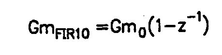
- the conversion gain GmFIR10 of the voltage-current converter according to the present embodiment is an expression including (1-z-1) representing the differentiation in the discrete time signal processing, as shown in Expression (2).
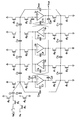
- FIG. 11 is a diagram showing the configuration of the voltage-current converter according to the third embodiment of the present invention.
- the voltage-current converter of the present embodiment includes individual voltage-current converters 1311 to 131N, 1321 to 132N,... 13N1 to 13NN, and the outputs of the individual voltage-current converters. It is characterized by having switching elements 1811 to 181N, 1821 to 182N,... 18N1 to 18NN connected in series between the terminal and the terminal 17.
- the conversion gains of 1311, 1321, ..., 13N1 are Gm1
- the conversion gains of 1312, 1322, ..., 13N2 are Gm2
- the conversion gains of 131N, 132N, ..., 13NN are GmN.
- the control unit 16 generates N-phase control clock signals CLKC1 to CLKCN shown in FIG. 12 in addition to CLKB1 to CLKBN of FIG. 5, and controls the opening and closing of the switching elements 1811 to 181N, 1821 to 182N,... 18N1 to 18NN.
- CLKC1 to CLKCN are clock signals that do not simultaneously become 1 but rise at the same timing as CLKB1 to CLKBN, respectively.
- As a method for obtaining CLKC1 to CLKCN there are a method of internally generating and a method of selecting from a plurality of clock signals supplied from the outside.
- the output of the individual voltage-current converter having the conversion gain Gmm + 1 with respect to the input signal z-mVin before m samples (m is an arbitrary integer from 0 to N).
- the terminal is controlled to be connected to the voltage / current converter output terminal 12.
- CLKC1 when CLKC1 is 1, the input voltages of the individual current converters 1311 to 1314, 1321 to 1324, 1331 to 1334, and 1341 to 1344 are Vin, z-1Vin, z-2Vin, and z-3Vin, respectively. It has become.
- the output terminals of 1311 whose conversion gain is Gm1, 1322 whose conversion gain is Gm2, 1333 whose conversion gain is Gm3, and 1344 whose conversion gain is Gm4 are connected to this voltage-current converter output terminal 12.
- the sum of the output current Gm1Vin of 1311, the output current z-1Gm2Vin of 1322, the output current z-2Gm3Vin of 1333, and the output current z-3Gm4Vin of 1344 is the output current of this voltage-current converter.
- the conversion gain GmFIR2 of the voltage-current converter of the present embodiment is a transfer function of a general FIR filter shown in Expression (3).
- the voltage-current converter according to the present embodiment can place a zero point in addition to a position that is an integral multiple of fCLK by selecting a coefficient.
- the signs of the conversion gains Gm1 to GmN of the individual voltage / current converters may be mixed.
- the individual voltage / current converters 1311 to 131N, 1321 to 132N,... 13N1 to 13NN do not necessarily have to be constantly operating. For example, the individual voltage / current converter 1311 only needs to operate while CLK1 is on. Further, it is not always necessary to arrange N ⁇ N individual voltage / current converters in parallel.
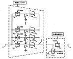
- FIG. 13 is a diagram showing the configuration of the voltage-current converter of the fourth embodiment of the present invention.
- the voltage-current converter of this embodiment is connected between the voltage-current converter (conversion gain GmFIR3) output terminal 17 of the first embodiment and the voltage-current converter output terminal 12 of this embodiment.
- the present invention is characterized in that an opening / closing element 191, an opening / closing element 192 connected between the terminal 17 and a fixed potential, and a gain control unit 20 for controlling opening / closing of the opening / closing element 191 and the opening / closing element 192 are added.
- the open / close element 191, the open / close element 192, and the gain control unit 20 are examples of a current extraction unit.
- the third embodiment may be used instead of the first embodiment.
- the gain control unit 20 generates the gain control clock signal CLKA and its inverted signal CLKA_INV shown in FIG. 14, and controls the opening / closing of the opening / closing element 191 and the opening / closing element 192, respectively.
- CLKA is a rectangular wave that repeats 0 and 1 at a constant period
- the open / close rate of the open / close element 191 is the on-time ratio of CLKA.
- the gain control unit 20 as a method for obtaining CLKA having a desired on-time ratio, there are a method of internally generating and a method of selecting from a plurality of clock signals supplied from the outside.
- the operation principle of the voltage-current converter of this embodiment will be described with reference to FIGS.
- the voltage Vin input to the input terminal 11 is converted into a current GmFIR3 ⁇ Vin flowing through the terminal 17 by the same operation as in the first embodiment.
- the switching element 19 1 When the switching element 19 1 is in the closed state, the current flowing through the terminal 17 is output as it is from the output terminal 12 and becomes the voltage-current converter output current of the present embodiment.
- the switching element 19 1 is opened, the terminal 17 and the output terminal 12 are disconnected, and the current flowing through the terminal 17 is passed through the switching element 192 to a fixed potential. At this time, the voltage-current converter output current of the present embodiment is zero.
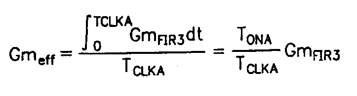
- the effective voltage-current conversion gain Gmeff when the converter output current of this embodiment is time-averaged is expressed by the following equation (4).
- Equation (3) means that the effective conversion gain Gmeff of the voltage-current converter of this embodiment is determined by the on-time ratio of CLKA (the ratio of TONA and TCLKA), that is, the switching ratio of the switching element 191. ing.
- the open / close ratio can be controlled with high accuracy by using a fine CMOS process, and can be varied over a wide range without causing performance degradation even under a low voltage.
- the open / close element 19 1, open / close element 19 2, and gain control unit 20 can be formed of a fine CMOS, there is almost no increase in area. Therefore, the conversion gain can be varied over a wide range without increasing the area even under a low voltage.
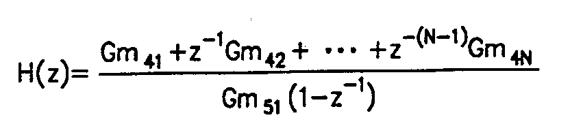
- FIG. 15 is a diagram showing a configuration of a filter circuit according to a fifth embodiment of the present invention. This embodiment is composed of the voltage-current converters 211 and 212 shown in FIG. 4, FIG. 9, FIG. 11, or FIG. The transfer function of this filter circuit is shown in equation (5).
- Equation (5) GmFIR4 and GmFIR5 are conversion gains of the voltage / current converters 211 and 212, respectively, and Gm41 to Gm4N and Gm51 to Gm5N are individual voltage / current converters constituting the voltage / current converters 211 and 212, respectively. Part conversion gain. Equation (5) is a transfer function of a general IIR filter, and the bandwidth of this filter is proportional to the sampling frequency, and therefore the bandwidth is variable in a very wide range.
- the filter order can be increased by increasing the number of juxtaposed individual voltage / current converters, and a filter circuit having a steep cutoff characteristic can be configured with a small area.
- the transfer function when GmFIR5 is configured by the voltage-current converter shown in FIG.
- Equation (6) shows that the transfer function of this filter circuit includes 1 / (1-z-1) representing the integration in the discrete-time signal processing. Considering that (1-z-1) can be approximated to j2 ⁇ fTsample when the sampling frequency 1 / Tsample is sufficiently large with respect to the signal frequency f, the voltage-current converter 212 effectively functions as a capacity of Gm51Tsample. . Therefore, the present invention can be easily applied by replacing the integrator using the capacitance with the present integrator in the filter designed by the related filter construction method.
- the voltage-current conversion gain with the opposite sign can be easily realized by inserting a current mirror circuit at the converter output terminal.
- it can be realized by switching the input / output connections of the positive phase and the negative phase.
- you may combine multiple types of the voltage-current converter of FIG.4, FIG.9, FIG.11 and FIG. 13 and the normal voltage-current converter with a flat frequency characteristic.
- the voltage-current converter of FIG. 4 or FIG. 11 is used on the input side
- the voltage-current converter of FIG. 13 is used on the output side
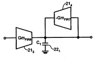
- FIG. 16 is a diagram showing a configuration of a filter circuit according to a sixth embodiment of the present invention.
- This embodiment includes the voltage-current converters 213 and 214 and the capacitor 221 shown in FIG. 4, FIG. 9, FIG. 11, or FIG.
- the transfer function of this filter circuit is shown in equation (7).
- GmFIR6 and GmFIR7 are conversion gains of the voltage / current converters 213 and 214, respectively, and Gm61 to Gm6N and Gm71 to Gm7N are individual voltage / current converters constituting the voltage / current converters 213 and 214, respectively. Part conversion gain. C1 indicates the capacitance value of the capacitor 22 1.
- the frequency characteristics of the FIR / IIR filter expressed only by the z function are symmetrical about the Nyquist frequency, which is half the sampling frequency, as shown in FIG. Then, the frequency characteristic below the sampling frequency is repeated. Therefore, a large number of passbands also exist in the frequency band above the sampling frequency.
- a capacitor element is added, and a filter configuration similar to that of a general Gm-C filter including a voltage-current converter and a capacitor is employed, so that the frequency characteristic of the continuous-time filter is superimposed on the transfer function. To do. As a result, an unnecessary pass band can be eliminated. This means that noise sampled in the pass band can be reduced during sampling in the voltage / current converter 214.
- the filter bandwidth is proportional not only to the sampling frequency but also to the conversion gain / capacitance ratio Gm / C. Therefore, when the bandwidth is variable, it is necessary to control the conversion gain or the capacitance value together with the sampling frequency. For example, when the sampling frequency is halved in order to halve the bandwidth, the conversion gain is also halved. At this time, if the converter of FIG. 13 is used, there is an advantage that the conversion gain can be easily made variable by changing the on-time ratio of CLKA in accordance with the sampling frequency, and the area does not increase.
- This filter circuit can also be applied to the configuration of a general second-order or higher Gm-C filter. Therefore, when forming a steeper filter, two methods can be used: a method of increasing the order of the FIR filter included in the voltage-current converter and a method of increasing the order of the Gm-C filter. Generally, in order to increase the order of the Gm-C filter, the number of capacitors increases, so the area greatly increases. However, by combining the above two methods, a high-order filter can be configured with a small area.
- the filter circuit of the present embodiment not all voltage-current converters necessarily have FIR filter characteristics.
- the converter 213 on the input side of the filter circuit of this embodiment uses a continuous-time processing converter having no FIR filter characteristics, and the voltage-current converter of FIG. If used, the noise in the vicinity of N ⁇ fCLK can be attenuated by the continuous-time processing filter formed by the voltage-current converter 213 and the capacitor 221, so that a filter inserted in the previous stage is not necessary.
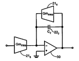
- FIG. 17 is a diagram showing the configuration of the filter circuit according to the seventh embodiment of the present invention.
- This embodiment includes the voltage / current converters 215 to 216, the capacitor 222, and the operational amplifier 30 shown in FIG.
- the transfer function of this filter circuit is shown in equation (9).
- GmFIR5 and GmFIR6 in the equation (9) indicate the conversion gains of the voltage-current converters 215 to 216, respectively, and C2 indicates the capacitance value of the capacitor 22.
- a filter having excellent linearity can be configured for the following two reasons. The first reason is that the output stage of each individual voltage / current converter does not need to handle a large signal. The second reason is that distortion caused by the gate-source voltage dependence of the on-resistance of the CMOS transmission gate used as the switching element does not occur particularly when the voltage-current converter of the fourth embodiment is used. That is. Note that the capacitor 22 2 is not necessarily used.
- FIG. 18 is a diagram showing the configuration of the eighth embodiment of the present invention.
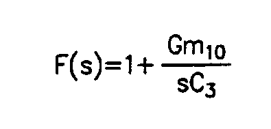
- a circuit in which a capacitor 24 is connected between an input terminal 25 and an output terminal 26 of a voltage-current converter 23 (conversion gain Gm10) as shown in FIG. May be used.
- Gm10 voltage-current converter 23
- a filter having an arbitrary transfer function such as a bandpass filter can be configured.
- Equation (11) means that FIR filtering can also be performed on a signal via the capacitor 24.
- FIG. 12 shows the case of the voltage-current converter of the first embodiment. Further, the conversion gains of the individual voltage / current converters 23 1 to 23 N and the capacitance values of the capacitors 24 1 to 24 N are not necessarily the same.
- the present invention is applicable to, for example, a voltage-current converter that converts an input voltage into a current and outputs the current.
- FIG. 1 is a circuit diagram showing a first embodiment of the present invention. It is a figure which shows the timing of the clock signal of the 1st Embodiment of this invention. It is a figure which shows the frequency characteristic of the 1st Embodiment of this invention. 1 is a circuit diagram showing a first embodiment of the present invention. It is a figure which shows the control unit of the 1st Embodiment of this invention. It is a circuit diagram which shows the 2nd Embodiment of this invention. It is a figure which shows the timing of the clock signal of the 2nd Embodiment of this invention.
Landscapes
- Networks Using Active Elements (AREA)
- Analogue/Digital Conversion (AREA)
- Amplifiers (AREA)
Abstract
Description
図4は本発明の第1の実施の形態の電圧電流変換器の構成を示す図である。

図9は本発明の第2の実施の形態の電圧電流変換器の構成を示す図である。本実施の形態の電圧電流変換器は、第1の実施形態と比較して、個別電圧電流変換部1311、1312、1321、1322と、各々の個別電圧電流変換部の出力端子と端子17の間に直列に接続された開閉素子1811、1812、1821、1822を有する点を特徴とする。さらに、1311、1321の電圧電流変換利得はGm0であり、1312、1322の電圧電流変換利得は-Gm0である。


特に、GmFIR5を、図9に示した電圧電流変換器で構成した場合の伝達関数を式(6)に示す。
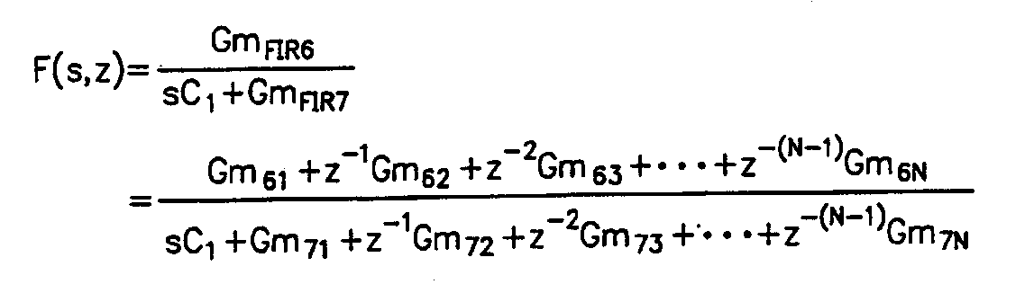
特に、GmFIR7を、図9に示した電圧電流変換器で構成した場合の伝達関数を式(8)に示す。



Claims (11)
- 入力された電圧を電流に変換して出力する電圧電流変換器であって、
入力された電圧を標本化して保持する機能を持つ1つ以上の標本化保持部と、
前記標本化保持部によって標本化して保持されている電圧に対応する電流を出力する1つ以上の個別電圧電流変換部と、
前記標本化保持部が入力電圧を標本化して保持するタイミングを制御する制御部と
を有し、
前記個別電圧電流変換部の出力電流の一部または全てを加算して出力することによって、本電圧電流変換器の変換利得の周波数特性が有限インパルス応答または無限インパルス応答フィルタ特性となることを特徴とする電圧電流変換器。 - 前記標本化保持部は、開閉素子と容量を含み、前記容量は、配線または前記開閉素子の対地容量、または後段の個別電圧電流変換部の入力容量であることを特徴とする請求項1記載の電圧電流変換器。
- 前記標本化保持部は、各々が等しい時間間隔で入力電圧を標本化して保持し、
前記個別電圧電流変換部の変換利得は、全て等しい変換利得を有し、前記個別電圧電流変換部の出力電流の一部または全てを加算して出力することによって、本電圧電流変換器の変換利得の周波数特性が、移動平均フィルタ特性を有することを特徴とする請求項1記載の電圧電流変換器。 - 前記電圧電流変換器は、前記個別電圧電流変換部出力端子から流れる電流を間欠的に取り出して出力するための電流取出部をさらに有し、実効的な電圧電流変換利得が、電流取出部の間欠動作比率によって制御されることを特徴とする請求項1記載の電圧電流変換器。
- 請求項1から4のいずれか1項に記載の電圧電流変換器を1つ以上用いて構成したことを特徴とする微分回路。
- 前記電圧電流変換器出力端子には、容量素子が接続されることを特徴とする請求項5記載の微分回路。
- 請求項1から4のいずれか1項に記載の電圧電流変換器を1つ以上用いて構成したことを特徴とする積分回路。
- 前記電圧電流変換器出力端子には、容量素子が接続されることを特徴とする請求項7記載の積分回路。
- 請求項1から4のいずれか1項に記載の電圧電流変換器を1つ以上用いて構成したことを特徴とするフィルタ回路。
- 請求項9記載のフィルタ回路において、前記電圧電流変換器出力端子には、容量素子が接続されることを特徴とするフィルタ回路。
- 入力された電圧を標本化して保持し、
標本化して保持された電圧に対応する電流を出力する際に出力電流の一部または全てを加算して出力して、変換利得の周波数特性を有限インパルス応答または無限インパルス応答フィルタ特性とすることを特徴とする電圧電流変換方法。
Priority Applications (3)
| Application Number | Priority Date | Filing Date | Title |
|---|---|---|---|
| JP2009551517A JP5515743B2 (ja) | 2008-01-28 | 2009-01-27 | 電圧電流変換器、それを用いた、微分回路、積分回路およびフィルタ回路並びに電圧電流変換方法 |
| US12/863,741 US8248111B2 (en) | 2008-01-28 | 2009-01-27 | Voltage current converter, differentiation circuit, integration circuit, and filter circuit using the converter, and voltage current conversion method |
| CN200980103384.7A CN101926091B (zh) | 2008-01-28 | 2009-01-27 | 电压电流转换器、微分电路、积分电路、使用该转换器的滤波器电路、及电压电流转换方法 |
Applications Claiming Priority (4)
| Application Number | Priority Date | Filing Date | Title |
|---|---|---|---|
| JP2008-016264 | 2008-01-28 | ||
| JP2008016264 | 2008-01-28 | ||
| JP2008-177997 | 2008-07-08 | ||
| JP2008177997 | 2008-07-08 |
Publications (1)
| Publication Number | Publication Date |
|---|---|
| WO2009096376A1 true WO2009096376A1 (ja) | 2009-08-06 |
Family
ID=40912729
Family Applications (1)
| Application Number | Title | Priority Date | Filing Date |
|---|---|---|---|
| PCT/JP2009/051243 Ceased WO2009096376A1 (ja) | 2008-01-28 | 2009-01-27 | 電圧電流変換器、それを用いた、微分回路、積分回路およびフィルタ回路並びに電圧電流変換方法 |
Country Status (4)
| Country | Link |
|---|---|
| US (1) | US8248111B2 (ja) |
| JP (1) | JP5515743B2 (ja) |
| CN (1) | CN101926091B (ja) |
| WO (1) | WO2009096376A1 (ja) |
Families Citing this family (4)
| Publication number | Priority date | Publication date | Assignee | Title |
|---|---|---|---|---|
| WO2013190701A1 (ja) * | 2012-06-22 | 2013-12-27 | 下西技研工業株式会社 | 重送検知装置及びシート状物取り扱い装置 |
| CN106788276B (zh) * | 2015-12-29 | 2020-03-13 | 深圳市汇顶科技股份有限公司 | 转换电路及检测电路 |
| CN106888029B (zh) * | 2017-01-18 | 2019-05-24 | 锐迪科微电子(上海)有限公司 | 一种省略片外滤波器的接收机 |
| EP3982535B1 (en) * | 2019-06-29 | 2026-02-25 | Huawei Technologies Co., Ltd. | Rc oscillator |
Citations (4)
| Publication number | Priority date | Publication date | Assignee | Title |
|---|---|---|---|---|
| JP2002541709A (ja) * | 1999-04-05 | 2002-12-03 | ソニック イノヴェイションズ インコーポレイテッド | ハイブリッド低域シグマ−デルタ変調器 |
| JP2003158444A (ja) * | 2002-11-06 | 2003-05-30 | Yamaha Corp | アナログ信号の遅延回路 |
| JP2003317026A (ja) * | 2002-04-19 | 2003-11-07 | Univ Waseda | 符号付積和演算器およびこれを含むアナログマッチドフィルタ |
| JP2007324659A (ja) * | 2006-05-30 | 2007-12-13 | Sony Corp | チャージドメインフィルタ回路 |
Family Cites Families (3)
| Publication number | Priority date | Publication date | Assignee | Title |
|---|---|---|---|---|
| JP2002176358A (ja) | 2000-12-05 | 2002-06-21 | Toshiba Lsi System Support Kk | A/dコンバータ |
| CN100426670C (zh) * | 2002-08-15 | 2008-10-15 | 联发科技股份有限公司 | 多相滤波器电路 |
| US7479812B1 (en) * | 2005-05-27 | 2009-01-20 | National Semiconductor Corporation | Producing a frequency-representative signal with rapid adjustment to frequency changes |
-
2009
- 2009-01-27 WO PCT/JP2009/051243 patent/WO2009096376A1/ja not_active Ceased
- 2009-01-27 US US12/863,741 patent/US8248111B2/en active Active
- 2009-01-27 JP JP2009551517A patent/JP5515743B2/ja active Active
- 2009-01-27 CN CN200980103384.7A patent/CN101926091B/zh not_active Expired - Fee Related
Patent Citations (4)
| Publication number | Priority date | Publication date | Assignee | Title |
|---|---|---|---|---|
| JP2002541709A (ja) * | 1999-04-05 | 2002-12-03 | ソニック イノヴェイションズ インコーポレイテッド | ハイブリッド低域シグマ−デルタ変調器 |
| JP2003317026A (ja) * | 2002-04-19 | 2003-11-07 | Univ Waseda | 符号付積和演算器およびこれを含むアナログマッチドフィルタ |
| JP2003158444A (ja) * | 2002-11-06 | 2003-05-30 | Yamaha Corp | アナログ信号の遅延回路 |
| JP2007324659A (ja) * | 2006-05-30 | 2007-12-13 | Sony Corp | チャージドメインフィルタ回路 |
Non-Patent Citations (1)
| Title |
|---|
| "Solid-State Circuits Conference, 2008. ISSCC 2008. Digest of Technical Papers., 2008.02.03", article MASAKI KITSUNEZUKA ET AL.: "A Widely-Tunable Reconfigurable CMOS Analog Baseband IC for Software-Defined Radio", pages: 66 - 67, 595 * |
Also Published As
| Publication number | Publication date |
|---|---|
| CN101926091A (zh) | 2010-12-22 |
| US20100289533A1 (en) | 2010-11-18 |
| US8248111B2 (en) | 2012-08-21 |
| JP5515743B2 (ja) | 2014-06-11 |
| JPWO2009096376A1 (ja) | 2011-05-26 |
| CN101926091B (zh) | 2014-07-16 |
Similar Documents
| Publication | Publication Date | Title |
|---|---|---|
| JP5240193B2 (ja) | 電圧電流変換器およびこれを用いたフィルタ回路 | |
| US7535288B2 (en) | Charge domain filter device | |
| US8385874B2 (en) | Discrete time direct sampling circuit and receiver | |
| CN102916677B (zh) | 无限脉冲响应滤波器以及滤波方法 | |
| CN102106084A (zh) | 离散时间多速率模拟滤波器 | |
| CN101395798A (zh) | 离散时间直接采样电路及接收器 | |
| Kitsunezuka et al. | A widely-tunable, reconfigurable CMOS analog baseband IC for software-defined radio | |
| US20110170640A1 (en) | Sampling circuit and receiver | |
| US9647679B1 (en) | Methods and apparatus for a delta sigma ADC with parallel-connected integrators | |
| JP5515743B2 (ja) | 電圧電流変換器、それを用いた、微分回路、積分回路およびフィルタ回路並びに電圧電流変換方法 | |
| CN102017410B (zh) | 开关电容器抽选器 | |
| JP5046622B2 (ja) | サンプリングフィルタ装置 | |
| EP2081294B1 (en) | Programmable filter circuits and methods | |
| WO2008050630A1 (en) | Sampling filter device and radio communication device | |
| US20100105349A1 (en) | Rf signal sampling apparatus and method | |
| JP5038069B2 (ja) | フィルタ回路及びこれを用いた通信用半導体装置 | |
| US20070008208A1 (en) | Filter with gain | |
| US7941475B2 (en) | Programmable filter circuits and methods | |
| JP5393607B2 (ja) | ダイレクトサンプリング回路 | |
| JP2008219413A (ja) | 可変フィルタ | |
| US8369817B2 (en) | Analog FIR filter | |
| Choi et al. | A programmable discrete-time filter employing hardware-efficient two-dimensional implementation method |
Legal Events
| Date | Code | Title | Description |
|---|---|---|---|
| WWE | Wipo information: entry into national phase |
Ref document number: 200980103384.7 Country of ref document: CN |
|
| 121 | Ep: the epo has been informed by wipo that ep was designated in this application |
Ref document number: 09706605 Country of ref document: EP Kind code of ref document: A1 |
|
| WWE | Wipo information: entry into national phase |
Ref document number: 12863741 Country of ref document: US |
|
| WWE | Wipo information: entry into national phase |
Ref document number: 2009551517 Country of ref document: JP |
|
| NENP | Non-entry into the national phase |
Ref country code: DE |
|
| 122 | Ep: pct application non-entry in european phase |
Ref document number: 09706605 Country of ref document: EP Kind code of ref document: A1 |