WO2009104239A1 - Dispositif de mémoire non volatile et son procédé de fabrication - Google Patents
Dispositif de mémoire non volatile et son procédé de fabrication Download PDFInfo
- Publication number
- WO2009104239A1 WO2009104239A1 PCT/JP2008/052636 JP2008052636W WO2009104239A1 WO 2009104239 A1 WO2009104239 A1 WO 2009104239A1 JP 2008052636 W JP2008052636 W JP 2008052636W WO 2009104239 A1 WO2009104239 A1 WO 2009104239A1
- Authority
- WO
- WIPO (PCT)
- Prior art keywords
- layer
- memory device
- nonvolatile memory
- phase change
- wiring
- Prior art date
- Legal status (The legal status is an assumption and is not a legal conclusion. Google has not performed a legal analysis and makes no representation as to the accuracy of the status listed.)
- Ceased
Links
Images


Classifications
-
- H—ELECTRICITY
- H10—SEMICONDUCTOR DEVICES; ELECTRIC SOLID-STATE DEVICES NOT OTHERWISE PROVIDED FOR
- H10N—ELECTRIC SOLID-STATE DEVICES NOT OTHERWISE PROVIDED FOR
- H10N70/00—Solid-state devices having no potential barriers, and specially adapted for rectifying, amplifying, oscillating or switching
- H10N70/20—Multistable switching devices, e.g. memristors
- H10N70/231—Multistable switching devices, e.g. memristors based on solid-state phase change, e.g. between amorphous and crystalline phases, Ovshinsky effect
-
- H—ELECTRICITY
- H10—SEMICONDUCTOR DEVICES; ELECTRIC SOLID-STATE DEVICES NOT OTHERWISE PROVIDED FOR
- H10B—ELECTRONIC MEMORY DEVICES
- H10B63/00—Resistance change memory devices, e.g. resistive RAM [ReRAM] devices
- H10B63/20—Resistance change memory devices, e.g. resistive RAM [ReRAM] devices comprising selection components having two electrodes, e.g. diodes
-
- H—ELECTRICITY
- H10—SEMICONDUCTOR DEVICES; ELECTRIC SOLID-STATE DEVICES NOT OTHERWISE PROVIDED FOR
- H10B—ELECTRONIC MEMORY DEVICES
- H10B63/00—Resistance change memory devices, e.g. resistive RAM [ReRAM] devices
- H10B63/80—Arrangements comprising multiple bistable or multi-stable switching components of the same type on a plane parallel to the substrate, e.g. cross-point arrays
- H10B63/84—Arrangements comprising multiple bistable or multi-stable switching components of the same type on a plane parallel to the substrate, e.g. cross-point arrays arranged in a direction perpendicular to the substrate, e.g. 3D cell arrays
-
- H—ELECTRICITY
- H10—SEMICONDUCTOR DEVICES; ELECTRIC SOLID-STATE DEVICES NOT OTHERWISE PROVIDED FOR
- H10N—ELECTRIC SOLID-STATE DEVICES NOT OTHERWISE PROVIDED FOR
- H10N70/00—Solid-state devices having no potential barriers, and specially adapted for rectifying, amplifying, oscillating or switching
- H10N70/011—Manufacture or treatment of multistable switching devices
- H10N70/021—Formation of switching materials, e.g. deposition of layers
- H10N70/026—Formation of switching materials, e.g. deposition of layers by physical vapor deposition, e.g. sputtering
-
- H—ELECTRICITY
- H10—SEMICONDUCTOR DEVICES; ELECTRIC SOLID-STATE DEVICES NOT OTHERWISE PROVIDED FOR
- H10N—ELECTRIC SOLID-STATE DEVICES NOT OTHERWISE PROVIDED FOR
- H10N70/00—Solid-state devices having no potential barriers, and specially adapted for rectifying, amplifying, oscillating or switching
- H10N70/011—Manufacture or treatment of multistable switching devices
- H10N70/041—Modification of switching materials after formation, e.g. doping
- H10N70/043—Modification of switching materials after formation, e.g. doping by implantation
-
- H—ELECTRICITY
- H10—SEMICONDUCTOR DEVICES; ELECTRIC SOLID-STATE DEVICES NOT OTHERWISE PROVIDED FOR
- H10N—ELECTRIC SOLID-STATE DEVICES NOT OTHERWISE PROVIDED FOR
- H10N70/00—Solid-state devices having no potential barriers, and specially adapted for rectifying, amplifying, oscillating or switching
- H10N70/011—Manufacture or treatment of multistable switching devices
- H10N70/041—Modification of switching materials after formation, e.g. doping
- H10N70/046—Modification of switching materials after formation, e.g. doping by diffusion, e.g. photo-dissolution
-
- H—ELECTRICITY
- H10—SEMICONDUCTOR DEVICES; ELECTRIC SOLID-STATE DEVICES NOT OTHERWISE PROVIDED FOR
- H10N—ELECTRIC SOLID-STATE DEVICES NOT OTHERWISE PROVIDED FOR
- H10N70/00—Solid-state devices having no potential barriers, and specially adapted for rectifying, amplifying, oscillating or switching
- H10N70/011—Manufacture or treatment of multistable switching devices
- H10N70/061—Shaping switching materials
- H10N70/063—Shaping switching materials by etching of pre-deposited switching material layers, e.g. lithography
-
- H—ELECTRICITY
- H10—SEMICONDUCTOR DEVICES; ELECTRIC SOLID-STATE DEVICES NOT OTHERWISE PROVIDED FOR
- H10N—ELECTRIC SOLID-STATE DEVICES NOT OTHERWISE PROVIDED FOR
- H10N70/00—Solid-state devices having no potential barriers, and specially adapted for rectifying, amplifying, oscillating or switching
- H10N70/801—Constructional details of multistable switching devices
- H10N70/821—Device geometry
- H10N70/826—Device geometry adapted for essentially vertical current flow, e.g. sandwich or pillar type devices
-
- H—ELECTRICITY
- H10—SEMICONDUCTOR DEVICES; ELECTRIC SOLID-STATE DEVICES NOT OTHERWISE PROVIDED FOR
- H10N—ELECTRIC SOLID-STATE DEVICES NOT OTHERWISE PROVIDED FOR
- H10N70/00—Solid-state devices having no potential barriers, and specially adapted for rectifying, amplifying, oscillating or switching
- H10N70/801—Constructional details of multistable switching devices
- H10N70/841—Electrodes
-
- H—ELECTRICITY
- H10—SEMICONDUCTOR DEVICES; ELECTRIC SOLID-STATE DEVICES NOT OTHERWISE PROVIDED FOR
- H10N—ELECTRIC SOLID-STATE DEVICES NOT OTHERWISE PROVIDED FOR
- H10N70/00—Solid-state devices having no potential barriers, and specially adapted for rectifying, amplifying, oscillating or switching
- H10N70/801—Constructional details of multistable switching devices
- H10N70/881—Switching materials
- H10N70/882—Compounds of sulfur, selenium or tellurium, e.g. chalcogenides
- H10N70/8828—Tellurides, e.g. GeSbTe
-
- G—PHYSICS
- G11—INFORMATION STORAGE
- G11C—STATIC STORES
- G11C13/00—Digital stores characterised by the use of storage elements not covered by groups G11C11/00, G11C23/00, or G11C25/00
- G11C13/0002—Digital stores characterised by the use of storage elements not covered by groups G11C11/00, G11C23/00, or G11C25/00 using resistive RAM [RRAM] elements
- G11C13/0004—Digital stores characterised by the use of storage elements not covered by groups G11C11/00, G11C23/00, or G11C25/00 using resistive RAM [RRAM] elements comprising amorphous/crystalline phase transition cells
-
- G—PHYSICS
- G11—INFORMATION STORAGE
- G11C—STATIC STORES
- G11C2213/00—Indexing scheme relating to G11C13/00 for features not covered by this group
- G11C2213/70—Resistive array aspects
- G11C2213/72—Array wherein the access device being a diode
-
- Y—GENERAL TAGGING OF NEW TECHNOLOGICAL DEVELOPMENTS; GENERAL TAGGING OF CROSS-SECTIONAL TECHNOLOGIES SPANNING OVER SEVERAL SECTIONS OF THE IPC; TECHNICAL SUBJECTS COVERED BY FORMER USPC CROSS-REFERENCE ART COLLECTIONS [XRACs] AND DIGESTS
- Y10—TECHNICAL SUBJECTS COVERED BY FORMER USPC
- Y10S—TECHNICAL SUBJECTS COVERED BY FORMER USPC CROSS-REFERENCE ART COLLECTIONS [XRACs] AND DIGESTS
- Y10S257/00—Active solid-state devices, e.g. transistors, solid-state diodes
- Y10S257/92—Conductor layers on different levels connected in parallel, e.g. to reduce resistance
-
- Y—GENERAL TAGGING OF NEW TECHNOLOGICAL DEVELOPMENTS; GENERAL TAGGING OF CROSS-SECTIONAL TECHNOLOGIES SPANNING OVER SEVERAL SECTIONS OF THE IPC; TECHNICAL SUBJECTS COVERED BY FORMER USPC CROSS-REFERENCE ART COLLECTIONS [XRACs] AND DIGESTS
- Y10—TECHNICAL SUBJECTS COVERED BY FORMER USPC
- Y10S—TECHNICAL SUBJECTS COVERED BY FORMER USPC CROSS-REFERENCE ART COLLECTIONS [XRACs] AND DIGESTS
- Y10S977/00—Nanotechnology
- Y10S977/70—Nanostructure
- Y10S977/701—Integrated with dissimilar structures on a common substrate
- Y10S977/712—Integrated with dissimilar structures on a common substrate formed from plural layers of nanosized material, e.g. stacked structures
-
- Y—GENERAL TAGGING OF NEW TECHNOLOGICAL DEVELOPMENTS; GENERAL TAGGING OF CROSS-SECTIONAL TECHNOLOGIES SPANNING OVER SEVERAL SECTIONS OF THE IPC; TECHNICAL SUBJECTS COVERED BY FORMER USPC CROSS-REFERENCE ART COLLECTIONS [XRACs] AND DIGESTS
- Y10—TECHNICAL SUBJECTS COVERED BY FORMER USPC
- Y10S—TECHNICAL SUBJECTS COVERED BY FORMER USPC CROSS-REFERENCE ART COLLECTIONS [XRACs] AND DIGESTS
- Y10S977/00—Nanotechnology
- Y10S977/70—Nanostructure
- Y10S977/734—Fullerenes, i.e. graphene-based structures, such as nanohorns, nanococoons, nanoscrolls or fullerene-like structures, e.g. WS2 or MoS2 chalcogenide nanotubes, planar C3N4, etc.
Definitions
- the present invention relates to a nonvolatile memory device and a method for manufacturing the same, and more particularly, to a nonvolatile memory including a phase change film including a material that changes between a crystalline state and an amorphous state by applying a voltage.
- the present invention relates to an apparatus and a manufacturing method thereof.
- NAND flash memory and small HDD have rapidly evolved in recording density and formed a large market.
- both the NAND flash memory and the small HDD are expected to face the limit of recording density in the future.
- the NAND flash memory uses a transistor for the storage portion, miniaturization is expected to reach the limit due to the so-called short channel effect.
- the “short channel effect” is a phenomenon that occurs when the distance between the source portion and the drain portion is reduced due to miniaturization of the device, and specific examples include an increase in leakage current between the source and the drain.
- the manufacturing cost is increased due to the reduction of the minimum line width.
- the tracking accuracy accuracy of aligning the head with the correct position of the track on the HDD is expected to reach its limit.
- phase change nonvolatile memory device uses a characteristic that a phase change film changes between a crystalline state and an amorphous state by applying an electric field pulse to a semiconductor film (phase change film) It is. By reversibly converting the high resistance state (amorphous state, on) and the low resistance state (crystalline state, off) in the phase change film, information can be rewritten and the power can be turned off. Information is stored so that it will not disappear. Since the high-resistance and low-resistance states of the phase change film are stable, non-volatility is realized.
- the phase change type nonvolatile memory device does not have a problem that may occur in the above-described NAND flash memory or small HDD, and is considered superior to the former two in terms of high speed and miniaturization.
- phase change type nonvolatile memory device since a relatively large current flows at the time of operation, particularly at the time of erasing (reset), reduction of this operating current is required.
- nitrogen, oxygen or carbon ions are doped in a semiconductor integrated circuit device using an alloy film (GST film) of germanium (Ge), antimony (Sb) and tellurium (Te) as a memory element.
- GST film germanium
- Sb antimony
- Te tellurium
- a specific example is that a region where oxygen ions of high concentration are implanted has almost insulating properties, and a current for rewriting and signal transmission is limited to a region where ions are implanted at a low concentration (patent) Reference 1).
- the present invention relates to a nonvolatile memory device including a phase change film including a material that changes between a crystalline state and an amorphous state by applying a voltage, and can reduce power consumption. And a method for manufacturing the same.
- the first layer, the second layer, and the first layer and the second layer are sandwiched between the first layer and the second layer.
- a recording layer capable of reversibly transitioning between a first state having a low resistance and a second state having a high resistance by a current supplied through the layer, wherein the recording layer includes a main layer In the plane of the surface, there is provided a non-volatile memory device having a first portion and a second portion having a relatively higher nitrogen content than the first portion.
- the resistance is caused by a current sandwiched between the first layer and the second layer and supplied through the first layer and the second layer.
- a method for manufacturing a nonvolatile memory device having a recording layer capable of reversibly transitioning between a low first state and a high resistance second state, the first layer and a recording layer containing nitrogen And a second layer, and a step of removing nitrogen from the side surface of the recording layer.
- a method for manufacturing a nonvolatile memory device is provided. .
- a resistance is obtained by a current sandwiched between the first layer and the second layer and supplied through the first layer and the second layer.
- a method for manufacturing a nonvolatile memory device having a recording layer capable of reversibly transitioning between a first state having a low resistance and a second state having a high resistance, wherein the first layer, the recording layer There is provided a method for manufacturing a nonvolatile memory device, comprising: a step of forming a stacked body including two layers; and a step of introducing nitrogen from a side surface of the recording layer.
- a resistance is obtained by a current sandwiched between the first layer and the second layer and supplied through the first layer and the second layer.
- a method for manufacturing a nonvolatile memory device is provided. That.
- FIG. 1 is a schematic cross-sectional view illustrating an example (specific example 1) of a nonvolatile memory device according to a first embodiment of the present invention. It is a schematic cross section showing another example (specific example 2) of the nonvolatile memory device according to the first embodiment of the present invention. It is a conceptual diagram for demonstrating the operation mechanism of the non-volatile memory device which concerns on this embodiment.
- (A) is a schematic cross-sectional view of the phase change film 40 for representing the effect of the specific example 1
- (b) is a schematic cross-sectional view of the phase change film 40 for representing the effect of the specific example 2.
- FIG. 6 is a schematic cross-sectional view of a phase change film 40 for explaining an effect of a specific example 2.
- FIG. 12 is a process cross-sectional view illustrating an example of a method for manufacturing the nonvolatile memory device in specific example 1.
- FIG. 12 is a process cross-sectional view illustrating another example of the manufacturing method according to the nonvolatile memory device in specific example 1.
- FIG. 12 is a process cross-sectional view illustrating another example of the manufacturing method according to the nonvolatile memory device in specific example 1.
- FIG. 12 is a process cross-sectional view illustrating an example of a manufacturing method according to the nonvolatile memory device in specific example 2.
- FIG. 12 is a process cross-sectional view illustrating another example of the method for manufacturing the nonvolatile memory device in specific example 2.
- FIG. 12 is a process cross-sectional view illustrating another example of the method for manufacturing the nonvolatile memory device in specific example 2.
- FIG. It is a schematic diagram showing an example (specific example 3) of the nonvolatile memory device according to the third embodiment of the present invention.
- 12 is a process cross-sectional view illustrating an example of a method for manufacturing the nonvolatile memory device in specific example 3.
- FIG. 12 is a process cross-sectional view illustrating another example of the manufacturing method according to the nonvolatile memory device in specific example 3.
- FIG. 12 is a process cross-sectional view illustrating another example of the manufacturing method according to the nonvolatile memory device in specific example 3.
- FIG. FIG. 9 is a schematic view illustrating a nonvolatile memory device according to a fifth embodiment of the invention.
- FIG. 17 is a schematic diagram illustrating a circuit of the nonvolatile memory device illustrated in FIG. 16.
- nonvolatile memory device 2 nonvolatile memory device 2a first layer nonvolatile memory device 2b second layer nonvolatile memory device 4 nonvolatile memory device 6 nonvolatile memory device 10 first wiring 20 rectifying element 30 first electrode 40 phase change film 42 Low nitrogen concentration portion 44 High nitrogen concentration portion 46 Nitrogen oxygen introduction portion 48 Phase change material film 50 Second electrode 60 Second wiring 70 Dummy mask 105 Substrate 106 Main surface 110 First wiring 110a First first layer Wiring 110b second-layer first wiring 115 word line driver and decoder 120 second wiring 120a first-layer second wiring 120b second-layer second wiring 125 bit-line driver, decoder, and readout circuit 140 Rectifying element unit 140a Switch element unit 140b Switch element unit 200 Storage unit 200a First layer storage unit 200b Second layer storage unit
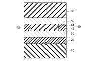
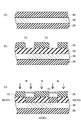
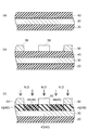
- FIG. 1 is a schematic cross-sectional view showing an example (specific example 1) of the nonvolatile memory device according to the first embodiment of the invention.
- the nonvolatile memory device of this specific example includes a first wiring 10, a rectifying element 20 provided on the first wiring 10, and a first electrode (first electrode provided on the rectifying element 20. Layer) 30, a phase change film (recording layer) 40 provided on the main surface of the first electrode 30, and a second electrode (second layer) provided on the main surface of the phase change film 40.
- the “main surface” means a surface perpendicular to the stacking direction (vertical direction in FIG. 1) of the first electrode 30, the phase change film 40, the second electrode 50, and the like.
- the phase change film 40 contains nitrogen in whole or in part, and a second portion (high nitrogen concentration portion 44) having a relatively high nitrogen concentration is formed inside the main surface, and the main surface.
- the first portion (low nitrogen concentration portion 42) having a relatively low nitrogen concentration is provided on the outside in the plane. That is, the low nitrogen concentration portion 42 is provided so as to surround the high nitrogen concentration portion 44 in the main surface.
- a heater layer made of a material having a resistivity of, for example, about 10 ⁇ 5 ⁇ cm or more is provided on the first electrode 30 side or the second electrode 50 side. (Not shown) may be provided.
- the rectifying element 20 is made of a diode, for example.
- the first electrode 30 and the second electrode 50 can be made of a material that is not easily oxidized in consideration of the case where the entire element is oxidized. Examples of such materials include the compounds listed below.
- MN M is at least one element selected from the group consisting of Ti, Zr, Hf, V, Nb, and Ta. N is nitrogen.
- MO x M is from the group of Ti, V, Cr, Mn, Fe, Co, Ni, Cu, Zr, Nb, Mo, Ru, Rh, Pd, Ag, Hf, Ta, W, Re, Ir, Os, and Pt. At least one element selected. x satisfies 1 ⁇ x ⁇ 4. O is oxygen.
- (C) AMO 3 A is at least one element selected from the group of La, K, Ca, Sr, Ba, and Ln (lanthanoid).
- M is from the group of Ti, V, Cr, Mn, Fe, Co, Ni, Cu, Zr, Nb, Mo, Ru, Rh, Pd, Ag, Hf, Ta, W, Re, Ir, Os, and Pt.
- At least one element selected. O is oxygen.
- a 2 MO 4 A is at least one element selected from the group of K, Ca, Sr, Ba, and Ln (lanthanoid).
- M is from the group of Ti, V, Cr, Mn, Fe, Co, Ni, Cu, Zr, Nb, Mo, Ru, Rh, Pd, Ag, Hf, Ta, W, Re, Ir, Os, and Pt.
- At least one element selected. O is oxygen.
- the phase change film 40 includes a material that changes between a crystalline state and an amorphous state by applying a voltage.
- this material include chalcogenide-based materials.
- Chalcogenide is a general term for compounds containing group 16 elements such as Se and Te, and is derived from the fact that group 16 elements are called chalcogens.
- Specific examples include those containing Se or Te, and more specifically, Ge 2 Sb 2 Te 5 , GeSbTe, SbTe, AsSbTe, SeSbTe, AgInSbTe, and the like.
- crystal does not mean a complete crystal but includes a single crystal and a polycrystal state including defects.
- amorphous does not mean only those having a completely disordered atomic arrangement, but those having a short-range periodic structure or containing fine crystal grains in a disordered matrix. Also included in “amorphous”.
- the phase change film 40 is produced by introducing nitrogen into all or part of the above materials.
- the purpose of introducing nitrogen is to stabilize the crystalline or amorphous state. When nitrogen is introduced, the phase change temperature rises, so that the phase change is less likely to occur. As a result, the recorded information is not easily erased, and non-volatility is ensured.
- the high nitrogen concentration portion 44 is a portion having a relatively high nitrogen concentration
- the low nitrogen concentration portion 42 is a portion having a relatively low nitrogen concentration.
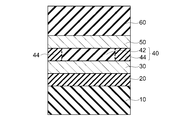
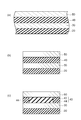
- FIG. 2 is a schematic cross-sectional view showing another example (specific example 2) of the nonvolatile memory device according to the first embodiment of the invention.
- the nonvolatile memory device of this example includes a first wiring 10, a rectifying element 20 provided on the first wiring 10, a first electrode 30 provided on the rectifying element 20, Phase change film 40 provided on the main surface of one electrode 30, second electrode 50 provided on the main surface of phase change film 40, and provided on second electrode 50 A second wiring 60.
- the phase change film 40 contains nitrogen in whole or in part, and the first portion (low nitrogen concentration portion 42) having a relatively low nitrogen concentration is formed inside the main surface, and the main surface.
- the second portion (high nitrogen concentration portion 44) having a relatively high nitrogen concentration is provided on the outside in the plane. That is, the high nitrogen concentration portion 44 is provided so as to surround the low nitrogen concentration portion 42 in the main surface.
- a material having a resistivity of, for example, about 10 ⁇ 5 ⁇ cm or more is provided on the first electrode 30 side or the second electrode 50 side.
- a heater layer (not shown) may be provided.
- Constituent materials and the like of the rectifying element 20, the first electrode 30, the second electrode 50, and the phase change film 40 of this specific example can be the same as those described above regarding the specific example 1.
- Example 1 The difference from Example 1 is that the positional relationship between the high nitrogen concentration portion 44 and the low nitrogen concentration portion 42 is reversed. That is, in the specific example 1, the low nitrogen concentration portion 42 is disposed outside in the plane of the main surface, whereas in the specific example 2, the low nitrogen concentration portion 42 is disposed inside in the plane of the main surface.
- phase change film 40 has portions with different nitrogen concentrations in the main surface. Specific examples 1 and 2 both have this feature.
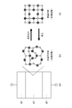
- FIG. 3 is a conceptual diagram for explaining an operation mechanism of the nonvolatile memory device according to the present embodiment.
- 3A is a schematic cross-sectional view showing the vicinity of the phase change film 40 of the nonvolatile memory device according to this embodiment.
- FIG. 3B is a schematic diagram showing a structure of an amorphous state of chalcogenide that can be a material of the phase change film 40, specifically, Ge 2 Sb 2 Te 5 .
- this compound has a structure composed of various rings such as a 4-membered ring, a 6-membered ring, and an 8-membered ring.
- FIG. 3 (c) is a schematic view illustrating the structure of the crystalline state of Ge 2 Sb 2 Te 5.
- this compound has a structure consisting of only a 4-membered ring, a 6-membered ring, and an 8-membered ring.
- a chalcogenide such as Ge 2 Sb 2 Te 5 used for the phase change film 40 undergoes a phase change when heat is applied, and changes between a low-resistance crystalline state and a high-resistance amorphous state.
- the amorphous state (FIG. 3B) is the initial state, and writing is performed when this changes to the crystalline state (FIG. 3C).
- the phase changes from the crystalline state (FIG. 3C) to the amorphous state (FIG. 3B) the written information is erased. It is also possible to adopt a system in which writing is performed when the crystalline state (FIG. 3C) is set to the initial state and the phase changes to the amorphous state (FIG. 3B).
- Recording (writing) of information in the phase change film 40 is performed by applying a voltage to the phase change film 40 and causing a current generation pulse to flow. Due to the Joule heat generated at this time, the phase change film 40 is heated to a temperature higher than the crystallization temperature. This temperature is maintained for a certain period of time, for example, less than 1 microsecond. Thereafter, the phase change film 40 is gradually cooled to change into a crystalline state. Thereby, information is written.
- phase change film 40 Information in the phase change film 40 is erased by applying a large current pulse to the phase change film 40 and using Joule heat generated at this time. Due to the Joule heat, the phase change film 40 is heated to a melting point (in the case of Ge 2 Sb 2 Te 5 , the melting point is 633 ° C.) or more. Thereafter, the phase change film 40 is rapidly cooled, for example, in a time shorter than 100 ns to change the phase to an amorphous state. Thereby, information is erased.
- a melting point in the case of Ge 2 Sb 2 Te 5 , the melting point is 633 ° C.
- Reproduction of information in the phase change film 40 is performed by applying a voltage to the phase change film 40 to flow a current pulse and detecting a resistance value.
- the current pulse has a minute amplitude such that the material forming the phase change film 40 does not cause a phase change.
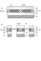
- FIG. 4A is a schematic cross-sectional view of the phase change film 40 for representing the effect of the first specific example.
- the phase change film 40 has a high nitrogen concentration portion 44 inside on the main surface and a low nitrogen concentration portion 42 outside on the main surface.
- the resistivity of the low nitrogen concentration portion 42 is high nitrogen concentration regardless of whether the low nitrogen concentration portion 42 is in a crystalline state or an amorphous state. It becomes lower than the resistivity of the portion 44. Accordingly, it is possible to preferentially flow current through the low nitrogen concentration portion 42, and hardly flow current through the high nitrogen concentration portion 44. As a result, it is possible to cause a current to flow preferentially through the low nitrogen concentration portion 42 and change only the low nitrogen concentration portion 42.
- the phase of the low nitrogen concentration portion 42 In order to change the phase of the low nitrogen concentration portion 42 from the crystalline state to the amorphous state, it is necessary to melt the low nitrogen concentration portion 42. In this case as well, a current pulse is preferentially applied only to the low nitrogen concentration portion 42. It is possible to change the phase to an amorphous state by flowing and locally melting only the low nitrogen concentration portion and quenching. That is, it is possible to change the phase of the low nitrogen concentration portion 42 from the crystalline state to the amorphous state and to change the phase from the amorphous state to the crystalline state while the high nitrogen concentration portion 44 is fixed in the amorphous state. Is possible. When the low nitrogen concentration portion 42 is melted, the temperature of the adjacent high nitrogen concentration portion 44 may rise to some extent.
- phase change (crystallization) temperature increases with the amount of nitrogen introduced. That is, by increasing the crystallization temperature of the high nitrogen concentration portion 44, it is possible to suppress crystallization of the high nitrogen concentration portion 44 even when the adjacent low nitrogen concentration portion 42 is heated.
- the high nitrogen concentration portion 44 is fixed in an amorphous state (the phase change from the amorphous state to the crystalline state is not caused), and the low nitrogen concentration portion 42 is formed. Only a phase change can be caused. That is, current can flow only in the low nitrogen concentration portion 42, and current can be prevented from flowing in the high nitrogen concentration portion 44.
- the amount of current flowing through the phase change film 40 is reduced and the power consumption is reduced as compared with the conventional phase change film having a uniform nitrogen concentration. It is done.
- FIG. 4B is a schematic cross-sectional view of the phase change film 40 for illustrating the effect of the second specific example.
- current can flow only in the low nitrogen concentration portion 42 and current can not flow in the high nitrogen concentration portion 44. That is, the specific example 2 also has the effect of reducing the amount of current flowing through the phase change film 40 and reducing the power consumption, compared to a conventional phase change film having a uniform nitrogen concentration.
- FIG. 5 is a schematic cross-sectional view of the phase change film 40 for explaining the effect of the second specific example.
- a phase change is caused in the low nitrogen concentration portion 42, and information is written and erased. Therefore, for stable operation, the current resistance characteristics and phase change temperature of the low nitrogen concentration portion 42 need to be within a predetermined range. However, if impurities are mixed in the low nitrogen concentration portion 42, the electrical resistance and the phase change temperature may fluctuate, and predetermined operating characteristics may not be obtained.
- the high nitrogen concentration portion 44 in which high concentration nitrogen is introduced is provided outside the low nitrogen concentration portion 42.
- the high nitrogen concentration portion 44 into which nitrogen is introduced at a high concentration serves as a protective wall, and impurities are less likely to enter the low nitrogen concentration portion 42 from the outside such as the inter-element insulating film. That is, according to the second specific example, an effect of preventing impurities from entering the low nitrogen concentration portion 42 of the phase change film 40 is also obtained.
- the yield decreases due to impurities entering the low nitrogen concentration portion 42 during the manufacturing process of the nonvolatile memory device, or the manufactured nonvolatile memory device is repeatedly written and erased in various environments. Even in such a case, it is possible to prevent fluctuations in operating characteristics due to diffusion of impurities into the low nitrogen concentration portion 42, and to improve long-term reliability.
- FIG. 6 is a process cross-sectional view illustrating an example of a method for manufacturing the nonvolatile memory device according to the first specific example.
- the rectifying element 20 is formed on the first wiring 10 (not shown).
- a first electrode 30 is formed on the rectifying element 20.
- a phase change film 40 containing nitrogen is formed on the first electrode 30.
- a second electrode 50 is formed on the phase change film 40.
- a second wiring 60 (not shown) is formed on the second electrode 50.
- the stacked body is patterned by etching or the like. Etching is performed to the depth of the interface between the first wiring 10 and the rectifying element 20. Thereafter, as shown in FIG. 6C, nitrogen is removed from the side surface of the phase change film 40. Examples of the removal method include annealing under reduced pressure or under vacuum. The side surface of the phase change film 40 is damaged by the etching described above. When annealing is performed under reduced pressure or vacuum in this state, nitrogen near the side surface of the phase change film 40 is released. As a result, the nitrogen concentration is relatively low outside the main surface of the phase change film 40.
- the high nitrogen concentration portion 44 is formed inside the main surface, and the low nitrogen concentration portion 42 is formed outside the main surface. It is also effective to modify the phase change film 40 by exposing the side surface of the phase change film 40 to, for example, a rare gas plasma or irradiating with an ion beam or an electron beam before annealing. A physical or chemical impact is applied to the side surface of the phase change film 40 by plasma, an electron beam, or the like, thereby changing the bonding state of elements in the vicinity of the side surface or introducing defects. As a result, nitrogen desorption can be promoted.
- FIG. 7 and 8 are process cross-sectional views illustrating another example of the manufacturing method according to the nonvolatile memory device of specific example 1.
- FIG. 7A the rectifying element 20 is formed on the first wiring 10 (not shown).
- a first electrode 30 is formed on the rectifying element 20.
- a phase change material film 48 not containing nitrogen is formed on the first electrode 30.
- a dummy mask 70 is formed on the phase change material film 48.
- nitrogen is introduced into the phase change material film 48 using the dummy mask 70 as a mask.
- the introduction method include an ion implantation method, a gas phase diffusion method, and a method using nitrogen plasma or nitrogen radical.
- the nonvolatile memory device according to the first specific example having the high nitrogen concentration portion 44 inside the main surface and the low nitrogen concentration portion 42 outside the main surface is manufactured.
- FIG. 9 is a process cross-sectional view illustrating an example of a manufacturing method according to the nonvolatile memory device of specific example 2.
- the rectifying element 20 is formed on the first wiring 10 (not shown).
- a first electrode 30 is formed on the rectifying element 20.
- a phase change film 40 containing nitrogen is formed on the first electrode 30.
- nitrogen is introduced by sputtering in a nitrogen atmosphere having a flow rate ratio (N 2 / Ar) of nitrogen gas to argon gas of 1 to 10%. be able to.
- a second electrode 50 is formed on the phase change film 40.
- a second wiring 60 (not shown) is formed on the second electrode 50.
- phase change film 40 is formed from the side surface of the phase change film 40.
- the introduction method include annealing in an atmosphere containing nitrogen gas, and exposure to nitrogen plasma, nitrogen radicals, and the like.
- the nitrogen concentration is relatively high.
- an inner low nitrogen concentration portion 42 within the main surface is formed, and a high nitrogen concentration portion 44 is formed outside the main surface.
- elements other than the phase change film 40 can be nitrided together.
- nitrogen may be introduced into the rectifying element 20 to obtain a predetermined rectifying characteristic.
- FIG. 10A the rectifying element 20 is formed on the first wiring 10 (not shown).
- a first electrode 30 is formed on the rectifying element 20.
- a phase change material film 48 not containing nitrogen is formed on the first electrode 30.
- a dummy mask 70 is formed on the phase change material film 48.
- nitrogen is introduced into the phase change material film 48 using the dummy mask 70 as a mask. Examples of the introduction method include ion implantation. As a result, a phase change film 40 having a high nitrogen concentration portion 44 having a relatively high nitrogen concentration and a low nitrogen concentration portion 42 having a relatively low nitrogen concentration is formed.
- the phase change film 40 has the low nitrogen concentration portion 42 on the inner side in the plane of the main surface and the high nitrogen concentration portion 44 on the outer side in the plane of the main surface. Is produced.
- phase change film 40 containing nitrogen is formed on the first electrode 30 in the step according to FIG. 9A, but the phase change material film 48 containing no nitrogen is formed. Also good.
- the phase change material film 48 that does not contain nitrogen is formed on the first electrode 30 in the steps according to FIGS. 7A and 10A.
- the phase change film 40 may be formed.
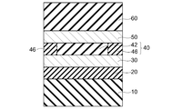
- FIG. 12 is a schematic cross-sectional view showing an example (specific example 3) of the nonvolatile memory device according to the third embodiment of the invention.
- the nonvolatile memory device of this example includes a first wiring 10, a rectifying element 20 provided on the first wiring 10, a first electrode 30 provided on the rectifying element 20, A phase change film 40 provided on one electrode 30; a second electrode 50 provided on the phase change film 40; and a second wiring 60 provided on the second electrode 50; .
- the phase change film 40 contains nitrogen in part or in part and oxygen in part, and a portion containing nitrogen at a relatively low concentration inside and not containing oxygen in the plane of the main surface ( It has a low nitrogen concentration portion 42), and a portion containing nitrogen at a relatively high concentration and containing oxygen (nitrogen oxygen introduction portion 46) outside the main surface.
- phase change film 40 in order to efficiently heat the phase change film 40 during the erase operation, for example, a resistivity of about 10 ⁇ 5 ⁇ cm or more is provided on the first electrode 30 side or the second electrode 50 side.
- a heater layer (not shown) made of the above material may be provided.
- the constituent materials of the rectifying element 20, the first electrode 30, the second electrode 50, and the phase change film 40 can be the same as those described above with respect to the first embodiment.
- phase change film 40 contains oxygen partially (outside in the main surface).
- Specific Example 3 can be the same as Specific Example 2 except that oxygen is introduced outside in the plane of the main surface of phase change film 40.
- phase change nonvolatile memory device by using the nitrogen concentration distribution in the in-plane direction of the main surface of the phase change film 40, power consumption is reduced and protection against impurities intrusion is achieved. A wall effect is obtained.
- oxygen is introduced into the phase change film 40 in addition to nitrogen.
- this example also has an effect of reducing the amount of current flowing through the phase change film 40 and reducing power consumption.
- the resistivity and phase change temperature of the nitrogen oxygen introduction portion 46 can be made higher than the resistivity and phase change temperature of the high nitrogen concentration portion 44 in the case of the specific example 2. .
- the effect of reducing power consumption is further increased.
- the current flowing through the nitrogen-oxygen introduction portion 46 can be further suppressed, and crystallization can be further suppressed.
- the phase of the low nitrogen concentration portion 42 can be stably changed, and the allowable range of current conditions for writing, erasing, and reading can be expanded.
- the nitrogen / oxygen introduction portion 46 serves as a protective wall, and the effect can be equal to or higher than the second specific example.
- FIG. 13 is a process cross-sectional view illustrating an example of a method for manufacturing the nonvolatile memory device according to the third specific example.
- the rectifying element 20 is formed on the first wiring 10 (not shown).
- a first electrode 30 is formed on the rectifying element 20.
- a phase change film 40 containing nitrogen is formed on the first electrode 30.
- nitrogen is introduced by sputtering in a nitrogen atmosphere having a flow rate ratio (N 2 / Ar) of nitrogen gas to argon gas of 1 to 10%. be able to.
- a second electrode 50 is formed on the phase change film 40.
- a second wiring 60 (not shown) is formed on the second electrode 50.
- patterning is performed by etching or the like. Etching is performed to the depth of the interface between the first wiring 10 and the rectifying element 20.
- nitrogen and oxygen are introduced from the side surface of the phase change film 40. Examples of the introduction method include nitriding treatment and oxidation treatment for the entire element including the first wiring 10 and the second wiring 60.
- the order of introducing nitrogen and oxygen does not matter. First, oxygen may be introduced after introducing nitrogen, nitrogen may be introduced after introducing oxygen, or both may be introduced simultaneously.
- the oxidation treatment may be annealing in an atmosphere containing oxygen, oxygen plasma treatment, or oxygen radical treatment. Further, this oxidation treatment may be used in combination with an oxidation treatment performed for repairing the rectifying element 20 damaged by patterning.
- the rectifying device 20 the use of CuInO 2, ZnInO 2 such oxides diode, the side wall portion of the rectifying element 20 in the patterning process shown in FIG. 13 (b) may be damaged.
- oxidation treatment can be performed to repair the damaged side wall portion of the rectifying element 20. Oxygen can be introduced from the side surface of the phase change film 40 during the oxidation treatment for repairing the rectifying element 20.
- the nitrogen concentration is relatively increased and oxygen is introduced outside the main surface of the phase change film 40.
- the low nitrogen concentration portion 42 is formed inside the main surface, and the nitrogen-oxygen introduction portion 46 is formed outside the main surface.
- FIG. 14 and 15 are process cross-sectional views illustrating another example of the manufacturing method according to the nonvolatile memory device of specific example 3.
- the rectifying element 20 is formed on the first wiring 10 (not shown).
- a first electrode 30 is formed on the rectifying element 20.
- a phase change film 40 containing nitrogen is formed on the first electrode 30.
- nitrogen is introduced by sputtering in a nitrogen atmosphere having a flow rate ratio (N 2 / Ar) of nitrogen gas to argon gas of 1 to 10%. Can do.
- a dummy mask 70 is formed on the phase change film 40.
- nitrogen and oxygen are introduced into the phase change film 40 using the dummy mask 70 as a mask.
- the introduction method include an ion implantation method, a gas phase diffusion method, a method using plasma and radicals, and the like.
- the order of introducing nitrogen and oxygen does not matter. First, oxygen may be introduced after introducing nitrogen, nitrogen may be introduced after introducing oxygen, or both may be introduced simultaneously.
- a nitrogen-oxygen-introducing portion 46 into which oxygen is introduced with a relatively high nitrogen concentration and a low nitrogen concentration portion 42 with a relatively low nitrogen concentration are formed.
- the dummy mask 70 is removed. Thereafter, the second electrode 50 is formed on the phase change film 40. Thereafter, a second wiring 60 (not shown) is formed on the second electrode 50.
- phase change film 40 has the low nitrogen concentration portion 42 on the inner side in the plane of the main surface and the nitrogen oxygen introduction portion 46 on the outer side in the plane of the main surface. Is produced.
- the phase change film 40 containing nitrogen is formed on the first electrode 30 in the steps shown in FIGS. 13A and 14A.
- the phase change material does not contain nitrogen.
- the film 48 may be formed.
- FIG. 16 is a schematic view illustrating a nonvolatile memory device according to the fifth embodiment of the invention.
- the inter-element isolation insulating film is omitted.
- a strip-shaped first wiring 110 extending in the X-axis direction is provided on the main surface 106 of the substrate 105.
- a band-like second wiring 120 extending in the Y-axis direction orthogonal to the X-axis in a plane parallel to the substrate 105 is provided to face the first wiring 110.
- a storage unit 200 made of a phase change film is sandwiched between the first wiring 110 and the second wiring 120. That is, in the nonvolatile memory device 2, the storage unit 200 is provided at a portion (cross point) where the first wiring 110 and the second wiring 120 intersect. This is a so-called cross-point cell array structure.
- the voltage applied to each storage unit 200 changes depending on the combination of the potential applied to the first wiring 110 and the potential applied to the second wiring 120, and the characteristics of the storage unit 200 at that time, that is, the resistance value (amorphous) Information can be stored or erased depending on the state of the high resistance state or the low resistance state of the crystalline state.
- a rectifying element unit 140 made of, for example, a diode is provided. be able to.
- FIG. 16 illustrates an example in which the rectifying element unit 140 is provided between the first wiring 110 and the storage unit 200, but the rectifying element unit 140 is provided between the second wiring 120 and the storage unit 200. It may be provided. Further, the rectifying element portion 140 may be provided in a region other than a region where the first wiring 110 and the second wiring 120 face each other.
- An electrode (not shown) can be provided between the rectifying element unit 140 and the storage unit 200 and between the storage unit 200 and the second wiring 120. This electrode also serves as a protective film.
- One storage section 200 (and rectifying element section 140) provided in a region where one first wiring 110 and one second wiring 120 cross each other is one element, which is referred to as a “cell”.
- the storage unit 200 made of a phase change film can have a low nitrogen concentration portion and a high nitrogen concentration portion in the in-plane direction of the main surface.
- the nonvolatile memory device of this embodiment has the effect described in the description of the first embodiment, that is, the effect of a protective wall against the reduction of power consumption and the entry of impurities.
- the storage unit 200 made of a phase change film can have a low nitrogen concentration portion and a nitrogen oxygen introduction portion in the main surface direction.
- the nonvolatile memory device of this embodiment has the effects described in the description of the third embodiment, that is, the effect of a protective wall against the reduction of power consumption and the entry of impurities.
- FIG. 16 illustrates an example in which three first wirings 110 and three second wirings 120 are provided, but the present invention is not limited to this, and the first wiring 110 and the second wiring 120 are not limited thereto.
- the number of wirings 120 is arbitrary.
- the first wiring 110 is referred to as a bit wiring (BL), and the second wiring 120 is referred to as a word line (WL).
- the first wiring 110 may be a word line (WL) and the second wiring 120 may be a bit line (BL).
- FIG. 17 is a schematic perspective view illustrating another example of the configuration of the nonvolatile memory device according to the fifth embodiment of the present invention.
- the memory unit 200 has a two-layer structure. That is, the nonvolatile memory device 4 is provided to face the substrate 105, the first wiring 110a in the first layer provided on the main surface 106 of the substrate 105, and the first wiring 110a in the first layer. A first-layer second wiring 120a, and a first-layer storage portion 200a sandwiched between the first-layer first wiring 110a and the first-layer second wiring 120a. These become the first-layer nonvolatile memory device 2a.
- the second wiring 120a in the first layer is used as the first wiring 110b in the second layer, the second layer storage unit 200b is provided thereon, and the second wiring 120b in the second layer is provided thereon. Is provided. These become the second-layer nonvolatile memory device 2b. Each layer is provided with switch element portions 140a and 140b.
- the storage unit 200 formed of each phase change film may have a low nitrogen concentration portion and a high nitrogen concentration portion, or a low nitrogen concentration portion and a nitrogen oxygen introduction portion.
- each effect mentioned above regarding FIG. 16 is acquired.
- the second wiring 120 a in the first layer and the first wiring 110 b in the second layer are respectively It is provided separately.
- the storage unit 200 made of the respective phase change films can have a low nitrogen concentration portion and a high nitrogen concentration portion, or a low nitrogen concentration portion and a nitrogen oxygen introduction portion. Also in this case, the effects described above with reference to FIG. 16 can be obtained.
- FIG. 17 and 18 illustrate the case where the storage unit 200 is stacked in two layers, three or more layers may be used.
- recording, erasing, and reproducing operations of the nonvolatile memory device according to the third embodiment of the present invention will be described with reference to FIG.
- the initial state (state in which no information is stored) of the storage unit 200 may be either a crystalline state (low resistance state) or an amorphous state (high resistance state).
- a case where the initial state of the storage unit 200 is an amorphous state (high resistance state) will be taken up.
- Recording (writing) of information in the storage unit 200 is performed by applying a voltage to the storage unit 200 and flowing a current pulse. For this reason, for example, a state in which the potential of the first wiring 110 is relatively lower than the potential of the second wiring 120 is created. If the second wiring 120 is set to a ground potential, for example, a negative potential may be applied to the first wiring 110. At this time, the current pulse preferentially flows through the low nitrogen concentration portion 42 described above.
- the low nitrogen concentration portion 42 of the storage unit 200 is heated to a temperature higher than the crystallization temperature due to Joule heat generated at this time. This temperature is maintained for a certain period of time, for example, less than 1 microsecond. Then, the memory
- all the first wirings 110 and all the second wirings 120 be precharged immediately before recording (writing) (during standby). Precharging is to keep the potential of each wiring constant in order to ensure good operating characteristics.
- the voltage pulse for recording may be generated by making the potential of the first wiring 110 higher than the potential of the second wiring 120.
- Erasing is performed by applying a large current pulse to the storage unit 200 and using Joule heat generated at this time. Also at this time, a current pulse preferentially flows through the low nitrogen concentration portion 42. Due to this Joule heat, the low nitrogen concentration portion 42 of the storage unit 200 is heated to a melting point (in the case of Ge 2 Sb 2 Te 5 , the melting point is 633 ° C.) or more. Thereafter, the storage unit 200 is rapidly cooled, for example, in a time shorter than 100 ns, and the phase of the low nitrogen concentration portion 42 is changed to an amorphous state. Thereby, information is erased. At this time, almost no current flows in the high nitrogen concentration portion 44 adjacent to the low nitrogen concentration portion 42 and the crystallization temperature is high. Therefore, when the low nitrogen concentration portion 42 is rapidly cooled after heating, it melts. And crystallization can be prevented.
- Reproduction is performed by applying a voltage to the storage unit 200 to flow a current pulse and detecting the resistance value at this time.
- the voltage pulse has a minute amplitude such that the material constituting the storage unit 200 does not cause a phase change.
- the resistance value of the storage unit 200 can be measured using a reading circuit.
- the read current generated from the read circuit flows to the storage unit 200 through the second wiring 120, and the resistance value of the storage unit 200 is measured by the read circuit.
- the low nitrogen concentration portion 42 is made crystalline or amorphous by writing / erasing, while the high nitrogen concentration portion 44 is always maintained in an amorphous state. Therefore, information can be reproduced by detecting a change in the resistance of the low nitrogen concentration portion 42.
- a current pulse can be preferentially passed through the low nitrogen concentration portion 42, and almost no current can be passed through the high nitrogen concentration portion 44. As a result, power consumption can be reduced.
- Such a non-volatile memory device can realize higher recording density and lower power consumption than conventional non-volatile memory devices using currently used hard disks and transistors.
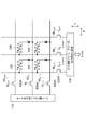
- FIG. 19 is a schematic diagram illustrating a circuit of the nonvolatile memory device illustrated in FIG. 16.
- BL represents a bit line
- WL represents a word line.
- the word lines WL i ⁇ 1 , WL i , WL i + 1 extend in the X direction
- the bit lines BL j ⁇ 1 , BL j , BL j + 1 extend in the Y direction.
- each of the word lines WL i ⁇ 1 , WL i , WL i + 1 is connected to a word line driver and decoder 115 via a MOS transistor RSW (Row Switch) as a selection switch, and a bit line BL j ⁇ 1 , BL j, one end of the BL j + 1 is, MOS transistor CSW as a selection switch (column switch: column switch) bit line driver via is connected decoder, and read circuit 125.
- MOS transistor RSW Row Switch
- Selection signals R i ⁇ 1 , R i , and R i + 1 for selecting one word line (Row) are input to the gate of the MOS transistor RSW, and 1 to the gate of the MOS transistor CSW.
- Selection signals C j ⁇ 1 , C j , and C j + 1 for selecting one bit line (Column: column) are input.
- the storage unit 200, the word lines WL i-1, WL i, WL i + 1 and the bit lines BL j-1, BL j, are arranged in the intersection of BL j + 1.
- a rectifying element unit 140 is added to the storage unit 200.
- the cross-point type nonvolatile memory device of this specific example does not require individual connection of a MOS transistor to the memory portion of each cell and can be multi-layered. It is advantageous.
- a nonvolatile memory device including a phase change film containing a material that changes between a crystalline state and an amorphous state by applying a voltage
- the nonvolatile power consumption can be reduced.
- a storage device and a manufacturing method thereof are provided.
Landscapes
- Engineering & Computer Science (AREA)
- Manufacturing & Machinery (AREA)
- Semiconductor Memories (AREA)
Abstract
La présente invention concerne un dispositif de mémoire non volatile comportant une première couche, une deuxième couche et une couche d'enregistrement qui est intercalée entre la première couche et la deuxième couche, et qui peut passer de manière réversible d'un premier état dans lequel la résistance est faible à un second état dans lequel la résistance est élevée, par un courant fourni par l'intermédiaire de la première couche et de la deuxième couche. La couche d'enregistrement présente une première partie et une seconde partie dont la teneur en azote est relativement supérieure à celle de la première partie dans une face principale du dispositif de mémoire non volatile. La présente invention concerne également un dispositif d'enregistrement/de reproduction d'informations non volatiles consommant peu d'énergie.
Priority Applications (3)
| Application Number | Priority Date | Filing Date | Title |
|---|---|---|---|
| JP2009554146A JPWO2009104239A1 (ja) | 2008-02-18 | 2008-02-18 | 不揮発性記憶装置及びその製造方法 |
| PCT/JP2008/052636 WO2009104239A1 (fr) | 2008-02-18 | 2008-02-18 | Dispositif de mémoire non volatile et son procédé de fabrication |
| US12/858,975 US8237145B2 (en) | 2008-02-18 | 2010-08-18 | Nonvolatile memory device with recording layer having two portions of different nitrogen amounts |
Applications Claiming Priority (1)
| Application Number | Priority Date | Filing Date | Title |
|---|---|---|---|
| PCT/JP2008/052636 WO2009104239A1 (fr) | 2008-02-18 | 2008-02-18 | Dispositif de mémoire non volatile et son procédé de fabrication |
Related Child Applications (1)
| Application Number | Title | Priority Date | Filing Date |
|---|---|---|---|
| US12/858,975 Continuation US8237145B2 (en) | 2008-02-18 | 2010-08-18 | Nonvolatile memory device with recording layer having two portions of different nitrogen amounts |
Publications (1)
| Publication Number | Publication Date |
|---|---|
| WO2009104239A1 true WO2009104239A1 (fr) | 2009-08-27 |
Family
ID=40985134
Family Applications (1)
| Application Number | Title | Priority Date | Filing Date |
|---|---|---|---|
| PCT/JP2008/052636 Ceased WO2009104239A1 (fr) | 2008-02-18 | 2008-02-18 | Dispositif de mémoire non volatile et son procédé de fabrication |
Country Status (3)
| Country | Link |
|---|---|
| US (1) | US8237145B2 (fr) |
| JP (1) | JPWO2009104239A1 (fr) |
| WO (1) | WO2009104239A1 (fr) |
Cited By (1)
| Publication number | Priority date | Publication date | Assignee | Title |
|---|---|---|---|---|
| KR20140136192A (ko) * | 2013-05-20 | 2014-11-28 | 에스케이하이닉스 주식회사 | 반도체 장치 및 그 제조 방법, 이 반도체 장치를 포함하는 마이크로 프로세서, 프로세서, 시스템, 데이터 저장 시스템 및 메모리 시스템 |
Families Citing this family (8)
| Publication number | Priority date | Publication date | Assignee | Title |
|---|---|---|---|---|
| US8565003B2 (en) * | 2011-06-28 | 2013-10-22 | Unity Semiconductor Corporation | Multilayer cross-point memory array having reduced disturb susceptibility |
| US20130082232A1 (en) | 2011-09-30 | 2013-04-04 | Unity Semiconductor Corporation | Multi Layered Conductive Metal Oxide Structures And Methods For Facilitating Enhanced Performance Characteristics Of Two Terminal Memory Cells |
| WO2009122570A1 (fr) * | 2008-04-01 | 2009-10-08 | 株式会社 東芝 | Dispositif d'enregistrement et de reproduction d'informations |
| WO2009128142A1 (fr) * | 2008-04-15 | 2009-10-22 | 株式会社 東芝 | Appareil d’enregistrement et de lecture d’informations |
| US9054295B2 (en) | 2011-08-23 | 2015-06-09 | Micron Technology, Inc. | Phase change memory cells including nitrogenated carbon materials, methods of forming the same, and phase change memory devices including nitrogenated carbon materials |
| JP5840505B2 (ja) * | 2012-01-12 | 2016-01-06 | 株式会社東芝 | 半導体装置の製造方法 |
| KR20150145631A (ko) * | 2014-06-20 | 2015-12-30 | 에스케이하이닉스 주식회사 | 크로스 포인트 어레이를 구비하는 반도체 장치의 제조 방법 |
| US12402546B2 (en) * | 2021-12-28 | 2025-08-26 | International Business Machines Corporation | Composite material phase change memory cell |
Citations (4)
| Publication number | Priority date | Publication date | Assignee | Title |
|---|---|---|---|---|
| JP2005032855A (ja) * | 2003-07-09 | 2005-02-03 | Matsushita Electric Ind Co Ltd | 半導体記憶装置及びその製造方法 |
| JP2006156886A (ja) * | 2004-12-01 | 2006-06-15 | Renesas Technology Corp | 半導体集積回路装置およびその製造方法 |
| JP2007035683A (ja) * | 2005-07-22 | 2007-02-08 | Elpida Memory Inc | 半導体装置及びその製造方法 |
| JP2007235142A (ja) * | 2006-03-02 | 2007-09-13 | Samsung Electronics Co Ltd | 不揮発性メモリ素子及びそれを備えるメモリアレイ |
Family Cites Families (3)
| Publication number | Priority date | Publication date | Assignee | Title |
|---|---|---|---|---|
| US7524612B2 (en) * | 2002-06-03 | 2009-04-28 | Pioneer Corporation | Information recording medium and process for producing the same |
| US7218484B2 (en) * | 2002-09-11 | 2007-05-15 | Kabushiki Kaisha Toshiba | Magnetoresistance effect element, magnetic head, and magnetic reproducing apparatus |
| JP4357454B2 (ja) * | 2005-06-08 | 2009-11-04 | 株式会社東芝 | 光記録媒体および光ディスク |
-
2008
- 2008-02-18 WO PCT/JP2008/052636 patent/WO2009104239A1/fr not_active Ceased
- 2008-02-18 JP JP2009554146A patent/JPWO2009104239A1/ja active Pending
-
2010
- 2010-08-18 US US12/858,975 patent/US8237145B2/en active Active
Patent Citations (4)
| Publication number | Priority date | Publication date | Assignee | Title |
|---|---|---|---|---|
| JP2005032855A (ja) * | 2003-07-09 | 2005-02-03 | Matsushita Electric Ind Co Ltd | 半導体記憶装置及びその製造方法 |
| JP2006156886A (ja) * | 2004-12-01 | 2006-06-15 | Renesas Technology Corp | 半導体集積回路装置およびその製造方法 |
| JP2007035683A (ja) * | 2005-07-22 | 2007-02-08 | Elpida Memory Inc | 半導体装置及びその製造方法 |
| JP2007235142A (ja) * | 2006-03-02 | 2007-09-13 | Samsung Electronics Co Ltd | 不揮発性メモリ素子及びそれを備えるメモリアレイ |
Cited By (2)
| Publication number | Priority date | Publication date | Assignee | Title |
|---|---|---|---|---|
| KR20140136192A (ko) * | 2013-05-20 | 2014-11-28 | 에스케이하이닉스 주식회사 | 반도체 장치 및 그 제조 방법, 이 반도체 장치를 포함하는 마이크로 프로세서, 프로세서, 시스템, 데이터 저장 시스템 및 메모리 시스템 |
| KR102029908B1 (ko) * | 2013-05-20 | 2019-10-08 | 에스케이하이닉스 주식회사 | 반도체 장치 및 그 제조 방법, 이 반도체 장치를 포함하는 마이크로 프로세서, 프로세서, 시스템, 데이터 저장 시스템 및 메모리 시스템 |
Also Published As
| Publication number | Publication date |
|---|---|
| US8237145B2 (en) | 2012-08-07 |
| JPWO2009104239A1 (ja) | 2011-06-16 |
| US20110024713A1 (en) | 2011-02-03 |
Similar Documents
| Publication | Publication Date | Title |
|---|---|---|
| US8237145B2 (en) | Nonvolatile memory device with recording layer having two portions of different nitrogen amounts | |
| JP6151650B2 (ja) | 記憶装置 | |
| JP4995834B2 (ja) | 半導体記憶装置 | |
| JP6772124B2 (ja) | スイッチ素子および記憶装置 | |
| US9040949B2 (en) | Information recording device and method of manufacturing the same | |
| JP4792007B2 (ja) | 情報記録再生装置 | |
| JP4577693B2 (ja) | 不揮発性メモリ素子及びその製造方法 | |
| JP4792006B2 (ja) | 情報記録再生装置 | |
| JPWO2008142768A1 (ja) | 半導体装置およびその製造方法 | |
| JP2015135917A5 (fr) | ||
| WO2010026923A1 (fr) | Elément de stockage et dispositif de stockage | |
| TW200807776A (en) | Semiconductor memory devices | |
| JP6050015B2 (ja) | 記憶素子および記憶装置 | |
| WO2009122569A1 (fr) | Dispositif d'enregistrement et de reproduction d'informations | |
| TW200839765A (en) | Information recording/reproducing device | |
| JP5225372B2 (ja) | 情報記録再生装置 | |
| JP4465969B2 (ja) | 半導体記憶素子及びこれを用いた半導体記憶装置 | |
| JP2008084512A (ja) | 情報記録再生装置 | |
| JP4577692B2 (ja) | 不揮発性メモリ素子及びその製造方法 | |
| JP5007502B2 (ja) | 記憶素子の製造方法 | |
| TWI406407B (zh) | Information recording and reproducing device | |
| TWI396281B (zh) | Information recording and reproducing device | |
| JP5103470B2 (ja) | 半導体装置およびその製造方法 | |
| WO2009116139A1 (fr) | Dispositif d'enregistrement/reproduction d'informations | |
| JPWO2008129684A1 (ja) | 情報記録再生装置 |
Legal Events
| Date | Code | Title | Description |
|---|---|---|---|
| 121 | Ep: the epo has been informed by wipo that ep was designated in this application |
Ref document number: 08711460 Country of ref document: EP Kind code of ref document: A1 |
|
| WWE | Wipo information: entry into national phase |
Ref document number: 2009554146 Country of ref document: JP |
|
| NENP | Non-entry into the national phase |
Ref country code: DE |
|
| 122 | Ep: pct application non-entry in european phase |
Ref document number: 08711460 Country of ref document: EP Kind code of ref document: A1 |