WO2009104533A1 - Dispositif de croissance de monocristaux de silicium et creuset en quartz - Google Patents
Dispositif de croissance de monocristaux de silicium et creuset en quartz Download PDFInfo
- Publication number
- WO2009104533A1 WO2009104533A1 PCT/JP2009/052485 JP2009052485W WO2009104533A1 WO 2009104533 A1 WO2009104533 A1 WO 2009104533A1 JP 2009052485 W JP2009052485 W JP 2009052485W WO 2009104533 A1 WO2009104533 A1 WO 2009104533A1
- Authority
- WO
- WIPO (PCT)
- Prior art keywords
- single crystal
- silicon single
- quartz crucible
- diameter
- peripheral wall
- Prior art date
- Legal status (The legal status is an assumption and is not a legal conclusion. Google has not performed a legal analysis and makes no representation as to the accuracy of the status listed.)
- Ceased
Links
Images

Classifications
-
- C—CHEMISTRY; METALLURGY
- C30—CRYSTAL GROWTH
- C30B—SINGLE-CRYSTAL GROWTH; UNIDIRECTIONAL SOLIDIFICATION OF EUTECTIC MATERIAL OR UNIDIRECTIONAL DEMIXING OF EUTECTOID MATERIAL; REFINING BY ZONE-MELTING OF MATERIAL; PRODUCTION OF A HOMOGENEOUS POLYCRYSTALLINE MATERIAL WITH DEFINED STRUCTURE; SINGLE CRYSTALS OR HOMOGENEOUS POLYCRYSTALLINE MATERIAL WITH DEFINED STRUCTURE; AFTER-TREATMENT OF SINGLE CRYSTALS OR A HOMOGENEOUS POLYCRYSTALLINE MATERIAL WITH DEFINED STRUCTURE; APPARATUS THEREFOR
- C30B29/00—Single crystals or homogeneous polycrystalline material with defined structure characterised by the material or by their shape
- C30B29/02—Elements
- C30B29/06—Silicon
-
- C—CHEMISTRY; METALLURGY
- C30—CRYSTAL GROWTH
- C30B—SINGLE-CRYSTAL GROWTH; UNIDIRECTIONAL SOLIDIFICATION OF EUTECTIC MATERIAL OR UNIDIRECTIONAL DEMIXING OF EUTECTOID MATERIAL; REFINING BY ZONE-MELTING OF MATERIAL; PRODUCTION OF A HOMOGENEOUS POLYCRYSTALLINE MATERIAL WITH DEFINED STRUCTURE; SINGLE CRYSTALS OR HOMOGENEOUS POLYCRYSTALLINE MATERIAL WITH DEFINED STRUCTURE; AFTER-TREATMENT OF SINGLE CRYSTALS OR A HOMOGENEOUS POLYCRYSTALLINE MATERIAL WITH DEFINED STRUCTURE; APPARATUS THEREFOR
- C30B15/00—Single-crystal growth by pulling from a melt, e.g. Czochralski method
- C30B15/10—Crucibles or containers for supporting the melt
-
- C—CHEMISTRY; METALLURGY
- C30—CRYSTAL GROWTH
- C30B—SINGLE-CRYSTAL GROWTH; UNIDIRECTIONAL SOLIDIFICATION OF EUTECTIC MATERIAL OR UNIDIRECTIONAL DEMIXING OF EUTECTOID MATERIAL; REFINING BY ZONE-MELTING OF MATERIAL; PRODUCTION OF A HOMOGENEOUS POLYCRYSTALLINE MATERIAL WITH DEFINED STRUCTURE; SINGLE CRYSTALS OR HOMOGENEOUS POLYCRYSTALLINE MATERIAL WITH DEFINED STRUCTURE; AFTER-TREATMENT OF SINGLE CRYSTALS OR A HOMOGENEOUS POLYCRYSTALLINE MATERIAL WITH DEFINED STRUCTURE; APPARATUS THEREFOR
- C30B15/00—Single-crystal growth by pulling from a melt, e.g. Czochralski method
- C30B15/20—Controlling or regulating
- C30B15/22—Stabilisation or shape controlling of the molten zone near the pulled crystal; Controlling the section of the crystal
- C30B15/26—Stabilisation or shape controlling of the molten zone near the pulled crystal; Controlling the section of the crystal using television detectors; using photo or X-ray detectors
Definitions
- the present invention relates to a silicon single crystal growth apparatus and a quartz crucible, and more particularly to a silicon single crystal growth apparatus and a quartz crucible capable of growing a silicon single crystal for a silicon wafer having a diameter of 450 mm.
- Non-Patent Document 1 As an apparatus for producing a silicon single crystal by the Czochralski method (CZ method), for example, those described in Patent Document 1 and Non-Patent Document 1 are known. That is, a solid crystal silicon raw material is heated and melted in a quartz crucible to form a melt (silicon melt), and then the seed crystal is immersed in the melt and pulled up while rotating, and below the seed crystal. This is a device for growing a silicon single crystal. In a crystal growth method using a general silicon single crystal growth apparatus, first, the silicon single crystal is increased in diameter (increased portion) to a predetermined diameter larger than the diameter of the seed crystal through the neck portion.
- CZ method Czochralski method
- a straight body portion (body portion) having a substantially constant diameter is formed by a predetermined length continuously with the increased diameter portion.
- a reduced diameter part is formed continuously to the straight body part, and the silicon single crystal is separated from the melt.
- the neck portion is a portion for removing dislocations introduced when the seed crystal is immersed in the melt.
- the diameter-reduced portion is a portion that prevents dislocation due to a rapid temperature change when the growing silicon single crystal is separated from the melt.
- a silicon single crystal is manufactured through the above steps.
- the straight body portion of the obtained silicon single crystal is subjected to peripheral grinding, block cutting, slicing, and polishing in sequence to obtain a large number of silicon wafers. Thereafter, heat treatment, epitaxial growth, and the like are performed as necessary, and a silicon wafer that is a material of the semiconductor device is manufactured.
- the amount of the melt remaining in the quartz crucible in a small amount can be made substantially constant regardless of the length of the straight body portion (the amount of melt formed first in the quartz crucible). Therefore, when the weight ratio of the silicon block to the silicon raw material for crystal is taken as the yield, the yield can be increased by increasing the amount of the melt first formed in the quartz crucible and growing the silicon single crystal having a long straight body. Rise. In recent years, an increase in the diameter of a silicon single crystal has been promoted, and a silicon single crystal for a silicon wafer having a diameter of 300 mm has been manufactured, and a silicon single crystal for a silicon wafer having a diameter of 450 mm has also been manufactured (non- Patent Document 1).
- the graph of FIG. 4 shows a change in yield with respect to the diameter of the straight body portion when the shapes of the increased diameter portion and the reduced diameter portion are similar to the diameter.
- a quartz crucible whose diameter and height (depth) increase proportionally with the increase in the straight body of a silicon single crystal can be used regardless of the diameter of the straight body.
- a silicon single crystal can be grown with substantially the same yield.
- the quartz crucible used in the Czochralski method has an outer diameter of the peripheral wall portion of about 2.5 to 3 times the diameter of the straight body portion of the silicon single crystal.
- the depth (height) and inner diameter of the quartz crucible are proportional to the outer diameter of the quartz crucible.
- a quartz crucible having a similar shape as described above can be used.
- the diameter of a quartz crucible that can be used (manufactured) is 45 inches or less. That is, since the quartz crucible exceeding 45 inches is large, the conventional crucible manufacturing apparatus cannot provide a sufficient amount of heat necessary for melting the quartz powder. Therefore, only those having inferior crucible quality can be manufactured as compared with the case of a quartz crucible used for growing a silicon single crystal for a silicon wafer having a diameter of 300 mm or less. As a result, it is difficult to obtain a quartz crucible exceeding 45 inches.
- a quartz crucible having an outer diameter not more than 2.5 times the diameter of the silicon single crystal has to be used.
- the silicon single crystal growth apparatus becomes extremely large, and there is a concern that the manufacturing method will be exceeded.
- the temperature of the quartz crucible becomes higher than that of the conventional quartz crucible, the quartz crucible is softened and deformed, and there is a possibility that the silicon single crystal growth becomes impossible in the middle.
- the depth of the quartz crucible is increased and the amount of the first melt formed is increased. Can be considered.
- the depth of the quartz crucible has a great influence on the following two points in each production process of a silicon single crystal by the Czochralski method.
- the diameter of the silicon single crystal is controlled by controlling the diameter and pulling speed of the silicon single crystal according to a preset profile.
- a measurement method a method is known in which the weight of a silicon single crystal is measured with a load cell or the like, and the diameter of the silicon single crystal is calculated from the change in weight at this time.
- a method for optically measuring the diameter of a silicon single crystal with a CCD camera or the like is also known.
- a silicon single crystal having a diameter of 450 mm or more is heavy. As a result, sufficient measurement accuracy cannot be obtained by the method of calculating the diameter of the silicon single crystal from the measured value in a load cell or the like. Therefore, the optical measurement is essential.
- the angular position of the CCD camera is set with respect to the pulling center line (the axis of the pulling axis) of the silicon single crystal. It was necessary to incline 20 ° or more.
- a shielding body for preventing radiant heat from the peripheral wall portion of the quartz crucible, the heater on the outside thereof, and the heat insulating cylinder toward the silicon single crystal Therefore, if the quartz crucible is deep, it is necessary to install a high shield. As a result, the shield becomes an obstacle, and the setting of the angle of the CCD camera is hindered.
- a radiant heat shield is provided in the space surrounding the silicon single crystal.
- the shield is a cylinder that cools the silicon single crystal being pulled up more rapidly and reduces the change in the cooling pattern in the length direction.
- a high shield is installed to cover the space of the quartz crucible that rises when the quartz crucible is pulled up.
- the silicon single crystal is not cooled rapidly but gradually cooled by the thermal radiation of the silicon single crystal itself. Thereby, each desired size and each desired density cannot be obtained about a defect and a defect nucleus.
- the inventor has made the outer diameter of the quartz crucible 36 mm or more suitable for pulling up a silicon single crystal capable of forming a silicon wafer having a diameter of 450 mm, and the quartz crucible with respect to the diameter of the quartz crucible.
- the cooling pattern can be set to the same level as when a silicon single crystal (diameter 302 to 320 mm) capable of forming a silicon wafer having a diameter of 300 mm is pulled up. As a result, it was found that a high-quality silicon single crystal in which the defect size and defect density in the silicon single crystal were controlled was obtained, and the present invention was completed.
- This invention can secure a good imaging angle when measuring the diameter of a silicon single crystal with an optical camera.
- the cooling pattern of the silicon single crystal capable of forming a silicon wafer having a diameter of 450 mm during the pulling can be set to the same level as in the case of pulling up the silicon single crystal capable of forming a silicon wafer having a diameter of 300 mm.
- An object of the present invention is to provide a silicon single crystal growth apparatus and a quartz crucible that can simultaneously satisfy the above effects.
- a quartz crucible housed in a chamber is filled with a silicon raw material for crystal and melted, and the seed crystal immersed in the melt is pulled up while rotating, thereby lowering the seed crystal.
- a silicon single crystal growth apparatus for growing a silicon single crystal by the Czochralski method wherein the silicon single crystal has a straight body portion capable of forming a silicon wafer having a diameter of 450 mm, and an upper portion of the chamber
- An optical camera for imaging the silicon single crystal in the vicinity of the liquid surface of the melt is provided, and the quartz crucible has a peripheral wall portion whose outer diameter is constant over the entire length, and a bottom portion that closes an opening below the peripheral wall portion.
- the outer diameter of the peripheral wall is 36 inches or more, and the depth on the center line of the quartz crucible is 80% or less of the outer diameter of the peripheral wall.
- the outer diameter of the peripheral wall portion is 36 inches or more and the depth on the center line of the quartz crucible is the peripheral wall portion.
- the outer diameter was 80% or less.
- the center line for pulling up the silicon single crystal substantially overlaps the center line of the quartz crucible. Therefore, if the outer diameter of the peripheral wall portion is 36 inches (914.4 mm) or more, a cylindrical shape having a width of 200 mm or more is provided around the silicon single crystal in the radial direction of the quartz crucible, excluding the thickness of the quartz crucible. A space is formed.
- an inclination angle of 20 ° or more can be secured with respect to the pulling center line.
- This 20 ° or more is a good imaging angle of the silicon single crystal by the optical camera. This eliminates the possibility that, as the silicon single crystal grows, when the melt surface reaches the bottom region of the quartz crucible, the silicon single crystal cannot be measured by imaging the silicon single crystal with a camera. .
- the depth on the center line of the quartz crucible (height from the center of the inner surface of the bottom portion to the center of the upper surface where the peripheral wall portion is opened) is shallower than 80% of the outer diameter of the peripheral wall portion.
- the cooling effect of the portion immediately after pulling up the silicon single crystal is enhanced.
- the cooling pattern of the silicon single crystal for the 450 mm wafer being pulled can be improved to the same extent as in the case of pulling the silicon single crystal capable of forming a silicon wafer having a diameter of 300 mm.
- a high-quality silicon single crystal in which the defect size and defect density in the silicon single crystal are controlled can be obtained.
- a main chamber in which a quartz crucible is accommodated and a pull chamber having a smaller diameter than the main chamber can be used.
- the crystal silicon material solid polycrystalline silicon or the like can be employed.
- a dopant such as boron (B) or phosphorus (P) may be added to the melt.
- the shape of the silicon single crystal for example, one having a neck portion (drawing portion), an increased diameter portion (upward cone portion), a straight body portion, and a reduced diameter portion (downward cone portion) can be adopted. Moreover, the thing with almost no neck part and the thing without a reduced diameter part may be sufficient.
- the straight body part capable of forming a silicon wafer having a diameter of 450 mm does not have to be 450 mm in diameter, which is the same as the diameter of the silicon wafer, and includes a straight body part having a larger diameter, for example, a diameter of 451 to 480 mm. . That is, for the straight body portion of the silicon single crystal, peripheral grinding of about 0.5 to 15 mm is performed on the silicon block after the block cutting in the wafer processing step. Considering this, the diameter of the straight body portion of the silicon single crystal capable of forming a silicon wafer having a diameter of 450 mm is set to 451 to 480 mm.
- the Czochralski method not only a general CZ method but also a magnetic field application type Czochralski pulling method (MCZ method) in which a magnet is disposed around a quartz crucible may be employed.
- the quartz crucible includes a cylindrical peripheral wall portion whose outer diameter is constant over the entire length (a horizontal cross-sectional shape and a constant cross-sectional area), a bottom portion having a predetermined bulge shape or a flat shape, which is disposed below the peripheral wall portion.
- a shape in which the outer surface has a radius of curvature that is inseparably connected by a bulging corner portion that is smaller than the radius of curvature of the outer surface of the bottom can be employed.
- Another quartz crucible may be one in which the corner portion does not exist and the bottom portion is directly connected to the lower opening of the peripheral wall portion.
- Each maximum outer diameter of the corner part and the bottom part may be larger than the outer diameter of the peripheral wall part.
- the “bulging shape” refers to a shape bulging outward of the quartz crucible.
- the outer diameter of the quartz crucible is 36 inches or more. For example, 36 inches, 40 inches, 44 inches, and 48 inches may be used.
- the pulling length of the silicon single crystal (straight barrel portion) can be changed according to the amount of the melt formed in each size quartz crucible.
- the depth on the center line of the quartz crucible is 80% or less of the outer diameter of the peripheral wall portion. If it exceeds 80%, it becomes difficult to install a shielding member for radiant heat on the silicon single crystal and to set the imaging angle of the silicon single crystal by the optical camera to 20 ° or more. As a result, there is a possibility that the silicon single crystal cannot be measured by imaging the silicon single crystal with a camera. Moreover, if it exceeds 80%, the cooling pattern of the silicon single crystal being pulled will deviate from that of a silicon single crystal capable of forming a silicon wafer having a diameter of 300 mm.
- the preferred height of the quartz crucible is 50 to 80% of the outer diameter of the quartz crucible. If it is this range, the more suitable effect that it can respond also to what was set to the cooling higher than the cooling pattern of the silicon single crystal which can form a silicon wafer with a diameter of 300 mm will be acquired.
- a CCD camera can be used as the optical camera. The optical camera is disposed in the upper part of the external space of the chamber, and images the silicon single crystal through a viewing window installed in the chamber. The image of the silicon single crystal is sent to a diameter measuring means (diameter measuring circuit) of the image processing apparatus, and the diameter of the portion (near the meniscus) immediately after the silicon single crystal is pulled up is measured.
- the invention according to claim 2 is the silicon single crystal growth apparatus according to claim 1, wherein the depth of the quartz crucible on the center line is 50 to 80% of the outer diameter of the peripheral wall portion.
- the depth on the center line of the quartz crucible is less than 50% of the outer diameter of the peripheral wall portion, the depth of the quartz crucible becomes small. Therefore, the amount of the melt that can form a silicon single crystal is limited, and in order to compensate for this, a quartz crucible having a larger diameter must be used. As a result, the silicon single crystal device is further increased in size. On the other hand, if it exceeds 80%, it becomes difficult to set the imaging angle of the silicon single crystal by the optical camera to 20 ° or more.
- the silicon single crystal cannot be measured by imaging the silicon single crystal with a camera.
- the cooling pattern of the silicon single crystal being pulled deviates from that of the silicon single crystal for a 300 mm wafer. For this reason, it becomes difficult to control the defect size and defect density in the silicon single crystal, and a high-quality silicon single crystal cannot be obtained.
- the invention according to claim 3 has a peripheral wall portion whose outer diameter is constant over the entire length, and a bottom portion that closes the opening on the lower side of the peripheral wall portion, and can form a silicon wafer having a diameter of 450 mm by the Czochralski method.
- the invention according to claim 4 is the quartz crucible according to claim 3, wherein the depth on the center line of the quartz crucible is 50 to 80% of the outer diameter of the peripheral wall portion.
- a silicon single crystal having a straight body portion capable of forming a silicon wafer having a diameter of 450 mm is grown by the Czochralski method.
- the outer diameter of the peripheral wall portion of the quartz crucible is 36 inches or more, and the depth on the center line of the quartz crucible is 80% or less of the outer diameter of the peripheral wall portion.
- the cooling pattern of the silicon single crystal capable of forming a silicon wafer having a diameter of 450 mm during the pulling can be set to the same level as that of pulling up the silicon single crystal capable of forming a silicon wafer having a diameter of 300 mm.
- the occurrence frequency of dislocations in the silicon single crystal can be reduced, and a high quality silicon single crystal can be obtained.
- the depth on the center line of the quartz crucible is set to 50 to 80% of the outer diameter of the peripheral wall portion, a silicon single unit capable of forming a silicon wafer having a diameter of 300 mm is formed. It is possible to cope with a crystal cooling pattern set to a higher cooling.
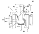
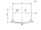
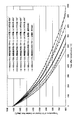
- FIG. 1 It is a block diagram of the silicon single crystal growth apparatus which concerns on Example 1 of this invention. It is a longitudinal cross-sectional view of the quartz crucible which concerns on Example 1 of this invention. It is the graph which compared the cooling pattern of the silicon single crystal which can form a silicon wafer whose diameter of a straight body part is 300 mm, and the silicon single crystal which can form a silicon wafer whose diameter of a direct body part is 450 mm. It is a graph which shows the relationship between the amount of initial stage silicon melts, and the yield of a silicon single crystal.
- reference numeral 10 denotes a silicon single crystal growth apparatus (hereinafter referred to as a crystal growth apparatus) according to Embodiment 1 of the present invention, and this crystal growth apparatus 10 includes a hollow cylindrical chamber 11.
- the chamber 11 includes a main chamber 12 and a pull chamber 13 that is continuously fixed on the main chamber 12 and has a smaller diameter than the main chamber 12.
- a crucible 14 is fixed on a support shaft (pedestal) 15 that can rotate and move up and down.
- the crucible 14 has a double structure in which an inner quartz crucible 16 and an outer graphite crucible 17 are combined.
- the quartz crucible 16 has a radius of curvature smaller than that of the outer surface of the bottom portion 19, with the peripheral wall portion 18 having a constant outer diameter a and the bulging bottom portion 19 disposed below the peripheral wall portion 18. It is connected inseparably by a corner portion 20 having a bulging outer surface (FIG. 2).
- the outer diameter a of the peripheral wall portion 18 is 36 inches (914.4 mm).
- the depth b on the central axis of the quartz crucible 16 is 80% of the outer diameter a of the peripheral wall portion 18.
- a resistance heating heater 21 is arranged concentrically with the peripheral wall 18.
- a cylindrical heat insulating cylinder 22 is disposed along the inner surface of the main chamber 12 outside the heater 21.
- a circular heat insulating plate 23 is disposed on the bottom surface of the main chamber 12.
- a pair of superconducting magnets 24 are opposed to each other outside the main chamber 12 in order to form a horizontal magnetic field.
- a pulling shaft (which can be a wire) 25 that can rotate and move up and down with the same axis as the support shaft 15 is suspended through the pull chamber 13.
- a seed crystal C is attached to the lower end of the pulling shaft 25.
- a CCD camera (optical camera) 30 that shoots the silicon single crystal S in the vicinity of the liquid level 26 a of the melt 26 through a window formed in the main chamber 12 is suspended from the outside of the main chamber 12.
- the diameter of the straight body portion S3 of the silicon single crystal S to be manufactured is 465 mm capable of forming a 450 mm silicon wafer.
- silicon raw material for crystal and boron as an impurity are charged into the crucible 14.
- the pressure inside the chamber 11 is reduced to 50 Torr, and 200 L / min Ar gas is introduced as an inert gas.
- the charge in the crucible 14 is melted by the heater 21 to form a melt 26 in the crucible 14.
- the amount of the melt 26 at this time (at the start of the growth of the silicon single crystal S) is such that the liquid surface 26 a exists in the region of the peripheral wall portion 18 of the quartz crucible 16.
- the seed crystal C attached to the lower end of the pulling shaft 25 is immersed in the melt 26, while the crucible 14 and the pulling shaft 25 are rotated in opposite directions, the pulling shaft 25 is pulled up in the axial direction, and the seed crystal C A silicon single crystal S is grown below the substrate.
- the vicinity of the liquid surface of the silicon single crystal S being pulled is always imaged by the CCD camera 30, and the diameter of the silicon single crystal S immediately after the pulling is determined by the diameter measuring means of an image processing apparatus (not shown) based on the image data. Always measured.
- dislocation is removed by a drawing process, and a neck portion S1 is formed.
- the increased diameter portion S2 is formed by the diameter increasing step subsequent to the drawing step, and the formation of the straight body portion S3 is started by stopping the diameter increase.
- the applied magnetic field strength, the rotational speed of the pulling shaft 25, and the rotational speed of the crucible 14 are respectively set so that the quality such as the presence / absence of magnetic field application and the oxygen concentration of the silicon single crystal S as a product becomes desired. Adjusted.
- the upward cone-shaped increased diameter portion S2 is formed by changing the speed.
- the diameter of the increased diameter portion S2 reaches a predetermined diameter (385 mm)
- the power of the heater 21 and the lifting speed of the pulling shaft 25 are further changed, and then the process proceeds to the straight body portion S3.
- the straight barrel portion S3 is formed by adjusting the rising speed of the lifting shaft 25.
- the crystal weight obtained by calculation from the diameter measuring means and the position detector of the crystal S (not shown) or the straight body length converted from the weight is set to a preset weight or a preset straight body length.
- the power of the heater 21 is adjusted.
- the diameter-decreasing portion of the downward cone shape is gradually formed, and finally the growth of the silicon single crystal S is completed at the apex of the downward cone.
- the outer wall a has an outer diameter a of 36 inches and a depth on the center line of the quartz crucible 16. Since the thickness b is 80% of the outer diameter a, a good imaging angle when measuring the diameter of the silicon single crystal S by the CCD camera 30 can be secured.
- the cooling pattern of the silicon single crystal S capable of forming a silicon wafer having a diameter of 450 mm during pulling is set to the same level as that of pulling up the silicon single crystal S capable of forming a silicon wafer having a diameter of 300 mm. A high-quality silicon single crystal S having a controlled defect size and defect density can be obtained.
- the pulling center line of the silicon single crystal S substantially overlaps the center line of the quartz crucible 16. Therefore, if the outer diameter a of the peripheral wall portion 18 is 36 inches (914.4 mm), a cylindrical space having a width of 200 mm or more is formed around the silicon single crystal S in the radial direction of the quartz crucible 16. . By obtaining a cylindrical space of this size, a shield 50 for radiant heat on the silicon single crystal S is installed, and a good imaging angle of the silicon single crystal S by the CCD camera 30 is 20 ° or more with respect to the pulling center line. An inclination angle of (21.5 °) can be ensured. As a result, the possibility that the silicon single crystal S cannot be measured by imaging the silicon single crystal S with a camera is solved.
- the depth b on the center line of the quartz crucible 18 is as shallow as 80% of the outer diameter a of the peripheral wall 18, the portion immediately after the silicon single crystal S is pulled up is cooled in the vicinity of the liquid surface 26 a of the melt 26. Increases effectiveness. As a result, the cooling pattern of the silicon single crystal S capable of forming a silicon wafer having a diameter of 450 mm during pulling can be improved to the same extent as in the case of pulling up the silicon single crystal capable of forming a silicon wafer having a diameter of 300 mm. This will be described below with reference to the graph of FIG. The graph of FIG.
- FIG. 3 shows that a silicon crucible is used when the outer diameter of the peripheral wall portion is 36 inches and the depth on the center line of the quartz crucible is 50 to 90% with respect to the outer diameter of the peripheral wall portion.
- the cooling pattern of the crystal is obtained in advance by simulation.
- the silicon single crystal capable of forming a 450 mm diameter silicon wafer is lifted under the condition that both cooling patterns are substantially the same as the cooling pattern during pulling of the silicon single crystal capable of pulling the silicon wafer having a diameter of 300 mm. It was. As a result, a high-quality silicon single crystal having desired defect size and defect density in the silicon single crystal was obtained.
- the present invention relates to a silicon single crystal growth apparatus and a quartz crucible capable of pulling up a silicon wafer having a diameter of 450 mm as a substrate for a processor such as an MPU, a memory device such as a DRAM or a flash memory, or a power device such as an IGBT by the CZ method. Useful for.
Landscapes
- Chemical & Material Sciences (AREA)
- Engineering & Computer Science (AREA)
- Crystallography & Structural Chemistry (AREA)
- Materials Engineering (AREA)
- Metallurgy (AREA)
- Organic Chemistry (AREA)
- Crystals, And After-Treatments Of Crystals (AREA)
- Glass Melting And Manufacturing (AREA)
Abstract
L'invention concerne un creuset pour galettes de 450 mm dont la paroi périphérique a un diamètre extérieur d'au moins 36 pouces et qui présente sur sa ligne centrale une profondeur qui ne représente pas plus de 80 % du diamètre extérieur. On garantit ainsi un angle d'imagerie par caméra d'un monocristal pendant l'extraction et on peut amener aux valeurs souhaitées la taille et la densité des défauts dans le monocristal.
Priority Applications (2)
| Application Number | Priority Date | Filing Date | Title |
|---|---|---|---|
| DE112009000239.0T DE112009000239B4 (de) | 2008-02-18 | 2009-02-16 | Silizium-Einkristall-Züchtungsvorrichtung |
| JP2009554292A JP5131285B2 (ja) | 2008-02-18 | 2009-02-16 | シリコン単結晶成長装置および石英ルツボ |
Applications Claiming Priority (2)
| Application Number | Priority Date | Filing Date | Title |
|---|---|---|---|
| JP2008-036678 | 2008-02-18 | ||
| JP2008036678 | 2008-02-18 |
Publications (1)
| Publication Number | Publication Date |
|---|---|
| WO2009104533A1 true WO2009104533A1 (fr) | 2009-08-27 |
Family
ID=40985414
Family Applications (1)
| Application Number | Title | Priority Date | Filing Date |
|---|---|---|---|
| PCT/JP2009/052485 Ceased WO2009104533A1 (fr) | 2008-02-18 | 2009-02-16 | Dispositif de croissance de monocristaux de silicium et creuset en quartz |
Country Status (3)
| Country | Link |
|---|---|
| JP (1) | JP5131285B2 (fr) |
| DE (1) | DE112009000239B4 (fr) |
| WO (1) | WO2009104533A1 (fr) |
Cited By (3)
| Publication number | Priority date | Publication date | Assignee | Title |
|---|---|---|---|---|
| US8597349B2 (en) | 2007-11-05 | 2013-12-03 | St. Jude Medical, Inc. | Collapsible/expandable prosthetic heart valves with non-expanding stent posts and retrieval features |
| CN107945180A (zh) * | 2017-12-26 | 2018-04-20 | 浙江大学台州研究院 | 源于抛光的石英晶片表面浅划痕的视觉检测方法 |
| EP4556602A3 (fr) * | 2023-09-28 | 2025-07-23 | Jinko Solar Co., Ltd | Procédé de fabrication de tige de silicium monocristallin et four à monocristal |
Families Citing this family (1)
| Publication number | Priority date | Publication date | Assignee | Title |
|---|---|---|---|---|
| CN103911659A (zh) * | 2014-04-15 | 2014-07-09 | 宁夏大学 | 提高400mm以上大直径单晶硅拉晶稳定性的方法 |
Citations (3)
| Publication number | Priority date | Publication date | Assignee | Title |
|---|---|---|---|---|
| JP2006169016A (ja) * | 2004-12-14 | 2006-06-29 | Sumco Corp | シリコン単結晶の製造方法 |
| JP2007001819A (ja) * | 2005-06-24 | 2007-01-11 | Sumco Corp | シリコン単結晶及びシリコン単結晶製造方法 |
| WO2007097071A1 (fr) * | 2006-02-27 | 2007-08-30 | Sumco Techxiv Corporation | Procede de mesure de position |
Family Cites Families (3)
| Publication number | Priority date | Publication date | Assignee | Title |
|---|---|---|---|---|
| JP4013324B2 (ja) | 1998-03-31 | 2007-11-28 | 株式会社Sumco | 単結晶成長方法 |
| JP4277681B2 (ja) * | 2003-12-26 | 2009-06-10 | 株式会社Sumco | 単結晶引上げ装置の融液表面位置検出装置及びその単結晶引上げ装置 |
| JP4701738B2 (ja) * | 2005-02-17 | 2011-06-15 | 株式会社Sumco | 単結晶の引上げ方法 |
-
2009
- 2009-02-16 WO PCT/JP2009/052485 patent/WO2009104533A1/fr not_active Ceased
- 2009-02-16 DE DE112009000239.0T patent/DE112009000239B4/de active Active
- 2009-02-16 JP JP2009554292A patent/JP5131285B2/ja active Active
Patent Citations (4)
| Publication number | Priority date | Publication date | Assignee | Title |
|---|---|---|---|---|
| JP2006169016A (ja) * | 2004-12-14 | 2006-06-29 | Sumco Corp | シリコン単結晶の製造方法 |
| JP2007001819A (ja) * | 2005-06-24 | 2007-01-11 | Sumco Corp | シリコン単結晶及びシリコン単結晶製造方法 |
| WO2007097071A1 (fr) * | 2006-02-27 | 2007-08-30 | Sumco Techxiv Corporation | Procede de mesure de position |
| JP2007223879A (ja) * | 2006-02-27 | 2007-09-06 | Sumco Techxiv株式会社 | 位置測定方法 |
Cited By (3)
| Publication number | Priority date | Publication date | Assignee | Title |
|---|---|---|---|---|
| US8597349B2 (en) | 2007-11-05 | 2013-12-03 | St. Jude Medical, Inc. | Collapsible/expandable prosthetic heart valves with non-expanding stent posts and retrieval features |
| CN107945180A (zh) * | 2017-12-26 | 2018-04-20 | 浙江大学台州研究院 | 源于抛光的石英晶片表面浅划痕的视觉检测方法 |
| EP4556602A3 (fr) * | 2023-09-28 | 2025-07-23 | Jinko Solar Co., Ltd | Procédé de fabrication de tige de silicium monocristallin et four à monocristal |
Also Published As
| Publication number | Publication date |
|---|---|
| DE112009000239T5 (de) | 2011-06-22 |
| DE112009000239B4 (de) | 2021-01-28 |
| JPWO2009104533A1 (ja) | 2011-06-23 |
| JP5131285B2 (ja) | 2013-01-30 |
Similar Documents
| Publication | Publication Date | Title |
|---|---|---|
| JP4814207B2 (ja) | シリコン半導体ウェハを製造する方法及び装置 | |
| US7524371B2 (en) | Method for manufacturing defect-free silicon single crystal | |
| JP2010100474A (ja) | シリコン単結晶引上げ水平磁場の最適化方法およびシリコン単結晶の製造方法 | |
| TWI632257B (zh) | 單晶矽的製造方法 | |
| KR101105950B1 (ko) | 단결정 잉곳 제조장치 | |
| KR101048831B1 (ko) | 단결정 제조용 흑연 히터 및 단결정 제조장치와 단결정 제조방법 | |
| KR101942322B1 (ko) | 단결정 잉곳 성장 장치 및 이를 이용한 단결정 잉곳의 성장 방법 | |
| JP5131285B2 (ja) | シリコン単結晶成長装置および石英ルツボ | |
| KR102253607B1 (ko) | 열 차폐 부재, 단결정 인상 장치 및 단결정 실리콘 잉곳 제조 방법 | |
| JP6107308B2 (ja) | シリコン単結晶製造方法 | |
| JP5145721B2 (ja) | シリコン単結晶の製造方法および製造装置 | |
| JP5417965B2 (ja) | 単結晶成長方法 | |
| JP5415052B2 (ja) | 極低欠陥半導体単結晶製造方法及びその製造装置 | |
| EP1624094B1 (fr) | Procede de production d'un monocristal | |
| TWI635199B (zh) | 單晶矽的製造方法 | |
| WO1999037833A1 (fr) | Appareil de tirage de cristal unique | |
| JP2018043903A (ja) | シリコン単結晶の製造方法 | |
| KR20190088653A (ko) | 실리콘 단결정 성장 방법 및 장치 | |
| JP6597857B1 (ja) | 熱遮蔽部材、単結晶引き上げ装置及び単結晶の製造方法 | |
| JP2005145742A (ja) | 単結晶の製造方法及び黒鉛ヒーターならびに単結晶製造装置 | |
| JP2018043904A (ja) | シリコン単結晶の製造方法 | |
| JP4148060B2 (ja) | 単結晶製造用黒鉛ヒーター及び単結晶製造装置ならびに単結晶製造方法 | |
| JP2008189523A (ja) | 単結晶の製造方法 | |
| JP4899608B2 (ja) | 半導体単結晶の製造装置及び製造方法 | |
| JP2004217504A (ja) | 単結晶製造用黒鉛ヒーター及び単結晶製造装置ならびに単結晶製造方法 |
Legal Events
| Date | Code | Title | Description |
|---|---|---|---|
| 121 | Ep: the epo has been informed by wipo that ep was designated in this application |
Ref document number: 09712203 Country of ref document: EP Kind code of ref document: A1 |
|
| WWE | Wipo information: entry into national phase |
Ref document number: 2009554292 Country of ref document: JP |
|
| 122 | Ep: pct application non-entry in european phase |
Ref document number: 09712203 Country of ref document: EP Kind code of ref document: A1 |