WO2009104643A1 - Composition filmogène photodurcissable et procédé de formation d'un film photodurcissable - Google Patents
Composition filmogène photodurcissable et procédé de formation d'un film photodurcissable Download PDFInfo
- Publication number
- WO2009104643A1 WO2009104643A1 PCT/JP2009/052798 JP2009052798W WO2009104643A1 WO 2009104643 A1 WO2009104643 A1 WO 2009104643A1 JP 2009052798 W JP2009052798 W JP 2009052798W WO 2009104643 A1 WO2009104643 A1 WO 2009104643A1
- Authority
- WO
- WIPO (PCT)
- Prior art keywords
- film
- group
- forming composition
- compound
- composition according
- Prior art date
- Legal status (The legal status is an assumption and is not a legal conclusion. Google has not performed a legal analysis and makes no representation as to the accuracy of the status listed.)
- Ceased
Links
Images
Classifications
-
- H—ELECTRICITY
- H10—SEMICONDUCTOR DEVICES; ELECTRIC SOLID-STATE DEVICES NOT OTHERWISE PROVIDED FOR
- H10P—GENERIC PROCESSES OR APPARATUS FOR THE MANUFACTURE OR TREATMENT OF DEVICES COVERED BY CLASS H10
- H10P14/00—Formation of materials, e.g. in the shape of layers or pillars
- H10P14/60—Formation of materials, e.g. in the shape of layers or pillars of insulating materials
- H10P14/68—Organic materials, e.g. photoresists
- H10P14/683—Organic materials, e.g. photoresists carbon-based polymeric organic materials, e.g. polyimides, poly cyclobutene or PVC
-
- C—CHEMISTRY; METALLURGY
- C09—DYES; PAINTS; POLISHES; NATURAL RESINS; ADHESIVES; COMPOSITIONS NOT OTHERWISE PROVIDED FOR; APPLICATIONS OF MATERIALS NOT OTHERWISE PROVIDED FOR
- C09D—COATING COMPOSITIONS, e.g. PAINTS, VARNISHES OR LACQUERS; FILLING PASTES; CHEMICAL PAINT OR INK REMOVERS; INKS; CORRECTING FLUIDS; WOODSTAINS; PASTES OR SOLIDS FOR COLOURING OR PRINTING; USE OF MATERIALS THEREFOR
- C09D4/00—Coating compositions, e.g. paints, varnishes or lacquers, based on organic non-macromolecular compounds having at least one polymerisable carbon-to-carbon unsaturated bond ; Coating compositions, based on monomers of macromolecular compounds of groups C09D183/00 - C09D183/16
-
- G—PHYSICS
- G03—PHOTOGRAPHY; CINEMATOGRAPHY; ANALOGOUS TECHNIQUES USING WAVES OTHER THAN OPTICAL WAVES; ELECTROGRAPHY; HOLOGRAPHY
- G03F—PHOTOMECHANICAL PRODUCTION OF TEXTURED OR PATTERNED SURFACES, e.g. FOR PRINTING, FOR PROCESSING OF SEMICONDUCTOR DEVICES; MATERIALS THEREFOR; ORIGINALS THEREFOR; APPARATUS SPECIALLY ADAPTED THEREFOR
- G03F7/00—Photomechanical, e.g. photolithographic, production of textured or patterned surfaces, e.g. printing surfaces; Materials therefor, e.g. comprising photoresists; Apparatus specially adapted therefor
- G03F7/004—Photosensitive materials
- G03F7/027—Non-macromolecular photopolymerisable compounds having carbon-to-carbon double bonds, e.g. ethylenic compounds
-
- G—PHYSICS
- G03—PHOTOGRAPHY; CINEMATOGRAPHY; ANALOGOUS TECHNIQUES USING WAVES OTHER THAN OPTICAL WAVES; ELECTROGRAPHY; HOLOGRAPHY
- G03F—PHOTOMECHANICAL PRODUCTION OF TEXTURED OR PATTERNED SURFACES, e.g. FOR PRINTING, FOR PROCESSING OF SEMICONDUCTOR DEVICES; MATERIALS THEREFOR; ORIGINALS THEREFOR; APPARATUS SPECIALLY ADAPTED THEREFOR
- G03F7/00—Photomechanical, e.g. photolithographic, production of textured or patterned surfaces, e.g. printing surfaces; Materials therefor, e.g. comprising photoresists; Apparatus specially adapted therefor
- G03F7/004—Photosensitive materials
- G03F7/038—Macromolecular compounds which are rendered insoluble or differentially wettable
-
- G—PHYSICS
- G03—PHOTOGRAPHY; CINEMATOGRAPHY; ANALOGOUS TECHNIQUES USING WAVES OTHER THAN OPTICAL WAVES; ELECTROGRAPHY; HOLOGRAPHY
- G03F—PHOTOMECHANICAL PRODUCTION OF TEXTURED OR PATTERNED SURFACES, e.g. FOR PRINTING, FOR PROCESSING OF SEMICONDUCTOR DEVICES; MATERIALS THEREFOR; ORIGINALS THEREFOR; APPARATUS SPECIALLY ADAPTED THEREFOR
- G03F7/00—Photomechanical, e.g. photolithographic, production of textured or patterned surfaces, e.g. printing surfaces; Materials therefor, e.g. comprising photoresists; Apparatus specially adapted therefor
- G03F7/004—Photosensitive materials
- G03F7/09—Photosensitive materials characterised by structural details, e.g. supports, auxiliary layers
- G03F7/094—Multilayer resist systems, e.g. planarising layers
-
- H—ELECTRICITY
- H10—SEMICONDUCTOR DEVICES; ELECTRIC SOLID-STATE DEVICES NOT OTHERWISE PROVIDED FOR
- H10P—GENERIC PROCESSES OR APPARATUS FOR THE MANUFACTURE OR TREATMENT OF DEVICES COVERED BY CLASS H10
- H10P14/00—Formation of materials, e.g. in the shape of layers or pillars
- H10P14/60—Formation of materials, e.g. in the shape of layers or pillars of insulating materials
- H10P14/65—Formation of materials, e.g. in the shape of layers or pillars of insulating materials characterised by treatments performed before or after the formation of the materials
- H10P14/6516—Formation of materials, e.g. in the shape of layers or pillars of insulating materials characterised by treatments performed before or after the formation of the materials of treatments performed after formation of the materials
- H10P14/6536—Formation of materials, e.g. in the shape of layers or pillars of insulating materials characterised by treatments performed before or after the formation of the materials of treatments performed after formation of the materials by exposure to radiation, e.g. visible light
- H10P14/6538—Formation of materials, e.g. in the shape of layers or pillars of insulating materials characterised by treatments performed before or after the formation of the materials of treatments performed after formation of the materials by exposure to radiation, e.g. visible light by exposure to UV light
-
- H—ELECTRICITY
- H10—SEMICONDUCTOR DEVICES; ELECTRIC SOLID-STATE DEVICES NOT OTHERWISE PROVIDED FOR
- H10P—GENERIC PROCESSES OR APPARATUS FOR THE MANUFACTURE OR TREATMENT OF DEVICES COVERED BY CLASS H10
- H10P14/00—Formation of materials, e.g. in the shape of layers or pillars
- H10P14/60—Formation of materials, e.g. in the shape of layers or pillars of insulating materials
- H10P14/63—Formation of materials, e.g. in the shape of layers or pillars of insulating materials characterised by the formation processes
- H10P14/6326—Deposition processes
- H10P14/6342—Liquid deposition, e.g. spin-coating, sol-gel techniques or spray coating
Definitions
- the present invention relates to a film forming composition for forming a flattening film used in a process of flattening a surface having irregularities by light irradiation.
- the present invention also relates to a film forming method using the film forming composition.
- microfabrication is obtained by forming a thin film of photoresist on a semiconductor substrate such as a silicon wafer, irradiating it with an actinic ray such as ultraviolet ray through a mask pattern on which a semiconductor device pattern is drawn, and developing it.
- actinic ray such as ultraviolet ray
- fine irregularities corresponding to the pattern are formed on the substrate surface by etching the substrate using the photoresist pattern as a protective film.
- a planarization film may be formed on a permanent film on a substrate, and this planarization film is used to form an upper part.
- the substrate is processed by stacking layers.
- studies have been made on the use of copper as a wiring material, and along with that, formation of wiring on a semiconductor substrate has been conducted.
- a dual damascene process is being studied. In the dual damascene process, a via hole is formed, and an antireflection film is formed on a substrate having a large aspect ratio.
- antireflection films used in this process are required to have a filling characteristic that can fill holes without gaps, and a flattening characteristic that allows a flat film to be formed on the substrate surface.
- a method for forming such a film has been proposed.
- a permanent film such as an inorganic oxide film, an inorganic nitride film, or an inorganic oxynitride film is used on the substrate, and a process of coating a photoresist, exposing, and developing in a process of forming a layer such as a wiring on the permanent film. is there.
- This permanent film may have irregularities on its surface and needs to be planarized to prevent reflection of the photoresist.
- the present invention is to provide a composition for forming a planarization film used in a process of planarizing a surface having irregularities by light irradiation.
- a method for forming the film is provided.
- the present invention provides, as a first aspect, a film-forming composition for forming a planarization film used in a process for planarizing an uneven surface by light irradiation, comprising a photopolymerizable substance and a photopolymerization initiator.
- a film-forming composition comprising, as a second aspect, the film according to the first aspect, wherein the photopolymerizable substance is a photopolymerizable compound having at least one reactive group capable of cationic polymerization, and the photopolymerization initiator is a photocationic polymerization initiator.
- Forming composition The film according to the first aspect, wherein the photopolymerizable substance is a photopolymerizable compound having at least one reactive group capable of radical polymerization, and the photopolymerization initiator is a photoradical polymerization initiator.
- the film-forming composition according to any one of the second aspect or the third aspect, wherein the photopolymerizable compound is a sugar compound
- the sugar compound is represented by the formula (1): (Where G 1 represents a sugar skeleton, T represents a divalent linking group, R 1 represents a vinyl group or a glycidyl group, R 2 represents a hydrogen atom or a hydroxy group, n and L each independently represent an integer of 0 or 1, p is an integer representing the total number of hydroxy groups contained in the sugar, and m is an integer satisfying 1 ⁇ m ⁇ (pm).
- the film-forming composition according to the fourth aspect which is a compound represented by: As a sixth aspect, the film forming composition according to the fourth aspect or the fifth aspect, wherein the sugar compound is a monosaccharide or disaccharide compound, As a seventh aspect, the film-forming composition according to the second aspect, wherein the photopolymerizable compound is an alicyclic epoxy compound or an alicyclic oxetane compound, As an eighth aspect, the film-forming composition according to the seventh aspect, wherein the alicyclic epoxy compound is a cycloalkylene oxide derivative, As a ninth aspect, the alicyclic epoxy compound is represented by formula (2) or formula (3): (Where G 2 represents a monovalent to pentavalent linking group comprising an alkylene group, a carbonyloxy group, a heterocyclic group or an aromatic ring group, or a combination thereof; G 3 represents an organic group composed of an alkyl group, an alkylcarbonyl group, a heterocyclic group or an aromatic ring group
- the film-forming composition according to the eighth aspect which is a compound represented by: As a tenth aspect, the film forming composition according to any one of the first to ninth aspects used for forming a planarization film for manufacturing a semiconductor, a light emitting diode, a solid-state imaging device, or a liquid crystal display, As an eleventh aspect, a step of applying the film forming composition according to any one of the first aspect to the tenth aspect on a substrate to form a coating film, and a step of curing the coating film by light irradiation.
- a planarization film forming method As a twelfth aspect, a step of forming a permanent film on a substrate, a step of applying the film forming composition according to any one of the first aspect to the tenth aspect on a permanent film, and forming a coating film;
- a planarization film forming method including a step of curing the coating film by light irradiation;
- the planarization film forming method according to the eleventh aspect or the twelfth aspect in which the light irradiation is performed at a wavelength of 150 to 700 nm
- a fourteenth aspect a step of coating the film-forming composition according to any one of the first to tenth aspects on a substrate to form a coating film, and a step of curing the coating film by light irradiation.
- Manufacturing method of electronic parts including, As a fifteenth aspect, a step of forming a permanent film on a substrate, a step of applying the film forming composition according to any one of the first aspect to the tenth aspect on a permanent film to form a coating film, and A method of manufacturing an electronic component including a step of curing the coating film by light irradiation, As a sixteenth aspect, the method of manufacturing an electronic component according to the eleventh aspect or the twelfth aspect, in which the light irradiation is performed at a wavelength of 150 to 700 nm, and as a seventeenth aspect, the electronic component is a semiconductor, a light emitting diode A method for manufacturing an electronic component according to any one of the eleventh aspect to the thirteenth aspect, which is a solid-state imaging device or a liquid crystal display.
- the present invention is to provide a composition for forming a planarization film used in a process of planarizing a surface having irregularities by light irradiation.
- the film-forming composition of the present invention is applied on a substrate for producing an electronic component by a coating method such as spin coating to form a coated film, and then the film is cured by light irradiation.
- a step of heating at a low temperature can be added before or after the light irradiation.
- the film-forming composition of the present invention contains a photopolymerizable substance, a photopolymerization initiator, and a solvent, penetrates into the uneven surface during coating, forms a flat surface, and forms a flat surface by photocuring after evaporation of the solvent. be able to.
- the film-forming composition of the present invention preferably uses a liquid material at room temperature and normal pressure as a photopolymerizable material in order to maintain fluidity after the solvent evaporates after coating.
- a liquid substance can be infiltrated into the concavo-convex surface to keep the liquid state after the solvent evaporates, flatten the concavo-convex surface, and form a flat surface by photocuring.
- holes formed in the semiconductor substrate can be filled as an underlayer film without generating voids.
- the underlayer film can be formed by light irradiation without heating at a high temperature. Therefore, contamination of peripheral devices due to volatilization or sublimation of low molecular weight components can be prevented.
- heating at a high temperature is not required, there is no concern about sublimation even if a low molecular weight component is used in the lower layer film forming composition, and a relatively large amount of low molecular weight component is used in the lower layer film forming composition. can do. Therefore, an underlayer film can be formed using an underlayer film forming composition having a relatively low viscosity. Then, it is possible to form a lower layer film having excellent hole filling properties and semiconductor substrate planarization properties.
- the film-forming composition of the present invention is a composition for forming a flattened film used in a process of flattening a surface having irregularities by light irradiation, and contains a photopolymerizable substance and a photopolymerization initiator.
- the film-forming composition of the present invention contains a photopolymerizable substance, a photopolymerization initiator, and a solvent.
- the film-forming composition of the present invention can optionally contain other components such as a surfactant and a sensitizer.
- the remaining component ratio after removing the solvent from the film-forming composition is a solid content
- the solid content concentration is, for example, 0.5 to 50% by mass, or 3 to 40% by mass, or 10 to 30% by mass Can be used in quantity.
- the content of the photopolymerizable substance in the solid content can be 50 to 99% by mass, 50 to 97% by mass, 60 to 95% by mass, and 70 to 95% by mass.
- the photopolymerizable substance is a photopolymerizable compound having at least one reactive group capable of cationic polymerization, or a photopolymerizable compound having at least one reactive group capable of radical polymerization.
- a photocationic polymerization initiator can be used as the cationic polymerization initiator.
- a photoradical polymerization initiator can be used as the radical polymerization initiator.
- a saccharide having a reactive group capable of cationic polymerization or a saccharide having a reactive group capable of radical polymerization can be used.
- the photopolymerizable substance in the film-forming composition of the present invention is a photopolymerizable compound having one or more photopolymerizable sites in the molecule that are polymerized by the action of a photopolymerization initiator.
- a compound having two or more photopolymerizable sites for example, 2 to 6, or 2 to 4 is preferable.
- Examples of the photopolymerizable moiety include an unsaturated bond made of ethylene, which is a radical polymerizable moiety.
- examples of the photopolymerizable site include a cyclic ether structure such as an epoxy ring or an oxetane ring which is a cationically polymerizable site.
- a compound that is liquid at room temperature (about 20 ° C.) is preferably used as the photopolymerizable compound.
- the molecular weight of the photopolymerizable compound is preferably 100 or more. The molecular weight is, for example, 100 to 2000, or 150 to 1500, or 150 to 1000, or 150 to 800.
- molecular weights can be determined by molecular weights obtained in terms of polystyrene by GPC analysis.
- GPC measurement conditions are, for example, GPC apparatus (trade name HLC-8220 GPC, manufactured by Tosoh Corporation), GPC column (trade names Shodex KF803L, KF802, KF801, Showa Denko), column temperature is 40 ° C., eluent (elution solvent) Is tetrahydrofuran, the flow rate (flow rate) is 1.0 ml / min, and the standard sample is polystyrene (manufactured by Showa Denko KK).
- a sugar compound can be used as the photopolymerizable substance.
- a sugar compound represented by the formula (1) can be used.
- G 1 represents a sugar skeleton
- T represents a divalent linking group
- R 1 represents a vinyl group or a glycidyl group
- R 2 represents a hydrogen atom or a hydroxy group.
- n and L each independently represent an integer of 0 or 1
- p is an integer representing the total number of hydroxy groups possessed by the sugar.
- m is an integer satisfying 1 ⁇ m ⁇ (pm).
- trehalose sucrose, lactose, maltose, and cerbiose
- This R 1 or TR 1 is a photopolymerizable group reacted with a hydroxy group of a sugar, and the hydroxy group present in the sugar reacts with the photopolymerizable compound at a ratio of 1 or more to have a photopolymerizable group.
- the sugar compound is preferably a liquid, and the smaller the number of hydroxy groups, the easier it is to liquefy, and more than 80% of the total sugar groups in the sugar, preferably the total number of hydroxy groups in the entire sugar is replaced by photopolymerizable groups. Compounds are preferred.
- T in the formula (1) includes a carbonyl group, an alkylene group having 1 to 6 carbon atoms, an oxyalkylene group, a phenylene group, and the like.
- Commercially available products can be used for these sugar compounds, but they can also be obtained by the following synthesis method.
- a sugar and a vinyl group-containing compound are dissolved in a solvent, and benzoyl peroxide, di-t-butyl hydroperoxide, t-butyl hydroperoxide, cumyl peroxide, cumene hydroper Peroxides such as oxide, diisopropyl benzan hydroperoxide, t-butylperoxybenzoate, lauryl peroxide, acetyl peroxide, t-butylperoxy-2-ethylhexanoate, ⁇ , ⁇ '-
- the reaction can be carried out by a solution polymerization method at a reaction temperature of 80 to 95 ° C.
- organic solvents at the time of production are those that dissolve sugar and vinyl group-containing compounds and are inert to vinyl groups, such as methyl acetate, ethyl acetate, propyl acetate, butyl acetate, isobutyl acetate, Pentyl acetate, 3-methoxybutyl acetate, benzyl acetate, cyclohexyl acetate, methyl propionate, ethyl propionate, butyl propionate, dioctyl adipate, ethyl oxalate, dibutyl tartrate, tributyl citrate, sebacic acid ester, phthalic acid ester, Examples include ester solvents such as ethylene glycol monoacetate
- the vinyl group-containing compound examples include vinyl carboxylic acid, vinyl carboxylic acid butanol ester, vinyl carboxylic acid ethylene glycol ester, vinyl carboxylic acid diethylene glycol ester, and vinyl carboxylic acid tetraethylene glycol ester.
- the substitution of the compound in the molecule includes, for example, dehydration condensation, and is obtained by reacting the sugar compound with an epihalohydrin.
- Examples of the epihalohydrin used in this reaction include epichlorohydrin, epibromohydrin, epiiodohydrin, and the like, but it is preferable to use epichlorohydrin which is industrially available and inexpensive.
- This reaction can be carried out in accordance with a conventionally known method for obtaining polyglycidyl ether from a hydroxy group and epihalohydrin.
- a solid of an alkali metal hydroxide such as sodium hydroxide or potassium hydroxide is added to a mixture of the compound and excess epichlorohydrin, or the mixture is reacted at a temperature of 20 to 120 ° C. while adding.
- the reaction time is preferably 30 minutes or more, more preferably 30 to 300 minutes.
- a catalyst may be used to accelerate the reaction.
- the alkali metal hydroxide may be used as an aqueous solution, in which case the alkali metal hydroxide is continuously added and water and epichloromethane are continuously added under reduced pressure or normal pressure from within the reaction system.
- a method may be used in which hydrin is distilled off, liquid is further separated, water is removed, and epichlorohydrin is continuously returned to the reaction system.
- the glycidyl group-containing compound include glycidyl octyl ether, glycidyl cyclohexyl ether, glycidyl hexylate, and glycidyl nonyl ether.
- monosaccharides and disaccharides can be preferably used.
- monosaccharides include 5-membered and 6-membered saccharides.
- 5-membered saccharide include fructose derivatives
- 6-membered saccharide include glucose derivatives and galactose derivatives.
- disaccharides examples include scroll derivatives, lactose derivatives, mantose derivatives, and cellobiose derivatives. These saccharides are exemplified below.
- an alicyclic epoxy compound can be used.
- a cycloalkylene oxide derivative can be used.
- the cycloalkylene oxide derivative can have the structure of the formula (2).
- G 2 is a monovalent to pentavalent linking group comprising an alkylene group, a carbonyloxy group, a heterocyclic group or an aromatic ring group, or a combination thereof.
- G 3 is an organic group composed of an alkyl group, an alkylcarbonyl group, a heterocyclic group, an aromatic ring group, or a combination thereof.
- alkyl group examples include the following exemplified groups having 1 to 6 carbon atoms.
- the alkylene group is derived from the above alkyl group, and examples thereof include organic groups such as a methylene group, an ethylene group, and a propylene group.
- alkylcarbonyl group examples include the following exemplified groups having 2 to 7 carbon atoms.
- heterocyclic group an epoxy ring group or a triazine ring group can be used.
- aromatic ring group a benzene ring group, a naphthalene ring group, an anthracene ring group, or the like can be used.
- n and m are each independently an integer of 1 to 5.
- the photopolymerization initiator in the film-forming composition of the present invention is not particularly limited as long as it is a compound having an action capable of initiating polymerization of the photopolymerizable substance by light irradiation.
- a compound that generates an acid (Bronsted acid or Lewis acid), a base, a radical, or a cation by light irradiation can be used.
- a compound capable of generating an active radical by light irradiation to cause radical polymerization of the photopolymerizable compound that is, a photo radical polymerization initiator, and a photo species by generating cationic species such as protonic acid and carbon cation by light irradiation.
- generate cationic polymerization with the high molecular compound which has a photoactive compound and a photopolymerizable group, ie, a photocationic polymerization initiator, etc. can be mentioned.
- the light irradiation can be performed using, for example, light having a wavelength of 150 nm to 700 nm, 193 to 700 nm, or 300 to 600 nm. Then, the exposure amount 1 to 2000 mJ / cm 2, or 10 to 1500 mJ / cm 2, or 50 to photo-radical polymerization initiator to yield the active radicals by 1000 mJ / cm 2, or a cationic photopolymerization initiator which produces a cation species, light It is preferably used as a polymerization initiator.
- photo radical polymerization initiator examples include imidazole compounds, diazo compounds, bisimidazole compounds, N-aryl glycine compounds, organic azide compounds, titanocene compounds, aluminate compounds, organic peroxides, N-alkoxypyridinium salt compounds, and Examples include thioxanthone compounds.
- azide compounds include p-azidobenzaldehyde, p-azidoacetophenone, p-azidobenzoic acid, p-azidobenzalacetophenone, 4,4′-diazidochalcone, 4,4′-diazidodiphenyl sulfide, and 2, Examples include 6-bis (4′-azidobenzal) -4-methylcyclohexanone.
- diazo compound examples include 1-diazo-2,5-diethoxy-4-p-tolylmercaptobenzeneborofluoride, 1-diazo-4-N, N-dimethylaminobenzene chloride, and 1-diazo-4-N, Examples thereof include N-diethylaminobenzeneborofluoride.
- Examples of the bisimidazole compound include 2,2′-bis (o-chlorophenyl) -4,5,4 ′, 5′-tetrakis (3,4,5-trimethoxyphenyl) 1,2′-bisimidazole, and 2 2,2'-bis (o-chlorophenyl) 4,5,4 ', 5'-tetraphenyl-1,2'-bisimidazole and the like.
- the titanocene compounds include dicyclopentadienyl-titanium-dichloride, dicyclopentadienyl-titanium-bisphenyl, and dicyclopentadienyl-titanium-bis (2,3,4,5,6-pentafluorophenyl).
- 1,3-di (tert-butyldioxycarbonyl) benzophenone 1,3-di (tert-butyldioxycarbonyl) benzophenone, 3,3 ′, 4,4′-tetrakis (tert-butyldioxycarbonyl) benzophenone, 3-phenyl- 5-isoxazolone, 2-mercaptobenzimidazole, 2,2-dimethoxy-1,2-diphenylethane-1-one, 1-hydroxy-cyclohexyl-phenyl-ketone, and 2-benzyl-2-dimethylamino-1- And (4-morpholinophenyl) -butanone.
- Photocationic polymerization initiators include sulfonic acid esters, sulfonimide compounds, disulfonyldiazomethane compounds, dialkyl-4-hydroxysulfonium salts, arylsulfonic acid-p-nitrobenzyl esters, silanol-aluminum complexes, ( ⁇ 6-benzene) ( ( ⁇ 5-cyclopentadienyl) iron (II) and the like.
- sulfonimide compound examples include N- (trifluoromethanesulfonyloxy) succinimide, N- (nonafluoro-normalbutanesulfonyloxy) succinimide, N- (camphorsulfonyloxy) succinimide, and N- (trifluoromethanesulfonyloxy) naphthalimide. Is mentioned.
- disulfonyldiazomethane compound examples include bis (trifluoromethylsulfonyl) diazomethane, bis (cyclohexylsulfonyl) diazomethane, bis (phenylsulfonyl) diazomethane, bis (p-toluenesulfonyl) diazomethane, and bis (2,4-dimethylbenzenesulfonyl). And diazomethane, and methylsulfonyl-p-toluenesulfonyldiazomethane.
- photocationic polymerization initiator 2-methyl-1- (4-methylthiophenyl) -2-morpholinopropan-1-one can also be mentioned.
- aromatic iodonium salt compounds, aromatic sulfonium salt compounds, aromatic diazonium salt compounds, aromatic phosphonium salt compounds, triazine compounds and iron arene complex compounds can be used as photo radical polymerization initiators or photo cationic polymerization initiators. Can also be used.
- Aromatic iodonium salt compounds include diphenyliodonium hexafluorophosphate, diphenyliodonium trifluoromethanesulfonate, diphenyliodonium nonafluoro-normal butanesulfonate, diphenyliodonium perfluoro-normaloctanesulfonate, diphenyliodonium camphorsulfonate, bis (4-tert- Examples thereof include butylphenyl) iodonium camphorsulfonate and bis (4-tert-butylphenyl) iodonium trifluoromethanesulfonate.
- aromatic sulfonium salt compound examples include triphenylsulfonium hexafluoroantimonate, triphenylsulfonium nonafluoronormal butane sulfonate, triphenylsulfonium camphorsulfonate, and triphenylsulfonium trifluoromethanesulfonate.
- the film-forming composition of the present invention only one kind of photopolymerization initiator can be used, or two or more kinds can be used in combination.
- the content of the photopolymerizable substance and the photopolymerization initiator in the film-forming composition of the present invention is, for example, 1 to 20 parts by mass of the photopolymerization initiator with respect to 100 parts by mass of the photopolymerizable substance. Or 3 to 10 parts by mass. If the amount of the photopolymerization initiator is less than this, the polymerization reaction does not proceed sufficiently, and the hardness and abrasion resistance of the film may be insufficient. When the amount of the photopolymerization initiator is larger than this, curing may occur only near the surface of the film, and it may be difficult to completely cure the film.
- a photoradical polymerization initiator is preferably used as the photopolymerization initiator. Used. When a compound having a vinyl ether structure, an epoxy ring or an oxetane ring, which is a cationically polymerizable site, is used as the photopolymerizable substance, a photocationic polymerization initiator is preferably used as the photopolymerization initiator.
- the film-forming composition of the present invention includes a surfactant, a sensitizer, an amine compound, a polymer compound, an antioxidant, and a thermal polymerization inhibitor as necessary.
- a surface modifier, a defoaming agent, and the like can be added.
- the surfactant By adding a surfactant, it is possible to suppress the occurrence of pinholes and installations and to improve the coating property of the underlayer film forming composition.
- the surfactant include polyoxyethylene alkyl ether compounds such as polyoxyethylene lauryl ether, polyoxyethylene stearyl ether and polyoxyethylene oleyl ether, polyoxyethylene octyl phenol ether and polyoxyethylene nonyl phenol ether and the like.
- trade names F-top EF301, EF303, EF352 (manufactured by Tochem Products Co., Ltd.), trade names MegaFuck F171, F173, R-08, R-30 (Dainippon Ink Co., Ltd.), Florard FC430, FC431 (Manufactured by Sumitomo 3M Limited), trade names such as Asahi Guard AG710, Surflon S-382, SC101, SC102, SC103, SC104, SC105, SC106 (manufactured by Asahi Glass Co., Ltd.) and organosiloxane polymers KP341 (manufactured by Shin-Etsu Chemical Co., Ltd.) can be raised.
- the addition amount is, for example, 0.1 to 5 parts by mass or 0.5 to 2 parts by mass with respect to 100 parts by mass of the photopolymerizable substance.
- a sensitizer can be used to increase the sensitivity of the photopolymerization initiator to light.
- the sensitizer include 2,6-diethyl-1,3,5,7,8-pentamethylpyromethene-BF2 complex and 1,3,5,7,8-pentamethylpyromethene-BF2 complex.
- Pyromethene complex compounds such as eosin, ethyl eosin, erythrosine, fluorescein and rose bengal
- xanthene dyes such as eosin, ethyl eosin, erythrosine, fluorescein and rose bengal
- 1- (3-methylbenzothiazol-2 (3H) -ylidene-4- (p Ketothiazoline compounds such as -dimethylaminophenyl) -3-buten-2-one, 2- (p-dimethylaminostyryl) -naphtho [1,2-d] thiazole, 2- [4 And styryl such as (p-
- 2,4-diphenyl-6- (P-dimethylaminostyryl) -1,3,5-triazine 2,4-diphenyl-6-(([2,3,6,7] tetrahydro-1H, 5H-benzo [ij] quinolidin-9-yl ) -1-ethen-2-yl) -1,3,5-triazonenanthryl-(([2,3,6,7] tetrahydro-1H, 5H-benzo [ij] quinolidin-9-yl)- 1-ethen-2-yl) ketone, 2,5-bis (p-dimethylaminocinnamylidene) cyclopentanone, 5,10,15,20 tetraphenylporphyrin, etc.
- a sensitizer is used. When, as the amount added with respect to the photopolymerizable substance 100 parts by weight, for example, 0.1 to 20 parts by weight.
- An amine compound can be used to prevent a decrease in sensitivity due to oxygen inhibition of the photopolymerization initiator.
- the amine compound various amine compounds such as an aliphatic amine compound and an aromatic amine compound can be used.
- the addition amount is, for example, 0.1 to 10 parts by mass with respect to 100 parts by mass of the photopolymerizable substance.
- the refractive index, attenuation coefficient, light absorption performance, etc. of the film formed from the film-forming composition of the present invention can be adjusted.
- the light absorption performance of the film with respect to ArF excimer laser (wavelength 193 nm) can be enhanced.
- the absorption performance of the film with respect to a KrF excimer laser (wavelength 248 nm) can be enhanced.
- the type of the polymer compound is not particularly limited, and various polymer compounds having a weight average molecular weight of about 1,000 to 1,000,000 can be used.
- an acrylate polymer, a methacrylate polymer, a novolak polymer, a styrene polymer, a polyamide, a polyamic acid, a polyester, and a polyimide having a benzene ring, a naphthalene ring, or an anthracene ring can be given.
- a polymer compound having excellent light absorption performance can also be used. By using such a polymer compound, the performance of the film formed from the film-forming composition of the present invention as an antireflection film can be enhanced.
- the addition amount is, for example, 0.1 to 50 parts by mass with respect to 100 parts by mass of the photopolymerizable substance.
- the film-forming composition of the present invention is preferably used in a solution state in which each component (hereinafter referred to as “solid content”) such as the photopolymerizable compound is dissolved in a solvent.
- solid content such as the photopolymerizable compound
- any solvent can be used as long as it can dissolve a solid content to form a uniform solution.
- ethylene glycol monomethyl ether ethylene glycol monoethyl ether, methyl cellosolve acetate, ethyl cellosolve acetate, diethylene glycol monomethyl ether, diethylene glycol monoethyl ether, propylene glycol, propylene glycol monomethyl ether, propylene glycol monomethyl ether acetate, propylene glycol propyl ether acetate, Toluene, xylene, methyl ethyl ketone, cyclopentanone, cyclohexanone, ethyl 2-hydroxypropionate, ethyl 2-hydroxy-2-methylpropionate, ethyl ethoxyacetate, ethyl hydroxyacetate, methyl 2-hydroxy-3-methylbutanoate, 3- Methyl methoxypropionate, 3-methoxyp Ethyl pionate, ethyl 3-ethoxypropionate, methyl 3-ethoxypropionate,
- solvents can be used alone or in combination of two or more.
- a solvent having a boiling point of 80 to 250 ° C, 100 to 200 ° C, or 120 to 180 ° C is preferably used.
- the boiling point of the solvent is low, a large amount of the solvent evaporates during the coating of the film-forming composition, resulting in an increase in viscosity and a decrease in coating properties.
- the boiling point of the solvent is high, it can be considered that time is required for drying after coating the film-forming composition.
- the solvent can be used in an amount such that the solid content of the film-forming composition is, for example, 0.5 to 50% by mass, or 3 to 40% by mass, or 10 to 30% by mass.
- the film forming composition of the present invention is used for a resist underlayer film.
- semiconductor substrates used for manufacturing semiconductor devices eg, silicon / silicon dioxide coated substrates, silicon wafer substrates, silicon nitride substrates, glass substrates, ITO substrates, polyimide substrates, and low dielectric constant materials (low-k materials)
- the film-forming composition of the present invention is coated on a coated substrate or the like by a suitable coating method such as a spinner or a coater to form a coated film.
- a drying process can be put as needed.
- the drying process is not particularly limited unless it is a method of heating at a high temperature. This is because when heated at a high temperature (for example, a temperature of 150 ° C. or higher), sublimation or the like of the solid content contained in the coating film occurs, which may contaminate the apparatus.
- the drying step can be performed, for example, by heating the substrate at 50 to 100 ° C. for 0.1 to 10 minutes on a hot plate. For example, it can carry out by air-drying at room temperature (about 20 degreeC).
- the coating film is irradiated with light.
- the light irradiation can be used without particular limitation as long as it is a method capable of acting on the photopolymerization initiator and causing polymerization of the photopolymerizable substance.
- the light irradiation can be performed using, for example, light having a wavelength of 150 nm to 700 nm, 193 to 700 nm, or 300 to 600 nm.
- ultra-high pressure mercury lamp, flash UV lamp, high pressure mercury lamp, low pressure mercury lamp, DEEP-UV (deep ultraviolet) lamp, xenon short arc lamp, short arc metal halide lamp, YAG laser excitation lamp and xenon flash lamp Etc. can be used.
- the irradiation can be performed by irradiating all wavelengths from about 150 nm to about 700 nm including an emission line spectrum having a peak at a wavelength of 579 nm.
- Cation species and active radicals are generated from the photopolymerization initiator in the coating film by light irradiation, and the polymerization reaction of the photopolymerizable compound in the coating film occurs due to these. As a result of this polymerization reaction, a film is formed.
- a solvent used in the applied photoresist composition for example, ethylene glycol monomethyl ether, ethyl cellosolve acetate, diethylene glycol mono Ethyl ether, propylene glycol, propylene glycol monomethyl ether, propylene glycol monomethyl ether acetate, propylene glycol propyl ether acetate, toluene, methyl ethyl ketone, cyclohexanone, ethyl 2-hydroxypropionate, ethyl 2-hydroxy-2-methylpropionate, ethyl ethoxy acetate , Low solubility in methyl pyruvate, ethyl lactate, butyl lactate and the like. Therefore, the film formed from the film forming composition of the present invention does not cause intermixing with the photoresist.
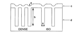
- the film-forming composition of the present invention has holes having an aspect ratio of 1 or more, for example, 1 to 10, or 2 to 5, as shown by the depth (b) / diameter (e) of holes as shown in FIG. It can be applied to a semiconductor substrate.
- the film-forming composition of the present invention can be used to fill such holes with a film without generating voids. Further, the film forming composition of the present invention can be applied to a semiconductor substrate (a substrate having a portion where holes are densely and sparsely present) having holes with an aspect ratio of 1 or more.
- the film formation composition of this invention can be used in order to form a flat film
- the film-forming composition of the present invention can also be used for a semiconductor substrate having holes with an aspect ratio smaller than 1 and a semiconductor substrate having steps.
- the film thickness of the film formed from the film-forming composition of the present invention is, for example, 20 to 2000 nm, 30 to 1000 nm, or 50 to 800 nm on the substrate surface.
- a photoresist can be formed on a film formed from the film-forming composition of the present invention. As a result, a laminated structure of the lower layer film and the photoresist is formed on the semiconductor substrate.
- the formation of the photoresist can be performed by a well-known method, that is, by applying a photoresist composition solution onto the lower layer film and heating.
- a photoresist composition solution onto the lower layer film and heating.
- membrane of this invention Both the negative type photoresist and the positive type photoresist which are used widely can be used.
- a positive photoresist comprising a novolak resin and 1,2-naphthoquinonediazide sulfonate
- a chemically amplified photoresist comprising a binder having a group that decomposes with an acid to increase the alkali dissolution rate and a photoacid generator
- Chemically amplified photoresist comprising a low molecular weight compound that decomposes with acid to increase the alkali dissolution rate of the photoresist, an alkali-soluble binder, and a photoacid generator
- chemically amplified photoresists composed of a low molecular weight compound that decomposes with acid and increases the alkali dissolution rate of the photoresist and a photoacid generator, such as the trade name APEX-E manufactured by Shipley, Sumitomo Chemical Co., Ltd. )
- a KrF excimer laser (wavelength 248 nm), an ArF excimer laser (wavelength 193 nm), an F2 excimer laser (wavelength 157 nm), or the like can be used.
- post-exposure bake can be performed as necessary.
- the post-exposure heating is appropriately selected from a heating temperature of 70 ° C. to 150 ° C. and a heating time of 0.3 to 10 minutes.
- development is performed with a developer.
- a developer for example, when a positive photoresist is used, the exposed portion of the photoresist is removed, and a photoresist pattern is formed.
- Developers include aqueous solutions of alkali metal hydroxides such as potassium hydroxide and sodium hydroxide, aqueous solutions of quaternary ammonium hydroxides such as tetramethylammonium hydroxide, tetraethylammonium hydroxide and choline, ethanolamine, propylamine, An alkaline aqueous solution such as an aqueous amine solution such as ethylenediamine can be mentioned as an example. Further, a surfactant or the like can be added to these developers.
- the development conditions are appropriately selected from a temperature of 5 to 50 ° C. and a time of 0.1 to 5 minutes.
- Removal of the lower layer film includes tetrafluoromethane (CF 4 ), perfluorocyclobutane (C 4 F 8 ), perfluoropropane (C 3 F 8 ), trifluoromethane, carbon monoxide, argon, oxygen, nitrogen, hexafluoride It can be performed by dry etching using a gas such as sulfur, difluoromethane, nitrogen trifluoride, and chlorine trifluoride.
- an antireflection film layer can be formed on the lower layer film before forming a photoresist.
- the antireflection film is not particularly limited, and an existing antireflection film can be used.
- an antireflection film is formed by a conventional method, for example, application onto a lower layer film by a spinner or a coater, and baking. Can be performed.
- the antireflection film composition examples include a light-absorbing compound, a resin and a solvent as a main component, a resin having a light-absorbing group linked by a chemical bond, a cross-linking agent and a solvent as a main component, and a light-absorbing compound. And those having a cross-linking agent and a solvent as main components and those having a light-absorbing polymer cross-linking agent and a solvent as main components.
- These anti-reflective coating compositions can also contain an acid component, an acid generator component, a rheology modifier, and the like, if necessary.
- Any light-absorbing compound can be used as long as it has a high absorption capability for light in the photosensitive characteristic wavelength region of the photosensitive component in the photoresist provided on the antireflection film.
- Examples include triazole compounds, azo compounds, naphthalene compounds, anthracene compounds, anthraquinone compounds, triazine compounds, and the like.
- Examples of the resin include polyester, polyimide, polystyrene, novolac resin, polyacetal resin, and acrylic resin.
- Examples of the resin having a light-absorbing group linked by a chemical bond include resins having a light-absorbing aromatic ring structure such as an anthracene ring, naphthalene ring, benzene ring, quinoline ring, quinoxaline ring, and thiazole ring.
- the underlayer film formed from the film-forming composition of the present invention may also absorb light depending on the wavelength of light used in the lithography process. In such a case, it can function as a layer having an effect of preventing reflected light from the substrate, that is, an antireflection film.
- the film of the present invention is a layer for preventing the interaction between the substrate and the photoresist, the material used for the photoresist, or the substance generated upon exposure to the photoresist to prevent the adverse effect on the semiconductor substrate. It can also be used as a layer, a layer for preventing diffusion of a substance generated from a semiconductor substrate upon heating and baking into an upper layer photoresist, and the like.
- Example 1 3.47 g of a photopolymerizable trehalose compound derivative represented by the above formula (1-3) to 13.57 g of cyclohexanone and 9.05 g of propylene glycol monomethyl ether acetate (manufactured by Gunei Chemical Industry Co., Ltd., trade name GS-TG001) , Photopolymerization initiator: 1-hydroxy-cyclohexyl-phenyl-ketone (Ciba Specialty Chemicals, trade name IRGACURE184) 0.35 g, and bis (2,4,6-trimethylbenzoyl) -phenylphosphine oxide ( Ciba Specialty Chemicals Co., Ltd., trade name IRGACURE 819) 0.17 g was added to give a 15% by mass solution. And it filtered using the polyethylene micro filter with the hole diameter of 0.2 micrometer, and prepared the solution of the lower layer film formation composition.
- a photopolymerizable trehalose compound derivative represented by the above formula (1-3
- Example 2 13.81 g of cyclohexanone, 9.21 g of propylene glycol monomethyl ether acetate, 3.53 g of a photopolymerizable butyl glucoside compound derivative represented by the above formula (1-4) (trade name GS-BG001, manufactured by Gunei Chemical Industry Co., Ltd.) ), Photopolymerization initiator: 1-hydroxy-cyclohexyl-phenyl-ketone (manufactured by Ciba Specialty Chemicals Co., Ltd., trade name IRGACURE184) 0.35 g, and bis (2,4,6-trimethylbenzoyl) -phenylphosphine oxide 0.18 g (trade name IRGACURE 819, manufactured by Ciba Specialty Chemicals Co., Ltd.) was added to make a 15% by mass solution. And it filtered using the polyethylene micro filter with the hole diameter of 0.2 micrometer, and prepared the solution of the lower layer film formation composition.
- Example 3 12.63 g of cyclohexanone, 8.42 g of propylene glycol monomethyl ether acetate, 3.23 g of a photopolymerizable methyl glucose ethylene oxide compound derivative represented by the above formula (1-5) (manufactured by Gunei Chemical Industry Co., Ltd., trade name GS) -EoG001), photopolymerization initiator: 1-hydroxy-cyclohexyl-phenyl-ketone (manufactured by Ciba Specialty Chemicals, trade name IRGACURE184) 0.32 g, and bis (2,4,6-trimethylbenzoyl) -phenylphos 0.16 g of fin oxide (manufactured by Ciba Specialty Chemicals Co., Ltd., trade name: IRGACURE 819) was added to make a 15% by mass solution. And it filtered using the polyethylene micro filter with the hole diameter of 0.2 micrometer, and prepared the solution of the lower layer film formation composition.
- Example 4 A photopolymerizable methylglucose ethylene oxide compound derivative represented by the above formula (1-6) 3.21 g (produced by Gunei Chemical Industry Co., Ltd., trade name GS) to 12.54 g of cyclohexanone and 8.36 g of propylene glycol monomethyl ether acetate -EoG002), photopolymerization initiator: 1-hydroxy-cyclohexyl-phenyl-ketone (manufactured by Ciba Specialty Chemicals, trade name IRGACURE184) 0.32 g, and bis (2,4,6-trimethylbenzoyl) -phenylphos 0.16 g of fin oxide (manufactured by Ciba Specialty Chemicals Co., Ltd., trade name: IRGACURE 819) was added to make a 15% by mass solution. And it filtered using the polyethylene micro filter with the hole diameter of 0.2 micrometer, and prepared the solution of the lower layer film formation composition.
- Example 5 25.09 g of cyclohexanone, 16.72 g of propylene glycol monomethyl ether acetate, 3.21 g of photopolymerizable methyl glucose ethylene oxide compound derivative represented by the above formula (1-6) (manufactured by Gunei Chemical Industry Co., Ltd., trade name GS) -EoG002), 3.21 g of photopolymerizable methylglucose compound derivative represented by the formula (1-2) (manufactured by Gunei Chemical Industry Co., Ltd., trade name GS-MG002) Photopolymerization initiator: 1-hydroxy- 0.64 g of cyclohexyl-phenyl-ketone (Ciba Specialty Chemicals Co., Ltd., trade name IRGACURE184) and bis (2,4,6-trimethylbenzoyl) -phenylphosphine oxide (Ciba Specialty Chemicals Co., Ltd., trade name) IRGACURE819) 0.32 g, and surface
- Example 6 1,2-epoxy-4- (2-oxiranyl) cyclosexane adduct of photopolymerization compound: 2,2-bis (hydroxymethyl) -1-butanol with 39.10 g of cyclohexanone and 26.07 g of propylene glycol monomethyl ether acetate And a mixture of 3,4-epoxycyclohexenylmethyl-3, '4'-epoxycyclohexenecarboxylate (Daicel Chemical Industries, Ltd., trade name liquid type EHPEL3150CE, a compound represented by the above formula (2-9))
- a mixture of compounds represented by the formula (2-1), a compound represented by the formula (2-9) has a molecular weight of 2234.) 10.00 g
- photopolymerization initiator triphenylsulfonium trifluoromethanesulfonate (Midori Chemical Co., Ltd., trade name TPS105) Add 1.00g and add 1 It was mass% solution.
- Example 7 Photopolymerizable 3,4-epoxycyclohexylmethyl-3,4-epoxycyclohexanecarboxylate represented by the above formula (2-1) in 39.10 g of cyclohexanone (produced by Daicel Chemical Industries, Ltd., trade name Celoxide 2021P) 10 0.005 g and photopolymerization initiator: 0.25 g of triphenylsulfonium trifluoromethanesulfonate (manufactured by Midori Chemical Co., Ltd., trade name TPS105) was added to make a 15 mass% solution. And it filtered using the polyethylene micro filter with the hole diameter of 0.2 micrometer, and prepared the solution of the lower layer film formation composition.
- cyclohexanone produced by Daicel Chemical Industries, Ltd., trade name Celoxide 2021P
- photopolymerization initiator 0.25 g of triphenylsulfonium trifluoromethanesulfonate (manufactured
- Example 8 An alicyclic epoxy resin compound having a photopolymerizable cyclohexene oxide skeleton represented by the above formula (2-4) on 39.10 g of cyclohexanone (manufactured by Daicel Chemical Industries, Ltd., trade name Celoxide 2081, n is 1) 00 g and photopolymerization initiator: 0.25 g of triphenylsulfonium trifluoromethanesulfonate (manufactured by Midori Chemical Co., Ltd., trade name TPS105) was added to make a 15% by mass solution. And it filtered using the polyethylene micro filter with the hole diameter of 0.2 micrometer, and prepared the solution of the lower layer film formation composition.
- Comparative Example 1 50 g of a solution containing 30 g of ethyl lactate and a copolymer of glycidyl methacrylate and methyl methacrylate obtained in Comparative Synthesis Example 1 (solid content concentration 20.0%), photopolymerization initiator: triphenylsulfonium trifluoromethanesulfonate (Midori Chemical ( Co., Ltd., trade name: TPS105) 0.50 g and surfactant (Dainippon Ink Chemical Co., Ltd., trade name: MegaFac R30) 0.05 g were added to make a 15% by mass solution. And it filtered using the polyethylene micro filter with the hole diameter of 0.2 micrometer, and prepared the solution of the lower layer film formation composition.
- photopolymerization initiator triphenylsulfonium trifluoromethanesulfonate
- surfactant Dainippon Ink Chemical Co., Ltd., trade name: MegaFac R30
- the dense pattern is a pattern in which the distance from the hole center to the adjacent hole center is one time the diameter of the hole.
- the depth of the hole is 1.0 ⁇ m, and the diameter of the hole is 0.30 or 1.0 ⁇ m.
- the coating film was irradiated for 2 minutes under an irradiation condition of 5.5 mW using an ultrahigh pressure mercury lamp (USHIO Electric Co., Ltd., model UIS-5011MIKY, output 500 W) (exposure amount 660 mJ / cm 2 ). .
- USHIO Electric Co., Ltd., model UIS-5011MIKY, output 500 W exposure amount 660 mJ / cm 2 .
- it was heated on a hot plate at 130 ° C. for 2 minutes to form a sacrificial film.
- the film thickness was 460 to 480 nm in an open area where there was no hole pattern nearby.
- the planarization rate by the sacrificial film was evaluated by observing the cross-sectional shape of the substrate using a scanning electron microscope (SEM).
- SEM scanning electron microscope
- the flattening rate was determined according to the following formula.
- the flattening rate when the holes on the substrate can be completely flattened is 100%.
- the results are shown in Table 1.
- Planarization rate ⁇ 1 ⁇ (depth of recess a in the lower layer film at the center of the hole a) / (depth of the hole b) ⁇ ⁇ 100
- no void (gap) was observed inside the hole, and it was observed that the inside of the hole was filled with a lower layer film.
- the film thickness difference (Bias) on the Iso (rough) and dense (dense) patterns of the sacrificial films of Examples 1 to 8 is small.
- the sacrificial films of Examples 1 to 8 are excellent in fluidity on a fine dense hole pattern where the film thickness is particularly difficult to be constant. This is because, even in the dense part where the number of holes per unit area on the hole substrate (hole density) is larger than that in the iso part, the solution of these many sacrificial film forming compositions flows smoothly, and a constant film thickness is obtained. As a result, it is considered that the film thickness difference between the Iso portion and the Dense portion is small and the flattening rate is large. Further, the sacrificial films of Examples 1 to 8 could be flattened regardless of the Iso portion and the Dense portion.
- the dry etching rate of the sacrificial film is higher than the dry etching rate of the photoresist.
- the photoresist formed on the sacrificial film is developed, and then the substrate base is exposed by dry etching.
- the sacrificial film's dry etching rate is higher than the photoresist's dry etching rate, so the sacrificial film is removed before the photoresist is scraped off, so the developed photoresist pattern can be accurately This is because it can be transferred to the substrate.
- a base permanent film such as an inorganic oxide film, an inorganic nitride film, and an inorganic oxynitride film.
- the sacrificial films obtained from the film forming compositions of Examples 1 to 8 have a wide range of dry etching selection ratios of 1.1 to 2.5 times. Therefore, in the manufacturing process of a light emitting diode, a solid-state imaging device, or a display device. It has been found that it has excellent compatibility with various underlying permanent films used and dry etching conditions.
- the film shrinkage rate of the sacrificial film is small. Excellent surface smoothness and gloss when coated on an uneven base permanent film. This is to obtain the effect of reducing the specific surface area for the property, light scattering prevention, and chemical solution protection.
- the sacrificial film obtained from the film-forming compositions of Examples 1 to 8 has excellent compatibility with various base permanent films used in the manufacturing process of semiconductors, light-emitting diodes, solid-state imaging devices, or display devices. all right.
- planarization film may be formed on a permanent film on a substrate, which is useful for producing these planarization films.
- FIG. 1 is a sectional view showing a state in which a lower layer film is formed on a semiconductor substrate having holes.
- a is the depth of the depression of the lower layer film at the center of the hole.
- b is the initial hole depth in the semiconductor substrate used.
- c is a lower layer film.
- d is a semiconductor substrate.
- e is the diameter of the hole.
Landscapes
- Physics & Mathematics (AREA)
- General Physics & Mathematics (AREA)
- Chemical & Material Sciences (AREA)
- Engineering & Computer Science (AREA)
- Spectroscopy & Molecular Physics (AREA)
- Materials Engineering (AREA)
- Architecture (AREA)
- Structural Engineering (AREA)
- Organic Chemistry (AREA)
- Wood Science & Technology (AREA)
- Life Sciences & Earth Sciences (AREA)
- Paints Or Removers (AREA)
- Epoxy Resins (AREA)
- Addition Polymer Or Copolymer, Post-Treatments, Or Chemical Modifications (AREA)
- Materials For Photolithography (AREA)
Abstract
La présente invention a trait à une composition filmogène permettant d'obtenir par photo-rayonnement un film de niveau utilisable dans un processus de nivelage d'une surface inégale. L'invention concerne également une composition filmogène permettant d'obtenir par photo-rayonnement un film de niveau utilisable dans un processus de nivelage d'une surface inégale, ladite composition contenant un matériau photopolymérisable et un initiateur de photopolymérisation. Ledit matériau photopolymérisable est un composé comportant au moins un groupe réactif pouvant subir une polymérisation cationique et ledit initiateur de photopolymérisation étant un initiateur de photopolymérisation cationique. En variante, ledit matériau photopolymérisable est un composé comportant au moins un groupe réactif pouvant subir une polymérisation radicalaire et ledit initiateur de photopolymérisation étant un initiateur de photopolymérisation radicalaire.
Priority Applications (1)
| Application Number | Priority Date | Filing Date | Title |
|---|---|---|---|
| JP2009554346A JP5545429B2 (ja) | 2008-02-20 | 2009-02-18 | 光硬化膜形成組成物及び光硬化膜形成方法 |
Applications Claiming Priority (2)
| Application Number | Priority Date | Filing Date | Title |
|---|---|---|---|
| JP2008039254 | 2008-02-20 | ||
| JP2008-039254 | 2008-02-20 |
Publications (1)
| Publication Number | Publication Date |
|---|---|
| WO2009104643A1 true WO2009104643A1 (fr) | 2009-08-27 |
Family
ID=40985521
Family Applications (1)
| Application Number | Title | Priority Date | Filing Date |
|---|---|---|---|
| PCT/JP2009/052798 Ceased WO2009104643A1 (fr) | 2008-02-20 | 2009-02-18 | Composition filmogène photodurcissable et procédé de formation d'un film photodurcissable |
Country Status (3)
| Country | Link |
|---|---|
| JP (1) | JP5545429B2 (fr) |
| TW (1) | TWI457711B (fr) |
| WO (1) | WO2009104643A1 (fr) |
Cited By (13)
| Publication number | Priority date | Publication date | Assignee | Title |
|---|---|---|---|---|
| JP2010260954A (ja) * | 2009-05-07 | 2010-11-18 | Toagosei Co Ltd | 2糖類の(メタ)アクリレートを含む硬化型組成物 |
| JP2011082236A (ja) * | 2009-10-05 | 2011-04-21 | Nissan Chem Ind Ltd | 半導体基板の平坦化方法 |
| WO2013115393A1 (fr) * | 2012-01-31 | 2013-08-08 | Canon Kabushiki Kaisha | Composition de résine négative photosensible, structure fine, procédé de production d'une structure fine et tête de sortie de liquide |
| JP2016075855A (ja) * | 2014-10-08 | 2016-05-12 | 大日本印刷株式会社 | 積層体の製造方法および積層体 |
| WO2019012716A1 (fr) * | 2017-07-13 | 2019-01-17 | 王子ホールディングス株式会社 | Composition pour la formation de films de sous-couche, procédé de formation de motifs et copolymère pour former un film de sous-couche utilisé pour la formation de motifs |
| WO2019163975A1 (fr) * | 2018-02-26 | 2019-08-29 | 王子ホールディングス株式会社 | Composition de formation de film de couche inférieure, procédé de formation de motif, copolymère et monomère pour composition de formation de film de couche inférieure |
| JP2020531872A (ja) * | 2017-08-29 | 2020-11-05 | 京東方科技集團股▲ふん▼有限公司Boe Technology Group Co.,Ltd. | 表示基板、表示装置及びその製造方法 |
| JP2021051312A (ja) * | 2019-07-02 | 2021-04-01 | 王子ホールディングス株式会社 | レジスト材料及びパターン形成方法 |
| CN113345992A (zh) * | 2020-03-03 | 2021-09-03 | 三星显示有限公司 | 发光装置 |
| WO2023033094A1 (fr) | 2021-09-02 | 2023-03-09 | 日産化学株式会社 | Composition de formation de film protecteur de bord de tranche pour la fabrication de semi-conducteurs |
| WO2023085414A1 (fr) | 2021-11-15 | 2023-05-19 | 日産化学株式会社 | Composition de résine photodurcissable aromatique et polycyclique à base d'hydrocarbure |
| WO2023162968A1 (fr) | 2022-02-22 | 2023-08-31 | 日産化学株式会社 | Composition de résine photodurcissable contenant un polymère auto-réticulant |
| WO2023171733A1 (fr) | 2022-03-10 | 2023-09-14 | 日産化学株式会社 | Composition de formation de film protecteur de bord de tranche pour la fabrication de semi-conducteurs |
Citations (4)
| Publication number | Priority date | Publication date | Assignee | Title |
|---|---|---|---|---|
| JPH1143501A (ja) * | 1997-07-29 | 1999-02-16 | Tokyo Ohka Kogyo Co Ltd | 変性セルロース化合物およびこれを含有する光重合性樹脂組成物 |
| WO2006115044A1 (fr) * | 2005-04-19 | 2006-11-02 | Nissan Chemical Industries, Ltd. | Composition de sous-couche de reserve permettant la formation d'une sous-couche de reserve durcie par photopolymerisation |
| JP2007017950A (ja) * | 2005-06-07 | 2007-01-25 | Shin Etsu Chem Co Ltd | レジスト下層膜材料並びにそれを用いたパターン形成方法 |
| WO2007066597A1 (fr) * | 2005-12-06 | 2007-06-14 | Nissan Chemical Industries, Ltd. | Composition de formation de film de couche sous-jacente de réserve contenant du silicium pour la formation de film de couche sous-jacente de réserve cuite par photo-réticulation |
Family Cites Families (3)
| Publication number | Priority date | Publication date | Assignee | Title |
|---|---|---|---|---|
| JPH11242111A (ja) * | 1998-02-26 | 1999-09-07 | Asahi Glass Co Ltd | カラーフィルタ保護膜用組成物、カラーフィルタ付き基板、その製法及び液晶表示素子 |
| JP2000344866A (ja) * | 1999-06-07 | 2000-12-12 | Jsr Corp | 平坦化膜用硬化性組成物および平坦化膜 |
| US6716767B2 (en) * | 2001-10-31 | 2004-04-06 | Brewer Science, Inc. | Contact planarization materials that generate no volatile byproducts or residue during curing |
-
2009
- 2009-02-18 WO PCT/JP2009/052798 patent/WO2009104643A1/fr not_active Ceased
- 2009-02-18 JP JP2009554346A patent/JP5545429B2/ja active Active
- 2009-02-20 TW TW098105474A patent/TWI457711B/zh active
Patent Citations (4)
| Publication number | Priority date | Publication date | Assignee | Title |
|---|---|---|---|---|
| JPH1143501A (ja) * | 1997-07-29 | 1999-02-16 | Tokyo Ohka Kogyo Co Ltd | 変性セルロース化合物およびこれを含有する光重合性樹脂組成物 |
| WO2006115044A1 (fr) * | 2005-04-19 | 2006-11-02 | Nissan Chemical Industries, Ltd. | Composition de sous-couche de reserve permettant la formation d'une sous-couche de reserve durcie par photopolymerisation |
| JP2007017950A (ja) * | 2005-06-07 | 2007-01-25 | Shin Etsu Chem Co Ltd | レジスト下層膜材料並びにそれを用いたパターン形成方法 |
| WO2007066597A1 (fr) * | 2005-12-06 | 2007-06-14 | Nissan Chemical Industries, Ltd. | Composition de formation de film de couche sous-jacente de réserve contenant du silicium pour la formation de film de couche sous-jacente de réserve cuite par photo-réticulation |
Cited By (16)
| Publication number | Priority date | Publication date | Assignee | Title |
|---|---|---|---|---|
| JP2010260954A (ja) * | 2009-05-07 | 2010-11-18 | Toagosei Co Ltd | 2糖類の(メタ)アクリレートを含む硬化型組成物 |
| JP2011082236A (ja) * | 2009-10-05 | 2011-04-21 | Nissan Chem Ind Ltd | 半導体基板の平坦化方法 |
| WO2013115393A1 (fr) * | 2012-01-31 | 2013-08-08 | Canon Kabushiki Kaisha | Composition de résine négative photosensible, structure fine, procédé de production d'une structure fine et tête de sortie de liquide |
| US9268222B2 (en) | 2012-01-31 | 2016-02-23 | Canon Kabushiki Kaisha | Photosensitive negative resin composition, fine structure, production process of fine structure and liquid ejection head |
| JP2016075855A (ja) * | 2014-10-08 | 2016-05-12 | 大日本印刷株式会社 | 積層体の製造方法および積層体 |
| WO2019012716A1 (fr) * | 2017-07-13 | 2019-01-17 | 王子ホールディングス株式会社 | Composition pour la formation de films de sous-couche, procédé de formation de motifs et copolymère pour former un film de sous-couche utilisé pour la formation de motifs |
| JP7079208B2 (ja) | 2017-08-29 | 2022-06-01 | 京東方科技集團股▲ふん▼有限公司 | 表示基板、表示装置及びその製造方法 |
| JP2020531872A (ja) * | 2017-08-29 | 2020-11-05 | 京東方科技集團股▲ふん▼有限公司Boe Technology Group Co.,Ltd. | 表示基板、表示装置及びその製造方法 |
| WO2019163975A1 (fr) * | 2018-02-26 | 2019-08-29 | 王子ホールディングス株式会社 | Composition de formation de film de couche inférieure, procédé de formation de motif, copolymère et monomère pour composition de formation de film de couche inférieure |
| JP2021051312A (ja) * | 2019-07-02 | 2021-04-01 | 王子ホールディングス株式会社 | レジスト材料及びパターン形成方法 |
| CN113345992A (zh) * | 2020-03-03 | 2021-09-03 | 三星显示有限公司 | 发光装置 |
| US12218291B2 (en) | 2020-03-03 | 2025-02-04 | Samsung Display Co., Ltd. | Light-emitting device |
| WO2023033094A1 (fr) | 2021-09-02 | 2023-03-09 | 日産化学株式会社 | Composition de formation de film protecteur de bord de tranche pour la fabrication de semi-conducteurs |
| WO2023085414A1 (fr) | 2021-11-15 | 2023-05-19 | 日産化学株式会社 | Composition de résine photodurcissable aromatique et polycyclique à base d'hydrocarbure |
| WO2023162968A1 (fr) | 2022-02-22 | 2023-08-31 | 日産化学株式会社 | Composition de résine photodurcissable contenant un polymère auto-réticulant |
| WO2023171733A1 (fr) | 2022-03-10 | 2023-09-14 | 日産化学株式会社 | Composition de formation de film protecteur de bord de tranche pour la fabrication de semi-conducteurs |
Also Published As
| Publication number | Publication date |
|---|---|
| TWI457711B (zh) | 2014-10-21 |
| JPWO2009104643A1 (ja) | 2011-06-23 |
| JP5545429B2 (ja) | 2014-07-09 |
| TW200944944A (en) | 2009-11-01 |
Similar Documents
| Publication | Publication Date | Title |
|---|---|---|
| JP5545429B2 (ja) | 光硬化膜形成組成物及び光硬化膜形成方法 | |
| JP5120577B2 (ja) | 光架橋硬化のレジスト下層膜を形成するためのレジスト下層膜形成組成物 | |
| TWI467338B (zh) | 含有具環狀胺基之聚矽氧的阻劑底層膜形成組成物 | |
| JP5083567B2 (ja) | 光架橋硬化によるレジスト下層膜を用いる半導体装置の製造方法 | |
| KR102044968B1 (ko) | 첨가제를 포함하는 규소함유 euv레지스트 하층막 형성 조성물 | |
| JP5440755B6 (ja) | 芳香族縮合環を含有する樹脂を含むリソグラフィー用レジスト下層膜形成組成物 | |
| TWI713461B (zh) | 具有鹵化磺醯基烷基之含有矽之光阻下層膜形成組成物 | |
| KR102382731B1 (ko) | 막밀도가 향상된 레지스트 하층막을 형성하기 위한 조성물 | |
| JP5660330B2 (ja) | 脂肪族環と芳香族環を含有する樹脂を含むリソグラフィー用レジスト下層膜形成組成物 | |
| WO2013047516A1 (fr) | Résine novolaque à base de diarylamine | |
| JP7626980B2 (ja) | 硬化性官能基を有する化合物を含む段差基板被覆組成物 | |
| JPWO2008069047A6 (ja) | 芳香族縮合環を含有する樹脂を含むリソグラフィー用レジスト下層膜形成組成物 | |
| WO2017094780A1 (fr) | Composition de formation d'un film de sous-couche de réserve contenant une résine novolaque indolocarbazole | |
| JPWO2018190380A1 (ja) | 炭素原子間の不飽和結合によるプラズマ硬化性化合物を含む段差基板被覆膜形成組成物 | |
| KR20150095693A (ko) | 카르보닐기함유 폴리하이드록시 방향환 노볼락수지를 포함하는 레지스트 하층막 형성조성물 | |
| JP2013137334A (ja) | ポリイミド構造を含有する樹脂を含むリソグラフィー用レジスト下層膜形成組成物 | |
| TWI583724B (zh) | 具有碸結構及胺結構之含有矽之阻劑底層膜形成組成物 | |
| KR20190131543A (ko) | 광가교기를 갖는 폴리에테르수지를 포함하는 단차기판 피복조성물 | |
| KR102632214B1 (ko) | 레지스트 하층막 형성 조성물 | |
| TW202302688A (zh) | 具有亞苄基氰乙酸酯基之阻劑下層膜形成組成物 | |
| TW202340308A (zh) | 具有羥基桂皮酸衍生物的阻劑下層膜形成用組成物 | |
| TW202336070A (zh) | 含有烷氧基之阻劑下層膜形成用組成物 |
Legal Events
| Date | Code | Title | Description |
|---|---|---|---|
| 121 | Ep: the epo has been informed by wipo that ep was designated in this application |
Ref document number: 09711864 Country of ref document: EP Kind code of ref document: A1 |
|
| ENP | Entry into the national phase |
Ref document number: 2009554346 Country of ref document: JP Kind code of ref document: A |
|
| NENP | Non-entry into the national phase |
Ref country code: DE |
|
| 122 | Ep: pct application non-entry in european phase |
Ref document number: 09711864 Country of ref document: EP Kind code of ref document: A1 |