WO2009107954A2 - 그래픽 가속기 및 그래픽 가속 방법 - Google Patents
그래픽 가속기 및 그래픽 가속 방법 Download PDFInfo
- Publication number
- WO2009107954A2 WO2009107954A2 PCT/KR2009/000850 KR2009000850W WO2009107954A2 WO 2009107954 A2 WO2009107954 A2 WO 2009107954A2 KR 2009000850 W KR2009000850 W KR 2009000850W WO 2009107954 A2 WO2009107954 A2 WO 2009107954A2
- Authority
- WO
- WIPO (PCT)
- Prior art keywords
- memory
- processor
- write command
- frame memory
- display device
- Prior art date
- Legal status (The legal status is an assumption and is not a legal conclusion. Google has not performed a legal analysis and makes no representation as to the accuracy of the status listed.)
- Ceased
Links
Images


Classifications
-
- G—PHYSICS
- G06—COMPUTING OR CALCULATING; COUNTING
- G06T—IMAGE DATA PROCESSING OR GENERATION, IN GENERAL
- G06T1/00—General purpose image data processing
- G06T1/20—Processor architectures; Processor configuration, e.g. pipelining
-
- G—PHYSICS
- G06—COMPUTING OR CALCULATING; COUNTING
- G06F—ELECTRIC DIGITAL DATA PROCESSING
- G06F1/00—Details not covered by groups G06F3/00 - G06F13/00 and G06F21/00
-
- G—PHYSICS
- G09—EDUCATION; CRYPTOGRAPHY; DISPLAY; ADVERTISING; SEALS
- G09G—ARRANGEMENTS OR CIRCUITS FOR CONTROL OF INDICATING DEVICES USING STATIC MEANS TO PRESENT VARIABLE INFORMATION
- G09G5/00—Control arrangements or circuits for visual indicators common to cathode-ray tube indicators and other visual indicators
- G09G5/36—Control arrangements or circuits for visual indicators common to cathode-ray tube indicators and other visual indicators characterised by the display of a graphic pattern, e.g. using an all-points-addressable [APA] memory
- G09G5/39—Control of the bit-mapped memory
- G09G5/395—Arrangements specially adapted for transferring the contents of the bit-mapped memory to the screen
-
- G—PHYSICS
- G09—EDUCATION; CRYPTOGRAPHY; DISPLAY; ADVERTISING; SEALS
- G09G—ARRANGEMENTS OR CIRCUITS FOR CONTROL OF INDICATING DEVICES USING STATIC MEANS TO PRESENT VARIABLE INFORMATION
- G09G2360/00—Aspects of the architecture of display systems
- G09G2360/08—Power processing, i.e. workload management for processors involved in display operations, such as CPUs or GPUs
Definitions
- the present invention relates to a graphics accelerator, and more particularly, to a graphics accelerator including a frame memory and having an interface such as a memory of a processor.
- the multimedia processor transmits data to an externally connected display device so that the user can visually check the contents.
- data to be displayed eg, an object, video data, a graphical user interface (GUI), etc.
- the display is implemented by reading and outputting recorded data by performing a direct memory access (DMA) operation or the like connected to the multimedia processor.
- the processor may be provided in a mobile device (mobile communication terminal, smartphone, etc.), and the display device may be an LCD, a TV, a projector, a monitor, or the like.
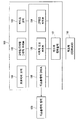
- FIG. 1 is a block diagram illustrating a processor connected to a display device and sharing a memory
- FIG. 2 is a block diagram illustrating a processor having a separate frame memory therein.
- the processor 100 includes a processor core 101, a 2D / 3D graphics processor 102, a video codec 103, a JPEG processor 104, an image signal processor 105, a display DMA 106, and the like.
- the memory 110 is shared and accessed through the memory controller 107.
- the processor core 101 controls each component of the processor 100, controls communication with an external device (eg, the display device 120, etc.), and performs basic functions of the processor 100. .
- the 2D / 3D graphic processing unit 102 performs a function related to a 2D graphic or a 3D graphic having values of points (vectors), lines, and colors using values of plane coordinates and colors.
- the video codec 103 performs encoding and / or decoding of multimedia data using a predetermined encoding scheme.
- the JPEG processing unit 104 compresses still images such as photographs according to a JPEG compression technique.
- the image signal processing unit 105 processes the image signal input from an image sensor or the like so as to be utilized by another processing unit.
- the display DMA 106 transmits the data stored in the predetermined area of the memory 110 to the display device 120 to be displayed by DMA transfer.
- a separate area in which data to be displayed on the display device 120 is stored is divided, which is called a frame memory area.
- the display DMA 330 continuously outputs the data in the frame memory area to the display device 120 connected to the outside.
- the frame memory area of the memory 110 should be output periodically according to the refresh rate. More refresh rates may be required for TVs or display devices with larger screen sizes.
- Periodically outputting the frame memory area according to the refresh rate affects the computing power of the processor core 101.
- a bottleneck occurs when the processor core 101 inputs / outputs data to the memory 110, and the computing power is reduced. It will weaken. That is, the memory bandwidth is weakened due to the external display device 120.
- the memory bandwidth refers to the frequency or bandwidth of accessing (reading or writing) data to the memory at a unit time, and the unit is also expressed as a byte value (bytes / sec) per second. That is, it shows the amount of data that can be accessed within a predetermined time.
- Each processor of the processor 100 can access a data rate, i.e., a memory bandwidth, that is accessible to a shared memory 110, which is always less than the maximum data rate that a single processor can access, i.e., the maximum memory bandwidth. You can only use it. Therefore, the memory bandwidth that can be shared and used by each processing unit, that is, the amount of data that can be accessed within a unit time, may increase as the number of processing units sharing the memory 110 decreases.
- the frame memory 108 is separated from the memory 110 and is provided in the processor 100 as a separate memory space in FIG. 2.
- the screen size that can be displayed is limited according to the size of the frame memory 108. Therefore, if the user wants to display on a wider screen, the frame memory needs to be made larger, so that a chip corresponding to the processor 100 must be manufactured separately.
- the present invention provides a graphics accelerator and a graphics acceleration method in which data corresponding to the frame memory is written to a graphics accelerator provided outside the processor so that the memory bandwidth of the processor is not reduced even by a continuous read operation by a DMA transfer of a display device. To provide.
- the present invention provides a graphics accelerator and a graphics acceleration method that can easily improve the configuration of the system because it is possible to change the interface with the display device from the outside with minimal changes without changing the processor itself.
- the present invention provides a graphic accelerator and a graphic acceleration method capable of improving the refresh rate and realizing a larger display resolution.
- a graphics accelerator connected between a processor and a display device.
- a graphics accelerator includes a frame memory; An accelerator controller having an input interface identical to that of the memory of the processor and writing data to be transmitted from the processor to the display device in the frame memory; And a display DMA for transferring data recorded in the frame memory to the display device.
- the accelerator controller may input and output the data from the processor through an SDRAM interface.
- the accelerator controller may analyze a write command of the processor to the memory, and copy data corresponding to the write command to the frame memory when the write command is a write command to a predetermined area in the memory.
- the data may be recorded in the frame memory by a memory map access method located on an extended memory map of the memory of the processor.
- the accelerator controller may receive a chip select signal for selecting a memory of the processor.
- the predetermined area may be a frame memory area of the memory.
- the accelerator controller compares first position information of a frame memory area of the memory previously input with second position information of the memory corresponding to the analyzed write command, so that the write command is applied to the frame memory area of the memory. It can be determined whether it is a write command.
- the apparatus may further include at least one of a camera signal processor and a graphic signal processor connected to the frame memory to perform an update.
- the display DMA may transmit the data to the display device according to a refresh rate or a request of the display device.
- a graphics acceleration method of a graphics accelerator connected between a processor and a display device and a recording medium on which a program for performing the graphics acceleration method is recorded.
- Graphic acceleration method the step of receiving a write command from the processor; And writing data to be transmitted from the processor to the display apparatus in a frame memory when the write command is input.
- the method may further include transmitting direct memory access (DMA) data recorded in the frame memory to the display apparatus according to a refresh rate of the display apparatus or a request.
- DMA direct memory access
- a graphic acceleration method comprising: determining whether a write command to a memory of the processor is input; Determining whether the write command is a write command to a frame memory area in the memory when the write command is input; And if the write command is a write command to the frame memory area, copying data corresponding to the write command to the frame memory.
- the method may further include transmitting direct memory access (DMA) data recorded in the frame memory to the display apparatus according to a refresh rate of the display apparatus or a request.
- DMA direct memory access
- the determining whether the write command is input may be determined by receiving a chip select signal for selecting a memory of the processor.
- determining whether the write command is a write command to a frame memory area in the memory corresponds to first position information of a frame memory area of the memory input in advance and the analyzed write command.
- the second position information of the memory may be compared to determine whether the write command is a write command to a frame memory area of the memory.
- 1 is a configuration block diagram of a processor connected to a display device and sharing a memory
- FIG. 2 is a block diagram illustrating a processor having a separate frame memory therein.
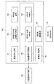
- FIG. 3 is a block diagram illustrating a graphics accelerator connected between a processor and a display device according to an embodiment of the present invention.
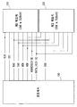
- FIG. 4 is a diagram illustrating a signal connection relationship between a first memory and a second memory using a general memory map connection method
- FIG. 5 is a diagram illustrating a signal connection relationship between a graphic accelerator and a memory and a processor having the same memory interface according to an embodiment of the present invention.
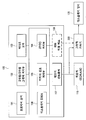
- FIG. 6 is a diagram illustrating a connection relationship between a processor, a graphic accelerator, and a display device according to the present invention.
- FIG. 7 is a flowchart of a graphic acceleration method of a graphic accelerator according to an embodiment of the present invention.
- FIG. 8 is a flowchart of a graphic acceleration method of a graphic accelerator according to another embodiment of the present invention.
- FIG. 9 is a block diagram illustrating a graphic accelerator connected between a processor and a display device according to another embodiment of the present invention.
- first and second may be used to describe various components, but the components should not be limited by the terms. The terms are used only for the purpose of distinguishing one component from another.
- the first component may be referred to as the second component, and similarly, the second component may also be referred to as the first component.
- FIG. 3 is a block diagram illustrating a graphic accelerator connected between a processor and a display device according to an embodiment of the present invention.
- 4 is a diagram illustrating a signal connection relationship between a first memory and a second memory by a general memory map connection method
- FIG. 5 is a signal of a graphic accelerator, a memory, and a processor having the same memory interface according to an embodiment of the present invention. It is a figure which shows the connection relationship.
- 6 is a diagram illustrating a connection relationship between a processor, a graphic accelerator, and a display device according to the present invention.
- the graphics accelerator 300 is connected to the processor 100 and the display device 120 between the processor 100 and the display device 120.
- the processor 100 is a multimedia processor including a graphics processor, a video codec, a JPEG processor, an image signal processor, and the like, and may be a processor provided in a mobile device (mobile communication terminal, smart phone, etc.).
- the display device 120 refers to a device capable of implementing a display by receiving data such as an LCD, a TV, a projector, a monitor, and the like.
- the graphics accelerator 300 includes an accelerator controller 310, a frame memory 320, and a display DMA 330.
- the processor 100 does not write data to be transmitted to the display apparatus 120 to the graphic accelerator 300 directly, instead of writing the data to the memory 110 shared by each processing unit as before.
- the accelerator controller 310 has the same interface as the memory 110 on the input side.
- the memory 110 of the processor 100 may be a single data rate (SDR) or a double data rate (DDR) SDRAM. Accordingly, the accelerator controller 310 may input / output data from the processor 100 through an SDRAM interface such as SDR or DDR.
- the accelerator controller 310 receives a write command directly from the processor 100 and writes data corresponding to the write command in the frame memory 320.
- the data recorded in the frame memory 320 is the content that the processor 100 wants to display through the display device 120, that is, a predetermined screen (still image or video, etc.) or updated content of a screen already displayed. Is related to.
- the display DMA 120 transmits the data recorded in the frame memory 320 to the display device 120.
- the display DMA 120 may transmit data recorded in the frame memory 320 to the display device 120 according to a refresh rate or a request of the display device 120.
- the read operation to the display device 120 is performed through the frame memory 320 of the graphic accelerator 300. This is performed regardless of the memory 110 shared by the processor 100, so that the memory bandwidth of the memory 110 may not be reduced.
- graphics accelerator 300 includes accelerator controller 310, frame memory 320, and display DMA 330. It is assumed that the processor 100 includes a memory 110 shared by respective processing units, and a predetermined area of the memory 110 is allocated as a frame memory area for display. Accordingly, the processor 100 accesses the frame memory area of the memory 110 to record data when displaying a predetermined screen (still image or moving image, etc.) or updating an already displayed screen. Update.
- the accelerator controller 310 has the same interface as the memory 110 connected to the processor 100 on the input side.
- the accelerator controller 310 may recognize this.
- the write operation may also include an update.
- the accelerator controller 310 may be connected to the processor 100 through a memory bus or a separate external serial bus. When connected through a memory bus, some of the memory buses connected between the processor 100 and the memory 110 may be shared.
- the accelerator controller 310 After the accelerator controller 310 recognizes a write command from the processor 100 to the memory 110, the accelerator controller 310 determines whether the corresponding write command is a write command to an area allocated to the frame memory area of the memory 110. In the case of a write command to the frame memory area, the accelerator controller 310 copies data corresponding to the write command stored in the frame memory area of the memory 110 to the frame memory 320.
- the read operation to the display device 120 is performed only in the frame memory 320 of the graphic accelerator 300, not in the memory 110. Through this, the memory bandwidth of the memory 110 shared by the processor 100 may not be reduced.
- the accelerator controller 310 has an SDRAM interface such as SDR or DDR on the input side, which is preferably the same as the memory 110 of the processor 100.
- the memory map access method is a method of distinguishing data access by a chip select signal while two or more memories write a control signal and a data signal at the same time, and is mainly used to increase the capacity of the memory.
- the control signal includes a readable signal (REN), a writable signal (WEN), a row address strobe (RAS), a column address strobe (CAS), an address signal (ADDRESS), and the data signal is a data input / output line (DATA_IO). Is passed through).
- the chip select signals CS1 and CS2 are a kind of control signal, but are used for selecting a specific memory.
- the first chip select signal CS1 selects the first memory 210 and the second chip select signal CS2 selects the second memory 220.
- the first chip select signal and the second chip select signal are not simultaneously accessed by the general attributes of the memory controller included in the processor 100.
- One memory is selected only when the memory address is mapped to another memory address. For example, from 0 to 1M, only the first memory 210 is activated by the first chip select signal, and the second memory 220 is operated as if it is not disabled.
- the memory 110 shared by the processor 100 corresponds to the first memory 210
- the graphics accelerator 300 corresponds to the second memory 220.
- the graphics accelerator 300 detects that a write operation is performed at a corresponding address when a predetermined area of the memory 110 is written (including an update) to the frame memory area, and the same contents are stored in the internal frame memory 320. Operate to be recorded.
- the first chip select signal CS1 should be additionally connected.
- the graphics accelerator 300 detects that the write operation of the processor 100 to the memory 110 is performed through the memory bus. This operation is performed in the accelerator controller 310.
- the accelerator controller 310 includes a separate storage unit, and first location information about an address and a size of a frame memory area located in the memory 110 is input in advance.
- the accelerator controller 310 detects that the write operation is performed to the memory 110, the accelerator controller 310 obtains second position information of the memory 110 related to the current write operation through the memory bus. Thus, the accelerator controller 310 compares the first position information with the second position information. That is, information about the address of the memory 110 associated with performing the write operation and the address and size of the frame memory area located in the memory 110 that are input in advance are compared. When the write operation is currently performed in the frame memory area, the copy operation of the same data is executed by the frame memory 320 inside the graphic accelerator 300.
- the accelerator controller 310 performs a current write operation via an external serial bus 109 (eg, a serial peripheral interface (SPI), etc.) of the processor 100. Information about the address of the memory 110 being used may be received.
- an external serial bus 109 eg, a serial peripheral interface (SPI), etc.
- the display DMA 330 of the graphics accelerator 300 DMA transfers the data recorded in the frame memory 320 to the display device 120 periodically or by request.
- the display device 120 does not access the memory 110 of the processor 100, but accesses only the frame memory 320 of the graphic accelerator 300 to perform a read operation.
- the display DMA 330 of the graphics accelerator 300 performs the above-described operation, the display DMA 330 of the processor may be suspended. In this case, since only the function of the display DMA 330 provided in the existing processor 100 needs to be stopped, there is an advantage of minimizing a software change in the processor 100 for applying the present invention.
- the accelerator controller 310 has the same interface as the memory 110 of the processor 100 and is connected to the processor 100.
- the accelerator controller 310 may also receive a write command from the processor 100 (step 710).
- the write command also includes a command for updating data recorded in the frame memory 320.
- the accelerator controller 310 stores data input from the processor 100 in the frame memory 320 according to the input write command (step 720).
- the data stored in the frame memory 320 may be DMA transferred to the display device 120 by a periodic request or an arbitrary request according to the refresh rate of the display device 120 (step 730).
- FIG. 8 is a flowchart of a graphic acceleration method of a graphic accelerator according to another embodiment of the present invention.
- the accelerator controller 310 is connected to the memory controller 107 of the processor 100 through a memory bus.
- the first chip selection signal for selecting the memory 110 of the processor 100 is also input to the accelerator controller 310.
- the accelerator controller 310 determines whether a write operation to the memory 110 of the processor 100 is being performed according to whether the first chip selection signal is input (step 810). If the write operation is not being performed, step 810 is repeated until the first chip select signal is input.
- the accelerator controller 310 determines whether the area of the memory 110 associated with the write operation is a frame memory area associated with the display. It is determined whether or not (step 820). If a write operation is performed in an area other than the frame memory area, the process returns to step 810 not related to the present invention.
- Whether the area in which the write operation is being performed is the frame memory area may be determined based on the address and the size of the frame memory area previously input to the accelerator controller 310.
- the accelerator controller 310 may write data written to the memory 110 of the processor 100 through the memory bus to the frame memory (eg, the graphics accelerator 300). The same is also copied to 320 (step 830).
- the data copied to the frame memory 320 of the graphic accelerator 300 may be DMA-transferred to the display apparatus 120 according to the refresh rate of the display apparatus 120 or on request (step 840).
- the memory bandwidth utilization in the processor can be freed, and the display and frame memory are frequently updated. It can accommodate various requirements related to functions.
- LCDs mainly use a parallel bus, which is changing to a new serial interface such as a mobile industry processor interface (MIPI) or a mobile display digital interface (MDDI). to be.
- MIPI mobile industry processor interface
- MDDI mobile display digital interface
- MIPI mobile industry processor interface
- MDDI mobile display digital interface
- the refresh rate can be improved and a larger display resolution can be realized because the memory bandwidth is high by utilizing the frame memory of the graphic accelerator. If the refresh rate is high, it is possible to produce a display device with a more natural feeling because the screen does not feel interrupted even on a large screen.
- the graphic acceleration method of the graphic accelerator described above with reference to FIG. 7 or 8 may be created by a computer program. Codes and code segments constituting the program can be easily inferred by a computer programmer in the art.
- the program is stored in a computer readable media, and read and executed by a computer, thereby implementing a graphic acceleration method of a graphic accelerator.
- the information storage medium includes a magnetic recording medium, an optical recording medium, and a carrier wave medium.
- FIG. 9 is a block diagram illustrating a graphic accelerator connected between a processor and a display device according to another embodiment of the present invention.
- the functions of the accelerator controller 310, the frame memory 320, and the display DMA 330 are the same as those shown in FIG. 3, and thus a detailed description thereof will be omitted.
- the graphics accelerator 300 may further include a camera signal processor 340 and / or a graphic signal processor 350, which should frequently update the frame memory 320.
- the camera signal processor 340 and / or the 2D / 3D graphic signal processor 350 connected to the camera module may be provided in the graphic accelerator 300 separately from the processor 100 to frequently update the frame memory 320.
- the memory bandwidth of the processor 100 may not be affected.
- a graphic accelerator and a graphic acceleration method write data corresponding to a frame memory in a graphic accelerator provided outside the processor so that the memory bandwidth of the processor is not reduced even by a continuous read operation by a DMA transfer of a display device. It works.
- the configuration of the system can be easily improved since the interface with the display device can be changed externally with minimal changes without changing the processor itself.
- the present invention can improve the refresh rate and realize a larger display resolution.
Landscapes
- Engineering & Computer Science (AREA)
- Theoretical Computer Science (AREA)
- Physics & Mathematics (AREA)
- General Physics & Mathematics (AREA)
- Computer Hardware Design (AREA)
- General Engineering & Computer Science (AREA)
- Controls And Circuits For Display Device (AREA)
- Image Generation (AREA)
- Digital Computer Display Output (AREA)
Abstract
Description
Claims (16)
- 프로세서와 디스플레이 장치 사이에 연결되는 그래픽 가속기에 있어서,프레임 메모리;입력측에 상기 프로세서의 메모리와 동일한 인터페이스를 가지고, 상기 프로세서로부터 상기 디스플레이 장치로 전송하고자 하는 데이터를 상기 프레임 메모리에 기록하는 가속기 컨트롤러; 및상기 프레임 메모리에 기록된 데이터를 상기 디스플레이 장치로 DMA(Direct Memory Access) 전송하는 디스플레이 DMA를 포함하는 그래픽 가속기.
- 제1항에 있어서,상기 가속기 컨트롤러는 SDRAM 인터페이스를 통하여 상기 프로세서로부터 상기 데이터를 입출력하는 것을 특징으로 하는 그래픽 가속기.
- 제1항에 있어서,상기 가속기 컨트롤러는 상기 프로세서의 상기 메모리로의 쓰기 명령을 분석하고, 상기 쓰기 명령이 상기 메모리 내의 소정 영역에의 쓰기 명령인 경우 상기 쓰기 명령에 상응하는 데이터를 상기 프레임 메모리로 복사하는 것을 특징으로 하는 그래픽 가속기.
- 제3항에 있어서,상기 가속기 컨트롤러는 상기 프로세서의 메모리를 선택하는 칩 선택 신호를 함께 입력받는 것을 특징으로 하는 그래픽 가속기.
- 제3항에 있어서,상기 소정 영역은 상기 메모리 중 프레임 메모리 영역인 것을 특징으로 하는 그래픽 가속기.
- 제5항에 있어서,상기 가속기 컨트롤러는 미리 입력된 상기 메모리의 프레임 메모리 영역의 제1 위치 정보와, 상기 분석한 쓰기 명령에 상응하는 상기 메모리의 제2 위치 정보를 비교하여 상기 쓰기 명령이 상기 메모리의 프레임 메모리 영역에의 쓰기 명령인지 여부를 판단하는 것을 특징으로 하는 그래픽 가속기.
- 제3항에 있어서,상기 프레임 메모리는 상기 프로세서의 메모리의 연장된 메모리 맵 상에 위치하는 메모리 맵 접속 방식에 의해 상기 데이터가 기록되는 것을 특징으로 하는 그래픽 가속기.
- 제1항에 있어서,상기 프레임 메모리에 연결되어 업데이트(update)를 수행하는 카메라 신호처리부 및 그래픽 신호처리부 중 적어도 하나를 더 포함하는 것을 특징으로 하는 그래픽 가속기.
- 제1항에 있어서,상기 디스플레이 DMA는 상기 디스플레이 장치의 리프레시 레이트(refresh rate) 또는 요청에 따라 상기 데이터를 상기 디스플레이 장치로 전송하는 것을 특징으로 하는 그래픽 가속기.
- 프로세서와 디스플레이 장치 사이에 연결되는 그래픽 가속기의 그래픽 가속 방법에 있어서,상기 프로세서로부터 쓰기 명령을 입력받는 단계; 및상기 쓰기 명령이 입력되는 경우 상기 프로세서로부터 상기 디스플레이 장치로 전송하고자 하는 데이터를 프레임 메모리에 기록하는 단계를 포함하는 그래픽 가속 방법.
- 제10항에 있어서,상기 디스플레이 장치의 리프레시 레이트(refresh rate)에 따라 또는 요청에 따라 상기 프레임 메모리에 기록된 데이터를 상기 디스플레이 장치로 DMA(Direct Memory Access) 전송하는 단계를 더 포함하는 그래픽 가속기의 그래픽 가속 방법.
- 프로세서와 디스플레이 장치 사이에 연결되는 그래픽 가속기의 그래픽 가속 방법에 있어서,상기 프로세서의 메모리로의 쓰기 명령이 입력되는지 판단하는 단계;상기 쓰기 명령이 입력되는 경우 상기 쓰기 명령이 상기 메모리 내의 프레임 메모리 영역에의 쓰기 명령인지 판단하는 단계; 및상기 쓰기 명령이 상기 프레임 메모리 영역에의 쓰기 명령인 경우 상기 쓰기 명령에 상응하는 데이터를 상기 프레임 메모리로 복사하는 단계를 포함하는 그래픽 가속기의 그래픽 가속 방법.
- 제12항에 있어서,상기 디스플레이 장치의 리프레시 레이트(refresh rate)에 따라 또는 요청에 따라 상기 프레임 메모리에 기록된 데이터를 상기 디스플레이 장치로 DMA(Direct Memory Access) 전송하는 단계를 더 포함하는 그래픽 가속기의 그래픽 가속 방법.
- 제12항에 있어서,상기 쓰기 명령이 입력되는지 판단하는 단계는, 상기 프로세서의 메모리를 선택하는 칩 선택 신호를 함께 입력받음으로써 판단하는 것을 특징으로 하는 그래픽 가속기의 그래픽 가속 방법.
- 제12항에 있어서,상기 쓰기 명령이 입력되는 경우 상기 쓰기 명령이 상기 메모리 내의 프레임 메모리 영역에의 쓰기 명령인지 판단하는 단계는,미리 입력된 상기 메모리의 프레임 메모리 영역의 제1 위치 정보와, 상기 분석한 쓰기 명령에 상응하는 상기 메모리의 제2 위치 정보를 비교하여 상기 쓰기 명령이 상기 메모리의 프레임 메모리 영역에의 쓰기 명령인지 여부를 판단하는 것을 특징으로 하는 그래픽 가속기의 그래픽 가속 방법.
- 제10항 내지 제15항 중 어느 한 항에 기재된 그래픽 가속기의 그래픽 가속 방법을 수행하기 위하여 컴퓨터 장치에서 실행될 수 있는 명령어들의 프로그램이 기록되어 있으며, 상기 컴퓨터 장치에 의해 판독될 수 있는 프로그램이 기록된 기록매체.
Priority Applications (2)
| Application Number | Priority Date | Filing Date | Title |
|---|---|---|---|
| US12/919,307 US20110010472A1 (en) | 2008-02-27 | 2009-02-23 | Graphic accelerator and graphic accelerating method |
| GB1014376A GB2469607A (en) | 2008-02-27 | 2009-02-23 | Graphic accelerator and graphic accelerating method |
Applications Claiming Priority (2)
| Application Number | Priority Date | Filing Date | Title |
|---|---|---|---|
| KR10-2008-0017708 | 2008-02-27 | ||
| KR1020080017708A KR100941029B1 (ko) | 2008-02-27 | 2008-02-27 | 그래픽 가속기 및 그래픽 가속 방법 |
Publications (2)
| Publication Number | Publication Date |
|---|---|
| WO2009107954A2 true WO2009107954A2 (ko) | 2009-09-03 |
| WO2009107954A3 WO2009107954A3 (ko) | 2009-11-26 |
Family
ID=40024029
Family Applications (1)
| Application Number | Title | Priority Date | Filing Date |
|---|---|---|---|
| PCT/KR2009/000850 Ceased WO2009107954A2 (ko) | 2008-02-27 | 2009-02-23 | 그래픽 가속기 및 그래픽 가속 방법 |
Country Status (4)
| Country | Link |
|---|---|
| US (1) | US20110010472A1 (ko) |
| KR (1) | KR100941029B1 (ko) |
| GB (1) | GB2469607A (ko) |
| WO (1) | WO2009107954A2 (ko) |
Families Citing this family (7)
| Publication number | Priority date | Publication date | Assignee | Title |
|---|---|---|---|---|
| US10141314B2 (en) * | 2011-05-04 | 2018-11-27 | Micron Technology, Inc. | Memories and methods to provide configuration information to controllers |
| US10355001B2 (en) | 2012-02-15 | 2019-07-16 | Micron Technology, Inc. | Memories and methods to provide configuration information to controllers |
| KR101337950B1 (ko) * | 2012-02-24 | 2013-12-06 | 주식회사 휴비츠 | 그래픽 데이터 출력 장치 및 방법 |
| KR102301536B1 (ko) * | 2015-03-10 | 2021-09-14 | 삼성전자주식회사 | 고해상도 전자 현미경 이미지로부터 결정을 분석하는 방법 및 그 시스템 |
| JP6969295B2 (ja) * | 2017-10-31 | 2021-11-24 | 富士フイルムビジネスイノベーション株式会社 | 情報処理装置及び画像処理システム |
| CN108897706B (zh) * | 2018-05-10 | 2021-07-23 | 北京融芯微科技有限公司 | 一种加速器接口 |
| US20250005704A1 (en) * | 2023-06-28 | 2025-01-02 | Texas Instruments Incorporated | Methods and apparatus to animate a splash screen |
Family Cites Families (10)
| Publication number | Priority date | Publication date | Assignee | Title |
|---|---|---|---|---|
| JPH1069428A (ja) * | 1996-08-28 | 1998-03-10 | Nec Corp | ビデオ表示装置 |
| US6501480B1 (en) * | 1998-11-09 | 2002-12-31 | Broadcom Corporation | Graphics accelerator |
| JP2000293151A (ja) | 1999-04-07 | 2000-10-20 | Nec Corp | グラフィックス表示装置及びディスプレイリストによるグラフィックス表示方法 |
| JP2001195050A (ja) * | 1999-11-05 | 2001-07-19 | Mitsubishi Electric Corp | グラフィックアクセラレータ |
| US6903739B2 (en) * | 2001-02-20 | 2005-06-07 | Ati International Srl | Graphic display system having a frame buffer with first and second memory portions |
| US6999091B2 (en) * | 2001-12-28 | 2006-02-14 | Intel Corporation | Dual memory channel interleaving for graphics and video |
| US6931484B2 (en) * | 2002-04-25 | 2005-08-16 | Intel Corporation | Method and apparatus for handling memory refresh and maintenance operations |
| KR100510131B1 (ko) * | 2003-01-29 | 2005-08-26 | 삼성전자주식회사 | 픽셀 캐쉬 및 이를 이용한 3차원 그래픽 가속 장치 및 방법 |
| US20060007200A1 (en) * | 2004-07-08 | 2006-01-12 | David Young | Method and system for displaying a sequence of image frames |
| US7362325B2 (en) * | 2004-12-21 | 2008-04-22 | Qualcomm Incorporated | 2D/3D line rendering using 3D rasterization algorithms |
-
2008
- 2008-02-27 KR KR1020080017708A patent/KR100941029B1/ko not_active Expired - Fee Related
-
2009
- 2009-02-23 GB GB1014376A patent/GB2469607A/en not_active Withdrawn
- 2009-02-23 WO PCT/KR2009/000850 patent/WO2009107954A2/ko not_active Ceased
- 2009-02-23 US US12/919,307 patent/US20110010472A1/en not_active Abandoned
Also Published As
| Publication number | Publication date |
|---|---|
| KR100941029B1 (ko) | 2010-02-05 |
| GB2469607A (en) | 2010-10-20 |
| US20110010472A1 (en) | 2011-01-13 |
| WO2009107954A3 (ko) | 2009-11-26 |
| GB201014376D0 (en) | 2010-10-13 |
| KR20080083235A (ko) | 2008-09-17 |
Similar Documents
| Publication | Publication Date | Title |
|---|---|---|
| WO2009107954A2 (ko) | 그래픽 가속기 및 그래픽 가속 방법 | |
| US20140129738A1 (en) | Flexible Implementation of Serial Bus Support Over Display Interface | |
| KR100245821B1 (ko) | 비디오 인터페이스와 오버레이시스템 및 그의 프로세스 | |
| US6734862B1 (en) | Memory controller hub | |
| JPH0827705B2 (ja) | アダプタ | |
| US6006287A (en) | DMA transfer of an interleaved stream | |
| JPH0827773B2 (ja) | データ経路を使用可能にする方法、装置およびデータ処理システム | |
| WO2013105716A1 (ko) | 이미지 제공 시스템, 이를 위한 장치 및 이미지 제공 방법 | |
| KR100218265B1 (ko) | 우선 순위 요구 및 바이패스 버스 | |
| WO2020153616A2 (ko) | 캐스케이드 연결 구조의 호스트와 슬레이브 장치 | |
| US5752010A (en) | Dual-mode graphics controller with preemptive video access | |
| US5784592A (en) | Computer system which includes a local expansion bus and a dedicated real-time bus for increased multimedia performance | |
| US6189075B1 (en) | Circuit for the management of memories in a multiple-user environment with access request and priority | |
| WO2017122845A1 (ko) | 채널별 이종 동작을 위한 멀티채널 초고해상도 영상 획득/재생 시스템 및 방법 | |
| US20170220069A1 (en) | Docking apparatus and control method thereof | |
| JP2003177958A (ja) | 特殊メモリデバイス | |
| WO2024071652A1 (ko) | 전자 장치 및 그 제어 방법 | |
| JP3033747B1 (ja) | 多画面表示回路および多画面表示回路を搭載した携帯端末機器 | |
| KR100284420B1 (ko) | 디지털 비디오 캡쳐 보드 | |
| JP3204297B2 (ja) | Dma転送制御装置 | |
| WO2023096079A1 (ko) | 디스플레이 장치 및 제어 방법 | |
| WO2022203258A1 (ko) | 전자 장치 및 그 제어 방법 | |
| CN121788333A (zh) | 基于几何缓冲区的图像信号处理方法、处理设备、介质及产品 | |
| WO2024155074A1 (ko) | 전자 장치 및 전자 장치의 메모리 관리 방법 | |
| CN116527831A (zh) | 一种实现高速率和低功耗双向读写的数据传输系统以及信号发生器 |
Legal Events
| Date | Code | Title | Description |
|---|---|---|---|
| 121 | Ep: the epo has been informed by wipo that ep was designated in this application |
Ref document number: 09715146 Country of ref document: EP Kind code of ref document: A2 |
|
| ENP | Entry into the national phase |
Ref document number: 1014376 Country of ref document: GB Kind code of ref document: A Free format text: PCT FILING DATE = 20090223 |
|
| WWE | Wipo information: entry into national phase |
Ref document number: 1014376.6 Country of ref document: GB |
|
| WWE | Wipo information: entry into national phase |
Ref document number: 12919307 Country of ref document: US |
|
| NENP | Non-entry into the national phase |
Ref country code: DE |
|
| 32PN | Ep: public notification in the ep bulletin as address of the adressee cannot be established |
Free format text: NOTING OF LOSS OF RIGHTS PURSUANT TO RULE 112(1) EPC (EPO FORM 1205A DATED 04/11/10) |
|
| 122 | Ep: pct application non-entry in european phase |
Ref document number: 09715146 Country of ref document: EP Kind code of ref document: A2 |