WO2009118832A1 - Dispositif de saisie d'images d'un rayonnement - Google Patents
Dispositif de saisie d'images d'un rayonnement Download PDFInfo
- Publication number
- WO2009118832A1 WO2009118832A1 PCT/JP2008/055595 JP2008055595W WO2009118832A1 WO 2009118832 A1 WO2009118832 A1 WO 2009118832A1 JP 2008055595 W JP2008055595 W JP 2008055595W WO 2009118832 A1 WO2009118832 A1 WO 2009118832A1
- Authority
- WO
- WIPO (PCT)
- Prior art keywords
- voltage
- temperature
- control means
- conversion layer
- peltier element
- Prior art date
- Legal status (The legal status is an assumption and is not a legal conclusion. Google has not performed a legal analysis and makes no representation as to the accuracy of the status listed.)
- Ceased
Links
Images


Classifications
-
- G—PHYSICS
- G01—MEASURING; TESTING
- G01T—MEASUREMENT OF NUCLEAR OR X-RADIATION
- G01T1/00—Measuring X-radiation, gamma radiation, corpuscular radiation, or cosmic radiation
- G01T1/16—Measuring radiation intensity
- G01T1/24—Measuring radiation intensity with semiconductor detectors
- G01T1/244—Auxiliary details, e.g. casings, cooling, damping or insulation against damage by, e.g. heat, pressure or the like
Definitions
- the present invention relates to a radiation imaging apparatus that detects radiation and outputs an image signal, and particularly relates to a radiation imaging apparatus having a configuration for performing temperature control using a Peltier element.
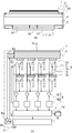
- a conventional radiation imaging apparatus has a configuration as shown in FIG.
- the radiation incident on the radiation imaging apparatus is converted into electric charges by the X-ray conversion layer 2 formed of a semiconductor thick film such as amorphous selenium.
- the charge is opposite to that of the bias application electrode 1 due to a bias voltage VA applied between the bias application electrode 1 provided on the radiation incident side of the X-ray conversion layer 2 and the ground side of the capacitor Ca described later.
- Reading is performed by the TFT substrate 3 provided on the side.
- the TFT substrate has a pixel electrode 31 provided in a matrix for collecting charges, a capacitor Ca connected to the pixel electrode 31, and a thin film transistor element Tr having a source connected to the capacitor Ca. .
- the TFT substrate 3 includes a gate line G commonly connected to the gates of the thin film transistor elements Tr belonging to the same row and a data line D commonly connected to the drains of the thin film transistor elements Tr belonging to the same column. Have only.
- the charge generated in the pixel DU is accumulated in the capacitor Ca through the corresponding pixel electrode 31.
- the accumulated charge is read out to the data line D of the column to which the pixel DU belongs by turning on the thin film transistor element Tr when the potential of the gate line G of the column to which the pixel DU belongs becomes ON potential.
- the potential of the gate line G in each row is controlled by the gate drive circuit 5.
- the TFT substrate 3 is held on one surface of a base substrate 4 such as aluminum, and an amplifier / A / D conversion circuit 6 is disposed on the other surface of the base substrate.
- the data line D of the TFT substrate 3 and the charge amplifier 61 of the amplifier / A / D conversion circuit 6 are connected by a flexible substrate 63.
- the electric charge read out to the data line D is converted into a voltage by the charge amplifier 61, converted into a pixel value by the A / D conversion circuit 62 connected to the charge amplifier 61, and then stored in the memory unit 71.
- the pixel values stored in the memory unit 71 are transferred to the image processing device 8. These series of operations are controlled by the controller 7 (see, for example, Patent Document 1).
- the thermal expansion coefficient with the substrate (active matrix substrate) on which the X-ray conversion layer 2 is deteriorated due to a temperature change or the thin film transistor element holding the X-ray conversion layer 2 is formed Due to these differences, problems such as film peeling and cracking have occurred.
- a thermistor 91 that detects the temperature of the X-ray conversion layer 2
- a Peltier element 92 that changes the temperature of the X-ray conversion layer 2
- a temperature that controls the voltage applied to the Peltier element 92 based on the detected temperature has been proposed (see, for example, Patent Document 2).
- An object of the present invention is to provide a high-quality image with less noise by suppressing the noise in a radiation imaging apparatus with temperature control by a Peltier element.
- a radiation imaging apparatus includes an X-ray conversion layer that converts radiation into an electric charge, a bias application electrode provided on a radiation incident side of the X-ray conversion layer, and the common electrode. Is arranged on the opposite side through a pixel electrode provided in a matrix, switching elements provided corresponding to each of the pixel electrodes, gate control means for controlling opening and closing of the switching elements, and via the switching elements
- a charge amplifier for converting the read electric charge into a voltage
- an A / D conversion circuit for converting the voltage output from the charge amplifier into a digital value
- a temperature detecting element for detecting the temperature of the X-ray conversion layer
- a Peltier element that changes the temperature of the X-ray conversion layer
- a temperature control unit that controls a voltage applied to the Peltier element based on the detected temperature.
- the temperature control means limits the fluctuation of the control voltage to a predetermined frequency or less within a reading period after the gate control means is opened and the reading of the electric charge is started until
- the predetermined frequency is a direct current
- the temperature control means raises and lowers the control voltage after opening the gate control means and starting reading out the charge. It is desirable to perform PWM control that is performed during a period other than the period until D conversion is completed.
- the radiation imaging apparatus of the present invention noise caused by driving of the Peltier element is not superimposed on the image or is suppressed, and a good image can be provided. Furthermore, the configuration of the present invention adopting the PWM control can minimize power consumption and eliminate noise superposition due to driving of the Peltier element.
- FIGS. An outline of the radiation imaging apparatus according to the present invention is shown in FIGS. Except for the point that the temperature control means 9 is connected to the controller 7, the configuration is basically the same as that of the prior art shown in FIG.
- the controller 7 obtains a frame synchronization signal from the image processing device 8.
- the frame synchronization signal is generally generated at intervals of an integral multiple of the minimum frame which is longer than the scheduled X-ray irradiation time set by the operator to an X-ray generator (not shown) with a minimum frame of 33 ms. Pulse train.
- the frame synchronization signal may be fixed.
- the frame synchronization signal is also sent to the X-ray generator, and the radiation imaging apparatus is irradiated with X-rays based on the frame synchronization signal.
- the incident X-rays are converted into electric charges by the X-ray conversion layer 2 formed of a semiconductor thick film.
- the charges are applied to the pixel electrodes 31 provided in a matrix on the opposite side of the bias application electrode 1 by the bias voltage VA applied to the bias application electrode 1 provided on the radiation incident side of the X-ray conversion layer 2. Collected. Further, the collected electric charges are accumulated in capacitors Ca provided corresponding to the respective pixel electrodes 31. Further, when the thin film transistor element Tr whose source is connected to the pixel electrode 31 and the capacitor Cs is turned on, the accumulated electric charge is read out to the data line D to which the thin film transistor element Tr belonging to the same column is connected.
- the controller 7 operates the gate drive circuit 5 after the elapse of (X-ray irradiation period + blank period) from the fall of the frame synchronization signal to sequentially turn on the thin film transistor elements Tr.
- the charge read out to the data line D is converted into a voltage by the charge amplifier 61 connected to the data line D, converted into a digital value by the A / D conversion circuit 62 connected to the charge amplifier 61, and
- the data is stored in the memory unit 71 and reading from all the target pixels DU is completed. After the digital value is stored in the memory unit 71, the data stored in the memory unit 71 is transmitted to the image processing unit 8. . Further, the controller 7 outputs a signal during the reading period to the temperature control means 9.
- the temperature control means 9 includes a thermistor 91, a Peltier element 92, an A / D conversion circuit 93 that converts the voltage signal of the thermistor 91 into a digital value, and a D / A conversion circuit 94 that outputs a voltage to the Peltier element 92. And a CPU 90.
- the software installed in the CPU 90 receives the reading period signal output from the controller 7 and the digital value from the A / D conversion circuit 93 as input, and controls the Peltier element 92 output to the D / A conversion circuit 94. Determine the voltage value.
- the configuration of the software and the controller 7 will be described in detail in the following first to third embodiments.
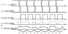
- FIG. 2 shows the frame synchronization signal (I), the X-ray irradiation period (II), the reading period signal (III), the drive voltage (IV) to be originally applied to the Peltier element 92, and the Peltier
- the drive voltage (V) actually applied to the element 92 is displayed with the times matched.
- the controller 7 operates at the H level in the period until the voltage corresponding to all the pixels DU to be read is completely converted to the digital value after the gate driving circuit 5 is operated, and at the L level in other periods.
- the signal (III) is output during the reading period. It is assumed that the frame period is 266 ms and the reading period is about 120 ms.
- the reading period requires (the time when the voltage of the charge amplifier 61 is stabilized + the conversion time of the A / D conversion circuit 62) ⁇ the number of pixels. However, the reading period can be shortened by providing a plurality of A / D conversion circuits and operating them in parallel.
- the software according to the present embodiment includes a feedback control task that repeats the following steps S11 to S15 at a predetermined cycle.
- Step S11 The voltage signal value I ad of the thermistor 91 is read from the A / D conversion circuit 93. Further, the signal (III) during the reading period is read from the controller 7.
- Step S12 previously stored, the value I 1 read from the A / D conversion circuit 93 when the temperature T 1 of the thermistor 91, the A / D conversion circuit 93 when the temperature of the thermistor 91 is T 2
- Step S13 the target temperature T 0, the relationship between the current temperature T, to determine the voltage value V p to be output to the Peltier device.
- ⁇ is a coefficient, and the larger the value, the faster the follow-up, but it also causes hunting.
- the control is PID control, the temperature T from the predetermined number of times to the present is stored in the memory, and the integral value and the differential value are multiplied by the respective coefficients and added to the value of the difference control. That's fine.
- the method of determining V p can be easily replaced by other known control techniques, and how it is determined does not relate to the essence of the present invention, and thus detailed description thereof is omitted.
- Step S15 The determined V p is output to the D / A conversion circuit 94.
- the output V p is stored as V prev .
- the predetermined period is desirably as short as possible within the range of the processing capability of the CPU 90.
- the cycle can be set to about several ms to 20 ms.
- FPGA Field Programmable Gate Array
- the calculation is simply recalculated so that the difference from the previous output value does not exceed a certain threshold, but the history of Vp before a predetermined period is saved and one-dimensional Fourier transform is performed. Later, after removing a frequency component higher than a predetermined threshold, inverse Fourier transform is performed, and Vp is recalculated, which can be replaced with various recalculation methods. That is, as long as the frequency of the driving voltage of the Peltier element 92 during the reading period is set to be lower than (a part of) the other periods, various methods such as recalculation can be changed. Are all included.
- FIG. 3 also shows temporal changes of each signal as in FIG.
- the feedback control task repeatedly executes the following steps S21-24 at a predetermined cycle. Since the configuration other than the program is the same as that of the first embodiment, the description thereof is omitted.
- Step S21 The voltage signal value I ad of the thermistor 91 is read from the A / D conversion circuit 93.
- Step S22 Since this is the same as Step S12 in the first embodiment, description thereof will be omitted.
- Step S23 Since this is the same as Step S13 in the first embodiment, a description thereof will be omitted.
- Step S24 The determined V p is converted into a duty ratio D and notified to the PWM task. Save V p as V prev .
- the PWM task repeatedly executes the following steps P21 to P25 with a shorter cycle than the feedback control task.
- Step P21 The reading period signal (III) is read from the controller 7.
- Step P22 The voltage V s to be output to the D / A conversion circuit 94 is determined as follows.
- C is a counter variable.
- C max is the maximum value of C and corresponds to the resolution of the PWM waveform.
- Step P23 When the signal (III) during the reading period is at the H level (section B in FIG. 2), V s is replaced with V sprev which is the previous V s . That is, during a read period signal (III) is such that will not change in the future state of V s at the H level.
- Step P24 Further, the determined V s is output to the D / A conversion circuit 94.
- the output V s is stored as V sprev .
- Step P25 C is incremented. If C> C max , 0 is substituted for C.
- PWM control can be performed without changing the value.
- the PWM control cycle and the frame synchronization signal cycle can be controlled completely independently, which is also effective from the viewpoint of control independence.
- FIG. 4 shows temporal changes of each signal as in FIG.
- the program of the present embodiment is the same as that of the second embodiment, and only the operation of the controller 7 is different.
- the controller 7 sequentially operates the gate drive circuit 5. At this time, each time the gate line G is driven in a predetermined row, a short-term weight is inserted. In this state, a reading period in which the gate line G is driven to the H level in the period from when the voltage corresponding to the pixel DU in the predetermined row is completely converted to the digital value, and is set to the L level in other periods.
- the middle signal (III) is output (FIG. 4). Then, the period B in which the signal state can be displaced is dispersed.
- the predetermined line may be one line or about half of all the lines. As long as X-ray irradiation and reading operations can be performed within the frame period, it is desirable to insert as many weights as possible with as few predetermined rows as possible.
- FIG. 5 shows a configuration in which the same functions as in the second to third embodiments are realized by hardware as a fourth embodiment.
- the configuration other than the temperature control means 9 in this embodiment and the feedback control method for determining the output with the digital value from the A / D conversion circuit 93 as the input are the same as in the other embodiments, and will be described. Is omitted.
- the temperature control means 9 includes a thermistor 91, a Peltier element 92, an A / D conversion circuit 93 that converts the voltage signal of the thermistor 91 into a digital value, and a drive voltage of the Peltier element 92 in a PWM waveform.
- a CPU 90 The software installed in the CPU 90 receives the digital value from the A / D conversion circuit 93 as an input, calculates the duty ratio for the PWM control circuit 96, and outputs it. With this function, power consumption can be minimized and noise superposition due to driving of the Peltier element can be eliminated.
Landscapes
- Physics & Mathematics (AREA)
- Health & Medical Sciences (AREA)
- Life Sciences & Earth Sciences (AREA)
- General Physics & Mathematics (AREA)
- High Energy & Nuclear Physics (AREA)
- Molecular Biology (AREA)
- Spectroscopy & Molecular Physics (AREA)
- Apparatus For Radiation Diagnosis (AREA)
- Measurement Of Radiation (AREA)
- Transforming Light Signals Into Electric Signals (AREA)
- Solid State Image Pick-Up Elements (AREA)
Abstract
Priority Applications (5)
| Application Number | Priority Date | Filing Date | Title |
|---|---|---|---|
| US12/934,503 US8426825B2 (en) | 2008-03-25 | 2008-03-25 | Radiation image pickup device |
| PCT/JP2008/055595 WO2009118832A1 (fr) | 2008-03-25 | 2008-03-25 | Dispositif de saisie d'images d'un rayonnement |
| JP2010505073A JP4775509B2 (ja) | 2008-03-25 | 2008-03-25 | 放射線撮像装置 |
| CN200880129446.7A CN102047144B (zh) | 2008-03-25 | 2008-03-25 | 放射线成像装置 |
| EP08722805A EP2259088A1 (fr) | 2008-03-25 | 2008-03-25 | Dispositif de saisie d'images d'un rayonnement |
Applications Claiming Priority (1)
| Application Number | Priority Date | Filing Date | Title |
|---|---|---|---|
| PCT/JP2008/055595 WO2009118832A1 (fr) | 2008-03-25 | 2008-03-25 | Dispositif de saisie d'images d'un rayonnement |
Publications (1)
| Publication Number | Publication Date |
|---|---|
| WO2009118832A1 true WO2009118832A1 (fr) | 2009-10-01 |
Family
ID=41113073
Family Applications (1)
| Application Number | Title | Priority Date | Filing Date |
|---|---|---|---|
| PCT/JP2008/055595 Ceased WO2009118832A1 (fr) | 2008-03-25 | 2008-03-25 | Dispositif de saisie d'images d'un rayonnement |
Country Status (5)
| Country | Link |
|---|---|
| US (1) | US8426825B2 (fr) |
| EP (1) | EP2259088A1 (fr) |
| JP (1) | JP4775509B2 (fr) |
| CN (1) | CN102047144B (fr) |
| WO (1) | WO2009118832A1 (fr) |
Cited By (4)
| Publication number | Priority date | Publication date | Assignee | Title |
|---|---|---|---|---|
| JP2011138879A (ja) * | 2009-12-28 | 2011-07-14 | Nec Toshiba Space Systems Ltd | デバイス設置構造 |
| WO2012014251A1 (fr) * | 2010-07-26 | 2012-02-02 | 株式会社島津製作所 | Détecteur d'images bidimensionnelles |
| JP2012205194A (ja) * | 2011-03-28 | 2012-10-22 | Fujifilm Corp | 撮影装置、撮影プログラム、及び撮影方法 |
| JP2013170922A (ja) * | 2012-02-21 | 2013-09-02 | Ge Medical Systems Global Technology Co Llc | 放射線検出装置および放射線撮影装置 |
Families Citing this family (1)
| Publication number | Priority date | Publication date | Assignee | Title |
|---|---|---|---|---|
| DE102012213404B3 (de) * | 2012-07-31 | 2014-01-23 | Siemens Aktiengesellschaft | Verfahren zur Temperaturstabilisierung, Röntgenstrahlungsdetektor und CT-System |
Citations (5)
| Publication number | Priority date | Publication date | Assignee | Title |
|---|---|---|---|---|
| JPH11271456A (ja) * | 1998-03-23 | 1999-10-08 | Toshiba Corp | 平面検出器 |
| JPH11344573A (ja) * | 1998-06-02 | 1999-12-14 | Toshiba Corp | 放射線半導体検出器および放射線半導体検出器アレイ |
| JP2003014860A (ja) | 2001-06-29 | 2003-01-15 | Toshiba Corp | 放射線検出器および放射線検査装置 |
| JP2005128000A (ja) * | 2003-09-30 | 2005-05-19 | Hitachi Ltd | 核医学診断装置 |
| JP2006325631A (ja) | 2005-05-23 | 2006-12-07 | Shimadzu Corp | 撮像装置 |
Family Cites Families (3)
| Publication number | Priority date | Publication date | Assignee | Title |
|---|---|---|---|---|
| EP0342155A3 (fr) * | 1988-05-13 | 1990-06-27 | Agrogen-Stiftung | Appareil de laboratoire pour chauffer ou refroidir à volonté |
| US20050067579A1 (en) * | 2003-09-30 | 2005-03-31 | Katsutoshi Tsuchiya | Nuclear medicine imaging apparatus |
| JP4649940B2 (ja) * | 2004-10-14 | 2011-03-16 | ダイキン工業株式会社 | コンバータの制御方法及びコンバータの制御装置 |
-
2008
- 2008-03-25 WO PCT/JP2008/055595 patent/WO2009118832A1/fr not_active Ceased
- 2008-03-25 EP EP08722805A patent/EP2259088A1/fr not_active Withdrawn
- 2008-03-25 JP JP2010505073A patent/JP4775509B2/ja active Active
- 2008-03-25 CN CN200880129446.7A patent/CN102047144B/zh not_active Expired - Fee Related
- 2008-03-25 US US12/934,503 patent/US8426825B2/en not_active Expired - Fee Related
Patent Citations (5)
| Publication number | Priority date | Publication date | Assignee | Title |
|---|---|---|---|---|
| JPH11271456A (ja) * | 1998-03-23 | 1999-10-08 | Toshiba Corp | 平面検出器 |
| JPH11344573A (ja) * | 1998-06-02 | 1999-12-14 | Toshiba Corp | 放射線半導体検出器および放射線半導体検出器アレイ |
| JP2003014860A (ja) | 2001-06-29 | 2003-01-15 | Toshiba Corp | 放射線検出器および放射線検査装置 |
| JP2005128000A (ja) * | 2003-09-30 | 2005-05-19 | Hitachi Ltd | 核医学診断装置 |
| JP2006325631A (ja) | 2005-05-23 | 2006-12-07 | Shimadzu Corp | 撮像装置 |
Cited By (5)
| Publication number | Priority date | Publication date | Assignee | Title |
|---|---|---|---|---|
| JP2011138879A (ja) * | 2009-12-28 | 2011-07-14 | Nec Toshiba Space Systems Ltd | デバイス設置構造 |
| WO2012014251A1 (fr) * | 2010-07-26 | 2012-02-02 | 株式会社島津製作所 | Détecteur d'images bidimensionnelles |
| JP5549731B2 (ja) * | 2010-07-26 | 2014-07-16 | 株式会社島津製作所 | 二次元画像検出器 |
| JP2012205194A (ja) * | 2011-03-28 | 2012-10-22 | Fujifilm Corp | 撮影装置、撮影プログラム、及び撮影方法 |
| JP2013170922A (ja) * | 2012-02-21 | 2013-09-02 | Ge Medical Systems Global Technology Co Llc | 放射線検出装置および放射線撮影装置 |
Also Published As
| Publication number | Publication date |
|---|---|
| US8426825B2 (en) | 2013-04-23 |
| CN102047144B (zh) | 2014-05-07 |
| EP2259088A1 (fr) | 2010-12-08 |
| US20110024643A1 (en) | 2011-02-03 |
| CN102047144A (zh) | 2011-05-04 |
| JPWO2009118832A1 (ja) | 2011-07-21 |
| JP4775509B2 (ja) | 2011-09-21 |
Similar Documents
| Publication | Publication Date | Title |
|---|---|---|
| JP4775509B2 (ja) | 放射線撮像装置 | |
| JP5935284B2 (ja) | 撮像装置および撮像表示システム | |
| RU2504101C2 (ru) | Устройство формирования изображений и система формирования изображений, способ формирования изображений и программа формирования изображений | |
| RU2356178C2 (ru) | Устройство формирования изображений методом излучения, способ возбуждения этого устройства и система формирования изображений методом излучения | |
| EP2274903B1 (fr) | Pixels de capteur à gain ajustable, matrices et systèmes de matrice et procédés apparentés | |
| JP6148227B2 (ja) | アクティブ検出マトリックス用の制御回路のラインをアドレス指定する装置 | |
| EP2560373B1 (fr) | Unité de capture d'image et système de capture d'image et d'affichage | |
| US20070183573A1 (en) | Imaging apparatus and imaging system | |
| JP5935286B2 (ja) | 撮像装置および撮像表示システム | |
| WO2011048629A1 (fr) | Dispositif d'imagerie par rayonnement | |
| JP2004037382A (ja) | 放射線検出器及び放射線診断装置 | |
| JP4888599B2 (ja) | 光または放射線撮像装置 | |
| JP2014192825A (ja) | 撮像装置および撮像表示システム | |
| JP5935285B2 (ja) | 撮像装置および撮像表示システム | |
| JP2003256820A (ja) | 画像読取装置及びその感度設定方法 | |
| CN114096886B (zh) | 距离图像测量装置 | |
| CN107242878B (zh) | 放射线成像装置和操作该装置的方法、放射线成像系统 | |
| JP4862767B2 (ja) | X線診断装置 | |
| CN102905087A (zh) | 固态成像装置和模数转换输出位计数控制方法 | |
| EP2202961A2 (fr) | Détecteur à rayons X et son procédé de commande | |
| JP2013026912A (ja) | X線平面検出器およびその駆動方法 | |
| KR101427022B1 (ko) | 방사선 평면검출기의 리프레시 동작방법 | |
| JP2015112459A (ja) | X線診断装置 | |
| US12008834B2 (en) | Ultrasonic sensor device and method of controlling the same | |
| CN110166717B (zh) | 图像传感器以及驱动图像传感器的方法 |
Legal Events
| Date | Code | Title | Description |
|---|---|---|---|
| WWE | Wipo information: entry into national phase |
Ref document number: 200880129446.7 Country of ref document: CN |
|
| 121 | Ep: the epo has been informed by wipo that ep was designated in this application |
Ref document number: 08722805 Country of ref document: EP Kind code of ref document: A1 |
|
| WWE | Wipo information: entry into national phase |
Ref document number: 2010505073 Country of ref document: JP |
|
| WWE | Wipo information: entry into national phase |
Ref document number: 2008722805 Country of ref document: EP |
|
| NENP | Non-entry into the national phase |
Ref country code: DE |
|
| WWE | Wipo information: entry into national phase |
Ref document number: 12934503 Country of ref document: US |