WO2009128247A1 - プラズマディスプレイ装置 - Google Patents
プラズマディスプレイ装置 Download PDFInfo
- Publication number
- WO2009128247A1 WO2009128247A1 PCT/JP2009/001703 JP2009001703W WO2009128247A1 WO 2009128247 A1 WO2009128247 A1 WO 2009128247A1 JP 2009001703 W JP2009001703 W JP 2009001703W WO 2009128247 A1 WO2009128247 A1 WO 2009128247A1
- Authority
- WO
- WIPO (PCT)
- Prior art keywords
- period
- discharge
- sustain
- voltage
- panel
- Prior art date
- Legal status (The legal status is an assumption and is not a legal conclusion. Google has not performed a legal analysis and makes no representation as to the accuracy of the status listed.)
- Ceased
Links
Images






Classifications
-
- H—ELECTRICITY
- H01—ELECTRIC ELEMENTS
- H01J—ELECTRIC DISCHARGE TUBES OR DISCHARGE LAMPS
- H01J11/00—Gas-filled discharge tubes with alternating current induction of the discharge, e.g. alternating current plasma display panels [AC-PDP]; Gas-filled discharge tubes without any main electrode inside the vessel; Gas-filled discharge tubes with at least one main electrode outside the vessel
- H01J11/10—AC-PDPs with at least one main electrode being out of contact with the plasma
- H01J11/12—AC-PDPs with at least one main electrode being out of contact with the plasma with main electrodes provided on both sides of the discharge space
-
- G—PHYSICS
- G09—EDUCATION; CRYPTOGRAPHY; DISPLAY; ADVERTISING; SEALS
- G09G—ARRANGEMENTS OR CIRCUITS FOR CONTROL OF INDICATING DEVICES USING STATIC MEANS TO PRESENT VARIABLE INFORMATION
- G09G3/00—Control arrangements or circuits, of interest only in connection with visual indicators other than cathode-ray tubes
- G09G3/20—Control arrangements or circuits, of interest only in connection with visual indicators other than cathode-ray tubes for presentation of an assembly of a number of characters, e.g. a page, by composing the assembly by combination of individual elements arranged in a matrix no fixed position being assigned to or needed to be assigned to the individual characters or partial characters
- G09G3/22—Control arrangements or circuits, of interest only in connection with visual indicators other than cathode-ray tubes for presentation of an assembly of a number of characters, e.g. a page, by composing the assembly by combination of individual elements arranged in a matrix no fixed position being assigned to or needed to be assigned to the individual characters or partial characters using controlled light sources
- G09G3/28—Control arrangements or circuits, of interest only in connection with visual indicators other than cathode-ray tubes for presentation of an assembly of a number of characters, e.g. a page, by composing the assembly by combination of individual elements arranged in a matrix no fixed position being assigned to or needed to be assigned to the individual characters or partial characters using controlled light sources using luminous gas-discharge panels, e.g. plasma panels
- G09G3/288—Control arrangements or circuits, of interest only in connection with visual indicators other than cathode-ray tubes for presentation of an assembly of a number of characters, e.g. a page, by composing the assembly by combination of individual elements arranged in a matrix no fixed position being assigned to or needed to be assigned to the individual characters or partial characters using controlled light sources using luminous gas-discharge panels, e.g. plasma panels using AC panels
- G09G3/291—Control arrangements or circuits, of interest only in connection with visual indicators other than cathode-ray tubes for presentation of an assembly of a number of characters, e.g. a page, by composing the assembly by combination of individual elements arranged in a matrix no fixed position being assigned to or needed to be assigned to the individual characters or partial characters using controlled light sources using luminous gas-discharge panels, e.g. plasma panels using AC panels controlling the gas discharge to control a cell condition, e.g. by means of specific pulse shapes
-
- G—PHYSICS
- G09—EDUCATION; CRYPTOGRAPHY; DISPLAY; ADVERTISING; SEALS
- G09G—ARRANGEMENTS OR CIRCUITS FOR CONTROL OF INDICATING DEVICES USING STATIC MEANS TO PRESENT VARIABLE INFORMATION
- G09G3/00—Control arrangements or circuits, of interest only in connection with visual indicators other than cathode-ray tubes
- G09G3/20—Control arrangements or circuits, of interest only in connection with visual indicators other than cathode-ray tubes for presentation of an assembly of a number of characters, e.g. a page, by composing the assembly by combination of individual elements arranged in a matrix no fixed position being assigned to or needed to be assigned to the individual characters or partial characters
- G09G3/22—Control arrangements or circuits, of interest only in connection with visual indicators other than cathode-ray tubes for presentation of an assembly of a number of characters, e.g. a page, by composing the assembly by combination of individual elements arranged in a matrix no fixed position being assigned to or needed to be assigned to the individual characters or partial characters using controlled light sources
- G09G3/28—Control arrangements or circuits, of interest only in connection with visual indicators other than cathode-ray tubes for presentation of an assembly of a number of characters, e.g. a page, by composing the assembly by combination of individual elements arranged in a matrix no fixed position being assigned to or needed to be assigned to the individual characters or partial characters using controlled light sources using luminous gas-discharge panels, e.g. plasma panels
- G09G3/288—Control arrangements or circuits, of interest only in connection with visual indicators other than cathode-ray tubes for presentation of an assembly of a number of characters, e.g. a page, by composing the assembly by combination of individual elements arranged in a matrix no fixed position being assigned to or needed to be assigned to the individual characters or partial characters using controlled light sources using luminous gas-discharge panels, e.g. plasma panels using AC panels
- G09G3/291—Control arrangements or circuits, of interest only in connection with visual indicators other than cathode-ray tubes for presentation of an assembly of a number of characters, e.g. a page, by composing the assembly by combination of individual elements arranged in a matrix no fixed position being assigned to or needed to be assigned to the individual characters or partial characters using controlled light sources using luminous gas-discharge panels, e.g. plasma panels using AC panels controlling the gas discharge to control a cell condition, e.g. by means of specific pulse shapes
- G09G3/293—Control arrangements or circuits, of interest only in connection with visual indicators other than cathode-ray tubes for presentation of an assembly of a number of characters, e.g. a page, by composing the assembly by combination of individual elements arranged in a matrix no fixed position being assigned to or needed to be assigned to the individual characters or partial characters using controlled light sources using luminous gas-discharge panels, e.g. plasma panels using AC panels controlling the gas discharge to control a cell condition, e.g. by means of specific pulse shapes for address discharge
- G09G3/2935—Addressed by erasing selected cells that are in an ON state
-
- G—PHYSICS
- G09—EDUCATION; CRYPTOGRAPHY; DISPLAY; ADVERTISING; SEALS
- G09G—ARRANGEMENTS OR CIRCUITS FOR CONTROL OF INDICATING DEVICES USING STATIC MEANS TO PRESENT VARIABLE INFORMATION
- G09G3/00—Control arrangements or circuits, of interest only in connection with visual indicators other than cathode-ray tubes
- G09G3/20—Control arrangements or circuits, of interest only in connection with visual indicators other than cathode-ray tubes for presentation of an assembly of a number of characters, e.g. a page, by composing the assembly by combination of individual elements arranged in a matrix no fixed position being assigned to or needed to be assigned to the individual characters or partial characters
- G09G3/22—Control arrangements or circuits, of interest only in connection with visual indicators other than cathode-ray tubes for presentation of an assembly of a number of characters, e.g. a page, by composing the assembly by combination of individual elements arranged in a matrix no fixed position being assigned to or needed to be assigned to the individual characters or partial characters using controlled light sources
- G09G3/28—Control arrangements or circuits, of interest only in connection with visual indicators other than cathode-ray tubes for presentation of an assembly of a number of characters, e.g. a page, by composing the assembly by combination of individual elements arranged in a matrix no fixed position being assigned to or needed to be assigned to the individual characters or partial characters using controlled light sources using luminous gas-discharge panels, e.g. plasma panels
- G09G3/288—Control arrangements or circuits, of interest only in connection with visual indicators other than cathode-ray tubes for presentation of an assembly of a number of characters, e.g. a page, by composing the assembly by combination of individual elements arranged in a matrix no fixed position being assigned to or needed to be assigned to the individual characters or partial characters using controlled light sources using luminous gas-discharge panels, e.g. plasma panels using AC panels
- G09G3/296—Driving circuits for producing the waveforms applied to the driving electrodes
-
- H—ELECTRICITY
- H01—ELECTRIC ELEMENTS
- H01J—ELECTRIC DISCHARGE TUBES OR DISCHARGE LAMPS
- H01J11/00—Gas-filled discharge tubes with alternating current induction of the discharge, e.g. alternating current plasma display panels [AC-PDP]; Gas-filled discharge tubes without any main electrode inside the vessel; Gas-filled discharge tubes with at least one main electrode outside the vessel
- H01J11/20—Constructional details
- H01J11/34—Vessels, containers or parts thereof, e.g. substrates
- H01J11/40—Layers for protecting or enhancing the electron emission, e.g. MgO layers
-
- G—PHYSICS
- G09—EDUCATION; CRYPTOGRAPHY; DISPLAY; ADVERTISING; SEALS
- G09G—ARRANGEMENTS OR CIRCUITS FOR CONTROL OF INDICATING DEVICES USING STATIC MEANS TO PRESENT VARIABLE INFORMATION
- G09G2310/00—Command of the display device
- G09G2310/02—Addressing, scanning or driving the display screen or processing steps related thereto
- G09G2310/0202—Addressing of scan or signal lines
- G09G2310/0216—Interleaved control phases for different scan lines in the same sub-field, e.g. initialization, addressing and sustaining in plasma displays that are not simultaneous for all scan lines
-
- G—PHYSICS
- G09—EDUCATION; CRYPTOGRAPHY; DISPLAY; ADVERTISING; SEALS
- G09G—ARRANGEMENTS OR CIRCUITS FOR CONTROL OF INDICATING DEVICES USING STATIC MEANS TO PRESENT VARIABLE INFORMATION
- G09G2310/00—Command of the display device
- G09G2310/02—Addressing, scanning or driving the display screen or processing steps related thereto
- G09G2310/0202—Addressing of scan or signal lines
- G09G2310/0218—Addressing of scan or signal lines with collection of electrodes in groups for n-dimensional addressing
-
- G—PHYSICS
- G09—EDUCATION; CRYPTOGRAPHY; DISPLAY; ADVERTISING; SEALS
- G09G—ARRANGEMENTS OR CIRCUITS FOR CONTROL OF INDICATING DEVICES USING STATIC MEANS TO PRESENT VARIABLE INFORMATION
- G09G3/00—Control arrangements or circuits, of interest only in connection with visual indicators other than cathode-ray tubes
- G09G3/20—Control arrangements or circuits, of interest only in connection with visual indicators other than cathode-ray tubes for presentation of an assembly of a number of characters, e.g. a page, by composing the assembly by combination of individual elements arranged in a matrix no fixed position being assigned to or needed to be assigned to the individual characters or partial characters
- G09G3/22—Control arrangements or circuits, of interest only in connection with visual indicators other than cathode-ray tubes for presentation of an assembly of a number of characters, e.g. a page, by composing the assembly by combination of individual elements arranged in a matrix no fixed position being assigned to or needed to be assigned to the individual characters or partial characters using controlled light sources
- G09G3/28—Control arrangements or circuits, of interest only in connection with visual indicators other than cathode-ray tubes for presentation of an assembly of a number of characters, e.g. a page, by composing the assembly by combination of individual elements arranged in a matrix no fixed position being assigned to or needed to be assigned to the individual characters or partial characters using controlled light sources using luminous gas-discharge panels, e.g. plasma panels
- G09G3/288—Control arrangements or circuits, of interest only in connection with visual indicators other than cathode-ray tubes for presentation of an assembly of a number of characters, e.g. a page, by composing the assembly by combination of individual elements arranged in a matrix no fixed position being assigned to or needed to be assigned to the individual characters or partial characters using controlled light sources using luminous gas-discharge panels, e.g. plasma panels using AC panels
- G09G3/296—Driving circuits for producing the waveforms applied to the driving electrodes
- G09G3/2965—Driving circuits for producing the waveforms applied to the driving electrodes using inductors for energy recovery
Definitions
- the present invention relates to a plasma display device which is an image display device using a plasma display panel.
- Plasma display panels are capable of high-speed display among thin image display elements and are easy to increase in size, and thus are put into practical use as large-screen display devices.
- the panel consists of a front plate and a back plate bonded together.
- the front plate is formed on a glass substrate, a display electrode pair formed of a scan electrode and a sustain electrode formed on the glass substrate, a dielectric layer formed so as to cover the display electrode pair, and the dielectric layer And a protective layer.
- the protective layer is provided for the purpose of protecting the dielectric layer from ion collision and facilitating discharge.
- the back plate includes a glass substrate, a data electrode formed on the glass substrate, a dielectric layer covering the data electrode, a partition formed on the dielectric layer, and red, green and blue formed between the partitions. And a phosphor layer that emits light.
- the front plate and the rear plate face each other so that the display electrode pair and the data electrode intersect with each other across the discharge space, and the periphery is sealed with a low-melting glass.
- a discharge gas containing xenon is sealed in the discharge space.
- a discharge cell is formed in a portion where the display electrode pair and the data electrode face each other.
- the plasma display device using the panel having such a configuration selectively generates gas discharge in each discharge cell of the panel, and excites and emits phosphors of red, green, and blue colors by ultraviolet rays generated at this time. Color display is performed.
- the subfield method is mainly used as a method for displaying an image on a plasma display device using such a panel.
- one field period is formed by a plurality of subfields having luminance weights defined in advance, and an image is displayed by controlling light emission / non-light emission of each discharge cell in each subfield.
- the number of subfields constituting one field period may be increased.
- the above-described subfield method is a method in which one field period is composed of a plurality of subfields having an initialization period, an address period, and a sustain period, and gradation display is performed by a combination of subfields that emit light.
- it is necessary to perform a reliable write operation within a short time. Therefore, development of a panel capable of high-speed driving is being promoted, and studies on a driving method and a driving circuit for displaying a high-quality image taking advantage of the features of the panel are being advanced.
- Patent Document 2 discloses a panel in which a magnesium oxide layer having a cathodoluminescence emission peak at 200 to 300 nm is formed by vapor-phase oxidation of magnesium vapor, and a display electrode that forms all display lines in an address period
- a plasma display device including an electrode driving circuit that sequentially applies a scan pulse to one of each pair and supplies an address pulse corresponding to a display line to which the scan pulse is applied to a data electrode.
- the present invention includes a front plate in which a display electrode pair is formed on a first glass substrate, a dielectric layer is formed so as to cover the display electrode pair, and a protective layer is formed on the dielectric layer, and a second glass substrate A panel on which a back plate on which data electrodes are formed is placed opposite to each other, a discharge cell is formed at a position where the display electrode pair and the data electrode face each other, an address period in which an address discharge is generated in the discharge cell, and a sustain discharge.
- a plasma display device comprising a panel driving circuit for driving a panel by temporally arranging a plurality of subfields having a sustain period to form one field period, wherein the protective layer is formed of a metal oxide And a particle layer formed by adhering agglomerated particles obtained by aggregating a plurality of magnesium oxide single crystal particles to the underlying protective layer. It is configured to drive the panel by generating an initializing discharge for forming wall charges in the first subfield of the bfield and generating an address discharge for erasing the wall charges in the address period of the plurality of subfields.
- FIG. 1 is an exploded perspective view showing the structure of the panel according to Embodiment 1 of the present invention.
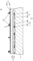
- FIG. 2 is a cross-sectional view showing the configuration of the front plate of the panel.
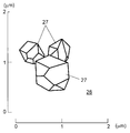
- FIG. 3 is a view showing an example of the aggregated particles of the panel.
- FIG. 4 is a diagram showing electron emission performance and charge retention performance of a prototype panel including the panel.
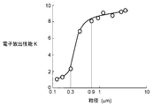
- FIG. 5A is a diagram showing experimental results of examining the electron emission performance by changing the particle size of the single crystal particles of the prototype panel.
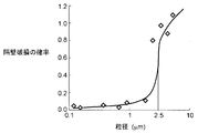
- FIG. 5B is a diagram showing the relationship between the grain size of the single crystal particles of the prototype panel and the breakage of the partition walls.
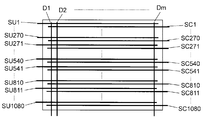
- FIG. 6 is a diagram showing the electrode arrangement of the panel in accordance with the first exemplary embodiment of the present invention.
- FIG. 1 is an exploded perspective view showing the structure of the panel according to Embodiment 1 of the present invention.
- FIG. 2 is a cross-sectional view showing the configuration of the front plate of the panel.
- FIG. 7 is a drive voltage waveform diagram applied to each electrode of the panel.
- FIG. 8 is a diagram showing an electrode arrangement of the panel in accordance with the second exemplary embodiment.
- FIG. 9 is a drive voltage waveform diagram applied to each electrode of the panel.
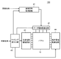
- FIG. 10 is a circuit block diagram of the plasma display device according to the first and second embodiments of the present invention.
- FIG. 11 is a circuit diagram of a scan electrode drive circuit and a sustain electrode drive circuit of the plasma display device.
- SYMBOLS 10 Panel 20 Front plate 21 (1st) Glass substrate 22 Scan electrode 22a, 23a Transparent electrode 22b, 23b Bus electrode 23 Sustain electrode 24 Display electrode pair 25 Dielectric layer 26 Protection layer 26a Underlayer protection layer 26b Particle layer 27 Single crystal Particle 28 Aggregated particle 30 Back plate 31 (Second) glass substrate 32 Data electrode 34 Partition 35 Phosphor layer 41 Image signal processing circuit 42 Data electrode drive circuit 43 Scan electrode drive circuit 44 Sustain electrode drive circuit 45 Timing generation circuit 50, 80 Sustain pulse generation circuit 60 Initialization waveform generation circuit 70 Scanning pulse generation circuit 100 Plasma display device
- FIG. 1 is an exploded perspective view showing the structure of panel 10 according to Embodiment 1 of the present invention.
- a front plate 20 and a back plate 30 are disposed so as to face each other, and an outer peripheral portion thereof is sealed with a low-melting glass sealing material.
- the discharge space 15 inside the panel 10 is filled with a discharge gas such as xenon at a pressure of 400 Torr to 600 Torr.
- a plurality of display electrode pairs 24 including the scanning electrodes 22 and the sustain electrodes 23 are formed in parallel.
- a dielectric layer 25 is formed on the glass substrate 21 so as to cover the display electrode pair 24, and a protective layer 26 mainly composed of magnesium oxide is formed on the dielectric layer 25.
- a plurality of data electrodes 32 are formed in parallel to each other in a direction orthogonal to the display electrode pair 24, and this is covered with the dielectric layer 33. ing. Further, a partition wall 34 is formed on the dielectric layer 33. A phosphor layer 35 that emits red, green, and blue light by ultraviolet rays is formed on the dielectric layer 33 and on the side surfaces of the partition wall 34.
- a discharge cell is formed at a position where the display electrode pair 24 and the data electrode 32 intersect with each other, and a set of discharge cells having red, green, and blue phosphor layers 35 is a pixel for color display.
- the dielectric layer 33 is not essential, and a configuration in which the dielectric layer 33 is omitted may be used.
- FIG. 2 is a cross-sectional view showing the configuration of the front plate 20 of the panel 10 according to Embodiment 1 of the present invention, which is shown upside down with respect to the front plate 20 shown in FIG.
- a display electrode pair 24 including a scan electrode 22 and a sustain electrode 23 is formed on the glass substrate 21, a display electrode pair 24 including a scan electrode 22 and a sustain electrode 23 is formed.
- the scan electrode 22 includes a transparent electrode 22a formed from indium tin oxide, tin oxide, or the like, and a bus electrode 22b formed on the transparent electrode 22a.
- the sustain electrode 23 includes a transparent electrode 23a and a bus electrode 23b formed thereon.
- the bus electrode 22b and the bus electrode 23b are provided to impart conductivity in the longitudinal direction of the transparent electrode 22a and the transparent electrode 23a, and are formed of a conductive material mainly composed of silver.
- the dielectric layer 25 includes a first dielectric layer 25a formed so as to cover the transparent electrode 22a, the transparent electrode 23a, the bus electrode 22b, and the bus electrode 23b, and the first dielectric layer 25a.
- This is a two-layer structure of the second dielectric layer 25b formed in the above.
- the dielectric layer 25 does not necessarily have a two-layer structure, and may have a single-layer structure or a structure of three or more layers.
- a protective layer 26 is formed on the dielectric layer 25. Details of the protective layer 26 will be described below.
- the protective layer 26 is a base protection formed on the second dielectric layer 25b.
- the layer 26a is composed of a particle layer 26b formed on the base protective layer 26a.
- the base protective layer 26a is a thin film containing magnesium oxide as a main component, and its thickness is, for example, 0.3 ⁇ m to 1.0 ⁇ m.
- the particle layer 26b is configured by discretely adhering aggregated particles 28 in which a plurality of magnesium oxide single crystal particles 27 are aggregated so as to be distributed almost uniformly over the entire surface of the base protective layer 26a.
- the aggregated particles 28 are shown enlarged.
- FIG. 3 is a diagram showing an example of the aggregated particles 28 of the panel 10 according to Embodiment 1 of the present invention.
- the agglomerated particles 28 are those in which the single crystal particles 27 are aggregated or necked as described above, and a plurality of single crystal particles 27 form an aggregate due to static electricity, van der Waals force, or the like.
- the single crystal particles 27 preferably have a polyhedral shape having seven or more faces such as a tetrahedron and a dodecahedron, and a particle diameter of about 0.9 ⁇ m to 2.0 ⁇ m.
- the aggregated particles 28 are preferably those in which 2 to 5 single crystal particles 27 are aggregated, and the aggregated particles 28 preferably have a particle size of about 0.3 ⁇ m to 5 ⁇ m.
- the single crystal particles 27 satisfying the above-described conditions and the aggregated particles 28 obtained by aggregating them can be generated as follows.
- a magnesium oxide precursor such as magnesium carbonate or magnesium hydroxide
- the particle size is controlled to about 0.3 ⁇ m to 2 ⁇ m by setting the firing temperature to a relatively high 1000 ° C. or higher. Can do.
- aggregated particles 28 in which the single crystal particles 27 are aggregated or necked can be obtained.
- the first type of trial panel is a panel provided with a protective layer made only of a thin base protective layer 26a mainly composed of magnesium oxide.
- the second type of prototype panel is a panel in which magnesium oxide single crystal particles 27 are dispersed and adhered on a thin base protective layer 26a mainly composed of magnesium oxide without being agglomerated.
- the third type of prototype panel is a panel according to the present embodiment. Magnesium oxide single crystal particles 27 are agglomerated on a thin base protective layer 26a mainly composed of magnesium oxide, so that the aggregated particles 28 are almost entirely covered.
- the panel is discretely attached so as to be uniformly distributed.
- the minimum voltage Vmin of the scanning pulse necessary for driving each panel is used as a numerical value indicating the charge holding performance. Therefore, the smaller the voltage Vmin, the higher the charge retention performance.
- FIG. 4 is a diagram showing the electron emission performance and the charge retention performance of the three types of prototype panels 11 to 13 including the panel according to Embodiment 1 of the present invention.
- the first type prototype panel 11 has a low voltage Vmin and a low numerical value K. Therefore, it can be seen that the panel has high charge retention performance but low electron emission performance.
- the second type of trial panel 12 is high in both voltage Vmin and numerical value K. Therefore, the panel has high electron emission performance but low charge retention performance.
- the third type prototype panel 13 in the present embodiment has a low voltage Vmin and a high value K. Therefore, it can be seen that the panel 10 has good characteristics with high electron emission performance and high charge retention performance.
- the base protective layer 26a which is a thin film mainly composed of magnesium oxide, and the magnesium oxide single crystal particles 27 are aggregated on the base protective layer 26a so that the aggregated particles 28 are distributed almost uniformly over the entire surface.
- the protective layer 26 having the adhered particle layer 26b it is possible to obtain a panel exhibiting good characteristics with high electron emission performance and high charge retention performance.
- the particle size of the single crystal particles 27 will be described.
- the particle diameter means the median diameter.
- FIG. 5A is a diagram showing an experimental result of examining the electron emission performance of the prototype panel 13 by changing the particle size of the single crystal particles 27.
- the particle size was measured by observing the single crystal particles 27 with an electron microscope. Experiments have shown that when the particle size of the single crystal particles 27 is reduced to about 0.3 ⁇ m, the electron emission performance is lowered, and when the particle size is about 0.9 ⁇ m or more, high electron emission performance is obtained.
- the present inventors have experimentally confirmed that the probability of damaging the top of the partition wall 34 increases when the single crystal particles 27 having a large particle size are present at a position in contact with the top of the partition wall 34 of the back plate 30. .
- 5B is a diagram showing the relationship between the particle diameter of the single crystal particles 27 of the prototype panel 13 and the breakage of the partition walls 34.
- the particle diameter of the single crystal particles 27 is increased to about 2.5 ⁇ m, the probability of partition wall breakage increases rapidly.
- the crystal particle size is smaller than 2.5 ⁇ m, the probability of partition wall breakage is relatively high. It can be seen that it can be kept small.
- the particle size of the single crystal particles 27 is desirably 0.9 ⁇ m or more and 2.5 ⁇ m or less. However, in consideration of manufacturing variations and the like, it is desirable to use aggregated particles 28 of single crystal particles 27 having a particle size in the range of 0.9 ⁇ m to 2 ⁇ m. If the protective layer 26 is configured in this way, the panel 10 can be obtained which has no fear of damaging the partition wall 34, has high electron emission performance, and high charge retention performance.
- the panel 10 using the thin base protective layer 26a mainly composed of magnesium oxide has been described.
- the protective layer 26 is provided for the purpose of protecting the dielectric layer 25 from ion collision and facilitating discharge.
- the protective layer 26 is composed of the base protective layer 26a and the particle layer 26b.
- the base protective layer 26a mainly protects the dielectric layer 25, and the particle layer 26b mainly easily generates discharge.
- the base protective layer 26a may be formed using magnesium oxide containing aluminum, aluminum oxide, or another material containing a metal oxide having high sputtering resistance.
- magnesium oxide containing strontium, calcium, barium, aluminum or the like may be used, and a single crystal mainly composed of strontium oxide, calcium oxide, barium oxide or the like.
- the particle layer 26b may be formed using particles.
- FIG. 6 is a diagram showing an electrode arrangement of panel 10 in accordance with the first exemplary embodiment of the present invention.
- panel 10 n scan electrodes SC1 to SCn (scan electrode 22 in FIG. 1) and n sustain electrodes SU1 to SUn (sustain electrode 23 in FIG. 1) long in the row direction (line direction) are arranged.
- M data electrodes D1 to Dm data electrode 32 in FIG. 1) long in the column direction are arranged.
- M ⁇ n are formed.
- the panel 10 is driven using a subfield method in which a plurality of subfields are temporally arranged to form one field period. That is, one field period is divided into a plurality of subfields, and gradation display is performed by controlling light emission / non-light emission of each discharge cell for each subfield.
- Each subfield has an address period and a sustain period.
- the first subfield has an initialization period.
- ⁇ Initialization discharge is generated in the initialization period, and wall charges necessary for sustain discharge for causing the discharge cells to emit light are formed on each electrode. At the same time, wall charges necessary for address discharge are also formed.
- address discharge is generated in the discharge cells that do not emit light, and wall charges for sustain discharge are erased.
- sustain period a number of sustain pulses corresponding to the luminance weight are alternately applied to the display electrode pairs, and a sustain discharge is generated in the discharge cells that did not generate the address discharge to emit light.
- the driving method according to the present embodiment is characterized in that an initializing period is provided in the first subfield, no initializing period is provided in the subsequent subfields, and an address operation is performed in a discharge cell that does not emit light. It is. Then, the initialization operation is performed in the initialization period of the first subfield, and then the sustain discharge is continuously generated in the discharge cells in which the address operation is not performed to emit light. In the discharge cell that has once performed the address operation, the sustain discharge is not generated until the next initialization operation is performed.
- a driving method for performing gradation display by controlling the subfields in which the discharge cells emit light to be continuous and the subfields in which the discharge cells do not emit light to be continuous will be described below. Abbreviated as “continuous drive method”.
- one field is divided into 14 subfields (first SF, second SF,..., 14th SF), and each subfield is, for example, (1, 1, 1, 1, 3). 5, 5, 8, 16, 16, 20, 22, 28, 64).
- the first SF is a subfield having an initialization period
- the second to fourteenth SFs are subfields having no initialization period.
- FIG. 7 is a waveform diagram of driving voltage applied to each electrode of panel 10 in the first exemplary embodiment of the present invention. First, the first SF having the initialization period will be described.
- first, 0 (V) is applied to the data electrodes D1 to Dm, the voltage Vng is applied to the sustain electrodes SU1 to SUn, and the sustain electrode SU1 is applied to the scan electrodes SC1 to SCn.
- a ramp waveform voltage that gradually rises from a voltage Vi1 that is equal to or lower than the discharge start voltage to a voltage Vi2 that exceeds the discharge start voltage is applied to SUn.
- the wall voltage on the electrode represents a voltage generated by wall charges accumulated on the dielectric layer covering the electrode, the protective layer, the phosphor layer, and the like. In the initialization discharge at this time, the wall voltage is excessively stored in anticipation of optimizing the wall voltage in the second half of the subsequent initialization period.
- voltage Ve is applied to sustain electrodes SU1 to SUn
- scan start voltage is applied to scan electrodes SC1 to SCn from voltage Vi3 that is equal to or lower than the discharge start voltage with respect to sustain electrodes SU1 to SUn.
- a ramp waveform voltage that gradually falls toward the voltage Vi4 exceeding the threshold voltage is applied.
- a weak initializing discharge occurs between scan electrodes SC1 to SCn, sustain electrodes SU1 to SUn, and data electrodes D1 to Dm.
- excessive negative wall voltage on scan electrodes SC1 to SCn and excessive positive wall voltage on sustain electrodes SU1 to SUn are optimized, and wall charges necessary for sustain discharge are formed.
- excessive positive wall voltage on the data electrodes D1 to Dm is also optimized, and wall charges necessary for address discharge are also formed. This completes the initialization operation.
- voltage Ve is applied to sustain electrodes SU1 to SUn, and voltage Vc is applied to scan electrodes SC1 to SCn.
- the write pulse voltage Vd is applied.
- the voltage difference at the intersection between the data electrode Dk and the scan electrode SC1 is the difference between the wall voltage on the data electrode Dk and the wall voltage on the scan electrode SC1 due to the difference between the externally applied voltages (Vd ⁇ Va). It becomes the sum and exceeds the discharge start voltage.
- an address discharge occurs between data electrode Dk and scan electrode SC1 and between sustain electrode SU1 and scan electrode SC1, and the wall voltage on scan electrode SC1 and the wall voltage on sustain electrode SU1 are erased.
- the erasing of the wall voltage at this time means that the wall voltage is weakened to such an extent that no sustain discharge occurs in the sustain period described later.
- a negative wall voltage is accumulated on the data electrode Dk.
- discharge delay time the time from when the scan pulse voltage Va and the address pulse voltage Vd are applied until the address discharge is generated. If the electron emission performance of the panel is low and the discharge delay period is long, the time for applying the scan pulse voltage Va and the address pulse voltage Vd, that is, the scan pulse width and the address pulse width, is set longer in order to perform the address operation reliably. This makes it impossible to perform a write operation at high speed. Also, if the charge retention performance of the panel is low, it is necessary to set the voltage values of the scan pulse voltage Va and the write pulse voltage Vd high in order to compensate for the decrease in wall voltage.
- the scan pulse width and the write pulse width can be set shorter than those of the conventional panel, and the write operation can be performed stably and at high speed.
- the voltage values of the scan pulse voltage Va and the write pulse voltage Vd can be set lower than those of the conventional panel.
- an address operation is performed in which an address discharge is caused in a discharge cell that does not emit light on the first line to erase the wall voltage on each electrode.
- the voltage at the intersection between the data electrodes D1 to Dm to which the address pulse voltage Vd is not applied and the scan electrode SC1 does not exceed the discharge start voltage, so the address discharge does not occur and the wall voltage at the end of the initialization period Is preserved.
- the above address operation is performed up to the discharge cell on the nth line, and the address period ends.
- a sustain discharge occurs between scan electrode SCi and sustain electrode SUi, and phosphor layer 35 emits light due to the ultraviolet rays generated at this time.
- a positive wall voltage is accumulated on scan electrode SCi, and a negative wall voltage is accumulated on sustain electrode SUi. Note that no sustain discharge occurs in the discharge cells that have caused the address discharge in the address period.
- sustain pulse voltage Vs is applied to scan electrodes SC1 to SCn, and 0 (V) is applied to sustain electrodes SU1 to SUn.
- the voltage difference between scan electrode SCi and sustain electrode SUi exceeds the discharge start voltage, so sustain discharge occurs again between scan electrode SCi and sustain electrode SUi, and scan electrode A negative wall voltage is accumulated on SCi, and a positive wall voltage is accumulated on sustain electrode SUi.
- the sustain discharges of the number corresponding to the luminance weight are alternately applied to the sustain electrodes SU1 to SUn and the scan electrodes SC1 to SCn, and a potential difference is given between the electrodes of the display electrode pair, so that the address discharge is performed in the address period.
- the sustain discharge is continuously performed in the discharge cells that did not cause the failure.
- the subsequent second SF is a subfield having no initialization period.
- voltage Ve is applied to sustain electrodes SU1 to SUn
- voltage Vc is applied to scan electrodes SC1 to SCn.
- a negative scan pulse voltage Va is applied to the scan electrode SC1 of the first line
- a positive address pulse voltage Vd is applied to the data electrode Dk of the discharge cell that does not emit light in the first line among the data electrodes D1 to Dm.
- 0 (V) is applied to scan electrodes SC1 to SCn
- positive sustain pulse voltage Vs is applied to sustain electrodes SU1 to SUn.
- a sustain discharge occurs between scan electrode SCi and sustain electrode SUi, and the corresponding discharge cell emits light. Note that no sustain discharge occurs in a discharge cell in which an address discharge has already occurred in the address period after the initialization period and no sustain discharge has occurred in the immediately preceding first SF, or in a discharge cell in which an address discharge has occurred.
- sustain pulse voltage Vs is applied to scan electrodes SC1 to SCn, and 0 (V) is applied to sustain electrodes SU1 to SUn.
- the sustain discharge occurs again in the discharge cell in which the sustain discharge has occurred, and the positive wall voltage is accumulated on the sustain electrode SUi and the negative wall voltage is accumulated on the scan electrode SCi.
- sustain discharge continues by applying a number of sustain pulses corresponding to the luminance weight alternately to sustain electrodes SU1 to SUn and scan electrodes SC1 to SCn, and applying a potential difference between the electrodes of the display electrode pair. Done.
- the driving voltage waveforms of the third SF to 14th SF and the operation of the panel are almost the same as those of the second SF except for the number of sustain pulses.
- the voltage Ve is applied to the sustain electrodes SU1 to SUn, and the voltage Vc is applied to the scan electrodes SC1 to SCn. Then, a negative scan pulse voltage Va is applied to the scan electrode SC1 of the first line, and a positive address pulse voltage Vd is applied to the data electrode Dk of the discharge cell that does not emit light in the first line among the data electrodes D1 to Dm.
- an address discharge occurs in the discharge cell that has generated a sustain discharge in the immediately preceding subfield, and the wall voltage on scan electrode SC1 and the wall voltage on sustain electrode SU1 are erased.
- the address discharge is Does not occur. The above address operation is performed up to the discharge cell on the nth line, and the address period ends.
- a number of sustain pulses corresponding to the luminance weight are alternately applied to sustain electrodes SU1 to SUn and scan electrodes SC1 to SCn. Then, a sustain discharge is generated in a discharge cell that has generated a sustain discharge in the sustain period of the immediately preceding subfield and has not caused an address discharge, and the corresponding discharge cell emits light. On the other hand, no sustain discharge occurs in a discharge cell in which an address discharge has already occurred in the address period after the initialization period and no sustain discharge has occurred in the immediately preceding subfield, or in a discharge cell in which an address discharge has occurred.
- voltage Vi1 applied to scan electrodes SC1 to SCn is 130 (V), voltage Vi2 is 380 (V), voltage Vi3 is 200 (V), voltage Vi4 is ⁇ 25 (V), The voltage Vc is 80 (V), the voltage Va is ⁇ 50 (V), the voltage Vs is 200 (V), the voltage Vng applied to the sustain electrodes SU1 to SUn is ⁇ 50 (V), and the voltage Ve is 50 (V). ), The voltage Vs is 200 (V), and the voltage Vd applied to the data electrodes D1 to Dm is 67 (V).
- the slope of the upward ramp waveform voltage applied to scan electrodes SC1 to SCn is 1.0 V / ⁇ , and the slope of the downward ramp waveform voltage is ⁇ 1.3 V / ⁇ .
- the pulse width of the scanning pulse and the pulse width of the address pulse are both 1.0 ⁇ s.
- these voltage values are not limited to the values described above, and are desirably set optimally based on the discharge characteristics of the panel and the specifications of the plasma display device.
- the driving method in the present embodiment is a continuous driving method. That is, the initialization operation is performed in the initialization period of the first subfield, and thereafter, the discharge cells in which the address operation is not performed continuously generate the sustain discharge and emit light. In the discharge cell that has once performed the address operation, the sustain discharge is not generated until the next initialization operation is performed.
- the writing period is shortened by making use of the performance of the panel 10 that has high electron emission performance and can be driven at a high speed, and after securing the number of subfields necessary for displaying gradation,
- the panel 10 is driven by a continuous driving method. Therefore, it is possible to display a high quality image that does not generate a pseudo contour.
- the voltage values of the scan pulse voltage Va and the write pulse voltage Vd can be set lower than those of the conventional panel.
- the wall charges are not completely reduced. Therefore, as the number of display electrode pairs increases and as the number of subfields increases, the scan pulse voltage Va and the write pulse voltage. The voltage of Vd also tends to increase. Next, a continuous driving method that suppresses the increase in voltage will be described.
- Embodiment 2 Since the structure of the panel in Embodiment 2 of the present invention is the same as the structure of panel 10 in Embodiment 1, description thereof is omitted.
- the second embodiment is greatly different from the first embodiment in the driving method of the panel 10 in the continuous driving method in which the increase of the scan pulse voltage Va and the address pulse voltage Vd is suppressed.
- FIG. 8 is a diagram showing an electrode arrangement of panel 10 in accordance with the second exemplary embodiment of the present invention.
- the electrode arrangement itself of panel 10 is the same as that of the first embodiment. That is, n scan electrodes SC1 to SCn (scan electrode 22 in FIG. 1) and n sustain electrodes SU1 to SUn (sustain electrode 23 in FIG. 1) that are long in the row direction (line direction) are arranged in the column direction. Long m data electrodes D1 to Dm (data electrode 32 in FIG. 1) are arranged.
- M ⁇ n are formed.
- the 1080 display electrode pairs of the n scan electrodes SC1 to SC1080 and the n sustain electrodes SU1 to SU1080 are divided into a plurality of display electrode pair groups.
- the panel is divided into four display electrode pairs by dividing the panel into four in the vertical direction.
- the first display electrode pair group, the second display electrode pair group, the third display electrode pair group, and the fourth display electrode pair group are arranged in order from the display electrode pair located at the top of the panel.
- 270 scan electrodes SC1 to SC270 and 270 sustain electrodes SU1 to SU270 belong to the first display electrode pair group
- 270 scan electrodes SC271 to SC540 and 270 sustain electrodes SU271 to SU540 are the second display electrodes
- 270 scan electrodes SC541 to SC810 and 270 sustain electrodes SU541 to SU810 belong to the third display electrode pair group, which belong to the display electrode pair group
- ... SU1080 belongs to the fourth display electrode pair group.
- FIG. 9 is a waveform diagram of drive voltage applied to each electrode of panel 10 in the second exemplary embodiment of the present invention.
- FIG. 9 shows the first SF and the second SF.
- the initialization period of the first SF is the same as that of the first embodiment, the description thereof is omitted.
- the address period is divided into four partial address periods (first period, second period, third period, and fourth period) corresponding to the four display electrode pair groups.
- a replenishment period for replenishing wall charges is provided.
- first replenishment period of the address period first, 0 (V) is applied to scan electrodes SC1 to SCn, and positive sustain pulse voltage Vs is applied to sustain electrodes SU1 to SUn. Then, discharge occurs between scan electrode SCi and sustain electrode SUi. Subsequently, sustain pulse voltage Vs is applied to scan electrodes SC1 to SCn, and 0 (V) is applied to sustain electrodes SU1 to SUn. Then, a discharge occurs again between scan electrode SCi and sustain electrode SUi.
- These discharges in the replenishment period hereinafter referred to as “replenishment discharges” are discharges similar to the sustain discharges, and are generated irrespective of image display.
- the subsequent partial address period that is, the first period
- voltage Ve is applied to sustain electrodes SU1 to SUn
- voltage Vc is applied to scan electrodes SC1 to SCn.
- the scan pulse voltage Va is applied to the scan electrode SC1 of the first line
- the address pulse voltage Vd is applied to the data electrode Dk of the discharge cell that is not caused to emit light in the first line among the data electrodes D1 to Dm.
- an address discharge occurs between data electrode Dk and scan electrode SC1, and between sustain electrode SU1 and scan electrode SC1, and the wall voltage on scan electrode SC1 and the wall voltage on sustain electrode SU1 are erased.
- the above addressing operation is performed until the discharge cell on the 270th line belonging to the first display electrode pair group, and the first period ends.
- 0 (V) is applied to scan electrodes SC1 to SCn and positive sustain pulse voltage Vs is applied to sustain electrodes SU1 to SUn, respectively, to generate a replenishment discharge, and then sustain pulses are applied to scan electrodes SC1 to SCn.
- a replenishment discharge is generated by applying 0 (V) to the sustain electrodes SU1 to SUn as the voltage Vs. Since the number of discharge cells that perform the address operation in the first period is 1 ⁇ 4 of the total, the amount of wall charge that decreases is about 1 ⁇ 4 of the amount of wall charge decrease in the address period of the driving method in the first embodiment. It is. However, since the wall charges on the data electrodes D1 to Dm are supplemented by the supplementary discharge before the wall charges are further reduced, the voltage of the scan pulse voltage Va and the address pulse voltage Vd is not increased in the subsequent second period. Absent.
- the subsequent partial address period that is, the second period
- voltage Ve is applied to sustain electrodes SU1 to SUn
- voltage Vc is applied to scan electrodes SC1 to SCn.
- the scan pulse voltage Va is applied to the scan electrode SC271 of the 271st line
- the address pulse voltage Vd is applied to the data electrode Dk of the discharge cell that is not caused to emit light in the 271th line among the data electrodes D1 to Dm.
- an address discharge is generated, and the wall voltage on scan electrode SC271 and the wall voltage on sustain electrode SU271 are erased.
- the above address operation is performed until the discharge cells on the 271st line to the 540th line belonging to the second display electrode pair group, and the second period ends.
- 0 (V) is applied to scan electrodes SC1 to SCn and positive sustain pulse voltage Vs is applied to sustain electrodes SU1 to SUn, respectively, to generate a replenishment discharge, and then sustain pulses are applied to scan electrodes SC1 to SCn.
- a replenishment discharge is generated by applying 0 (V) to the sustain electrodes SU1 to SUn as the voltage Vs. Since the number of discharge cells that perform the address operation also in the second period is 1 ⁇ 4 of the total, the amount of wall charge that decreases is also 1 ⁇ 4 of the amount of wall charge decrease in the address period of the driving method in the first embodiment. Degree. However, since the wall charges on the data electrodes D1 to Dm are replenished by the supplementary discharge before the wall charges are further reduced, the scan pulse voltage Va and the address pulse voltage Vd are not increased in the subsequent third period. Absent.
- voltage Ve is applied to sustain electrodes SU1 to SUn, and voltage Vc is applied to scan electrodes SC1 to SCn.
- the scan pulse voltage Va is applied to the scan electrode SC811 of the 811th line, and the pulse voltage Vd is applied to the data electrode Dk of the discharge cell that is not caused to emit light in the 811th line among the data electrodes D1 to Dm.
- an address discharge occurs, and the wall voltage on scan electrode SC811 and the wall voltage on sustain electrode SU811 are erased.
- the address operation described above is performed until the discharge cells in the 811st to 1080th lines belonging to the fourth display electrode pair group, and the address period ends.
- the address period of the second SF is divided into four partial address periods (first period, second period, third period, and fourth period) corresponding to the four display electrode pair groups, and each partial address.
- a replenishment period for replenishing wall charges is provided before the period.
- the supplementary discharge before the first period can be substituted by the sustain discharge in the sustain period of the first SF, it is omitted in the second embodiment.
- Other periods, that is, the first period, the supplement period, the second period, the supplement period, the third period, the supplement period, and the fourth period are the first period, the supplement period, the second period, the supplement period, and the fourth period of the first SF. The same applies to the three period, the replenishment period, and the fourth period.
- the maintenance period of the second SF is the same as that of the first embodiment, description thereof is omitted.
- the third to fourteenth SFs are the same as the second SF except for the number of sustain pulses.
- the display electrode pair 24 is divided into four display electrode pair groups, and the write period is divided into four partial write periods corresponding to the four display electrode pair groups, and the partial write period before the partial write period.
- the panel 10 is driven by providing a replenishment period for replenishing the wall charges. Therefore, the number of discharge cells that perform the address operation in each partial address period is 1/4 of the total, and the amount of wall charge that decreases is also 1 of the amount of decrease in wall charge in the address period of the driving method in the first embodiment. / 4.
- the wall charges on the data electrodes D1 to Dm are replenished by supplementary discharge, so that the voltage of the scan pulse voltage Va and the address pulse voltage Vd increases in each subsequent partial address period. Rather, the increase in these voltages can be suppressed.
- the display electrode pairs 24 are divided into four display electrode pair groups, and the write period is divided into four partial write periods corresponding to the four display electrode pair groups.
- the panel 10 was driven by providing a replenishment period for replenishing wall charges before the second period, and providing a replenishment period for replenishing wall charges before each partial writing period except for the first period in the second to 14th SFs. .
- the present invention is not limited to this, and the display electrode pairs 24 are divided into a plurality of display electrode pair groups according to the characteristics of the panel, and the write period is set to a plurality of partial write periods corresponding to the plurality of display electrode pair groups.
- the panel may be driven by providing a replenishment period for replenishing wall charges before at least one partial writing period.
- the first display electrode pair group is in the first period
- the second display electrode pair group is in the second period
- the third display electrode pair group is in the third period
- the display electrode pair groups are described as performing the address operation in the fourth period, the present invention is not limited to this.
- the first display electrode pair group is in the second period
- the second display electrode pair group is in the third period
- the third display electrode pair group is in the fourth period
- the fourth display electrode A write operation is performed on each pair group in the first period.
- the third field the first display electrode pair group in the third period, the second display electrode pair group in the fourth period, the third display electrode pair group in the first period, and the fourth display electrode
- a write operation is performed on each pair group in the second period.
- the fourth field the first display electrode pair group in the fourth period, the second display electrode pair group in the first period, the third display electrode pair group in the second period, and the fourth display electrode
- Each pair group is subjected to a write operation in the third period. In this way, the display luminance of each display electrode pair group can be made uniform by changing the combination of the display electrode pair group and the partial address period cyclically for each field.
- FIG. 10 is a circuit block diagram of plasma display device 100 in the first and second embodiments of the present invention.
- the plasma display device 100 includes a panel 10 and a panel drive circuit.
- the protective layer 26 of the panel 10 has a base protective layer 26a formed of a thin film containing magnesium oxide and an aggregated particle 28 in which a plurality of magnesium oxide single crystal particles are aggregated discretely attached over the entire surface of the base protective layer 26a. And a particle layer 26b formed in this manner.
- the panel drive circuit generates an initializing discharge that forms the wall charge necessary for the sustain discharge in the first subfield of the plurality of subfields, and erases the wall charge necessary for the sustain discharge in the address period of the plurality of subfields.
- the panel 10 is driven by generating an address discharge.
- the panel drive circuit includes a panel 10, image signal processing circuit 41, data electrode drive circuit 42, scan electrode drive circuit 43, sustain electrode drive circuit 44, timing generation circuit 45, and a power supply circuit that supplies power necessary for each circuit block ( (Not shown
- the image signal processing circuit 41 converts the input image signal into image data indicating light emission / non-light emission for each subfield.
- the data electrode drive circuit 42 converts the image data for each subfield into signals corresponding to the data electrodes D1 to Dm, and drives the data electrodes D1 to Dm.
- the timing generation circuit 45 generates various timing signals for controlling the operation of each circuit block based on the horizontal synchronization signal and the vertical synchronization signal, and supplies them to the respective circuit blocks.
- Scan electrode drive circuit 43 drives each of scan electrodes SC1 to SCn based on the timing signal, and sustain electrode drive circuit 44 drives sustain electrodes SU1 to SUn based on the timing signal.
- FIG. 11 is a circuit diagram of scan electrode drive circuit 43 and sustain electrode drive circuit 44 of plasma display device 100 in the first and second embodiments of the present invention.
- the scan electrode drive circuit 43 includes a sustain pulse generation circuit 50, an initialization waveform generation circuit 60, and a scan pulse generation circuit 70.
- Sustain pulse generating circuit 50 includes a switching element Q55 for applying voltage Vs to scan electrodes SC1 to SCn, a switching element Q56 for applying 0 (V) to scan electrodes SC1 to SCn, and scan electrodes SC1 to SCn.
- a power recovery unit 59 for recovering power when applying the sustain pulse.
- Initialization waveform generation circuit 60 includes Miller integration circuit 61 for applying an up-slope waveform voltage to scan electrodes SC1 to SCn, and Miller integration circuit 62 for applying a down-slope waveform voltage to scan electrodes SC1 to SCn. Have.
- Switching element Q63 and switching element Q64 are provided in order to prevent a current from flowing back through a parasitic diode or the like of another switching element.
- Scan pulse generating circuit 70 includes floating power source E71, switching elements Q72H1 to Q72Hn and Q72L1 to Q72Ln for applying a high voltage side voltage or a low voltage side voltage of floating power supply E71 to each of scan electrodes SC1 to SCn, It has a switching element Q73 that fixes the voltage on the low voltage side of the power supply E71 to the voltage Va.
- the sustain electrode driving circuit 44 includes a sustain pulse generating circuit 80 and an initialization / writing voltage generating circuit 90.
- Sustain pulse generation circuit 80 includes a switching element Q85 for applying voltage Vs to sustain electrodes SU1 to SUn, a switching element Q86 for applying 0 (V) to sustain electrodes SU1 to SUn, and sustain electrodes SU1 to SUn. And a power recovery unit 89 for recovering power when a sustain pulse is applied.
- Initialization / writing voltage generation circuit 90 includes switching element Q92 and diode D92 for applying voltage Ve to sustain electrodes SU1 to SUn, and switching element Q94 for applying voltage Vng to sustain electrodes SU1 to SUn. .
- the switching element Q95 is provided to prevent a current from flowing backward through a parasitic diode or the like of another switching element.
- these switching elements can be configured using generally known elements such as MOSFETs and IGBTs. These switching elements are controlled by timing signals corresponding to the respective switching elements generated by the timing generation circuit 45.
- the drive circuit shown in FIG. 11 is an example of a circuit configuration for generating the drive voltage waveform shown in FIG. 7, and the plasma display device of the present invention is not limited to this circuit configuration.
- the specific numerical values used in the first and second embodiments are merely examples, and can be appropriately set to optimal values according to the panel characteristics, the specifications of the plasma display device, and the like. desirable.
- the plasma display device of the present invention is useful as a display device because it can perform a high-speed and stable writing operation and display an image with excellent display quality.
Landscapes
- Engineering & Computer Science (AREA)
- Physics & Mathematics (AREA)
- Plasma & Fusion (AREA)
- Power Engineering (AREA)
- Computer Hardware Design (AREA)
- General Physics & Mathematics (AREA)
- Theoretical Computer Science (AREA)
- Control Of Indicators Other Than Cathode Ray Tubes (AREA)
- Control Of Gas Discharge Display Tubes (AREA)
- Gas-Filled Discharge Tubes (AREA)
Priority Applications (4)
| Application Number | Priority Date | Filing Date | Title |
|---|---|---|---|
| EP09732362A EP2146336A4 (de) | 2008-04-18 | 2009-04-14 | Plasmaanzeigevorrichtung |
| CN200980100066A CN101772796A (zh) | 2008-04-18 | 2009-04-14 | 等离子显示装置 |
| KR1020097026707A KR101150631B1 (ko) | 2008-04-18 | 2009-04-14 | 플라즈마 디스플레이 장치 |
| US12/598,485 US20100134466A1 (en) | 2008-04-18 | 2009-04-14 | Plasma display device |
Applications Claiming Priority (2)
| Application Number | Priority Date | Filing Date | Title |
|---|---|---|---|
| JP2008-108592 | 2008-04-18 | ||
| JP2008108592A JP2009258465A (ja) | 2008-04-18 | 2008-04-18 | プラズマディスプレイ装置 |
Publications (1)
| Publication Number | Publication Date |
|---|---|
| WO2009128247A1 true WO2009128247A1 (ja) | 2009-10-22 |
Family
ID=41198952
Family Applications (1)
| Application Number | Title | Priority Date | Filing Date |
|---|---|---|---|
| PCT/JP2009/001703 Ceased WO2009128247A1 (ja) | 2008-04-18 | 2009-04-14 | プラズマディスプレイ装置 |
Country Status (6)
| Country | Link |
|---|---|
| US (1) | US20100134466A1 (de) |
| EP (1) | EP2146336A4 (de) |
| JP (1) | JP2009258465A (de) |
| KR (1) | KR101150631B1 (de) |
| CN (1) | CN101772796A (de) |
| WO (1) | WO2009128247A1 (de) |
Families Citing this family (4)
| Publication number | Priority date | Publication date | Assignee | Title |
|---|---|---|---|---|
| US20120013248A1 (en) * | 2010-03-01 | 2012-01-19 | Kyohei Yoshino | Plasma display panel |
| CN102473569A (zh) * | 2010-03-12 | 2012-05-23 | 松下电器产业株式会社 | 等离子显示面板 |
| WO2011114649A1 (ja) * | 2010-03-15 | 2011-09-22 | パナソニック株式会社 | プラズマディスプレイパネル |
| EP3439212B1 (de) * | 2016-05-26 | 2022-04-20 | LG Electronics Inc. | Signalübertragungs- oder empfangsverfahren und vorrichtung dafür in einem drahtloskommunikationssystem |
Citations (9)
| Publication number | Priority date | Publication date | Assignee | Title |
|---|---|---|---|---|
| JPH11305726A (ja) | 1998-04-22 | 1999-11-05 | Pioneer Electron Corp | プラズマディスプレイパネルの駆動方法 |
| JP2001184022A (ja) * | 1999-10-12 | 2001-07-06 | Pioneer Electronic Corp | プラズマディスプレイパネルの駆動方法 |
| JP2003216094A (ja) * | 2002-01-18 | 2003-07-30 | Pioneer Electronic Corp | プラズマディスプレイパネルの駆動方法及び駆動装置 |
| JP2005346063A (ja) * | 2004-05-31 | 2005-12-15 | Samsung Sdi Co Ltd | プラズマ表示パネルの駆動方法 |
| JP2006054158A (ja) | 2004-05-25 | 2006-02-23 | Pioneer Electronic Corp | プラズマディスプレイ装置 |
| JP2006119596A (ja) * | 2004-10-19 | 2006-05-11 | Samsung Sdi Co Ltd | 表示装置及びその駆動方法 |
| JP2007109410A (ja) * | 2005-10-11 | 2007-04-26 | Pioneer Electronic Corp | プラズマディスプレイパネルの製造方法、および、プラズマディスプレイパネル |
| JP2007149384A (ja) * | 2005-11-24 | 2007-06-14 | Pioneer Electronic Corp | プラズマディスプレイパネルの製造方法、および、プラズマディスプレイパネル |
| JP2007280730A (ja) * | 2006-04-05 | 2007-10-25 | Pioneer Electronic Corp | プラズマディスプレイパネルの製造方法 |
Family Cites Families (6)
| Publication number | Priority date | Publication date | Assignee | Title |
|---|---|---|---|---|
| JP4253422B2 (ja) * | 2000-06-05 | 2009-04-15 | パイオニア株式会社 | プラズマディスプレイパネルの駆動方法 |
| EP1316938A3 (de) * | 2001-12-03 | 2008-06-04 | Pioneer Corporation | Steuerverfahren für einen Plasmabildschirm |
| KR100551033B1 (ko) * | 2004-04-12 | 2006-02-13 | 삼성에스디아이 주식회사 | 플라즈마 디스플레이 패널의 구동 방법, 플라즈마디스플레이 패널의 구동 장치 및 플라즈마 표시 장치 |
| JP4987256B2 (ja) * | 2005-06-22 | 2012-07-25 | パナソニック株式会社 | プラズマディスプレイ装置 |
| JP4976684B2 (ja) * | 2005-11-04 | 2012-07-18 | パナソニック株式会社 | プラズマディスプレイ装置 |
| JP4148982B2 (ja) * | 2006-05-31 | 2008-09-10 | 松下電器産業株式会社 | プラズマディスプレイパネル |
-
2008
- 2008-04-18 JP JP2008108592A patent/JP2009258465A/ja active Pending
-
2009
- 2009-04-14 WO PCT/JP2009/001703 patent/WO2009128247A1/ja not_active Ceased
- 2009-04-14 US US12/598,485 patent/US20100134466A1/en not_active Abandoned
- 2009-04-14 EP EP09732362A patent/EP2146336A4/de not_active Withdrawn
- 2009-04-14 CN CN200980100066A patent/CN101772796A/zh active Pending
- 2009-04-14 KR KR1020097026707A patent/KR101150631B1/ko not_active Expired - Fee Related
Patent Citations (9)
| Publication number | Priority date | Publication date | Assignee | Title |
|---|---|---|---|---|
| JPH11305726A (ja) | 1998-04-22 | 1999-11-05 | Pioneer Electron Corp | プラズマディスプレイパネルの駆動方法 |
| JP2001184022A (ja) * | 1999-10-12 | 2001-07-06 | Pioneer Electronic Corp | プラズマディスプレイパネルの駆動方法 |
| JP2003216094A (ja) * | 2002-01-18 | 2003-07-30 | Pioneer Electronic Corp | プラズマディスプレイパネルの駆動方法及び駆動装置 |
| JP2006054158A (ja) | 2004-05-25 | 2006-02-23 | Pioneer Electronic Corp | プラズマディスプレイ装置 |
| JP2005346063A (ja) * | 2004-05-31 | 2005-12-15 | Samsung Sdi Co Ltd | プラズマ表示パネルの駆動方法 |
| JP2006119596A (ja) * | 2004-10-19 | 2006-05-11 | Samsung Sdi Co Ltd | 表示装置及びその駆動方法 |
| JP2007109410A (ja) * | 2005-10-11 | 2007-04-26 | Pioneer Electronic Corp | プラズマディスプレイパネルの製造方法、および、プラズマディスプレイパネル |
| JP2007149384A (ja) * | 2005-11-24 | 2007-06-14 | Pioneer Electronic Corp | プラズマディスプレイパネルの製造方法、および、プラズマディスプレイパネル |
| JP2007280730A (ja) * | 2006-04-05 | 2007-10-25 | Pioneer Electronic Corp | プラズマディスプレイパネルの製造方法 |
Non-Patent Citations (1)
| Title |
|---|
| See also references of EP2146336A4 * |
Also Published As
| Publication number | Publication date |
|---|---|
| US20100134466A1 (en) | 2010-06-03 |
| KR20100009601A (ko) | 2010-01-27 |
| JP2009258465A (ja) | 2009-11-05 |
| EP2146336A4 (de) | 2011-06-08 |
| CN101772796A (zh) | 2010-07-07 |
| KR101150631B1 (ko) | 2012-05-29 |
| EP2146336A1 (de) | 2010-01-20 |
Similar Documents
| Publication | Publication Date | Title |
|---|---|---|
| CN101802958B (zh) | 等离子显示装置 | |
| WO2009128247A1 (ja) | プラズマディスプレイ装置 | |
| EP1600919A2 (de) | Plasmaanzeigevorrichtung und Verfahren zur Ansteuerung einer solchen Vorrichtung | |
| JP4715859B2 (ja) | プラズマディスプレイ装置 | |
| KR101094517B1 (ko) | 플라즈마 디스플레이 장치 | |
| JP2009258466A (ja) | プラズマディスプレイ装置 | |
| JP4685807B2 (ja) | プラズマディスプレイ装置及びその駆動方法 | |
| KR100578832B1 (ko) | 플라즈마 디스플레이 패널의 구동 방법 및 플라즈마 표시장치 | |
| CN101681770B (zh) | 等离子体显示装置 | |
| JP2009192593A (ja) | プラズマディスプレイ装置 | |
| WO2009128249A1 (ja) | プラズマディスプレイ装置 | |
| WO2009128254A1 (ja) | プラズマディスプレイ装置 | |
| WO2009128256A1 (ja) | プラズマディスプレイ装置 | |
| JP2009122489A (ja) | プラズマディスプレイパネルの駆動方法 | |
| JP2009168978A (ja) | プラズマディスプレイパネルの駆動方法 | |
| JP2009259513A (ja) | プラズマディスプレイ装置 |
Legal Events
| Date | Code | Title | Description |
|---|---|---|---|
| WWE | Wipo information: entry into national phase |
Ref document number: 200980100066.5 Country of ref document: CN |
|
| WWE | Wipo information: entry into national phase |
Ref document number: 12598485 Country of ref document: US |
|
| WWE | Wipo information: entry into national phase |
Ref document number: 2009732362 Country of ref document: EP |
|
| 121 | Ep: the epo has been informed by wipo that ep was designated in this application |
Ref document number: 09732362 Country of ref document: EP Kind code of ref document: A1 |
|
| ENP | Entry into the national phase |
Ref document number: 20097026707 Country of ref document: KR Kind code of ref document: A |
|
| NENP | Non-entry into the national phase |
Ref country code: DE |