WO2009128646A2 - Substrat de semi-conducteur et son procédé de fabrication - Google Patents
Substrat de semi-conducteur et son procédé de fabrication Download PDFInfo
- Publication number
- WO2009128646A2 WO2009128646A2 PCT/KR2009/001932 KR2009001932W WO2009128646A2 WO 2009128646 A2 WO2009128646 A2 WO 2009128646A2 KR 2009001932 W KR2009001932 W KR 2009001932W WO 2009128646 A2 WO2009128646 A2 WO 2009128646A2
- Authority
- WO
- WIPO (PCT)
- Prior art keywords
- layer
- substrate
- hemispheric
- metal
- semiconductor
- Prior art date
- Legal status (The legal status is an assumption and is not a legal conclusion. Google has not performed a legal analysis and makes no representation as to the accuracy of the status listed.)
- Ceased
Links
Images



Classifications
-
- H—ELECTRICITY
- H10—SEMICONDUCTOR DEVICES; ELECTRIC SOLID-STATE DEVICES NOT OTHERWISE PROVIDED FOR
- H10H—INORGANIC LIGHT-EMITTING SEMICONDUCTOR DEVICES HAVING POTENTIAL BARRIERS
- H10H20/00—Individual inorganic light-emitting semiconductor devices having potential barriers, e.g. light-emitting diodes [LED]
- H10H20/80—Constructional details
- H10H20/81—Bodies
- H10H20/815—Bodies having stress relaxation structures, e.g. buffer layers
-
- H—ELECTRICITY
- H10—SEMICONDUCTOR DEVICES; ELECTRIC SOLID-STATE DEVICES NOT OTHERWISE PROVIDED FOR
- H10H—INORGANIC LIGHT-EMITTING SEMICONDUCTOR DEVICES HAVING POTENTIAL BARRIERS
- H10H20/00—Individual inorganic light-emitting semiconductor devices having potential barriers, e.g. light-emitting diodes [LED]
- H10H20/01—Manufacture or treatment
- H10H20/011—Manufacture or treatment of bodies, e.g. forming semiconductor layers
- H10H20/013—Manufacture or treatment of bodies, e.g. forming semiconductor layers having light-emitting regions comprising only Group III-V materials
- H10H20/0133—Manufacture or treatment of bodies, e.g. forming semiconductor layers having light-emitting regions comprising only Group III-V materials with a substrate not being Group III-V materials
- H10H20/01335—Manufacture or treatment of bodies, e.g. forming semiconductor layers having light-emitting regions comprising only Group III-V materials with a substrate not being Group III-V materials the light-emitting regions comprising nitride materials
-
- H—ELECTRICITY
- H10—SEMICONDUCTOR DEVICES; ELECTRIC SOLID-STATE DEVICES NOT OTHERWISE PROVIDED FOR
- H10P—GENERIC PROCESSES OR APPARATUS FOR THE MANUFACTURE OR TREATMENT OF DEVICES COVERED BY CLASS H10
- H10P14/00—Formation of materials, e.g. in the shape of layers or pillars
- H10P14/20—Formation of materials, e.g. in the shape of layers or pillars of semiconductor materials
- H10P14/203—Formation of materials, e.g. in the shape of layers or pillars of semiconductor materials using transformation of metal, e.g. oxidation or nitridation
-
- H—ELECTRICITY
- H10—SEMICONDUCTOR DEVICES; ELECTRIC SOLID-STATE DEVICES NOT OTHERWISE PROVIDED FOR
- H10P—GENERIC PROCESSES OR APPARATUS FOR THE MANUFACTURE OR TREATMENT OF DEVICES COVERED BY CLASS H10
- H10P14/00—Formation of materials, e.g. in the shape of layers or pillars
- H10P14/20—Formation of materials, e.g. in the shape of layers or pillars of semiconductor materials
- H10P14/29—Formation of materials, e.g. in the shape of layers or pillars of semiconductor materials characterised by the substrates
- H10P14/2901—Materials
- H10P14/2921—Materials being crystalline insulating materials
-
- H—ELECTRICITY
- H10—SEMICONDUCTOR DEVICES; ELECTRIC SOLID-STATE DEVICES NOT OTHERWISE PROVIDED FOR
- H10P—GENERIC PROCESSES OR APPARATUS FOR THE MANUFACTURE OR TREATMENT OF DEVICES COVERED BY CLASS H10
- H10P14/00—Formation of materials, e.g. in the shape of layers or pillars
- H10P14/20—Formation of materials, e.g. in the shape of layers or pillars of semiconductor materials
- H10P14/32—Formation of materials, e.g. in the shape of layers or pillars of semiconductor materials characterised by intermediate layers between substrates and deposited layers
- H10P14/3202—Materials thereof
- H10P14/3241—Materials thereof being conductive materials
-
- H—ELECTRICITY
- H10—SEMICONDUCTOR DEVICES; ELECTRIC SOLID-STATE DEVICES NOT OTHERWISE PROVIDED FOR
- H10P—GENERIC PROCESSES OR APPARATUS FOR THE MANUFACTURE OR TREATMENT OF DEVICES COVERED BY CLASS H10
- H10P14/00—Formation of materials, e.g. in the shape of layers or pillars
- H10P14/20—Formation of materials, e.g. in the shape of layers or pillars of semiconductor materials
- H10P14/32—Formation of materials, e.g. in the shape of layers or pillars of semiconductor materials characterised by intermediate layers between substrates and deposited layers
- H10P14/3242—Structure
- H10P14/3256—Microstructure
-
- H—ELECTRICITY
- H10—SEMICONDUCTOR DEVICES; ELECTRIC SOLID-STATE DEVICES NOT OTHERWISE PROVIDED FOR
- H10P—GENERIC PROCESSES OR APPARATUS FOR THE MANUFACTURE OR TREATMENT OF DEVICES COVERED BY CLASS H10
- H10P14/00—Formation of materials, e.g. in the shape of layers or pillars
- H10P14/20—Formation of materials, e.g. in the shape of layers or pillars of semiconductor materials
- H10P14/34—Deposited materials, e.g. layers
- H10P14/3402—Deposited materials, e.g. layers characterised by the chemical composition
- H10P14/3414—Deposited materials, e.g. layers characterised by the chemical composition being group IIIA-VIA materials
- H10P14/3416—Nitrides
Definitions
- the present disclosure relates to a semiconductor substrate, and more particularly, to a semiconductor substrate having a hemispheric layer, which is capable of minimizing substrate bow or warpage by absorbing strain of interface , and a method for manufacturing the same.
- a semiconductor device is one of electronic components that realize electronic devices (such as a power device, a light emitting device, a light receiving device, and so forth) on a predetermined substrate through semiconductor process techniques.
- electronic devices such as a power device, a light emitting device, a light receiving device, and so forth
- a transistor for example, a transistor, a Metal-Oxide Semiconductor Field Effect Transistor (MOSFET), an Insulated Gate Bipolar Transistor (IGBT), or the Schottky diode is realized on a substrate.
- MOSFET Metal-Oxide Semiconductor Field Effect Transistor
- IGBT Insulated Gate Bipolar Transistor
- Schottky diode is realized on a substrate.
- a photovoltaic cell or a photo sensor is realized on a substrate.
- a III-V nitride semiconductor such as GaN receives great attention as a core material of a light emitting device such as a light emitting diode (LED) or a laser diode (LD).
- the LED or LD using the III-V nitride semiconductor is mainly used for a light emitting device in order to provide light in a blue or green wavelength range.
- the light emitting device is now applied to light sources of various products such as a scoreboard, and a lighting device.
- the III-V nitride semiconductor is typically formed of GaN-based material having an empirical formula of InXAlYGa1-X-YN (0 ⁇ X, X+Y ⁇ 1).
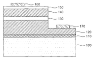
- FIG. 1 is a cross-sectional view of a typical nitride light emitting device.
- the nitride light emitting device includes a GaN buffer layer 110, an n-type clad layer 120, an active layer 130 having a single quantum well (SQW) structure of InGaN or a multi-quantum well (MQW) structure of InGaN, and p-type clad layer 140, which are sequentially stacked on a sapphire substrate 100 (i.e., light transmitting substrate).
- a portion of the p-type clad layer 140 and the active layer 130 is removed through mesa etching, such that the top portion of the n-type clad layer 120 is partially exposed.
- an n-type electrode 170 is formed on the exposed top portion of the n-type clad layer 120, and a transparent conductive layer 150 formed of ITO and a p-type electrode 160 are sequentially stacked on the p-type clad layer 140. Additionally, the GaN buffer layer 110 is generally formed with a thickness of several nm.
- a nitride semiconductor device typically includes a nitride semiconductor layer having a thickness of 5 ⁇ m or more on a heterogeneous substrate, substrate bow or warpage occurs severely. This makes it difficult to perform subsequent manufacturing processes such as substrate alignment, a photolithography process, and an etching process.
- the present disclosure provides a semiconductor substrate capable of preventing substrate bow or warpage and a method for manufacturing the same.
- the semiconductor substrate After a discontinuous hemispheric metal layer is formed on a substrate, the planarization of semiconductor layer is occurred by the deposition of semiconductor layer. Therefore, a plurality of voids is formed at the interface between the substrate and the semiconductor layer and a metal concentration gradient is formed on the semiconductor layer.
- the present disclosure also provides a semiconductor substrate capable of preventing substrate bow or warpage and a method for manufacturing the same.
- a semiconductor substrate capable of preventing substrate bow or warpage and a method for manufacturing the same.
- a nitride semiconductor layer is formed thereon for surface planarization. Therefore, a plurality of voids is formed at the interface between the substrate and the nitride semiconductor layer.
- the present disclosure also provides a semiconductor substrate and a method for manufacturing the same.
- the semiconductor substrate even if a device layer is relatively thickly formed while being applied to a subsequent manufacturing process for semiconductor device, substrate bow or warpage occurs less. Therefore, subsequent manufacturing processes for semiconductor device become easier and a product failure rate can be minimized.
- a semiconductor substrate includes: a substrate; a hemispheric metal layer formed on the substrate discontinuously; and a semiconductor layer formed on the hemispheric metal layer.
- the hemispheric metal layer may include Group III metal and the semiconductor layer may include nitride of the Group III metal.
- the Group III metal may include at least one of Ga and In.
- the semiconductor layer may include the plurality of voids formed at the interface between the substrate and the semiconductor layer.
- the semiconductor layer may have a concentration gradient in which the density of the metal is decreased in a thickness direction.
- a semiconductor substrate includes: a substrate; a hemispheric metal layer formed on the substrate discontinuously; and a semiconductor layer formed on the hemispheric metal layer, wherein the semiconductor layer has a concentration gradient in which metal density is decreased by the hemispheric metal layer in a thickness direction of the semiconductor layer; and the substrate has a final bow or warpage of less than 70 ⁇ m when the substrate has the size of 2 inches and the thickness of 430 ⁇ m and a total thickness of the hemispheric metal layer and the semiconductor layer is between 5 ⁇ m and 100 ⁇ m.
- the hemispheric metal layer may include Group III metal and the semiconductor layer includes nitride of the Group III metal.
- the Group III metal may include at least one of Ga and In.
- the semiconductor layer may include a plurality of voids formed at an interface between the substrate and the semiconductor layer.
- a method for manufacturing a semiconductor substrate including: preparing a substrate; forming a discontinuous hemispheric metal layer on the substrate; and forming a semiconductor layer on an entire structure including the hemispheric metal layer.
- the hemispheric metal layer may include Group III metal and the semiconductor layer includes nitride of the Group III metal.
- the Group III metal may include at least one of Ga and In.
- the forming of the hemispheric metal layer may be performed at a temperature of higher than a melting point of metal or lower than 450 °C.
- the forming of the hemispheric metal layer and the forming of the semiconductor layer may be repeatedly performed at least once.
- the method after at least one of the preparing of the substrate, the forming of the hemispheric metal layer, and the forming of the semiconductor layer, may further include at least one of: cleaning the surface of the substrate; and treating the surface of the substrate.
- the forming of the hemispheric metal layer and the forming of the semiconductor layer may be performed in different chambers.
- the forming of the hemispheric metal layer and the forming of the semiconductor layer may be performed in the same chamber.
- the semiconductor layer may include a plurality of voids formed at an interface between the substrate and the semiconductor layer.
- the semiconductor layer may have a concentration gradient in which density of the metal is decreased in a thickness direction of the semiconductor layer.
- a semiconductor substrate includes: a substrate; a hemispheric layer formed on the substrate discontinuously; and a nitride semiconductor layer formed on the hemispheric layer, wherein the hemispheric layer has a distribution of metal elements diffused from the substrate during a thermal treatment process.
- the substrate may include at least Al element, the Al element being diffused into the hemisphere layer.
- the hemispheric layer may have a concentration of Al element that is decreased as it goes far from an interface between the hemispheric layer and the substrate.
- the hemispheric layer may be formed of at least one metal selected from Ga, Al, and In.
- the hemispheric layer may be nitrided and the surface of the nitride semiconductor on the hemispheric layer may be planarized by the nitride semiconductor layer.
- the nitride semiconductor layer may include a plurality of voids at an interface between the substrate and the nitride semiconductor layer.
- a semiconductor substrate includes: a substrate: a hemispheric layer formed on the substrate discontinuously; and a nitride semiconductor layer formed on the hemispheric layer, wherein the hemispheric layer has a distribution of metal element diffused from the substrate during a thermal treatment process; and the metal elements have a concentration that is decreased as it goes far from the interface between the substrate and the hemispheric layer.
- the metal element may include Al element.
- the nitride semiconductor layer may include a plurality of voids formed at an interface between the substrate and the nitride semiconductor layer.
- the hemispheric layer may be nitrided and the surface of the nitride semiconductor on the hemispheric layer may be planarized by the nitride semiconductor layer.
- a method for manufacturing a semiconductor substrate includes: preparing a substrate; forming a hemispheric layer on the substrate discontinuously; performing a thermal treatment process such that a metal element in the substrate is diffused into the hemispheric layer; and forming a nitride semiconductor layer on the hemispheric layer.
- the metal element may include Al element.
- the hemispheric layer may be formed of at least one metal selected from Ga, Al, and In.
- the forming of the hemispheric metal layer may be performed at a temperature of higher than a melting point of metal used or a temperature of lower than 450 °C.
- the nitride semiconductor layer may be formed with more than a thickness that allows the surface of the nitride semiconductor on the hemispheric layer to be completely planarized.
- the forming of the hemispheric layer and the forming of the nitride semiconductor layer may be repeatedly performed at least once.
- the nitride semiconductor layer may include a plurality of voids at the interface between the substrate and the nitride semiconductor layer.
- a semiconductor layer is formed thereon for planarization. Therefore, a plurality of voids is formed at an interface between the substrate and the semiconductor layer, and a vertical metal concentration gradient is formed in the semiconductor layer. Additionally, the hemispheric metal layer remains at the interface therebetween. Accordingly, the voids in the semiconductor layer, the vertical metal concentration gradient of the semiconductor layer, and the remaining hemispheric metal layer are used for absorbing or relax the stain of interface. Thus, the substrate bow or warpage can be minimized.
- a nitride semiconductor layer is formed thereon for planarizing the surface of the nitride semiconductor on the hemispheric layer.
- a plurality of voids are formed at the interface between the substrate and the nitride semiconductor layer, and a discontinuous hemispheric layer including an element diffused from the substrate remains at the interface of the substrate. Accordingly, the voids and the remaining discontinuous hemispheric layer are used for absorbing or relaxing the strain of interface. Therefore, substrate bow or warpage can be minimized.
- the present invention even if a device layer is relatively thickly formed during a manufacturing process for the subsequent device, substrate bow or warpage occurs less. Therefore, substrate handling such as substrate chucking and substrate alignment becomes easier. Thus, the subsequent manufacturing processes such as a photolithography process and an etching process for the device can be performed without difficulties, and also a product failure rate can be minimized.
- FIG. 1 is a cross-sectional view of a typical nitride light emitting device
- FIG. 2 is a process flowchart illustrating a method for manufacturing a semiconductor substrate in accordance with one exemplary embodiment
- FIGS. 3 through 5 are cross-sectional views illustrating manufacturing processes of a semiconductor substrate in accordance with one exemplary embodiment
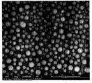
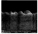
- FIGS. 6 and 7 are SEM photographs showing a plane view and a cross-sectional view of a hemispheric metal layer in accordance with one exemplary embodiment
- FIG. 8 is a graph illustrating bow or warpage characteristic of a semiconductor substrate in accordance with a first experimental example
- FIG. 9 is a graph illustrating bow or warpage characteristic in accordance with a first comparative example
- FIG. 10 is a process flowchart illustrating a method for manufacturing a semiconductor substrate in accordance with a first modification
- FIG. 11 is a process flowchart illustrating a method for manufacturing a semiconductor substrate in accordance with another exemplary embodiment
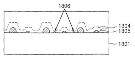
- FIGS. 12 through 15 are cross-sectional views illustrating manufacturing processes of a semiconductor substrate in accordance with another exemplary embodiment
- FIGS. 16 through 18 are SEM photographs and EDS analysis graphs of an AlxGa1-x hemispheric layer formed through a thermal treatment process in accordance with another embodiment
- FIG. 19 is a cross-sectional view illustrating a concentration gradient of an AlxGa1-x hemispheric layer formed through a thermal treatment process in accordance with another embodiment
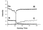
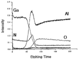
- FIGS. 20 and 21 are GDS analysis graphs of an AlxGa1-xN hemispheric layer in accordance with a second comparative example and second experimental example;
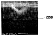
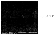
- FIGS. 22 and 23 are SEM photographs showing the cross-sectional view of a nitride semiconductor layer according to another exemplary embodiment.
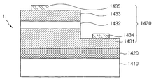
- FIG. 24 is a cross-sectional view illustrating a semiconductor device including a semiconductor substrate in accordance with a further another exemplary embodiment.
- a layer, a film, a region or a plate is referred to as being ‘between’ two layers, films, regions or plates, it can be the only layer, film, region or plate between the two layers, films, regions or plates, or one or more intervening layers, films, regions or plates may also be present.
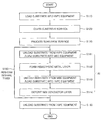
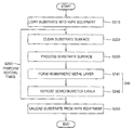
- FIG. 2 is a process flowchart illustrating a method for manufacturing a semiconductor substrate in accordance with one exemplary embodiment.
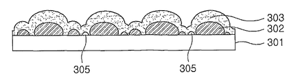
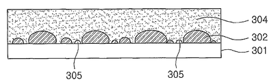
- FIGS. 3 through 5 are cross-sectional views illustrating manufacturing processes of a semiconductor substrate in accordance with one exemplary embodiment.
- a prepared chamber is purged using N2 gas, a substrate is loaded into the chamber and mounted on a substrate holder in the chamber.
- the substrate holder may be any means that can stably fix the substrate at a deposition position.
- the substrate holder may be a holder type that holds a substrate surface vertically or a stage type that holds the substrate surface horizontally.
- the substrate may be a Silicon On Insulation (SOI) substrate having a single crystal semiconductor layer or be a single crystal semiconductor wafer.
- the single crystal semiconductor layer may be one of a single crystal silicon layer, a single crystal sapphire layer, a single crystal germanium layer, a single crystal silicon germanium layer, and a single crystal silicon carbide layer.
- the single crystal semiconductor wafer may be one of a single crystal silicon wafer, a single crystal sapphire wafer, a single crystal germanium wafer, a single crystal silicon germanium wafer, and a single crystal silicon carbide wafer.
- the single crystal sapphire wafer (hereinafter, referred to as a sapphire substrate) will be used exemplarily.
- impurities remaining on the substrate surface are removed by using a cleaning gas, for example.
- the surface cleaning is performed for about 5 min to about 30 min by using a mixture gas of HCl and N2 having a mixing ratio of about 1:5 to 1:10.
- nitrogen (N)-containing gas and/or oxygen-containing gas is/are supplied to form at least one thin layer of a nitride layer, an oxide layer, and oxy-nitride layer.
- N-containing reaction such as N2, NH3, and NH3/N2
- a nitride layer is formed
- an N and O-containing reaction gas such as a mixture gas of NH3 and O2
- an oxy-nitride layer is formed.
- an N, O and Si-containing reaction gas such as a mixture gas of N2O and Si is supplied, a silicon oxy-nitride layer is formed.
- Operations S120 for cleaning the surface and S130 for treating the surface may be simultaneously performed and any one of them can be omitted. Additionally, operations S120 and S130 may be performed using a Hydride Vapor Phase Epitaxy (HVPE) process.
- HVPE Hydride Vapor Phase Epitaxy
- the HVPE process provides source-reaction gas and carrier gas to a container, which is connected to the inside of the chamber and in which source material is supplied (for example, a supply tube in which a metal source material is supplied), to allow the source gas dissolved from the source material and the reaction gas is individually supplied through individual gas line to be applied to the heated substrate surface in the chamber.
- source material for example, a supply tube in which a metal source material is supplied
- the reaction gas is individually supplied through individual gas line to be applied to the heated substrate surface in the chamber.
- the vapor reaction with the source gas and reaction gas occurs, so that the product of the vapor reaction is deposited on the heated substrate surface in the chamber to grow a desired thin layer on the substrate.
- the source-reaction gas may be HCl gas and the reaction gas may be NH3.
- the carrier gas may be an inert gas such as N2 and Ar.
- Operation S140 for forming a semiconductor layer with a discontinuous hemispheric metal layer includes operation S142 for forming a discontinuous hemispheric metal layer using Group III metal by the supplying of the source gas without the supplying of the reaction gas on the surface treated substrate and operation S144 for forming a nitride semiconductor layer in a single layer or a multi layer structure on the hemispheric metal layer by the supplying of both the source gas and the reaction gas .
- Ga metal is deposited on the surface treated substrate 301 at a temperature of higher than a melting point of the Ga metal or lower than 450 °C through various methods such as sputtering, Molecular Beam Epitaxy (MBE), E-Beam evaporator, Metal Organic Chemical Vapor Deposition (MOCVD), and HVPE.
- MBE Molecular Beam Epitaxy
- MOCVD Metal Organic Chemical Vapor Deposition
- HVPE High vacuum chemical vapor deposition
- the hemispheric metal layer 302 may be formed with the size of about 0.1 ⁇ m to 5 ⁇ m over an entire area of the substrate 301.
- the hemispheric metal layer 302 is not limited to the Ga metal, and may be formed of Group III metal, for example, In metal.
- a nitride semiconductor layer 303 when a nitride semiconductor layer 303 is deposited on an entire structure including the hemispheric metal layer 302, the nitride semiconductor layer 303 grows vertically and horizontally from the surface of the hemispheric metal layer 302. Accordingly, a void 305 is formed between the hemispheric metal layer 302, and a space between the hemispheric metal layers 302 becomes smaller. Also, when the nitride semiconductor layer 303 is deposited with a sufficient thickness as shown in FIG. 5, the space between the hemispheric metal layers 302 is filled and thus the top surface of the nitride semiconductor layer 303 is planarized appropriate for the growth of subsequent layers for the device.
- the nitride semiconductor layer 303 may be formed with a thickness of about 5 ⁇ m to 100 ⁇ m through various methods such as MBE, MOCVD, and HVPE.
- the hemispheric metal layer 302 and the nitride semiconductor layer 303 are separately formed, but can be formed almost simultaneously.
- the nitride semiconductor layer 303 may be formed in a multi layer not a single layer.
- operation S142 for forming the hemispheric metal layer may be performed through manufacturing equipment different from those of operations S130 and S144. That is, after the preceding operation S130 for treating the substrate surface is completed, the substrate may be unloaded from HVPE equipment and then loaded into MBE equipment to form a hemispheric metal layer on the substrate. Next, the substrate may be unloaded from the MBE equipment again, and then loaded into the HVPE equipment to perform the following operation S144 for forming a nitride semiconductor layer.
- operation S142 or S144 may be repeatedly performed at least once, and all operations S142 and S144 may be repeatedly performed at least once. Additionally, in operation S140, at least one of operation S120 for cleaning the surface and operation S130 for treating the surface may be selectively performed. For example, operation S120 for cleaning the surface may be previously performed before operation S142 or S144, and then operation S130 for treating the surface may be performed. Or, if necessary for manufacturing processes, operation S120 for cleaning the surface or operation S130 for treating the surface may be performed independently.
- operation S160 for unloading the substrate after operations S110 to S130 are completed, purging is performed using N2 gas. While the purging is continuously performed using the N2 gas, temperature is slowly decreased until the internal temperature of the chamber reaches the room temperature. Through this, thermal impact on the substrate can be minimized.
- the substrate is dismounted from the substrate holder and the dismounted substrate is drawn into the external of the chamber. At this point, the drawn substrate may be placed for the next process for forming a device layer of an electronic device such as a power device, a light emitting device, and a light receiving device on the substrate.
- a semiconductor layer including a discontinuous hemispheric metal layer with the thickness of approximately 15 ⁇ m on the substrate is formed. Therefore, a semiconductor substrate with less bow or warpage can be manufactured, and its characteristics will be described below.
- FIGS. 6 and 7 are Scanning Electron Microscope (SEM) photographs showing a plane view and a cross-sectional view of a hemispheric metal layer in accordance with one exemplary embodiment.
- the hemispheric metal layer is formed using Ga metal through a MBE method under a temperature condition of 200 °C. Referring to FIGS. 6 and 7, it is confirmed that the hemispheric metal layer has a size of approximately 0.1 ⁇ m to 2 ⁇ m. Additionally, it is confirmed that the hemispheric metal layer has a three-dimensional structure.
- a nitride semiconductor layer formed on the hemispheric metal layer has a three-dimensional structure also. Due to this, a plurality of voids is formed in the nitride semiconductor layer, thereby relaxing the stain of interface between the nitride semiconductor layer and the substrate. Additionally, since the hemispheric metal layer supplies Ga metal to the nitride semiconductor layer during the forming of the nitride semiconductor layer, a vertical concentration gradient of the Ga metal is formed in the nitride semiconductor layer according to the height.
- the vertical concentration gradient of the Ga metal serves to relax the strain of interface between the substrate and the nitride semiconductor layer, and also the Ga metal remaining on the substrate serves to relax the strain of interface between the substrate and the nitride semiconductor layer. As a result, a semiconductor substrate having relatively less bow or warpage can be manufactured.
- FIG. 8 is a graph illustrating bow or warpage characteristic of a semiconductor substrate in accordance with a first experimental example.
- FIG. 9 is a graph illustrating bow or warpage characteristic in accordance with a first comparative example.
- a hemispheric metal layer of Ga metal is formed on a sapphire substrate, with a size of approximately 0.1 ⁇ m to 2 ⁇ m through an MEB method, and a nitride semiconductor layer is formed with a thickness of 3 ⁇ m through an HVPE method.
- bow or warpage of 7.25 ⁇ m occurs under the conditions where the sapphire substrate has the thickness of 430 ⁇ m and its size is 1 inch. If this is converted into the substrate conditions where the sapphire substrate has the thickness of 430 ⁇ m and its size is 2 inches, bow or warpage is calculated between 28 ⁇ m and 30 ⁇ m.
- a nitride semiconductor layer having the thickness of 2 ⁇ m is formed on the sapphire substrate under the same condition except for the hemispheric metal layer.
- bow or warpage of 18.01 ⁇ m occurs under the conditions where the sapphire substrate has the thickness of 430 ⁇ m and its size is 1 inch. If this is converted into the substrate conditions where the sapphire substrate has the thickness of 430 ⁇ m and its size is 2 inches, bow or warpage is calculated between 72 ⁇ m to 75 ⁇ m. It is confirmed that through the comparison, the semiconductor substrate of the embodiment has less bow or warpage.
- a plurality of voids in the nitride semiconductor layer including the discontinuous hemispheric metal layer, a concentration gradient of the Ga metal, and the remaining Ga metal alleviate interface stress between the substrate and the nitride semiconductor layer.
- FIG. 10 is a process flowchart illustrating a method for manufacturing a semiconductor substrate in accordance with a first modification.
- all processes may be performed in the single process equipment.
- HVPE equipment in which one or a plurality of gas lines is/are connected to one chamber such that it is possible to supply various gases
- operation S210 for cleaning the substrate surface, operation S220 for treating the substrate surface, operation S241 for forming a discontinuous hemispheric metal layer, and operation S242 for forming a nitride semiconductor layer can be performed continuously. Accordingly, manufacturing time increase and substrate contamination do not occur while the substrate transfers to a plurality of chambers.
- FIG. 11 is a process flowchart illustrating a method for manufacturing a semiconductor substrate in accordance with another exemplary embodiment.
- FIGS. 12 through 15 are cross-sectional views illustrating manufacturing processes of a semiconductor substrate in accordance with another exemplary embodiment.
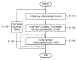
- the method for manufacturing a semiconductor substrate includes operation S1110 for forming a discontinuous hemispheric layer on a substrate, operation S1120 for performing a thermal treatment process on the substrate and the hemispheric layer, and operation S1130 for forming a nitride semiconductor layer on the thermally-treated hemispheric layer.
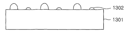
- a discontinuous hemispheric layer 1302 is formed on a predetermined substrate 1301.
- the substrate 1301 includes at least Al element.
- this embodiment uses the sapphire substrate 1301 having a chemical formula of Al2O3.
- the hemispheric layer 1302 may be formed of at least one metal selected from Group III elements such as Ga, Al, and In.
- this embodiment uses Ga metal.
- the Ga metal is deposited on the sapphire substrate 1301 at a temperature of higher than a melting point of the Ga metal or lower than 450 °C through various methods such as sputtering, MBE, E-Beam evaporator, MOCVD, CVD and HVPE.
- sputtering MBE, E-Beam evaporator, MOCVD, CVD and HVPE.
- MOCVD molyzed chemical vapor deposition
- HVPE high vacuum chemical vapor deposition
- hemispheres having a size of approximately 0.1 ⁇ m to 5 ⁇ m are discontinuously formed on the sapphire substrate 1301 to form a Ga hemispheric layer 1302.
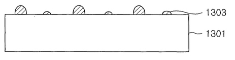
- a thermal treatment process is performed on the sapphire substrate 1301 having the Ga hemispheric layer thereon in operation S1120. Accordingly, Al element of the sapphire substrate 1301 is diffused into the hemispheric layer 1302 such that the initial Ga hemispheric layer 1302 is changes into an AlxGa1-x hemispheric layer containing Al element.
- This AlxGa1-x hemispheric layer 1303 may function as a seed that facilitate the growth of a nitride semiconductor layer that will be formed later.
- the AlxGa1-x hemispheric layer 1303 includes a plurality of discontinuously formed hemispheres, and each hemisphere may be formed with a preferable size of approximately 0.1 ⁇ m to 5 ⁇ m over entire areas of the substrate 1301.
- Operation S1120 for performing the thermal treatment may be performed for approximately 1 min to 60 min at a temperature between approximately 700 °C to 1100 °C through equipment that will be used in operation S1130 for forming the a nitride semiconductor layer (that is, the next operation)
- a nitride semiconductor layer 1304 is deposited on the entire structure including the AlxGa1-x hemispheric layer 1303 to planarize the surface of the AlxGa1-x hemispheric layer 1303 in operation S1130. Accordingly, the AlxGa1-x hemispheric layer 1303 is nitrided into an AlxGa1-xN hemispheric layer 1305 and thus, voids 1306 are formed therein. Therefore, space between the AlxGa1-xN hemispheric layer 1305 becomes gradually narrower. As illustrated in FIG.
- the nitride semiconductor layer 1304 may be formed with a thickness of approximately 5 ⁇ m to 100 ⁇ m through various methods such as MBE, MOCVD, and HVPE.
- the AlxGa1-x hemispheric layer 1303 and the nitride semiconductor layer 1304 are repeatedly formed in operation S1140 to form a predetermined thickness on the substrate 1301.
- the AlxGa1-x hemispheric layer 1303 and the nitride semiconductor layer 1304 may not be repeatedly formed and any one of the AlxGa1-x hemispheric layer 1303 and the nitride semiconductor layer 1304 can be selectively repeatedly formed.
- an AlxGa1-xN hemispheric layer (which is nitrided from the AlxGa1-x hemispheric layer)/a first nitride semiconductor layer/a second nitride semiconductor layer are formed on the substrate 1301 in order to form only the nitride semiconductor layer having a multi-layer structure in operation S1150.
- the semiconductor substrate manufactured through the above manufacturing processes can be used as a substrate for forming a device layer thereon, which is an electronic device such as a power device, a light emitting device, and a light receiving device.
- a nitride semiconductor layer including a discontinuous AlxGa1-xN hemispheric layer 1305 is formed with the thickness of approximately 5 ⁇ m to 15 ⁇ m on the semiconductor substrate manufactured through the above processes.
- This nitride semiconductor layer absorbs or relaxes the strain of interface between the nitride semiconductor layer and a device layer that will be formed later. That is, during the forming of the next layer, bow or warpage occurs less such that the subsequent process can be performed without difficulties.
- characteristics of the hemispheric layer 1303 or 1305 formed on the semiconductor substrate and its bow or warpage characteristics will be described in more detail below.
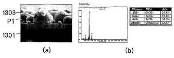
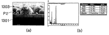
- FIGS. 16 through 18 are a SEM cross-sectional picture ((a) of each figure) and an Energy Dispersive X-ray Spectroscopy (EDS) analysis graph ((b) of each figure) of an AlxGa1-x hemispheric layer formed through a thermal treatment process in accordance with another embodiment.
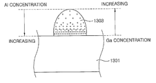
- FIG. 19 is a cross-sectional view illustrating a concentration gradient of an AlxGa1-x hemispheric layer formed through a thermal treatment process in accordance with another embodiment.
- P1, P2, and P3 of the SEM cross-sectional picture represent points where EDS analysis is performed.
- Al element is distributed in the inside P1 and P2 of the AlxGa1-x hemispheric layer 1303, and Al element content is increased as it approaches the surface of the sapphire substrate 1301 (P1 -> P2). Additionally, Ga element is not distributed in the inside P3 of the sapphire substrate 1301. Ga element is penetrated near the interface of the Ga hemispheric layer and the sapphire substrate. Referring to FIG. 19 where the experimental results are summarized, concentration of Al element in the AlxGa1-x hemisphere layer 1303 is increased as it approaches the interface of the sapphire substrate 1301, and concentration of Ga element is increased as it goes far from the surface of the sapphire substrate 1301.
- Ga element of the hemispheric layer 1303 does not diffuse into the inside of the sapphire substrate 1301 and penetrate restrictively through the surface of the sapphire substrate.
- a discontinuous Ga hemispheric layer which is formed first on the substrate 1301, is thermally heated to form the discontinuous AlxGa1-x hemispheric layer 1303 having Al element of which concentration gradient is decreased as it goes far from the surface of the substrate 1301.
- FIGS. 20 and 21 are Glow Discharge Spectrometry (GDS) analysis graphs of an AlxGa1-xN hemispheric layer in accordance with a second comparative example and second experimental example.
- GDS Glow Discharge Spectrometry
- FIG. 20 a GaN layer of 5 ⁇ m is formed on a sapphire substrate through MOCVD equipment as a second comparative example.
- FIG. 21 a GaN layer of 5 ⁇ m is formed on a sapphire substrate through MOCVD equipment as a second experimental example.
- Al and N elements are more distributed at the interface between the sapphire substrate and the GaN layer in the second experimental example of FIG. 19.
- the initial AlxGa1-x hemispheric layer is changed into AlxGa1-xN hemispheric layer. That is, during the forming of the GaN layer, the initial AlxGa1-x hemispheric layer is changed into the AlxGa1-xN hemispheric layer. And, this layer alleviates the strain of the interface between the substrate and the GaN layer.
- FIGS. 22 and 23 are SEM cross-sectional pictures of a nitride semiconductor layer according to another exemplary embodiment.
- a thermal treatment process is performed for 5 min at a temperature of 900 °C through a MOCVD method
- a GaN layer is formed with the thickness of 3 ⁇ m through a MOCVD method.
- a thermal treatment process is performed for 5 min at a temperature of 1050 °C through a HVPE method
- a GaN layer is formed with the thickness of 20 ⁇ m through a HVPE method.
- a thin layer growth of the GaN layer is controlled by a three-dimensional structure of a discontinuous AlxGa1-x hemispheric layer disposed below the GaN layer, thereby providing three-dimensional thin layer characteristics. Due to this, a plurality of voids is formed in the GaN layer, and also can relax the strain of interface between a device layer (which will be formed later) and the substrate. Additionally, as mentioned above, the initial AlxGa1-x hemispheric layer is changed into the AlxGa1-xN hemispheric layer during the forming of the GaN layer, thereby alleviate the interface stress between the substrate and the GaN layer. As a result, a semiconductor substrate, where bow or warpage occurs relatively less, can be manufactured.
- a discontinuous Ga hemispheric layer is formed on a sapphire substrate, with a size of 0.1 ⁇ m to y 5 ⁇ m through an E-beam evaporator method. Then, a thermal treatment process is performed through MOCVD equipment to form a discontinuous AlxGa1-x hemispheric layer. Additionally, a nitride semiconductor layer is formed with the thickness of 3 ⁇ m through the MOCVD equipment. In this case, bow or warpage of 17.81 ⁇ m is measured under the conditions where the sapphire substrate has the thickness of 430 ⁇ m and the size of 2 inches.
- a nitride semiconductor layer is formed with a thickness of 3 ⁇ m on the sapphire substrate under the same condition except for the discontinuous AlxGa1-x hemispheric layer.
- bow or warpage of 32.02 ⁇ m is measured under the conditions where the sapphire substrate has the thickness of 430 ⁇ m and the size of 2 inches.
- FIG. 24 is a cross-sectional view illustrating a semiconductor device including a semiconductor substrate in accordance with a further another exemplary embodiment.
- the semiconductor device includes a substrate 1410, a nitride semiconductor layer 1420 including a discontinuous hemisphere layer on the substrate 1410, and the electronic device layer 1430 on the nitride semiconductor layer 1420.
- This semiconductor device includes at least one light emitting device L that converts electric energy into light energy, thereby it can be used in a light source module.
- the substrate 1410 may uses a SOI substrate including a single crystal semiconductor layer or a single crystal semiconductor wafer.
- this embodiment uses a sapphire substrate.
- the nitride semiconductor layer 1420 is formed by planarizing the surface.
- Group III metal is used to form a discontinuous hemispheric metal layer with a size of approximately 0.1 ⁇ m to 5 ⁇ m, on the surface treated substrate 1410, and a nitride semiconductor layer of a single layer or a multi layer is formed with the thickness of 5 ⁇ m on an entire structure including the discontinuous hemispheric metal layer, in order to form the nitride semiconductor layer 1420 including the discontinuous hemispheric metal layer.
- a plurality of voids is formed in the nitride semiconductor layer 1420 including the discontinuous hemispheric metal layer.
- a concentration gradient of the Ga metal in the hemispheric metal layer and the remaining Ga metal relax the strain of interface between the substrate 1410 and the nitride semiconductor layer, such that bow or warpage of the substrate 1410 occurs less.
- a discontinuous Ga hemispheric layer is formed with a size of approximately 0.1 ⁇ m to 5 ⁇ m, on the substrate 1410. Then, through the thermal treatment process, the discontinuous AlxGa1-x hemispheric layer is formed with a size of approximately 0.1 ⁇ m to 5 ⁇ m.
- a nitride semiconductor layer of a single layer or a multi layer is formed on an entire structure including the discontinuous AlxGa1-x hemispheric layer.
- the AlxGa1-x hemispheric layer is nitrided into an AlxGa1-xN hemispheric layer.
- a plurality of voids is formed in the nitride semiconductor layer 1420 including the discontinuous AlxGa1-xN hemispheric layer. Additionally, the discontinuous AlxGa1-xN hemispheric layer relax the strain of interface between the substrate 1410 and a nitride semiconductor layer (which will be formed later), such that bow or warpage of the substrate 1410 occurs less.
- At least one light emitting device L is provided in the electronic device layer 1430.
- the light emitting device L includes a semiconductor layer.
- the semiconductor layer includes an n-type layer 1431, an active layer 1432, and a p-type layer 1433, a first electrode 1434 that is formed on a top portion of the n-type layer 1431, and a second electrode 1435 that is formed on a top portion of the p-type layer 1433, which are stacked on the nitride semiconductor layer 1420 including a discontinuous semi metal layer of the substrate 1410.
- the n-type layer 1431, the active layer 1432, and the p-type layer 1433 may be formed of a semiconductor thin layer including at least one of Si, GaN, AlN, InGaN, AlGaN, and AlInGaN.
- the n-type layer 1431 and the p-type layer 1433 are formed of a GaN thin layer, and the active layer 1432 is formed of an InGaN thin layer.
- the n-type layer 1431 provides electrons and may be formed by implanting an n-type dopant such as Si, Ge, Se, Te, and C into the above-mentioned semiconductor layer.
- the p-type layer 1433 provides holes and may be formed by implanting a p-type dopant such as Mg, Zn, Be, Ca, Sr, and Ba into the above-mentioned semiconductor layer.
- the active layer 1432 is a layer for outputting light of a predetermined wavelength when electrons from the n-type layer 1431 and holes from the p-type layer 1433 are combined.
- the active layer 1432 may be formed of a multi-layered semiconductor thin layer having a single quantum well structure or a multiple quantum well structure, which is formed by stacking a well layer and a barrier layer alternately. According to a semiconductor material constituting the active layer 1432, a wavelength of an outputted light varies. Therefore, an appropriate semiconductor material needs to be selected according to a targeted output wavelength.
- the nitride semiconductor layer 1420 including a discontinuous hemispheric metal layer or a discontinuous AlxGa1-xN hemispheric layer absorb and relax the strain between the substrate 1410 and the electronic device layer 1430, bow or warpage of the substrate 1410 occurs less during the forming of the electronic device layer 1430 on the substrate 1410. Accordingly, since handling of the substrate such as substrate chucking, substrate alignment may be completed without difficulties during the subsequent processes, typical disadvantages such as decrease about product yield and life time can be prevented.
- a nitride semiconductor layer including a discontinuous hemispheric metal layer or a discontinuous AlxGa1-xN hemispheric layer is formed on a substrate and a light emitting device L is formed on the substrate.
- the present invention is not limited thereto. That is, various devices (such as a transistor, a photovoltaic cell, a Metal-Oxide Semiconductor Field Effect Transistor (MOSFET), the Schottky diode, and a photo sensor) can be formed on the substrate.
- MOSFET Metal-Oxide Semiconductor Field Effect Transistor
Landscapes
- Recrystallisation Techniques (AREA)
- Led Devices (AREA)
- Electrodes Of Semiconductors (AREA)
Abstract
L'invention concerne un substrat de semi-conducteur et son procédé de fabrication. Le substrat de semi-conducteur inclut un substrat, une couche métallique discontinue formée de particules hémisphériques sur le substrat et une couche de semi-conducteur située sur la couche métallique de particules hémisphériques. Une pluralité de vides, sur l'interface du substrat et de la couche discontinue de particules hémisphériques, permet d'absorber ou de relaxer les contraintes au niveau de l'interface. En conséquence, même si une couche relativement épaisse est ultérieurement formée sur le substrat, toute courbure ou déformation est minimisée.
Priority Applications (1)
| Application Number | Priority Date | Filing Date | Title |
|---|---|---|---|
| US12/935,978 US8729670B2 (en) | 2008-04-16 | 2009-04-15 | Semiconductor substrate and method for manufacturing the same |
Applications Claiming Priority (4)
| Application Number | Priority Date | Filing Date | Title |
|---|---|---|---|
| KR10-2008-0035114 | 2008-04-16 | ||
| KR1020080035114A KR100990971B1 (ko) | 2008-04-16 | 2008-04-16 | 반도체 기판과 이의 제조 방법 |
| KR1020080104550A KR101018760B1 (ko) | 2008-10-24 | 2008-10-24 | 반도체 기판과 이의 제조 방법 |
| KR10-2008-0104550 | 2008-10-24 |
Publications (3)
| Publication Number | Publication Date |
|---|---|
| WO2009128646A2 true WO2009128646A2 (fr) | 2009-10-22 |
| WO2009128646A3 WO2009128646A3 (fr) | 2010-01-07 |
| WO2009128646A9 WO2009128646A9 (fr) | 2011-01-27 |
Family
ID=41199567
Family Applications (1)
| Application Number | Title | Priority Date | Filing Date |
|---|---|---|---|
| PCT/KR2009/001932 Ceased WO2009128646A2 (fr) | 2008-04-16 | 2009-04-15 | Substrat de semi-conducteur et son procédé de fabrication |
Country Status (2)
| Country | Link |
|---|---|
| US (1) | US8729670B2 (fr) |
| WO (1) | WO2009128646A2 (fr) |
Cited By (1)
| Publication number | Priority date | Publication date | Assignee | Title |
|---|---|---|---|---|
| EP3176293A4 (fr) * | 2014-08-29 | 2018-07-04 | Soko Kagaku Co., Ltd. | Gabarit pour croissance épitaxiale et son procédé de fabrication, et dispositif semi-conducteur au nitrure |
Families Citing this family (2)
| Publication number | Priority date | Publication date | Assignee | Title |
|---|---|---|---|---|
| CN113410351B (zh) * | 2021-06-17 | 2022-11-08 | 錼创显示科技股份有限公司 | 磊晶半导体结构与磊晶基板 |
| TWI777621B (zh) | 2021-06-17 | 2022-09-11 | 錼創顯示科技股份有限公司 | 磊晶半導體結構與磊晶基板 |
Family Cites Families (5)
| Publication number | Priority date | Publication date | Assignee | Title |
|---|---|---|---|---|
| GB0111207D0 (en) * | 2001-05-08 | 2001-06-27 | Btg Int Ltd | A method to produce germanium layers |
| KR100744933B1 (ko) * | 2003-10-13 | 2007-08-01 | 삼성전기주식회사 | 실리콘 기판 상에 형성된 질화물 반도체 및 그 제조 방법 |
| KR100682872B1 (ko) | 2004-12-08 | 2007-02-15 | 삼성전기주식회사 | 고효율 반도체 발광 소자 및 그 제조방법 |
| WO2008048303A2 (fr) * | 2005-12-12 | 2008-04-24 | Kyma Technologies, Inc. | Articles en nitrures du groupe III et leurs procédés de fabrication |
| KR100867518B1 (ko) * | 2006-09-06 | 2008-11-07 | 삼성전기주식회사 | 질화물계 반도체 발광소자의 제조방법 |
-
2009
- 2009-04-15 WO PCT/KR2009/001932 patent/WO2009128646A2/fr not_active Ceased
- 2009-04-15 US US12/935,978 patent/US8729670B2/en not_active Expired - Fee Related
Cited By (1)
| Publication number | Priority date | Publication date | Assignee | Title |
|---|---|---|---|---|
| EP3176293A4 (fr) * | 2014-08-29 | 2018-07-04 | Soko Kagaku Co., Ltd. | Gabarit pour croissance épitaxiale et son procédé de fabrication, et dispositif semi-conducteur au nitrure |
Also Published As
| Publication number | Publication date |
|---|---|
| WO2009128646A3 (fr) | 2010-01-07 |
| WO2009128646A9 (fr) | 2011-01-27 |
| US8729670B2 (en) | 2014-05-20 |
| US20110024878A1 (en) | 2011-02-03 |
Similar Documents
| Publication | Publication Date | Title |
|---|---|---|
| CN109950372B (zh) | 发光二极管外延片及其制造方法 | |
| US20120070929A1 (en) | Method for fabricating wafer product and method for fabricating gallium nitride based semiconductor optical device | |
| WO2013018937A1 (fr) | Dispositif électroluminescent à semi-conducteurs | |
| WO2011046292A2 (fr) | Dispositif à semi-conducteur non polaire ou semi-polaire de grande qualité sur un semi-conducteur nitrure poreux, et procédé pour sa fabrication | |
| WO2013022227A2 (fr) | Élément électroluminescent semi-conducteur au nitrure donnant un meilleur étalement d'intensité de courant et son procédé de fabrication | |
| WO2014168339A1 (fr) | Dispositif d'émission de lumière ultraviolette | |
| WO2010055987A1 (fr) | Procédé de fabrication de substrat d'oxyde de gallium, dispositif électroluminescent et son procédé de fabrication | |
| WO2009119498A1 (fr) | Élément électroluminescent à semi-conducteur au nitrure | |
| EP2389693A2 (fr) | Dispositif à semi-conducteurs, dispositif électroluminescent et leur procédé de fabrication | |
| WO2021158016A1 (fr) | Diode électroluminescente multi-bande à puce unique | |
| CN114927601B (zh) | 一种发光二极管及其制备方法 | |
| WO2016108423A1 (fr) | Dispositif électroluminescent | |
| JP3603598B2 (ja) | 3−5族化合物半導体の製造方法 | |
| JP2004134750A (ja) | p型III族窒化物系化合物半導体の製造方法 | |
| WO2009093846A2 (fr) | Procédé de fabrication d'un dispositif électroluminescent | |
| WO2010147357A4 (fr) | Substrat hétérogène, dispositif à semi-conducteurs à base de nitrure l'utilisant et son procédé de fabrication | |
| US8470697B2 (en) | Method of forming p-type compound semiconductor layer | |
| US8729670B2 (en) | Semiconductor substrate and method for manufacturing the same | |
| WO2022240179A1 (fr) | Diode électroluminescente multibande | |
| WO2016159614A1 (fr) | Dispositif émetteur de lumière uv | |
| CN109686821B (zh) | 一种发光二极管的外延片的制备方法 | |
| KR19990023288A (ko) | 3-5족 화합물 반도체의 제조방법 | |
| CN115084329B (zh) | 一种应用于Si衬底上的LED外延片及其生长方法 | |
| JP5020667B2 (ja) | 発光デバイス | |
| WO2023003446A1 (fr) | Procédé de fabrication d'un dispositif électroluminescent à semi-conducteur au nitrure du groupe iii |
Legal Events
| Date | Code | Title | Description |
|---|---|---|---|
| 121 | Ep: the epo has been informed by wipo that ep was designated in this application |
Ref document number: 09732727 Country of ref document: EP Kind code of ref document: A2 |
|
| WWE | Wipo information: entry into national phase |
Ref document number: 12935978 Country of ref document: US |
|
| NENP | Non-entry into the national phase |
Ref country code: DE |
|
| 122 | Ep: pct application non-entry in european phase |
Ref document number: 09732727 Country of ref document: EP Kind code of ref document: A2 |