WO2009133897A1 - 接続材料及び半導体装置 - Google Patents
接続材料及び半導体装置 Download PDFInfo
- Publication number
- WO2009133897A1 WO2009133897A1 PCT/JP2009/058375 JP2009058375W WO2009133897A1 WO 2009133897 A1 WO2009133897 A1 WO 2009133897A1 JP 2009058375 W JP2009058375 W JP 2009058375W WO 2009133897 A1 WO2009133897 A1 WO 2009133897A1
- Authority
- WO
- WIPO (PCT)
- Prior art keywords
- metal particles
- connection material
- weight
- methacrylate
- acrylate
- Prior art date
- Legal status (The legal status is an assumption and is not a legal conclusion. Google has not performed a legal analysis and makes no representation as to the accuracy of the status listed.)
- Ceased
Links
Images




Classifications
-
- H—ELECTRICITY
- H05—ELECTRIC TECHNIQUES NOT OTHERWISE PROVIDED FOR
- H05K—PRINTED CIRCUITS; CASINGS OR CONSTRUCTIONAL DETAILS OF ELECTRIC APPARATUS; MANUFACTURE OF ASSEMBLAGES OF ELECTRICAL COMPONENTS
- H05K3/00—Apparatus or processes for manufacturing printed circuits
- H05K3/30—Assembling printed circuits with electric components, e.g. with resistors
- H05K3/32—Assembling printed circuits with electric components, e.g. with resistors electrically connecting electric components or wires to printed circuits
- H05K3/321—Assembling printed circuits with electric components, e.g. with resistors electrically connecting electric components or wires to printed circuits by conductive adhesives
-
- C—CHEMISTRY; METALLURGY
- C09—DYES; PAINTS; POLISHES; NATURAL RESINS; ADHESIVES; COMPOSITIONS NOT OTHERWISE PROVIDED FOR; APPLICATIONS OF MATERIALS NOT OTHERWISE PROVIDED FOR
- C09J—ADHESIVES; NON-MECHANICAL ASPECTS OF ADHESIVE PROCESSES IN GENERAL; ADHESIVE PROCESSES NOT PROVIDED FOR ELSEWHERE; USE OF MATERIALS AS ADHESIVES
- C09J11/00—Features of adhesives not provided for in group C09J9/00, e.g. additives
- C09J11/02—Non-macromolecular additives
- C09J11/04—Non-macromolecular additives inorganic
-
- C—CHEMISTRY; METALLURGY
- C09—DYES; PAINTS; POLISHES; NATURAL RESINS; ADHESIVES; COMPOSITIONS NOT OTHERWISE PROVIDED FOR; APPLICATIONS OF MATERIALS NOT OTHERWISE PROVIDED FOR
- C09J—ADHESIVES; NON-MECHANICAL ASPECTS OF ADHESIVE PROCESSES IN GENERAL; ADHESIVE PROCESSES NOT PROVIDED FOR ELSEWHERE; USE OF MATERIALS AS ADHESIVES
- C09J9/00—Adhesives characterised by their physical nature or the effects produced, e.g. glue sticks
- C09J9/02—Electrically-conducting adhesives
-
- H—ELECTRICITY
- H10—SEMICONDUCTOR DEVICES; ELECTRIC SOLID-STATE DEVICES NOT OTHERWISE PROVIDED FOR
- H10W—GENERIC PACKAGES, INTERCONNECTIONS, CONNECTORS OR OTHER CONSTRUCTIONAL DETAILS OF DEVICES COVERED BY CLASS H10
- H10W70/00—Package substrates; Interposers; Redistribution layers [RDL]
- H10W70/40—Leadframes
- H10W70/411—Chip-supporting parts, e.g. die pads
- H10W70/417—Bonding materials between chips and die pads
-
- H—ELECTRICITY
- H10—SEMICONDUCTOR DEVICES; ELECTRIC SOLID-STATE DEVICES NOT OTHERWISE PROVIDED FOR
- H10W—GENERIC PACKAGES, INTERCONNECTIONS, CONNECTORS OR OTHER CONSTRUCTIONAL DETAILS OF DEVICES COVERED BY CLASS H10
- H10W74/00—Encapsulations, e.g. protective coatings
- H10W74/40—Encapsulations, e.g. protective coatings characterised by their materials
- H10W74/47—Encapsulations, e.g. protective coatings characterised by their materials comprising organic materials, e.g. plastics or resins
- H10W74/473—Encapsulations, e.g. protective coatings characterised by their materials comprising organic materials, e.g. plastics or resins containing a filler
-
- C—CHEMISTRY; METALLURGY
- C08—ORGANIC MACROMOLECULAR COMPOUNDS; THEIR PREPARATION OR CHEMICAL WORKING-UP; COMPOSITIONS BASED THEREON
- C08K—Use of inorganic or non-macromolecular organic substances as compounding ingredients
- C08K3/00—Use of inorganic substances as compounding ingredients
- C08K3/01—Use of inorganic substances as compounding ingredients characterized by their specific function
- C08K3/017—Antistatic agents
-
- C—CHEMISTRY; METALLURGY
- C08—ORGANIC MACROMOLECULAR COMPOUNDS; THEIR PREPARATION OR CHEMICAL WORKING-UP; COMPOSITIONS BASED THEREON
- C08K—Use of inorganic or non-macromolecular organic substances as compounding ingredients
- C08K3/00—Use of inorganic substances as compounding ingredients
- C08K3/02—Elements
- C08K3/08—Metals
-
- H—ELECTRICITY
- H05—ELECTRIC TECHNIQUES NOT OTHERWISE PROVIDED FOR
- H05K—PRINTED CIRCUITS; CASINGS OR CONSTRUCTIONAL DETAILS OF ELECTRIC APPARATUS; MANUFACTURE OF ASSEMBLAGES OF ELECTRICAL COMPONENTS
- H05K2201/00—Indexing scheme relating to printed circuits covered by H05K1/00
- H05K2201/02—Fillers; Particles; Fibers; Reinforcement materials
- H05K2201/0203—Fillers and particles
- H05K2201/0206—Materials
- H05K2201/0224—Conductive particles having an insulating coating
-
- H—ELECTRICITY
- H05—ELECTRIC TECHNIQUES NOT OTHERWISE PROVIDED FOR
- H05K—PRINTED CIRCUITS; CASINGS OR CONSTRUCTIONAL DETAILS OF ELECTRIC APPARATUS; MANUFACTURE OF ASSEMBLAGES OF ELECTRICAL COMPONENTS
- H05K2203/00—Indexing scheme relating to apparatus or processes for manufacturing printed circuits covered by H05K3/00
- H05K2203/11—Treatments characterised by their effect, e.g. heating, cooling, roughening
- H05K2203/1131—Sintering, i.e. fusing of metal particles to achieve or improve electrical conductivity
-
- H—ELECTRICITY
- H10—SEMICONDUCTOR DEVICES; ELECTRIC SOLID-STATE DEVICES NOT OTHERWISE PROVIDED FOR
- H10H—INORGANIC LIGHT-EMITTING SEMICONDUCTOR DEVICES HAVING POTENTIAL BARRIERS
- H10H20/00—Individual inorganic light-emitting semiconductor devices having potential barriers, e.g. light-emitting diodes [LED]
- H10H20/80—Constructional details
- H10H20/85—Packages
- H10H20/857—Interconnections, e.g. lead-frames, bond wires or solder balls
-
- H—ELECTRICITY
- H10—SEMICONDUCTOR DEVICES; ELECTRIC SOLID-STATE DEVICES NOT OTHERWISE PROVIDED FOR
- H10W—GENERIC PACKAGES, INTERCONNECTIONS, CONNECTORS OR OTHER CONSTRUCTIONAL DETAILS OF DEVICES COVERED BY CLASS H10
- H10W72/00—Interconnections or connectors in packages
- H10W72/01—Manufacture or treatment
- H10W72/013—Manufacture or treatment of die-attach connectors
- H10W72/01321—Manufacture or treatment of die-attach connectors using local deposition
- H10W72/01323—Manufacture or treatment of die-attach connectors using local deposition in liquid form, e.g. by dispensing droplets or by screen printing
-
- H—ELECTRICITY
- H10—SEMICONDUCTOR DEVICES; ELECTRIC SOLID-STATE DEVICES NOT OTHERWISE PROVIDED FOR
- H10W—GENERIC PACKAGES, INTERCONNECTIONS, CONNECTORS OR OTHER CONSTRUCTIONAL DETAILS OF DEVICES COVERED BY CLASS H10
- H10W72/00—Interconnections or connectors in packages
- H10W72/071—Connecting or disconnecting
- H10W72/073—Connecting or disconnecting of die-attach connectors
-
- H—ELECTRICITY
- H10—SEMICONDUCTOR DEVICES; ELECTRIC SOLID-STATE DEVICES NOT OTHERWISE PROVIDED FOR
- H10W—GENERIC PACKAGES, INTERCONNECTIONS, CONNECTORS OR OTHER CONSTRUCTIONAL DETAILS OF DEVICES COVERED BY CLASS H10
- H10W72/00—Interconnections or connectors in packages
- H10W72/071—Connecting or disconnecting
- H10W72/073—Connecting or disconnecting of die-attach connectors
- H10W72/07331—Connecting techniques
-
- H—ELECTRICITY
- H10—SEMICONDUCTOR DEVICES; ELECTRIC SOLID-STATE DEVICES NOT OTHERWISE PROVIDED FOR
- H10W—GENERIC PACKAGES, INTERCONNECTIONS, CONNECTORS OR OTHER CONSTRUCTIONAL DETAILS OF DEVICES COVERED BY CLASS H10
- H10W72/00—Interconnections or connectors in packages
- H10W72/071—Connecting or disconnecting
- H10W72/073—Connecting or disconnecting of die-attach connectors
- H10W72/07331—Connecting techniques
- H10W72/07337—Connecting techniques using a polymer adhesive, e.g. an adhesive based on silicone or epoxy
- H10W72/07338—Connecting techniques using a polymer adhesive, e.g. an adhesive based on silicone or epoxy hardening the adhesive by curing, e.g. thermosetting
-
- H—ELECTRICITY
- H10—SEMICONDUCTOR DEVICES; ELECTRIC SOLID-STATE DEVICES NOT OTHERWISE PROVIDED FOR
- H10W—GENERIC PACKAGES, INTERCONNECTIONS, CONNECTORS OR OTHER CONSTRUCTIONAL DETAILS OF DEVICES COVERED BY CLASS H10
- H10W72/00—Interconnections or connectors in packages
- H10W72/071—Connecting or disconnecting
- H10W72/073—Connecting or disconnecting of die-attach connectors
- H10W72/07351—Connecting or disconnecting of die-attach connectors characterised by changes in properties of the die-attach connectors during connecting
- H10W72/07352—Connecting or disconnecting of die-attach connectors characterised by changes in properties of the die-attach connectors during connecting changes in structures or sizes
-
- H—ELECTRICITY
- H10—SEMICONDUCTOR DEVICES; ELECTRIC SOLID-STATE DEVICES NOT OTHERWISE PROVIDED FOR
- H10W—GENERIC PACKAGES, INTERCONNECTIONS, CONNECTORS OR OTHER CONSTRUCTIONAL DETAILS OF DEVICES COVERED BY CLASS H10
- H10W72/00—Interconnections or connectors in packages
- H10W72/071—Connecting or disconnecting
- H10W72/073—Connecting or disconnecting of die-attach connectors
- H10W72/07351—Connecting or disconnecting of die-attach connectors characterised by changes in properties of the die-attach connectors during connecting
- H10W72/07355—Connecting or disconnecting of die-attach connectors characterised by changes in properties of the die-attach connectors during connecting changes in materials
-
- H—ELECTRICITY
- H10—SEMICONDUCTOR DEVICES; ELECTRIC SOLID-STATE DEVICES NOT OTHERWISE PROVIDED FOR
- H10W—GENERIC PACKAGES, INTERCONNECTIONS, CONNECTORS OR OTHER CONSTRUCTIONAL DETAILS OF DEVICES COVERED BY CLASS H10
- H10W72/00—Interconnections or connectors in packages
- H10W72/071—Connecting or disconnecting
- H10W72/075—Connecting or disconnecting of bond wires
-
- H—ELECTRICITY
- H10—SEMICONDUCTOR DEVICES; ELECTRIC SOLID-STATE DEVICES NOT OTHERWISE PROVIDED FOR
- H10W—GENERIC PACKAGES, INTERCONNECTIONS, CONNECTORS OR OTHER CONSTRUCTIONAL DETAILS OF DEVICES COVERED BY CLASS H10
- H10W72/00—Interconnections or connectors in packages
- H10W72/30—Die-attach connectors
- H10W72/321—Structures or relative sizes of die-attach connectors
-
- H—ELECTRICITY
- H10—SEMICONDUCTOR DEVICES; ELECTRIC SOLID-STATE DEVICES NOT OTHERWISE PROVIDED FOR
- H10W—GENERIC PACKAGES, INTERCONNECTIONS, CONNECTORS OR OTHER CONSTRUCTIONAL DETAILS OF DEVICES COVERED BY CLASS H10
- H10W72/00—Interconnections or connectors in packages
- H10W72/30—Die-attach connectors
- H10W72/321—Structures or relative sizes of die-attach connectors
- H10W72/325—Die-attach connectors having a filler embedded in a matrix
-
- H—ELECTRICITY
- H10—SEMICONDUCTOR DEVICES; ELECTRIC SOLID-STATE DEVICES NOT OTHERWISE PROVIDED FOR
- H10W—GENERIC PACKAGES, INTERCONNECTIONS, CONNECTORS OR OTHER CONSTRUCTIONAL DETAILS OF DEVICES COVERED BY CLASS H10
- H10W72/00—Interconnections or connectors in packages
- H10W72/30—Die-attach connectors
- H10W72/351—Materials of die-attach connectors
-
- H—ELECTRICITY
- H10—SEMICONDUCTOR DEVICES; ELECTRIC SOLID-STATE DEVICES NOT OTHERWISE PROVIDED FOR
- H10W—GENERIC PACKAGES, INTERCONNECTIONS, CONNECTORS OR OTHER CONSTRUCTIONAL DETAILS OF DEVICES COVERED BY CLASS H10
- H10W72/00—Interconnections or connectors in packages
- H10W72/30—Die-attach connectors
- H10W72/351—Materials of die-attach connectors
- H10W72/352—Materials of die-attach connectors comprising metals or metalloids, e.g. solders
-
- H—ELECTRICITY
- H10—SEMICONDUCTOR DEVICES; ELECTRIC SOLID-STATE DEVICES NOT OTHERWISE PROVIDED FOR
- H10W—GENERIC PACKAGES, INTERCONNECTIONS, CONNECTORS OR OTHER CONSTRUCTIONAL DETAILS OF DEVICES COVERED BY CLASS H10
- H10W72/00—Interconnections or connectors in packages
- H10W72/30—Die-attach connectors
- H10W72/351—Materials of die-attach connectors
- H10W72/353—Materials of die-attach connectors not comprising solid metals or solid metalloids, e.g. ceramics
-
- H—ELECTRICITY
- H10—SEMICONDUCTOR DEVICES; ELECTRIC SOLID-STATE DEVICES NOT OTHERWISE PROVIDED FOR
- H10W—GENERIC PACKAGES, INTERCONNECTIONS, CONNECTORS OR OTHER CONSTRUCTIONAL DETAILS OF DEVICES COVERED BY CLASS H10
- H10W72/00—Interconnections or connectors in packages
- H10W72/30—Die-attach connectors
- H10W72/351—Materials of die-attach connectors
- H10W72/353—Materials of die-attach connectors not comprising solid metals or solid metalloids, e.g. ceramics
- H10W72/354—Materials of die-attach connectors not comprising solid metals or solid metalloids, e.g. ceramics comprising polymers
-
- H—ELECTRICITY
- H10—SEMICONDUCTOR DEVICES; ELECTRIC SOLID-STATE DEVICES NOT OTHERWISE PROVIDED FOR
- H10W—GENERIC PACKAGES, INTERCONNECTIONS, CONNECTORS OR OTHER CONSTRUCTIONAL DETAILS OF DEVICES COVERED BY CLASS H10
- H10W72/00—Interconnections or connectors in packages
- H10W72/50—Bond wires
- H10W72/551—Materials of bond wires
- H10W72/552—Materials of bond wires comprising metals or metalloids, e.g. silver
-
- H—ELECTRICITY
- H10—SEMICONDUCTOR DEVICES; ELECTRIC SOLID-STATE DEVICES NOT OTHERWISE PROVIDED FOR
- H10W—GENERIC PACKAGES, INTERCONNECTIONS, CONNECTORS OR OTHER CONSTRUCTIONAL DETAILS OF DEVICES COVERED BY CLASS H10
- H10W72/00—Interconnections or connectors in packages
- H10W72/50—Bond wires
- H10W72/59—Bond pads specially adapted therefor
-
- H—ELECTRICITY
- H10—SEMICONDUCTOR DEVICES; ELECTRIC SOLID-STATE DEVICES NOT OTHERWISE PROVIDED FOR
- H10W—GENERIC PACKAGES, INTERCONNECTIONS, CONNECTORS OR OTHER CONSTRUCTIONAL DETAILS OF DEVICES COVERED BY CLASS H10
- H10W72/00—Interconnections or connectors in packages
- H10W72/851—Dispositions of multiple connectors or interconnections
- H10W72/874—On different surfaces
- H10W72/884—Die-attach connectors and bond wires
-
- H—ELECTRICITY
- H10—SEMICONDUCTOR DEVICES; ELECTRIC SOLID-STATE DEVICES NOT OTHERWISE PROVIDED FOR
- H10W—GENERIC PACKAGES, INTERCONNECTIONS, CONNECTORS OR OTHER CONSTRUCTIONAL DETAILS OF DEVICES COVERED BY CLASS H10
- H10W72/00—Interconnections or connectors in packages
- H10W72/90—Bond pads, in general
- H10W72/951—Materials of bond pads
- H10W72/952—Materials of bond pads comprising metals or metalloids, e.g. PbSn, Ag or Cu
-
- H—ELECTRICITY
- H10—SEMICONDUCTOR DEVICES; ELECTRIC SOLID-STATE DEVICES NOT OTHERWISE PROVIDED FOR
- H10W—GENERIC PACKAGES, INTERCONNECTIONS, CONNECTORS OR OTHER CONSTRUCTIONAL DETAILS OF DEVICES COVERED BY CLASS H10
- H10W74/00—Encapsulations, e.g. protective coatings
-
- H—ELECTRICITY
- H10—SEMICONDUCTOR DEVICES; ELECTRIC SOLID-STATE DEVICES NOT OTHERWISE PROVIDED FOR
- H10W—GENERIC PACKAGES, INTERCONNECTIONS, CONNECTORS OR OTHER CONSTRUCTIONAL DETAILS OF DEVICES COVERED BY CLASS H10
- H10W90/00—Package configurations
- H10W90/701—Package configurations characterised by the relative positions of pads or connectors relative to package parts
- H10W90/731—Package configurations characterised by the relative positions of pads or connectors relative to package parts of die-attach connectors
- H10W90/734—Package configurations characterised by the relative positions of pads or connectors relative to package parts of die-attach connectors between a chip and a stacked insulating package substrate, interposer or RDL
-
- H—ELECTRICITY
- H10—SEMICONDUCTOR DEVICES; ELECTRIC SOLID-STATE DEVICES NOT OTHERWISE PROVIDED FOR
- H10W—GENERIC PACKAGES, INTERCONNECTIONS, CONNECTORS OR OTHER CONSTRUCTIONAL DETAILS OF DEVICES COVERED BY CLASS H10
- H10W90/00—Package configurations
- H10W90/701—Package configurations characterised by the relative positions of pads or connectors relative to package parts
- H10W90/731—Package configurations characterised by the relative positions of pads or connectors relative to package parts of die-attach connectors
- H10W90/736—Package configurations characterised by the relative positions of pads or connectors relative to package parts of die-attach connectors between a chip and a stacked lead frame, conducting package substrate or heat sink
-
- H—ELECTRICITY
- H10—SEMICONDUCTOR DEVICES; ELECTRIC SOLID-STATE DEVICES NOT OTHERWISE PROVIDED FOR
- H10W—GENERIC PACKAGES, INTERCONNECTIONS, CONNECTORS OR OTHER CONSTRUCTIONAL DETAILS OF DEVICES COVERED BY CLASS H10
- H10W90/00—Package configurations
- H10W90/701—Package configurations characterised by the relative positions of pads or connectors relative to package parts
- H10W90/751—Package configurations characterised by the relative positions of pads or connectors relative to package parts of bond wires
- H10W90/754—Package configurations characterised by the relative positions of pads or connectors relative to package parts of bond wires between a chip and a stacked insulating package substrate, interposer or RDL
-
- H—ELECTRICITY
- H10—SEMICONDUCTOR DEVICES; ELECTRIC SOLID-STATE DEVICES NOT OTHERWISE PROVIDED FOR
- H10W—GENERIC PACKAGES, INTERCONNECTIONS, CONNECTORS OR OTHER CONSTRUCTIONAL DETAILS OF DEVICES COVERED BY CLASS H10
- H10W90/00—Package configurations
- H10W90/701—Package configurations characterised by the relative positions of pads or connectors relative to package parts
- H10W90/751—Package configurations characterised by the relative positions of pads or connectors relative to package parts of bond wires
- H10W90/756—Package configurations characterised by the relative positions of pads or connectors relative to package parts of bond wires between a chip and a stacked lead frame, conducting package substrate or heat sink
-
- Y—GENERAL TAGGING OF NEW TECHNOLOGICAL DEVELOPMENTS; GENERAL TAGGING OF CROSS-SECTIONAL TECHNOLOGIES SPANNING OVER SEVERAL SECTIONS OF THE IPC; TECHNICAL SUBJECTS COVERED BY FORMER USPC CROSS-REFERENCE ART COLLECTIONS [XRACs] AND DIGESTS
- Y10—TECHNICAL SUBJECTS COVERED BY FORMER USPC
- Y10T—TECHNICAL SUBJECTS COVERED BY FORMER US CLASSIFICATION
- Y10T428/00—Stock material or miscellaneous articles
- Y10T428/29—Coated or structually defined flake, particle, cell, strand, strand portion, rod, filament, macroscopic fiber or mass thereof
- Y10T428/2982—Particulate matter [e.g., sphere, flake, etc.]
Definitions
- the present invention relates to a connection material excellent in thermal conductivity and adhesiveness and a semiconductor device using the same. More specifically, a connection material suitable for bonding a semiconductor element such as an IC, LSI, and light emitting diode (LED) to a substrate such as a lead frame, a ceramic wiring board, a glass epoxy wiring board, and a polyimide wiring board, and the same are used.
- the present invention relates to a semiconductor device.
- a semiconductor element and a lead frame (support member) can be bonded to each other by dispersing a filler such as silver powder in a resin such as an epoxy resin or a polyimide resin and pasting (for example, silver Paste) and using this as an adhesive.
- a filler such as silver powder
- a resin such as an epoxy resin or a polyimide resin
- pasting for example, silver Paste
- a paste adhesive is applied to a die pad of a lead frame using a dispenser, a printing machine, a stamping machine, etc., and then a semiconductor element is die-bonded and bonded by heat curing to obtain a semiconductor device.
- This semiconductor device is further sealed with a sealing material and packaged with a semiconductor, and then soldered and mounted on a wiring board. Since recent mounting requires high density and high efficiency, the surface mounting method in which the lead frame of the semiconductor device is directly soldered to the substrate is the mainstream for solder mounting.
- reflow soldering for heating the entire board with infrared rays or the like is used, and the package is heated to a high temperature of 200 ° C. or higher. At this time, if moisture exists in the inside of the package, particularly in the adhesive layer, the moisture is vaporized and wraps around between the die pad and the sealing material to generate a crack (reflow crack) in the package.
- This reflow crack is a serious problem / technical problem because it significantly lowers the reliability of the semiconductor device.
- the adhesive often used for bonding the semiconductor element and the semiconductor support member has a high temperature. Reliability such as adhesive strength has been demanded.
- connection material having high adhesive strength and high thermal conductivity used for an adhesive for joining a heat radiating member (lead frame) and a semiconductor element has been demanded.
- the silver particle filling amount in order to ensure the thermal conductivity of 20 W / m ⁇ K or more required for recent power ICs and LEDs, the silver particle filling amount However, a very large amount of silver particles of 95 parts by weight or more is required.
- the method using metal nanoparticles can avoid the problem of remelting the joint, it requires a lot of cost to produce nano-sized metal particles, and the dispersion of metal nanoparticles.
- a large amount of a surface protective material is required, and in order to sinter metal nanoparticles, a high temperature of 200 ° C. or higher and a load must be applied.
- the present invention is sufficient even when bonded at a curing temperature of 200 ° C. or less without applying a load, even when it has a high thermal conductivity and the cured body is heated at 260 ° C. It is an object of the present invention to provide a connection material having adhesive strength and a semiconductor device using the same.
- connection material containing metal particles whose oxygen state ratio measured by X-ray photoelectron spectroscopy is less than 15%. According to such a connection material, even when bonded at a curing temperature of 200 ° C. or less without applying a load, even when having a high thermal conductivity and heating the cured body at 260 ° C., It has sufficient adhesive strength.
- the metal particles are preferably metal particles subjected to a treatment for removing an oxide film on the surface and a surface treatment with a surface protective material.
- the average particle diameter of the metal particles is preferably 0.1 ⁇ m or more and 50 ⁇ m or less, and is preferably metal particles sintered at 200 ° C. or less.
- connection material of the present invention preferably further contains a volatile component or a binder component.
- this invention is a connection material containing a binder (A), a filler (B), and an additive (C), Comprising: A filler (B) and an additive (C) are the same weight as the weight ratio in a connection material.
- a connection material in which the heat conductivity of a molded body mixed by heating and heat-molded is 40 W / mK or more. According to such a connection material, it is possible to improve the thermal conductivity while having a viscosity excellent in workability and maintaining the adhesive strength.
- heat molding refers to heat treatment at 180 ° C. for 1 hour after molding to a predetermined size, and the “thermal conductivity” is measured by the method described in the examples. Say things.
- the content of the additive (C) is preferably 1 to 100 parts by weight with respect to 100 parts by weight of the binder (A).
- the present invention provides a semiconductor device having a structure in which a semiconductor element and a semiconductor element mounting support member are bonded via the connection material of the present invention.
- connection material having a sufficient adhesive strength and a semiconductor device using the connection material.
- a connection material is suitably used as a conductive connection material, a conductive adhesive, or a die bonding material.
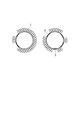
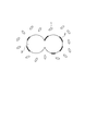
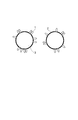
- FIG. 4 is a schematic diagram showing a state in which the metal particle surface protective material shown in FIG. 3 is detached but the metal particles cannot be sintered together. It is a schematic diagram of the metal particle which performed the surface treatment by the process which removes the surface oxide film, and the surface protection material about the metal particle with many oxide films.
- FIG. 5 It is a schematic diagram which shows the state which the surface protection material of the metal particle shown in FIG. 5 detach
- connection material of the present invention contains metal particles whose oxygen state ratio measured by X-ray photoelectron spectroscopy is less than 15%.
- the oxygen state ratio is preferably less than 10%, and more preferably less than 5%.
- the “state ratio” is the concentration of a specific element in the measurement sample, and is represented by a value calculated from the element strength using the relative sensitivity coefficient attached to the apparatus. Note that the oxygen state ratio of the metal particles measured by X-ray photoelectron spectroscopy is an index of the amount of the oxide film on the surface of the metal particles.
- metal particles various known particles can be used. Examples thereof include conductive powders such as gold, platinum, silver, copper, nickel, palladium, iron, and aluminum. These metal particles can be used alone or in combination of two or more. . Of these, silver and copper are particularly desirable in terms of price, electrical conductivity and thermal conductivity.
- the metal particles preferably have an average particle size of 0.1 ⁇ m or more and 50 ⁇ m or less. If the particle size is less than 0.1 ⁇ m, the production cost tends to increase, and if the particle size exceeds 50 ⁇ m, the gap between the particles is large and the thermal conductivity tends to decrease.
- the metal particles are preferably metal particles subjected to a treatment for removing an oxide film on the surface and a surface treatment with a surface protective material.
- connection material containing such metal particles is considered to have a high thermal conductivity even when heated at 200 ° C. or lower.
- the present inventors have established a metal particle surface treatment method that reduces or completely removes the oxide film of the metal particles and prevents reoxidation and aggregation of the metal particles.
- the method is shown below.
- metal particles are added to an acidic solution in which a surface protective material is dissolved and dispersed, and surface protection is performed while removing the oxide film while stirring.
- the surface protective material and the acid component physically adsorbed on the surface of the metal particles were washed with a solvent. Thereafter, the metal particles are dried under reduced pressure to remove excess solvent, and dry-treated surface-treated metal particles are obtained.
- the metal particles aggregate to form a powder having an average particle diameter equivalent to that of the particles before the oxide film treatment.
- the metal particles may not be obtained.
- a sulfuric acid, nitric acid, hydrochloric acid, acetic acid, phosphoric acid etc. can be used as an acid.
- the acid diluting solvent is also not limited, but a solvent that has good compatibility with the acid and that is excellent in the solubility and dispersibility of the surface protective material is desirable.
- the concentration of the acid in the acidic solution is preferably 1 part by weight or more when the entire acidic solution is 100 parts by weight in order to remove the oxide film, and 5 parts by weight or more when metal particles having a thick oxide film are included. More desirable. Further, if the acid concentration is too high, a large amount of metal dissolves in the solution, so that it is preferably 50 parts by weight or less, and more preferably 40 parts by weight or less in order to prevent the particles from aggregating.
- the surface protective material is preferably a compound having a terminal functional group that is well adsorbed on the metal surface.
- the compound which has a hydroxyl group, a carboxyl group, an amino group, a thiol group, and a disulfide group is mentioned, The compound which has a thiol group is preferable.
- the alkane skeleton preferably has 4 or more carbon atoms so as to be closely packed by the intermolecular force between the carbon chains. Further, in order for the metal particles to sinter at a low temperature of 200 ° C. or lower, it is more desirable that the desorption temperature of the surface protective material from the metal surface is 18 or less carbon atoms lower than 200 ° C.
- Examples of the compound having a thiol group and the main skeleton being a linear alkane skeleton include, for example, ethyl, n-propyl, i-propyl, n-butyl, i-butyl, t-butyl containing 1 to 18 carbon atoms.
- Mercaptans or cycloalkyl mercaptans such as pentyl, hexyl, dodecyl mercaptan, stearyl mercaptan include mercaptans such as cyclopentyl, cyclohexyl or cycloheptyl mercaptan containing 5 to 7 carbon atoms.
- the concentration of the surface protective material in the acidic solution is preferably 0.0001 parts by weight or more in order to prevent aggregation of the metal particles when the total amount of the acidic solution is 100 parts by weight. In order to prevent adsorption, the amount is preferably 0.1 parts by weight or less.
- the proportion of the metal particles in the connecting material is preferably 80 parts by weight or more for improving the thermal conductivity when the entire connecting material is 100 parts by weight, in order to achieve a thermal conductivity equal to or higher than that of high-temperature solder. Is more preferably 87 parts by weight or more. Further, in order to make the connecting material into a paste, the ratio of the metal particles is preferably 99 parts by weight or less when the whole connecting material is 100 parts by weight, and 95% for improving workability in a dispenser or a printing machine. It is more desirable that the amount is not more than parts by weight.
- the volatile component used in the present invention is not particularly limited as long as the metal particles are sintered when a predetermined heat history is applied to the mixture with the metal particles.
- volatile components include ethylene glycol butyl ether, ethylene glycol phenyl ether, diethylene glycol methyl ether, diethylene glycol ethyl ether, diethylene glycol butyl ether, diethylene glycol isobutyl ether, diethylene glycol hexyl ether, triethylene glycol methyl ether, diethylene glycol dimethyl ether, diethylene glycol diethyl ether, diethylene glycol diether.
- the above-mentioned volatile components can be used alone or as a mixture of two or more components as required.
- the content of the volatile component is preferably 20 parts by weight or less when the entire connection material is 100 parts by weight for improving thermal conductivity.
- the binder component (binder (A)) used in the present invention contains an organic polymer compound or a precursor thereof, and if necessary, a reactive diluent, a curing agent, a curing accelerator for improving curability, One or more of a flexible agent for stress relaxation, a diluent for improving workability, an adhesion improver, a wettability improver, an antifoaming agent, and a reactive diluent for reducing viscosity may be included. .
- the connecting material of the present invention may contain components other than those listed here.
- the organic polymer compound or a precursor thereof is not particularly limited, and for example, a thermosetting resin or a precursor thereof is preferable.
- a thermosetting resin or a precursor thereof examples include an epoxy resin, an acrylic resin, a maleimide resin, a cyanate resin, or a precursor thereof.
- a compound having a polymerizable ethylenic carbon-carbon double bond such as an acrylic resin or a maleimide resin or an epoxy resin is excellent in heat resistance and adhesiveness, and can be liquefied by using an appropriate solvent. It is preferable in terms of excellent workability.
- the said resin can be used individually or in combination of 2 or more types.
- the epoxy resin is preferably a compound having two or more epoxy groups in one molecule, and examples thereof include epoxy resins derived from bisphenol A, bisphenol F, bisphenol AD and the like and epichlorohydrone.
- Such a compound is not particularly limited as long as it is a compound having two or more epoxy groups in one molecule.
- bisphenol A type epoxy resin [AER-X8501 (Asahi Kasei Corporation, trade name) R-301 (Oilized Shell Epoxy Co., Ltd., trade name), YL-980 (Oilized Shell Epoxy Co., Ltd.
- an epoxy compound (reactive diluent) having only one epoxy group in one molecule may be included.
- an epoxy compound is used in a range that does not impair the characteristics of the connection material of the present invention, but is preferably used in a range of 0 to 30% by weight based on the total amount of the epoxy resin.
- the epoxy resin curing agent is not particularly limited.
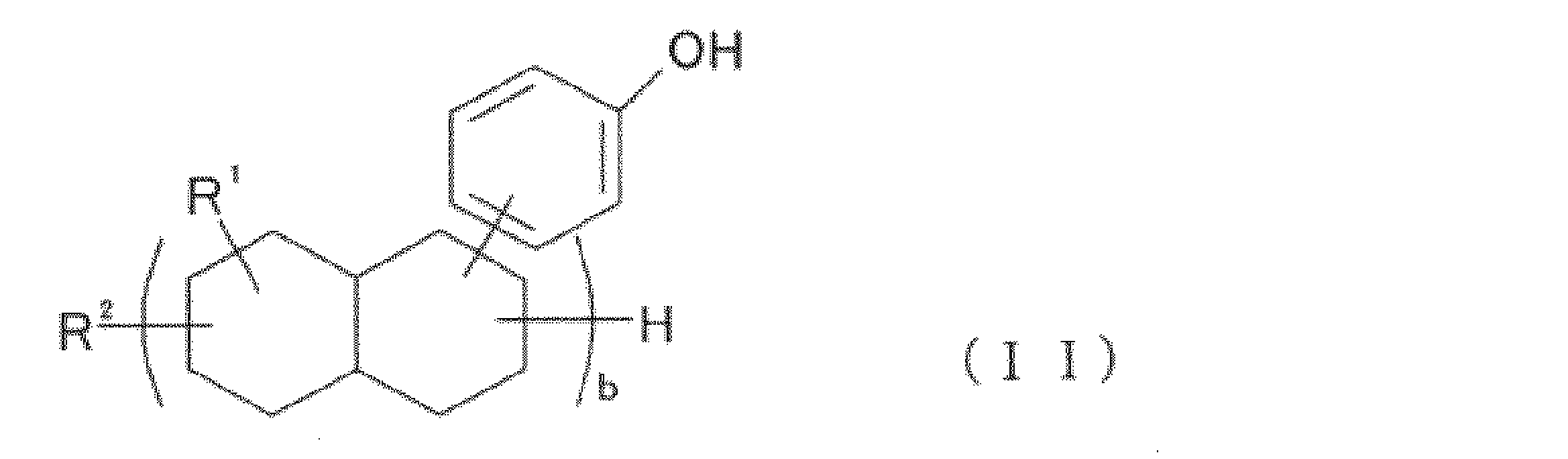
- phenol novolak resin [H-1 (Maywa Kasei Co., Ltd., trade name), VR-9300 (Mitsui Toatsu Chemicals Co., Ltd., trade name) ], Phenol aralkyl resin [XL-225 (Mitsui Toatsu Chemical Co., Ltd., trade name)], allylated phenol novolak resin [AL-VR-9300 (Mitsui Toatsu Chemical Co., Ltd., trade name)], the following general Formula (II) (Wherein R 1 represents an alkyl group having 1 to 6 carbon atoms such as a methyl group or an ethyl group, R 2 represents hydrogen or an alkyl group having 1 to 6 carbon atoms such as a methyl group or an ethyl group, and b represents 2 represents a special phenol resin [PP-700-300 (Nippon Petrochemical Co., Ltd., trade name)], bisphenol F, A, AD, allylated bisphenol F
- the compounding amount of the epoxy resin curing agent is preferably 0.01 to 90 parts by weight, more preferably 0.1 to 50 parts by weight with respect to 100 parts by weight of the epoxy resin.
- the compounding amount of the epoxy resin curing agent is less than 0.01 parts by weight, the curability tends to decrease, and when it exceeds 90 parts by weight, the viscosity increases and the workability tends to decrease.
- a curing accelerator can be added to the connection material of the present invention as necessary.
- the curing accelerator include organic boron salt compounds [EMZ ⁇ K, TPPK (Hokuko Chemical Co., Ltd., trade name)], tertiary amines or salts thereof [DBU, U-CAT102, 106, 830, 840, 5002]. (San Apro, trade name)], imidazoles [Cureazole, 2P4MHZ, C17Z, 2PZ-OK (Shikoku Kasei Co., Ltd., trade name)] and the like.
- the epoxy resin curing agent and the curing accelerator added as necessary may be used alone, or a plurality of types of epoxy resin curing agents and curing accelerators may be used in appropriate combination.
- the compounding quantity of a hardening accelerator 20 weight part or less is preferable with respect to 100 weight part of epoxy resins.
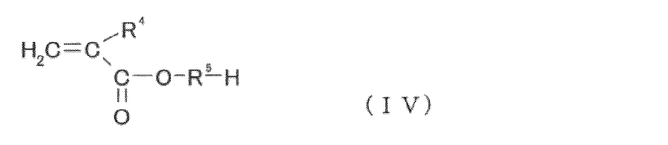
- Examples of the compound having a polymerizable ethylenic carbon-carbon double bond used in the present invention include an acrylic ester compound and a methacrylic ester compound. One or more acrylic groups or methacrylic groups are contained in one molecule.
- the compounds represented by the following general formulas (IV) to (XIII) are preferably used.
- Examples of the compound represented by the general formula (IV) include methyl acrylate, ethyl acrylate, propyl acrylate, isopropyl acrylate, n-butyl acrylate, isobutyl acrylate, t-butyl acrylate, amyl acrylate, isoamyl acrylate, hexyl acrylate, heptyl acrylate, octyl Acrylate, 2-ethylhexyl acrylate, nonyl acrylate, decyl acrylate, isodecyl acrylate, lauryl acrylate, tridecyl acrylate, hexadecyl acrylate, stearyl acrylate, isostearyl acrylate, cyclohexyl acrylate, isobornyl acrylate, tricyclo [5.2.1 .0 2,6] acrylate compounds such as decyl acrylate, methylol Methacrylate
- Examples of the compound represented by the general formula (V) include 2-hydroxyethyl acrylate, 2-hydroxypropyl acrylate, 2-hydroxyethyl methacrylate, 2-hydroxypropyl methacrylate and the like.
- Examples of the compound represented by the general formula (VI) include diethylene glycol acrylate, polyethylene glycol acrylate, polypropylene glycol acrylate, 2-methoxyethyl acrylate, 2-ethoxyethyl acrylate, 2-butoxyethyl acrylate, methoxydiethylene glycol acrylate, methoxypolyethylene glycol acrylate, Acrylate compounds such as dicyclopentenyloxyethyl acrylate, 2-phenoxyethyl acrylate, phenoxydiethylene glycol acrylate, phenoxypolyethylene glycol acrylate, 2-benzoyloxyethyl acrylate, 2-hydroxy-3-phenoxypropyl acrylate, diethylene glycol methacrylate, polyethylene glycol Methacrylate, polypropylene glycol methacrylate, 2-methoxyethyl methacrylate, 2-ethoxyethyl methacrylate, 2-butoxyethyl methacrylate, methoxydiethylene
- R 10 , R 11 and R 12 each independently represents hydrogen or an alkyl group having 1 to 6 carbon atoms
- R 13 represents hydrogen, an alkyl group having 1 to 6 carbon atoms or a phenyl group
- c represents Represents a number of 0, 1, 2, or 3].
- Examples of the compounds represented by the general formulas (VII) and (VII ′) include benzyl acrylate, 2-cyanoethyl acrylate, ⁇ -acryloyloxypropyltrimethoxysilane, glycidyl acrylate, tetrahydrofurfuryl acrylate, tetrahydropyranyl acrylate, dimethylamino Ethyl acrylate, diethylaminoethyl acrylate, 1,2,2,6,6, -pentamethylpiperidinyl acrylate, 2,2,6,6, -tetramethylpiperidinyl acrylate, acryloyloxyethyl phosphate, acryloyloxyethylphenyl Acrylate compounds such as acid phosphate, ⁇ -acryloyloxyethyl hydrogen phthalate, ⁇ -acryloyloxyethyl hydrogen succinate, Benzyl methacrylate, 2-cyanoethyl methacrylate
- Examples of the compound represented by the general formula (VIII) include ethylene glycol diacrylate, 1,4-butanediol diacrylate, 1,6-hexanediol diacrylate, 1,9-nonanediol diacrylate, and 1,3-butanediol.
- Diacrylate compounds such as diacrylate, neopentyl glycol diacrylate, dimer diol diacrylate, ethylene glycol dimethacrylate, 1,4-butanediol dimethacrylate, 1,6-hexanediol dimethacrylate, 1,9-nonanediol dimethacrylate 1, 3-butanediol dimethacrylate, neopentyl glycol dimethacrylate, dimer diol dimethacrylate and the like.
- the compound represented by the general formula (IX) includes diacrylate compounds such as diethylene glycol diacrylate, triethylene glycol diacrylate, tetraethylene glycol diacrylate, polyethylene glycol diacrylate, tripropylene glycol diacrylate, polypropylene glycol diacrylate, and diethylene glycol.
- diacrylate compounds such as diethylene glycol diacrylate, triethylene glycol diacrylate, tetraethylene glycol diacrylate, polyethylene glycol dimethacrylate, tripropylene glycol dimethacrylate, and polypropylene glycol dimethacrylate.
- Examples of the compound represented by the general formula (X) include a reaction product of 1 mol of bisphenol A, bisphenol F or bisphenol AD and 2 mol of glycidyl acrylate, a reaction product of 1 mol of bisphenol A, bisphenol F or bisphenol AD and 2 mol of glycidyl methacrylate, and the like. There is.
- the compound represented by the general formula (XI) includes diacrylate of bisphenol A, bisphenol F or polyethylene oxide adduct of bisphenol AD, diacrylate of bisphenol A, bisphenol F or polypropylene oxide adduct of bisphenol AD, bisphenol A, bisphenol.
- Examples include dimethacrylate of polyethylene oxide adduct of F or bisphenol AD, dimethacrylate of polypropylene oxide adduct of bisphenol A, bisphenol F or bisphenol AD.
- Examples of the compound represented by the general formula (XII) include bis (acryloyloxypropyl) polydimethylsiloxane, bis (acryloyloxypropyl) methylsiloxane-dimethylsiloxane copolymer, bis (methacryloyloxypropyl) polydimethylsiloxane, and bis (methacryloyloxypropyl). ) Methylsiloxane-dimethylsiloxane copolymer.
- Examples of the compound represented by the general formula (XIII) include a reaction product obtained by reacting a polybutadiene to which maleic anhydride is added and an acrylic ester compound or a methacrylic ester compound having a hydroxyl group in the molecule, and a hydrogenated product thereof. Yes, as long as it is a compound having one or more acrylic or methacrylic groups in one molecule, for example, MM-1000-80, MAC-1000-80 (both products of Nippon Petrochemical Co., Ltd.) Name).
- the above compounds can be used alone or in combination of two or more.
- thermosetting resin When a compound having an ethylenic carbon-carbon double bond is used as the thermosetting resin, it is preferable to use a radical initiator in combination as a curing agent catalyst.
- the radical initiator is not particularly limited, but a peroxide is preferable from the viewpoint of voids and the like, and a peroxide decomposition temperature of 70 to 170 ° C. is preferable from the viewpoint of curability and viscosity stability of the connecting material. .
- radical initiator examples include 1,1,3,3-tetramethylperoxy 2-ethylhexanoate, 1,1-bis (t-butylperoxy) cyclohexane, 1,1-bis (t- Butylperoxy) cyclododecane, di-t-butylperoxyisophthalate, t-butylperbenzoate, dicumyl peroxide, t-butylcumyl peroxide, 2,5-dimethyl-2,5-di (t-butyl) Peroxy) hexane, 2,5-dimethyl-2,5-di (t-butylperoxy) hexyne, cumene hydroperoxide and the like.
- the blending amount of the radical initiator is preferably 0.1 to 10 parts by weight, particularly preferably 0.5 to 5 parts by weight based on 100 parts by weight of the total amount of compounds having a polymerizable ethylenic carbon-carbon double bond. .
- the above-mentioned binder component can be used alone or as a mixture of two or more components as required.
- the content of the binder component is preferably 3 to 30 parts by weight when the entire connecting material is 100 parts by weight.
- the flexing agent examples include liquid polybutadiene (acrylonitrile butadiene copolymers such as “CTBN-1300 ⁇ 31” and “CTBN-1300 ⁇ 9” manufactured by Ube Industries, Ltd.), and epoxy, carboxyl, Those having at least one functional group selected from an amino group and a vinyl group are preferred.
- liquid polybutadiene acrylonitrile butadiene copolymers such as “CTBN-1300 ⁇ 31” and “CTBN-1300 ⁇ 9” manufactured by Ube Industries, Ltd.
- epoxy carboxyl
- an organic solvent having a relatively high boiling point such as butyl cellosolve, carbitol, butyl cellosolve, carbitol acetate, ethylene glycol diethyl ether, ⁇ -terpineol can be used.
- the number average molecular weight of the acrylonitrile butadiene copolymer is preferably 500 to 10,000. When the molecular weight is less than 500, the chip warp reducing effect tends to be inferior, and when the molecular weight exceeds 10,000, the viscosity of the connecting material tends to increase and the workability tends to be inferior.
- the number average molecular weight is a value measured by a vapor pressure osmosis method or a value measured by a gelation chromatography using a standard polystyrene calibration curve (hereinafter referred to as GPC method).
- the epoxidized polybutadiene preferably has an epoxy equivalent of 100 to 500 (g / eq).
- the epoxy equivalent is less than 100, the viscosity increases, and the workability of the connecting material tends to decrease.
- the epoxy equivalent exceeds 500, the adhesive strength during heating tends to decrease.
- the epoxy equivalent is determined by the perchloric acid method. Epoxy polybutadiene having a hydroxyl group in the molecule may be used.
- the number average molecular weight of the epoxidized polybutadiene is preferably 500 to 10,000. When the molecular weight is less than 500, the chip warp reducing effect tends to be inferior, and when the molecular weight exceeds 10,000, the viscosity of the connecting material tends to increase and the workability tends to be inferior.
- the number average molecular weight is a value measured by the GPC method.
- the flexible agent has an effect of relieving stress generated by bonding the semiconductor element and the lead frame.
- the flexible agent is usually added in an amount of 0 to 500 parts by weight when the total amount of the organic polymer compound and its precursor is 100 parts by weight.
- connection material of the present invention further improves the adhesive strength of a hygroscopic agent such as calcium oxide and magnesium oxide, a silane coupling agent, a titanate coupling agent, an aluminum coupling agent, and a zircoaluminate coupling agent.
- a hygroscopic agent such as calcium oxide and magnesium oxide, a silane coupling agent, a titanate coupling agent, an aluminum coupling agent, and a zircoaluminate coupling agent.
- Agents, nonionic surfactants, wetting improvers such as fluorosurfactants, antifoaming agents such as silicone oil, ion trapping agents such as inorganic ion exchangers, polymerization inhibitors, and the like can be added as appropriate.
- silane coupling agent for example, vinyl tris ( ⁇ -methoxyethoxy) silane, vinyltriethoxysilane, vinyltrimethoxysilane, ⁇ -methacryloxypropyltrimethoxysilane, ⁇ - (3,4-epoxycyclohexyl) Ethyltrimethoxysilane, ⁇ -glycidoxypropyltrimethoxysilane, ⁇ -glycidoxypropylmethyldiethoxysilane, N-phenyl- ⁇ -aminopropyltrimethoxysilane, ⁇ -mercaptopropyltrimethoxysilane, hexamethyldisilazane N, O- (bistrimethylsilyl) acetamide, N-methyl-3-aminopropyltrimethoxysilane, 4,5-dihydroimidazolepropyltriethoxysilane, ⁇ -mercaptopropyltriethoxysilane,
- titanate coupling agent examples include isopropyl triisostearoyl titanate, isopropyl trioctanoyl titanate, isopropyl dimethacrylisostearoyl titanate, isopropyl tridodecylbenzenesulfonyl titanate, isopropyl isostearoyl diacryl titanate, isopropyl tri (dioctyl phosphate) titanate.
- polymerization inhibitor examples include quinones, hydroquinone, nitro / nitroso compounds, amines, polyoxy compounds, p-tert-butylcatechol, picric acid, dithiobenzoyl disulfide and other sulfur-containing compounds, cupric chloride, diphenylpicrin.
- examples include, but are not limited to, hydrazyl, tri-p-nitrophenylmethyl, triphenylferdazyl, N- (3-N-oxyanilino-1,3-dimethylbutylidene) aniline oxide, and the like.
- the bleed inhibitor can be further added to the connection material of the present invention as necessary.
- bleed inhibitors include fatty acids such as perfluorooctanoic acid, octanoic acid amide, and oleic acid, perfluorooctylethyl acrylate, silicone, and the like.
- filler (B) various known materials, for example, conductive powders such as gold, platinum, silver, copper, nickel, palladium, iron, and aluminum can be used. Moreover, these fillers can be used individually or in combination of 2 or more types. Of these, silver and copper are particularly desirable in terms of price, electrical conductivity and thermal conductivity.
- the additive (C) As the additive (C), the above-mentioned volatile components and surface protective agents can be used.
- the metal particles, the volatile component and the binder are mixed or divided together with a diluent added as necessary, and the stirrer, the raider, the three rolls, the planetary mixer.
- the dispersing / dissolving devices such as the above may be appropriately combined, and heated, if necessary, mixed, dissolved, granulated and kneaded or dispersed to form a uniform paste.
- FIG. 7 is a schematic cross-sectional view showing an example of a semiconductor device manufactured using the connection material of the present invention.
- the semiconductor device shown in FIG. 7 includes three lead frames (heat radiating bodies) 12a, 12b, and 12c, a chip (heating element) 11 connected to the lead frame 12a via the connecting material of the present invention, and these. It consists of a mold resin 15 to be molded.
- the chip 11 is connected to lead frames 12b and 12c via two wires 14, respectively.
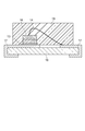
- FIG. 8 is a schematic cross-sectional view showing another example of a semiconductor device manufactured using the connection material of the present invention.
- the semiconductor device shown in FIG. 7 includes a substrate 16, two lead frames 17 formed so as to surround the substrate, an LED chip 18 connected to the lead frame 17 via the connection material of the present invention, and these It consists of translucent resin 19 which seals.
- the LED chip 18 is connected to the lead frame 17 via the wire 14.
- the semiconductor device of the present invention can be obtained by bonding a semiconductor element to a support member using the connection material of the present invention. After bonding the semiconductor element to the support member, a wire bonding step and a sealing step are performed as necessary.
- supporting members include lead frames such as 42 alloy lead frames, copper lead frames, palladium PPF lead frames, glass epoxy substrates (substrates made of glass fiber reinforced epoxy resins), BT substrates (cyanate monomers and oligomers thereof, and bismaleimides). Organic substrates such as a BT resin substrate).
- connection material is applied on the support member by a dispensing method, a screen printing method, a stamping method, etc., and then the semiconductor element is crimped. Then, it can be carried out by heating and curing using a heating device such as an oven or a heat block. Heat curing is usually performed by heating at 100 to 200 ° C. for 5 seconds to 10 hours. Furthermore, it can be set as the completed semiconductor device by sealing by a normal method after passing through a wire bond process.
- Curing accelerator 2 PZCNS-PW (Shikoku Kasei Kogyo Co., Ltd., trade name, imidazole) 1.1 parts by weight
- Volatile components Dipropylene glycol methyl ether acetate (hereinafter referred to as DMPA) (Daicel Chemical Co., Ltd.), Toluene (Kanto Chemical Co., Ltd.), ⁇ -butyrolactone (Sankyo Chemical Co., Ltd.)
- An acidic solution was prepared by diluting 28 parts by weight of hydrochloric acid (Kanto Chemical Co., Ltd.) with 80 parts by weight of ethanol (Kanto Chemical Co., Ltd.). To this acidic solution, 0.29 parts by weight of stearyl mercaptan (Tokyo Chemical Industry Co., Ltd.) was added as a surface protective material to prepare a surface treatment solution.
- AgF10S was added to the surface treatment solution, and the oxide film was removed and the surface treatment was performed by stirring for 1 hour while maintaining the temperature at 40 ° C. Thereafter, the surface treatment solution was removed by filtration, and ethanol at 40 ° C. was added to wash the surface-treated Ag powder.
- the ethanol washing solution was removed by filtration, and the washing and filtration steps were repeated about 10 times to remove stearyl mercaptan and hydrochloric acid physically adsorbed on the surface-treated Ag powder surface.
- the surface-treated Ag powder after washing was dried under reduced pressure to remove ethanol to obtain a dried surface-treated Ag powder.
- the obtained surface-treated Ag powder had an oxygen state ratio of 0%, and it was confirmed that the oxide film was completely removed.
- the materials (1) and (2) were kneaded for 10 minutes with a rough machine to obtain a binder component.
- materials (3) and (4) were added at the blending ratio shown in Table 1, and kneaded for 15 minutes with a rough machine to obtain a connection material.
- the characteristics of the connecting material were examined by the following method. Tables 1 and 2 show the composition of the metal particles, the volatile component and the binder component, and the measurement results of the characteristics.
- connection material was heat treated at 180 ° C. for 1 hour to obtain a 10 ⁇ 10 ⁇ 1 mm test piece.
- the thermal diffusivity of this test piece was measured by a laser flash method (manufactured by Netch, LFA 447, 25 ° C.), and this thermal diffusivity and the ratio obtained with a differential scanning calorimeter (Pyris 1 manufactured by Perkin Elmer) From the product of the heat capacity and the specific gravity obtained by the Archimedes method, the cured product thermal conductivity (W / m ⁇ K) of the connection material at 25 ° C. was calculated.
- connection material composed of the surface-treated Ag powders of Examples 1 to 3 and the volatile components has a high thermal conductivity of 70 W / m ⁇ K or higher, and a high of 7 MPa or higher at 260 ° C. It is clear that the share strength is developed.
- the connecting material consisting of Ag powder (AgF10S) with an oxygen state ratio of 15% or more and a volatile component does not cause sintering between metal particles at 180 ° C. It is clear that a test specimen for measurement cannot be produced and no shear strength is developed.
- the connecting material composed of Ag powder (AgF10S) having an oxygen state ratio of 15% or more, a volatile component, and a binder component has a low thermal conductivity of 3 W / m ⁇ K or less. It is apparent that the connecting material composed of the surface-treated Ag powder, the volatile component, and the binder component exhibits a high thermal conductivity of 20 W / m ⁇ K or more while maintaining the shear strength.
- connection material consisting of AgF10S having an oxygen state ratio of 15% or more and a binder component from Reference Example 5 has a low thermal conductivity of 2 W / m ⁇ K or less, but from the surface-treated AgF10S of Example 5 and the binder component. It is apparent that the resulting connecting material exhibits a high thermal conductivity of 20 W / m ⁇ K or more while maintaining the shear strength.
- connection material composed of the surface-treated AgF5S with the oxygen state ratio of 10% and the volatile component and the binder component from Examples 6 and 7 is AgF5S with the oxygen state ratio of 20% or more shown in Reference Examples 6 and 7. It is clear that higher thermal conductivity and shear strength are exhibited than the connection material composed of the volatile component and the binder component.
- Binder (A) is 37.6 parts by weight of epoxy resin solution (A1), 9.2 parts by weight of acrylotonyl butadiene copolymer (A2), 18.4 parts by weight of epoxidized polybutadiene (A3), and epoxy resin curing agent.
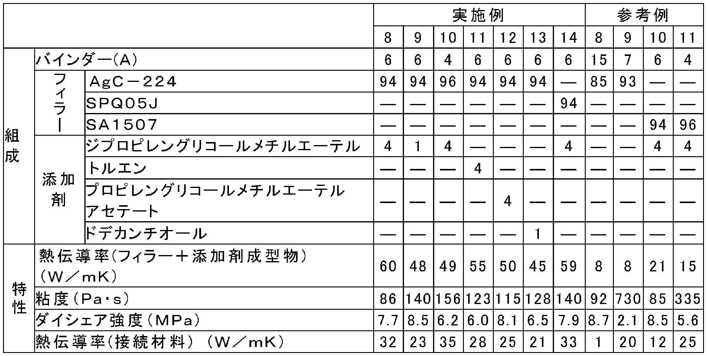
- the prepared binder (A), filler (B) and additive (C) were mixed at the blending ratio shown in Table 3, kneaded for 15 minutes with a rough machine, then kneaded at 5 Torr or less, The connection materials of Examples 8 to 14 and Reference Examples 8 to 11 were obtained.
- connection materials of Examples 8 to 14 and Reference Examples 8 to 11 and the characteristics of the molded mixture of filler (B) and additive (C) were measured by the following methods. The results are shown in Table 3.
- Viscosity Using an EHD type rotational viscometer (manufactured by Tokyo Keiki Co., Ltd.), the viscosity (Pa ⁇ s) at 25 rpm at 25 ° C. of the connecting material was measured.
- Die shear strength (shear strength): About 0.2 mg of a connecting material is applied on a palladium-plated lead frame (PPF, land portion: 10 ⁇ 8 mm), and a 2 mm ⁇ 2 mm silicon chip (thickness) 0.4 mm) and further heat-treated at 180 ° C. for 1 hour in a clean oven (Espec Corp.).
- the thermal diffusivity of this molded product was measured by a laser flash method (manufactured by Netch, LFA 447, 25 ° C.), and this thermal diffusivity and a ratio obtained by a differential scanning calorimeter (Pyris 1 manufactured by Perkin Elmer) From the product of the heat capacity and the specific gravity obtained by the Archimedes method, the thermal conductivity (W / m ⁇ K) of the cured product of the mixture of the filler (B) and the additive (C) at 25 ° C. was calculated.
- (4) Thermal conductivity of cured product of connection material The connection material was heat-treated at 180 ° C. for 1 hour to obtain a 10 ⁇ 10 ⁇ 1 mm test piece.
- the thermal diffusivity of this test piece was measured by a laser flash method (manufactured by Netch, LFA 447, 25 ° C.), and the thermal diffusivity and the ratio obtained with a differential scanning calorimeter (Pyris 1 manufactured by PerkinElmer) From the product of the heat capacity and the specific gravity obtained by the Archimedes method, the cured product thermal conductivity (W / m ⁇ K) of the connection material at 25 ° C. was calculated.
- connection materials of Examples 8 to 14 the viscosity is excellent in workability, and it is possible to improve the thermal conductivity while maintaining the adhesive strength.
- the thermal conductivity of the mixture molded body of the filler (B) and the additive (C) is low, and the thermal conductivity of the cured body of the connection material is also low.
- the connection material of Reference Example 9 containing no additive has a relatively high thermal conductivity of the cured product of the connection material, but has a high content ratio of the filler (B), so the viscosity of the connection material is high.
- connection material of Reference Example 10 contains an additive, since the thermal conductivity of the mixture molded body of the filler (B) and the additive (C) is low, the thermal conductivity of the cured body of the connection material is low. Lower.
- the connection material of Reference Example 11 has an additive, and the cured product of the connection material has high thermal conductivity, but the mixture molded body of the filler (B) and additive (C) has low thermal conductivity. The viscosity of the connecting material is high.
Landscapes
- Chemical & Material Sciences (AREA)
- Organic Chemistry (AREA)
- Engineering & Computer Science (AREA)
- Inorganic Chemistry (AREA)
- Manufacturing & Machinery (AREA)
- Microelectronics & Electronic Packaging (AREA)
- Adhesives Or Adhesive Processes (AREA)
- Conductive Materials (AREA)
- Die Bonding (AREA)
- Powder Metallurgy (AREA)
- Connections Effected By Soldering, Adhesion, Or Permanent Deformation (AREA)
- Non-Insulated Conductors (AREA)
- Pigments, Carbon Blacks, Or Wood Stains (AREA)
- Other Surface Treatments For Metallic Materials (AREA)
Abstract
Description
次に、溶液をろ過して金属粒子を取り出した後、金属粒子表面に物理的に吸着した表面保護材や酸成分を溶媒で洗浄した。その後、金属粒子を減圧乾燥させることで余分な溶媒を除去し、乾燥状態の表面処理された金属粒子を得る。
また、酸の濃度が濃すぎると金属が多量に溶液に溶けてしまうため、50重量部以下が望ましく、粒子同士が凝集を防ぐためには40重量部以下がより望ましい。
また金属粒子の再酸化や余分な有機物の吸着汚染をさらに高度に防止するために、化合物の主骨格は保護材が密に充填されるような直鎖アルカン骨格を持つものが望ましい。
また、200℃以下の低い温度で金属粒子が焼結するために、表面保護材の金属表面からの脱離温度が200℃より低い炭素数18個以下がより望ましい。
チオール基を有し、主骨格が直鎖アルカン骨格である化合物としては、例えば、1乃至18炭素原子を含む、エチル、n-プロピル、i-プロピル、n-ブチル、i-ブチル、t-ブチル、ペンチル、ヘキシル、ドデシルメルカプタン、ステアリルメルカプタンのようなメルカプタン又はシクロアルキルメルカプタンは、5乃至7炭素原子を含む、シクロペンチル、シクロヘキシル又はシクロヘプチルメルカプタンのようなメルカプタンなどが挙げられる。
また、接続材料をペースト状にするためには金属粒子の割合は、接続材料全体を100重量部としたとき、99重量部以下が望ましく、ディスペンサーや印刷機での作業性向上のために、95重量部以下であることがより望ましい。
揮発性成分の一例として、エチレングリコールブチルエーテル、エチレングリコールフェニルエーテル、ジエチレングリコールメチルエーテル、ジエチレングリコールエチルエーテル、ジエチレングリコールブチルエーテル、ジエチレングリコールイソブチルエーテル、ジエチレングリコールヘキシルエーテル、トリエチレングリコールメチルエーテル、ジエチレングリコールジメチルエーテル、ジエチレングリコールジエチルエーテル、ジエチレングリコールジブチルエーテル、ジエチレングリコールブチルメチルエーテル、ジエチレングリコールイソプロピルメチルエーテル、トリエチレングリコールジメチルエーテル、トリエチレングリコールブチルメチルエーテル、エチレングリコールエチルエーテルアセテート、エチレングリコールブチルエーテルアセテート、ジエチレングリコールエチルエーテルアセテート、ジエチレングリコールブチルエーテルアセテート、プロピレングリコールプロピルエーテル、ジプロピレングリコールメチルエーテル、ジプロピレングリコールエチルエーテル、ジプロピレングリコールプロピルエーテル、ジプロピレングリコールブチルエーテル、ジプロピレングリコールジメチルエーテル、トリプロピレングリコールメチルエーテル、トリプロピレングリコールジメチルエーテル、ジプロピレングリコールメチルエーテルアセテート、3-メチル-3-メトキシブタノール、乳酸エチル、乳酸ブチル、γ-ブチロラクトン、α-テルピネオール、イソホロン、p-シメン、1,3-ジメチル-2-イミダゾリジノン、アニソール、ジメチルスルホキシド、ヘキサメチルホスホリルアミド、m-クレゾール、o-クロルフェノール、セロソルブアセテート、N-メチル-2-ピロリドン、N,N-ジメチルアセトアミド、N,N-ジメチルホルムアミド、スルホラン、テトラヒドロフラン、ジオキサン、モノグライム、ジグライム、ベンゼン、トルエン、キシレン、メチルエチルケトン、メチルセロソルブ、セロソルブアセテート、シクロヘキサノン等が挙げられる。





(3)揮発性成分: ジプロピレングリコールメチルエーテルアセテート(以下、DMPAという)(ダイセル化学(株))、トルエン(関東化学(株))、γ-ブチロラクトン(三協化学(株))
また、以下の手順でAgF10Sの酸化膜除去及び表面処理を施した表面処理Ag粉を作製した。
次に、表1に示す配合割合で、材料(3)及び(4)を加えてらいかい機で15分間混練し、接続材料を得た。
接続材料の特性を下記に示す方法で調べた。金属粒子、揮発性成分及びバインダー成分の組成、並びに特性の測定結果を表1及び表2に示す。


下記のバインダー(A)、フィラー(B)及び添加剤(C)を準備した。
バインダー(A):
バインダー(A)は、エポキシ樹脂溶液(A1)37.6重量部、アクリロニトニルブタジエン共重合体(A2)9.2重量部、エポキシ化ポリブタジエン(A3)18.4重量部、エポキシ樹脂硬化剤(A4)1.8重量部、硬化促進剤(A5)0.8重量部、希釈剤(A6)18.2重量部、メタクリル酸エステル化合物(A7)14.7重量部及びラジカル開始剤(A8)0.5重量部を、らいかい機にて10分間混練することにより調製した。
エポキシ樹脂溶液(A1):YDF-170(東都化成株式会社、商品名、ビスフェノールF型エポキシ樹脂、エポキシ当量=170)7.5重量部及びYL-980(ジャパンエポキシレジン株式会社、商品名、ビスフェノールA型エポキシ樹脂、エポキシ当量=185)7.5重量部を80℃に加熱し、1時間撹拌を続け、均一なエポキシ樹脂溶液を得た。
アクリロニトニルブタジエン共重合体(A2):
CTBNX-1300×9(宇部興産株式会社、商品名、カルボキシル基末端アクリロニトニルブタジエン共重合体)
エポキシ化ポリブタジエン(A3):
E-1000-8.0(日本石油化学株式会社、商品名)
エポキシ樹脂硬化剤(A4):
ジシアンジアミド
硬化促進剤(A5):
C17Z(四国化成株式会社、商品名、イミダゾール)
希釈剤(A6):
PP-101(東都化成株式会社、商品名、アルキルフェニルグリシジルエーテル)
メタクリル酸エステル化合物(A7):
エチレングリコールジメタクリレート
ラジカル開始剤(A8):
ジクミルパーオキサイド
フィラー(B):
AgC-224(福田金属箔粉株式会社、商品名、銀粉、平均粒子径10μm)
SPQ05J(三井金属鉱業株式会社、商品名、銀粉、平均粒子径0.85μm)
SA1507(メタロー、商品名、銀粉、平均粒子径15μm)
添加剤(C):
ジプロピレングリコールメチルエーテル
トルエン
プロピレングリコールメチルエーテルアセテート
ドデカンチオール
(2)ダイシェア強度(剪断強さ):接続材料をパラジウムめっきリードフレーム(PPF、ランド部:10×8mm)上に約0.2mgを塗布し、この上に2mm×2mmのシリコンチップ(厚さ 0.4mm)を圧着し、さらにクリーンオーブン(エスペック社製)で180℃、1時間加熱処理した。これを万能型ボンドテスタ(デイジ社製、4000シリーズ)を用いて、測定スピード500μm/s、測定高さ120μmで260℃で30秒加熱した後の剪断強さ(MPa)を測定した。
(3)フィラー(B)と添加剤(C)との混合物成型体の熱伝導率:フィラー(B)と添加剤(C)とを表3に示す配合割合で、総重量が20gとなるように配合し、乳鉢等で混練した。生成した粉体状あるいはペースト状の混合物を10×10×1mmとなるように成型し180℃、1時間加熱処理した。この成型物の熱拡散率をレーザーフラッシュ法(ネッチ社製、LFA 447、25℃)で測定し、さらにこの熱拡散率と、示差走査熱量測定装置(パーキンエルマー社製 Pyris1)で得られた比熱容量とアルキメデス法で得られた比重の積より、25℃におけるフィラー(B)と添加剤(C)との混合物成型体の硬化物の熱伝導率(W/m・K)を算出した。
(4)接続材料の硬化物の熱伝導率:上記接続材料を180℃、1時間加熱処理し、10×10×1mmの試験片を得た。この試験片の熱拡散率をレーザーフラッシュ法(ネッチ社製、LFA 447、25℃)で測定し、さらにこの熱拡散率と、示差走査熱量測定装置(パーキンエルマー社製 Pyris1)で得られた比熱容量とアルキメデス法で得られた比重の積より、25℃における接続材料の硬化物熱伝導率(W/m・K)を算出した。
Claims (8)
- X線光電子分光法で測定される酸素の状態比率が15%未満である金属粒子を含有する接続材料。
- 前記金属粒子は、その表面の酸化膜を除去する処理及び表面保護材による表面処理を施した金属粒子である、請求項1記載の接続材料。
- 前記金属粒子の平均粒子径は0.1μm以上50μm以下である、請求項1又は2記載の接続材料。
- 前記金属粒子は200℃以下で焼結された金属粒子である、請求項1~3のいずれかに記載の接続材料。
- 揮発性成分又はバインダー成分をさらに含有してなる、請求項1~4のいずれかに記載の接続材料。
- バインダー(A)、フィラー(B)及び添加剤(C)を含む接続材料であって、
前記フィラー(B)と前記添加剤(C)とを、前記接続材料における重量比と同じ重量比で混合し、加熱成型した成型体の熱伝導率が40W/mK以上となる接続材料。 - 前記添加剤(C)の含有量が、バインダー(A)100重量部に対して1~100重量部である、請求項6に記載の接続材料。
- 請求項1~7のいずれかに記載の接続材料を介して、半導体素子と半導体素子搭載用支持部材が接着された構造を有する半導体装置。
Priority Applications (5)
| Application Number | Priority Date | Filing Date | Title |
|---|---|---|---|
| US12/990,082 US8421247B2 (en) | 2008-04-30 | 2009-04-28 | Connecting material having metallic particles of an oxygen state ratio and size and semiconductor device having the connecting material |
| JP2010510144A JP5921808B2 (ja) | 2008-04-30 | 2009-04-28 | 接続材料及び半導体装置 |
| CN2009801151612A CN102017016A (zh) | 2008-04-30 | 2009-04-28 | 连接材料和半导体装置 |
| KR1020107026727A KR101311681B1 (ko) | 2008-04-30 | 2009-04-28 | 접속 재료 및 반도체 장치 |
| EP09738834.2A EP2278593A4 (en) | 2008-04-30 | 2009-04-28 | CONNECTING MATERIAL AND SEMICONDUCTOR ARRANGEMENT |
Applications Claiming Priority (2)
| Application Number | Priority Date | Filing Date | Title |
|---|---|---|---|
| JP2008118418 | 2008-04-30 | ||
| JP2008-118418 | 2008-04-30 |
Publications (1)
| Publication Number | Publication Date |
|---|---|
| WO2009133897A1 true WO2009133897A1 (ja) | 2009-11-05 |
Family
ID=41255113
Family Applications (1)
| Application Number | Title | Priority Date | Filing Date |
|---|---|---|---|
| PCT/JP2009/058375 Ceased WO2009133897A1 (ja) | 2008-04-30 | 2009-04-28 | 接続材料及び半導体装置 |
Country Status (8)
| Country | Link |
|---|---|
| US (1) | US8421247B2 (ja) |
| EP (1) | EP2278593A4 (ja) |
| JP (3) | JP5921808B2 (ja) |
| KR (1) | KR101311681B1 (ja) |
| CN (3) | CN104962214A (ja) |
| MY (1) | MY152082A (ja) |
| TW (1) | TWI532818B (ja) |
| WO (1) | WO2009133897A1 (ja) |
Cited By (10)
| Publication number | Priority date | Publication date | Assignee | Title |
|---|---|---|---|---|
| WO2012043545A1 (ja) * | 2010-09-29 | 2012-04-05 | 日立化成工業株式会社 | 接着剤組成物及びそれを用いた半導体装置 |
| WO2012102275A1 (ja) * | 2011-01-28 | 2012-08-02 | 日立化成工業株式会社 | 接着剤組成物及びそれを用いた半導体装置 |
| CN102841503A (zh) * | 2012-09-18 | 2012-12-26 | 江苏科技大学 | 一种用于触摸屏的光刻电子银胶组合物及其制备方法 |
| JP2015025028A (ja) * | 2013-07-24 | 2015-02-05 | 日立化成株式会社 | 接続材料、これを用いた接続構造体及びその製造方法 |
| EP2428293A3 (de) * | 2010-09-03 | 2016-08-10 | Heraeus Deutschland GmbH & Co. KG | Kontaktierungsmittel und Verfahren zur Kontaktierung elektrischer Bauteile |
| WO2017006854A1 (ja) * | 2015-07-08 | 2017-01-12 | 住友ベークライト株式会社 | 熱伝導性組成物、半導体装置、半導体装置の製造方法、および放熱板の接着方法 |
| JP2020041045A (ja) * | 2018-09-10 | 2020-03-19 | デクセリアルズ株式会社 | 接着剤組成物 |
| JP2021182610A (ja) * | 2020-05-20 | 2021-11-25 | 日亜化学工業株式会社 | 発光装置の検査方法及び検査用治具 |
| WO2022239806A1 (ja) * | 2021-05-14 | 2022-11-17 | 住友ベークライト株式会社 | 銀含有ペースト |
| JP2023153928A (ja) * | 2015-05-08 | 2023-10-18 | ヘンケル・アクチェンゲゼルシャフト・ウント・コムパニー・コマンディットゲゼルシャフト・アウフ・アクチェン | 焼結可能フィルムおよびペーストおよびその使用方法 |
Families Citing this family (17)
| Publication number | Priority date | Publication date | Assignee | Title |
|---|---|---|---|---|
| JPH076119B2 (ja) | 1987-08-31 | 1995-01-25 | トヨタ自動車株式会社 | 起毛ニット |
| JP5218364B2 (ja) * | 2009-10-02 | 2013-06-26 | 横浜ゴム株式会社 | 熱伝導性組成物 |
| TWI598411B (zh) * | 2012-05-29 | 2017-09-11 | 巴斯夫歐洲公司 | 用於印刷墨水及塗層之水基聚合物組成物 |
| CN104350814B (zh) * | 2012-06-15 | 2017-10-13 | 株式会社钟化 | 散热结构体、便携式信息终端、电子设备及电子设备的修理方法 |
| DE102012222416A1 (de) | 2012-12-06 | 2014-06-12 | Robert Bosch Gmbh | Verfahren zum Verbinden von wenigstens zwei Komponenten unter Verwendung eines Sinterprozesses |
| FR3041210B1 (fr) * | 2015-09-15 | 2017-09-15 | Sagem Defense Securite | Procede d'assemblage par frittage d'argent sans pression |
| JP7081064B2 (ja) * | 2016-01-19 | 2022-06-07 | ナミックス株式会社 | 樹脂組成物、導電性銅ペースト、および半導体装置 |
| TWI637470B (zh) * | 2016-04-19 | 2018-10-01 | Kabushiki Kaisha Toshiba | 半導體封裝及其之製造方法 |
| US20190264070A1 (en) * | 2016-10-31 | 2019-08-29 | Sumitomo Bakelite Co., Ltd. | Thermally conductive paste and electronic device |
| JP6776973B2 (ja) * | 2017-03-28 | 2020-10-28 | 日油株式会社 | 表面被覆銅フィラー中間体の製造方法 |
| JP6998713B2 (ja) * | 2017-09-25 | 2022-02-04 | 古河電気工業株式会社 | 金属微粒子含有組成物 |
| CN111033640A (zh) * | 2017-09-27 | 2020-04-17 | 京瓷株式会社 | 膏组合物、半导体装置以及电气电子部件 |
| WO2020227531A1 (en) | 2019-05-07 | 2020-11-12 | Bridgestone Americas Tire Operations, Llc | Modified high-cis polybutadiene polymer, related methods and rubber compositions |
| US12264232B2 (en) | 2019-05-14 | 2025-04-01 | Bridgestone Corporation | Modified high-cis polybutadiene polymer, related methods and tire components |
| CN112238223A (zh) * | 2019-07-18 | 2021-01-19 | 上栗县科源冶金材料有限公司 | 一种用于金属粉末存放的防氧化方法 |
| CN112080238B (zh) * | 2020-09-07 | 2022-05-27 | 江苏矽时代材料科技有限公司 | 一种导热填充胶及其制备方法和应用 |
| CN117461120A (zh) * | 2021-06-07 | 2024-01-26 | 住友电木株式会社 | 导电性膏、固化物和半导体装置 |
Citations (6)
| Publication number | Priority date | Publication date | Assignee | Title |
|---|---|---|---|---|
| JPH1166953A (ja) | 1997-08-22 | 1999-03-09 | Sumitomo Metal Mining Co Ltd | 導電性接着剤およびその使用方法 |
| JP2003206469A (ja) * | 2001-11-12 | 2003-07-22 | Hitachi Chem Co Ltd | 接着剤組成物及びこれを用いた半導体装置 |
| JP2005093996A (ja) | 2003-09-15 | 2005-04-07 | Fujitsu Ltd | 熱的な界面の接着剤 |
| JP2006073811A (ja) | 2004-09-02 | 2006-03-16 | Kyocera Chemical Corp | ダイボンディングペースト |
| JP2006083377A (ja) | 2004-08-18 | 2006-03-30 | Harima Chem Inc | 導電性接着剤および該導電性接着剤を利用する物品の製造方法 |
| JP2006302834A (ja) | 2005-04-25 | 2006-11-02 | Kyocera Chemical Corp | ダイボンディングペースト |
Family Cites Families (23)
| Publication number | Priority date | Publication date | Assignee | Title |
|---|---|---|---|---|
| NL283747A (ja) * | 1961-09-28 | |||
| JPH08259842A (ja) * | 1995-03-17 | 1996-10-08 | Daiken Kagaku Kogyo Kk | 被覆無機粉体およびその製造法 |
| US5939824A (en) * | 1995-05-30 | 1999-08-17 | Canon Kabushiki Kaisha | Electron emitting device having a conductive thin film formed of at least two metal elements of difference ionic characteristics |
| JP3336315B2 (ja) * | 1997-04-08 | 2002-10-21 | 松下電器産業株式会社 | 導電性ペーストおよびそれを用いたプリント配線基板 |
| JP3420510B2 (ja) * | 1998-09-04 | 2003-06-23 | 東レ・ダウコーニング・シリコーン株式会社 | シリコーン系接着性シート、その製造方法、および半導体装置 |
| JP3764349B2 (ja) * | 2001-05-07 | 2006-04-05 | ハリマ化成株式会社 | 金属微粒子分散液を用いたメッキ代替導電性金属皮膜の形成方法 |
| WO2004005216A1 (ja) * | 2002-07-09 | 2004-01-15 | Kenichiro Miyahara | 薄膜形成用基板、薄膜基板、光導波路、発光素子、及び発光素子搭載用基板 |
| US7108806B2 (en) * | 2003-02-28 | 2006-09-19 | National Starch And Chemical Investment Holding Corporation | Conductive materials with electrical stability and good impact resistance for use in electronics devices |
| JP2005050764A (ja) * | 2003-07-31 | 2005-02-24 | Mitsuboshi Belting Ltd | 金属薄膜 |
| JP4569109B2 (ja) * | 2004-01-08 | 2010-10-27 | 住友ベークライト株式会社 | 金属含有ペーストおよび半導体装置 |
| KR20070033329A (ko) * | 2004-02-18 | 2007-03-26 | 버지니아 테크 인터렉추얼 프라퍼티스, 인크. | 인터커넥트를 위한 나노 크기의 금속 페이스트 및 이의사용 방법 |
| JP4293030B2 (ja) * | 2004-03-26 | 2009-07-08 | パナソニック株式会社 | 電子デバイス実装構造体およびその製造方法 |
| US7803734B2 (en) * | 2004-06-10 | 2010-09-28 | Sumitomo Electric Industries, Ltd. | Metal catalyst and method for production thereof |
| WO2006013793A1 (ja) * | 2004-08-03 | 2006-02-09 | Hitachi Chemical Company, Ltd. | 導電ペーストおよびそれを用いた電子部品搭載基板 |
| CN1737072B (zh) * | 2004-08-18 | 2011-06-08 | 播磨化成株式会社 | 导电粘合剂及使用该导电粘合剂制造物件的方法 |
| JP4415083B2 (ja) * | 2004-09-24 | 2010-02-17 | セイコーエプソン株式会社 | 銀微粒子の製造方法 |
| JP4635230B2 (ja) * | 2005-01-20 | 2011-02-23 | 日産自動車株式会社 | 接合方法及び接合構造 |
| WO2007034833A1 (ja) * | 2005-09-21 | 2007-03-29 | Nihon Handa Co., Ltd. | ペースト状銀粒子組成物、固形状銀の製造方法、固形状銀、接合方法およびプリント配線板の製造方法 |
| US8652705B2 (en) * | 2005-09-26 | 2014-02-18 | W.L. Gore & Associates, Inc. | Solid polymer electrolyte and process for making same |
| JP4894266B2 (ja) * | 2006-01-06 | 2012-03-14 | 住友金属鉱山株式会社 | 導電粉の表面処理方法と導電粉及び導電性ペースト |
| ATE397647T1 (de) | 2006-03-06 | 2008-06-15 | Umicore Ag & Co Kg | Zusammensetzung zur befestigung von hochleistungshalbleiter |
| EP1954114A1 (en) | 2006-09-30 | 2008-08-06 | Umicore AG & Co. KG | Use of an adhesive composition for die-attaching high power semiconductors |
| JP5085595B2 (ja) * | 2008-09-08 | 2012-11-28 | 株式会社東芝 | コアシェル型磁性材料、コアシェル型磁性材料の製造方法、デバイス装置、およびアンテナ装置。 |
-
2009
- 2009-04-28 US US12/990,082 patent/US8421247B2/en not_active Expired - Fee Related
- 2009-04-28 CN CN201510329938.2A patent/CN104962214A/zh active Pending
- 2009-04-28 EP EP09738834.2A patent/EP2278593A4/en not_active Withdrawn
- 2009-04-28 KR KR1020107026727A patent/KR101311681B1/ko not_active Expired - Fee Related
- 2009-04-28 JP JP2010510144A patent/JP5921808B2/ja not_active Expired - Fee Related
- 2009-04-28 CN CN2009801151612A patent/CN102017016A/zh active Pending
- 2009-04-28 CN CN2012100164892A patent/CN102604559A/zh active Pending
- 2009-04-28 WO PCT/JP2009/058375 patent/WO2009133897A1/ja not_active Ceased
- 2009-04-28 MY MYPI20105096 patent/MY152082A/en unknown
- 2009-04-29 TW TW098114221A patent/TWI532818B/zh not_active IP Right Cessation
-
2014
- 2014-09-10 JP JP2014184366A patent/JP6056821B2/ja not_active Expired - Fee Related
-
2015
- 2015-12-07 JP JP2015238344A patent/JP2016135843A/ja active Pending
Patent Citations (6)
| Publication number | Priority date | Publication date | Assignee | Title |
|---|---|---|---|---|
| JPH1166953A (ja) | 1997-08-22 | 1999-03-09 | Sumitomo Metal Mining Co Ltd | 導電性接着剤およびその使用方法 |
| JP2003206469A (ja) * | 2001-11-12 | 2003-07-22 | Hitachi Chem Co Ltd | 接着剤組成物及びこれを用いた半導体装置 |
| JP2005093996A (ja) | 2003-09-15 | 2005-04-07 | Fujitsu Ltd | 熱的な界面の接着剤 |
| JP2006083377A (ja) | 2004-08-18 | 2006-03-30 | Harima Chem Inc | 導電性接着剤および該導電性接着剤を利用する物品の製造方法 |
| JP2006073811A (ja) | 2004-09-02 | 2006-03-16 | Kyocera Chemical Corp | ダイボンディングペースト |
| JP2006302834A (ja) | 2005-04-25 | 2006-11-02 | Kyocera Chemical Corp | ダイボンディングペースト |
Non-Patent Citations (1)
| Title |
|---|
| See also references of EP2278593A4 |
Cited By (19)
| Publication number | Priority date | Publication date | Assignee | Title |
|---|---|---|---|---|
| EP2428293A3 (de) * | 2010-09-03 | 2016-08-10 | Heraeus Deutschland GmbH & Co. KG | Kontaktierungsmittel und Verfahren zur Kontaktierung elektrischer Bauteile |
| CN103108929A (zh) * | 2010-09-29 | 2013-05-15 | 日立化成株式会社 | 粘接剂组合物及使用其的半导体装置 |
| JPWO2012043545A1 (ja) * | 2010-09-29 | 2014-02-24 | 日立化成株式会社 | 接着剤組成物及びそれを用いた半導体装置 |
| WO2012043545A1 (ja) * | 2010-09-29 | 2012-04-05 | 日立化成工業株式会社 | 接着剤組成物及びそれを用いた半導体装置 |
| WO2012102275A1 (ja) * | 2011-01-28 | 2012-08-02 | 日立化成工業株式会社 | 接着剤組成物及びそれを用いた半導体装置 |
| CN103282454A (zh) * | 2011-01-28 | 2013-09-04 | 日立化成株式会社 | 粘接剂组合物及使用其的半导体装置 |
| CN102841503A (zh) * | 2012-09-18 | 2012-12-26 | 江苏科技大学 | 一种用于触摸屏的光刻电子银胶组合物及其制备方法 |
| JP2015025028A (ja) * | 2013-07-24 | 2015-02-05 | 日立化成株式会社 | 接続材料、これを用いた接続構造体及びその製造方法 |
| JP2023153928A (ja) * | 2015-05-08 | 2023-10-18 | ヘンケル・アクチェンゲゼルシャフト・ウント・コムパニー・コマンディットゲゼルシャフト・アウフ・アクチェン | 焼結可能フィルムおよびペーストおよびその使用方法 |
| WO2017006854A1 (ja) * | 2015-07-08 | 2017-01-12 | 住友ベークライト株式会社 | 熱伝導性組成物、半導体装置、半導体装置の製造方法、および放熱板の接着方法 |
| JP2017019904A (ja) * | 2015-07-08 | 2017-01-26 | 住友ベークライト株式会社 | 熱伝導性組成物、半導体装置、半導体装置の製造方法、および放熱板の接着方法 |
| JP2020041045A (ja) * | 2018-09-10 | 2020-03-19 | デクセリアルズ株式会社 | 接着剤組成物 |
| JP7273283B2 (ja) | 2018-09-10 | 2023-05-15 | デクセリアルズ株式会社 | 接着剤組成物 |
| JP2021182610A (ja) * | 2020-05-20 | 2021-11-25 | 日亜化学工業株式会社 | 発光装置の検査方法及び検査用治具 |
| JP7469641B2 (ja) | 2020-05-20 | 2024-04-17 | 日亜化学工業株式会社 | 発光装置の検査方法及び検査用治具 |
| WO2022239806A1 (ja) * | 2021-05-14 | 2022-11-17 | 住友ベークライト株式会社 | 銀含有ペースト |
| JP7201139B1 (ja) * | 2021-05-14 | 2023-01-10 | 住友ベークライト株式会社 | 銀含有ペースト |
| CN117321757A (zh) * | 2021-05-14 | 2023-12-29 | 住友电木株式会社 | 含银膏 |
| CN117321757B (zh) * | 2021-05-14 | 2024-09-17 | 住友电木株式会社 | 含银膏 |
Also Published As
| Publication number | Publication date |
|---|---|
| US8421247B2 (en) | 2013-04-16 |
| JP6056821B2 (ja) | 2017-01-11 |
| KR20100137581A (ko) | 2010-12-30 |
| JP5921808B2 (ja) | 2016-05-24 |
| TWI532818B (zh) | 2016-05-11 |
| CN102017016A (zh) | 2011-04-13 |
| US20110101543A1 (en) | 2011-05-05 |
| EP2278593A4 (en) | 2013-08-28 |
| CN102604559A (zh) | 2012-07-25 |
| EP2278593A1 (en) | 2011-01-26 |
| MY152082A (en) | 2014-08-15 |
| JP2016135843A (ja) | 2016-07-28 |
| KR101311681B1 (ko) | 2013-09-25 |
| JP2015057825A (ja) | 2015-03-26 |
| CN104962214A (zh) | 2015-10-07 |
| TW201000590A (en) | 2010-01-01 |
| JPWO2009133897A1 (ja) | 2011-09-01 |
Similar Documents
| Publication | Publication Date | Title |
|---|---|---|
| JP6056821B2 (ja) | 接続材料及び半導体装置 | |
| CN101809107B (zh) | 粘接剂组合物、使用其的搭载有电子部件的基板和半导体装置 | |
| JP4752109B2 (ja) | 樹脂ペースト組成物及びこれを用いた半導体装置 | |
| CN104487530B (zh) | 树脂糊剂组合物 | |
| CN105814093B (zh) | 树脂糊组合物和半导体装置 | |
| JPWO2011158753A1 (ja) | 樹脂ペースト組成物 | |
| WO2012102275A1 (ja) | 接着剤組成物及びそれを用いた半導体装置 | |
| JP2009102603A (ja) | 接着剤組成物及び半導体装置 | |
| JP2009120826A (ja) | 接着剤組成物及び半導体装置 | |
| JP5625248B2 (ja) | 樹脂ペースト組成物及び半導体装置 | |
| JP2012236873A (ja) | 樹脂ペースト組成物及び半導体装置 | |
| JP2009102602A (ja) | 接着剤組成物及び半導体装置 | |
| TW202135098A (zh) | 導電性糊及半導體裝置 | |
| JP2013067673A (ja) | 樹脂ペースト組成物及び半導体装置 | |
| JP2012072305A (ja) | 樹脂ペースト組成物 | |
| JP4172257B2 (ja) | 樹脂ペースト組成物及びこれを用いた半導体装置。 | |
| JP4706722B2 (ja) | 樹脂ペースト組成物及びこれを用いた半導体装置 | |
| CN103429688A (zh) | 半导体元件粘接用树脂糊剂组合物及半导体装置 | |
| JP2010222452A (ja) | 樹脂ペースト組成物及びそれを用いた半導体装置 | |
| CN116547357A (zh) | 含银膏和接合体 | |
| JP4419227B2 (ja) | 樹脂ペースト組成物及びこれを用いた半導体装置 | |
| JP2005154633A (ja) | 樹脂ペースト組成物及びこれを用いた半導体装置 | |
| JP2023016331A (ja) | 導電性ペーストおよび半導体装置 |
Legal Events
| Date | Code | Title | Description |
|---|---|---|---|
| WWE | Wipo information: entry into national phase |
Ref document number: 200980115161.2 Country of ref document: CN |
|
| 121 | Ep: the epo has been informed by wipo that ep was designated in this application |
Ref document number: 09738834 Country of ref document: EP Kind code of ref document: A1 |
|
| WWE | Wipo information: entry into national phase |
Ref document number: 2010510144 Country of ref document: JP |
|
| WWE | Wipo information: entry into national phase |
Ref document number: 12010502428 Country of ref document: PH |
|
| WWE | Wipo information: entry into national phase |
Ref document number: 2009738834 Country of ref document: EP |
|
| NENP | Non-entry into the national phase |
Ref country code: DE |
|
| ENP | Entry into the national phase |
Ref document number: 20107026727 Country of ref document: KR Kind code of ref document: A |
|
| WWE | Wipo information: entry into national phase |
Ref document number: 12990082 Country of ref document: US |