WO2009139057A1 - Procédé de régulation de courant de sortie de pilote, régulateur de courant de sortie pour pilote et équipement électronique - Google Patents
Procédé de régulation de courant de sortie de pilote, régulateur de courant de sortie pour pilote et équipement électronique Download PDFInfo
- Publication number
- WO2009139057A1 WO2009139057A1 PCT/JP2008/058914 JP2008058914W WO2009139057A1 WO 2009139057 A1 WO2009139057 A1 WO 2009139057A1 JP 2008058914 W JP2008058914 W JP 2008058914W WO 2009139057 A1 WO2009139057 A1 WO 2009139057A1
- Authority
- WO
- WIPO (PCT)
- Prior art keywords
- driver
- pmos
- nmos
- signal
- stages
- Prior art date
- Legal status (The legal status is an assumption and is not a legal conclusion. Google has not performed a legal analysis and makes no representation as to the accuracy of the status listed.)
- Ceased
Links
Images




Classifications
-
- H—ELECTRICITY
- H03—ELECTRONIC CIRCUITRY
- H03K—PULSE TECHNIQUE
- H03K19/00—Logic circuits, i.e. having at least two inputs acting on one output; Inverting circuits
- H03K19/0175—Coupling arrangements; Interface arrangements
- H03K19/017509—Interface arrangements
Definitions
- the present invention relates to a driver output current adjustment method and a driver output current adjustment device for adjusting an output current output from a driver to an external load.
- the present invention is also an electronic device comprising a transmitting device for transmitting a signal and a receiving device for receiving the signal, wherein the receiving device responds to a level signal indicating the level of the signal received from the transmitting device.
- the present invention relates to an electronic device that separately switches the operation of a PMOS element and an NMOS element that are elements of a driver.
- a device for example, a device called a blade server
- a blade server in which a plurality of CPUs and a large-capacity main storage device are mounted on a single substrate
- the time required for the data request source LSI chip to obtain data from the data request destination LSI chip varies. This variation mainly depends on board wiring characteristics, connector characteristics, and LSI chip performance. With the recent improvement in data processing speed, the width of this variation cannot be ignored.
- the control of the driver output current by the above signal line control method is a current control inside the driver, and the board wiring, connector characteristics, and variations up to the receiver are not taken into consideration. Therefore, current adjustment is not performed so that the input level of the receiver is good.
- FIG. 10 is a diagram showing a conventional configuration example when data is transmitted and received between LSIs.
- the transmission LSI 3 includes a driver 30.
- the transmission LSI 3 is connected to the reception LSI 4 by a board wiring 5 or the like.
- the driver 30 includes a plurality of stages of drive elements (for example, buffers) 31 to 33.
- Each drive element has a CMOS configuration including a PMOS 200 and an NMOS 201 as shown in FIG.
- FIG. 11 shows a configuration example of the drive element 31 in FIG.
- Each drive element outputs a current according to the level of the driver input. 10 and 11, the number of PMOS driving stages and the number of NMOS driving stages in the driver 30 are fixed.
- a driver input is made to the driver 30 including the plurality of stages of driving elements.
- the driver 30 outputs a current.
- the current output from the driver 30 is input to the receiver 41 which is a semiconductor element included in the reception LSI 4 via the board wiring 5. Then, the receiver 41 outputs the receiver, and the receiving LSI 4 receives the data.
- Japanese Patent No. 3520913 Japanese Patent No. 3520913
- An object of the present invention is to provide a driver output current adjustment method for adjusting the output current of a driver based on the level of a signal output from the driver to an external load.
- Another object of the present invention is to provide a driver output current adjusting device that adjusts the output current of the driver based on the level of the signal output from the driver to the external load.
- the present invention is also an electronic device comprising a transmitting device for transmitting a signal and a receiving device for receiving the signal, wherein the receiving device responds to a level signal indicating the level of the signal received from the transmitting device.
- an object of the present invention is to provide an electronic device that separately switches the operation of a PMOS element and an NMOS element that are elements of a driver.
- the output current adjustment method of the driver is a method of adjusting an output current of a driver that supplies an output current to an external load according to an input signal, and the driver includes a plurality of stages of PMOS and a plurality of stages of NMOS. Receiving the signal according to the value of the current output from the driver, and depending on the level of the signal, the number of driving stages of the PMOS or NMOS so that the level of the signal falls within a predetermined range Adjust.
- the output current adjusting device of the driver is a device for adjusting the output current of the driver that supplies the output current to the external load according to the input signal, and the driver includes a plurality of stages of PMOS and a plurality of stages of NMOS. And receiving means for receiving a signal corresponding to the value of the current output from the driver, and depending on the level of the signal, the number of driving stages of the PMOS or so that the level of the signal falls within a predetermined range Adjusting means for adjusting the number of driving stages of the NMOS.
- the electronic device may further include a transmission device that transmits a signal and a reception device that receives the signal via a wiring.
- the reception device receives the signal received from the transmission device from the transmission device.
- a transmitter that transmits a level signal indicating the level of the driver, and the transmitter is configured to use a driver including a plurality of stages of CMOS elements, and the operations of the PMOS element and the NMOS element as elements of the driver as the level signal. And a switching unit that switches separately in response.
- the transmission device separately switches the operation of the PMOS element and the NMOS element that are the elements of the driver in accordance with the level signal indicating the level of the signal received by the reception device from the transmission device. Is possible.
- FIG. 1 is a diagram illustrating an example of a configuration for realizing the output current adjustment method of the driver according to the present embodiment.
- a transmission LSI 1 that transmits a signal is connected to a reception LSI 2 that is an LSI that receives a signal by a board wiring 5.
- the transmission LSI 1 includes a driver 11 and a driver current controller 12.
- FIG. 1 shows a configuration in which the transmission LSI 1 includes the driver current controller 12, the reception LSI 2 may include the driver current controller 12.
- the driver 11 supplies an output current (driver output) to the receiving LSI 2 that is an external load in accordance with an input signal (driver input).
- the driver 11 includes a plurality of stages of driving elements 111 to 113.
- the driver 11 may include an arbitrary number of driving elements.
- Each driving element is a buffer, for example, and has a CMOS configuration including a PMOS 200 and an NMOS 201 as shown in FIG. Therefore, the driver 11 includes a plurality of stages of PMOS and a plurality of stages of NMOS.
- each driving element When a signal is input as a driver input, each driving element outputs a signal as a driver output based on the PMOS stage number control signal or NMOS stage number adjustment signal received from the driver current controller 12 and the level of the driver input.
- the driver current controller 12 receives a digital value indicating a voltage of a signal input as a receiver input from an A / D (analog / digital) converter 22 included in the receiving LSI 2, and according to the received digital value, the digital value Is adjusted within the predetermined range so as to adjust the number of PMOS drive stages or the number of NMOS drive stages included in the driver 11.
- the number of PMOS driving stages is the number of PMOSs connected in parallel by the driver 11 and driven.
- the number of NMOS driving stages is the number of NMOSs connected in parallel by the driver 11 and driven.
- the driver current controller 12 When the driver current controller 12 adjusts the number of PMOS driving stages, the driver current controller 12 compares the digital value of the receiver input received from the A / D converter 22 with a predetermined target value, and compares Based on the result, the number of PMOS driving stages is determined so that the received digital value is close to the target value.
- the driver current controller 12 transmits a PMOS stage number control signal (P [X]) to the driving element included in the driver 11 to set the PMOS driving stage number to the determined driving stage number.
- the PMOS stage number control signal (P [X]) is a control signal for driving the PMOS constituting the X-th stage driving element.
- the driver current controller 12 inputs P [X] to the X-th stage drive element.
- Adjustment of the number of PMOS driving stages is performed with the driver input level set to L (Low).
- the driver current controller 12 adjusts the number of PMOS driving stages to the determined number of driving stages
- the driver 11 outputs a driver current having a magnitude corresponding to the determined number of PMOS driving stages, that is, the output current of the driver is adjusted.
- the digital value of the voltage signal at the receiver input is close to the target value.
- P [1] shown in FIG. 1 is a control signal for driving, that is, turning on the PMOS constituting the first stage driving element 111.
- P [2] is a control signal for driving the PMOS constituting the second stage driving element 112.
- P [3] is a control signal for driving the PMOS constituting the third stage driving element 113.
- the driver current controller 12 When adjusting the number of NMOS drive stages, the driver current controller 12 follows a procedure similar to the procedure for adjusting the number of PMOS drive stages, and the digital value of the voltage signal received from the A / D converter 22 approaches the target value. In this way, the number of NMOS driving stages is determined, and an NMOS stage number control signal (N [X]) is transmitted to the driving element included in the driver 11 to set the NMOS driving stage number to the determined number of driving stages.
- the NMOS stage number control signal (N [X]) is a control signal for driving the NMOS constituting the X-th stage driving element.
- the driver current controller 12 inputs N [X] to the X-th stage driving element.
- the adjustment of the number of driving stages of NMOS is performed in a state where the level of the driver input is set to H (High).
- the driver current controller 12 adjusts the number of NMOS driving stages to the determined number of driving stages, whereby the driver 11 outputs a driver current having a magnitude corresponding to the number of NMOS driving stages, that is, the output current of the driver is adjusted. .
- the digital value of the voltage signal at the receiver input is close to the target value.
- the driver current controller 12 is supplied to each PMOS element in the driver 11 and supplied to each NMOS element in the driver 11 and a PMOS stage number control signal for individually turning on and off the operation of each PMOS element.
- An NMOS stage number control signal for turning on / off the operation is selectively output according to the value of the level signal.
- the level signal is a signal transmitted from the A / D converter 22 of the reception LSI 2 to the driver current controller 12, and is a level (voltage) of a signal (signal input as a receiver input) received by the reception LSI 2 from the transmission LSI 1. A digital value).
- N [1] shown in FIG. 1 is a control signal for driving the NMOS constituting the first-stage driving element 111.
- N [2] is a control signal for driving the NMOS constituting the second stage driving element 112.
- N [3] is a control signal for driving the NMOS constituting the third stage driving element 113.
- N [1] is H
- N [2] is L
- N [3] is L
- the number of NMOS driving stages is one
- N [1] is H
- N [2] is H
- N [ 3] is L
- the number of NMOS drive stages is two.
- the driver current controller 12 separately adjusts the number of PMOS driving stages and the number of NMOS driving stages.
- the driver current controller 12 transmits a PMOS-side adjustment control signal to the receiving LSI 2 and turns on the switch 23 when adjusting the number of PMOS driving stages.
- the PMOS side adjustment control signal is a control signal for switching the switch 23 on or off.
- the switch 23 is turned on when the PMOS side adjustment control signal is H (High), and the switch 23 is turned off when the PMOS side adjustment control signal is L (Low).
- the driver current controller 12 transmits an NMOS side adjustment control signal to the receiving LSI 2 and turns on the switch 25 when adjusting the number of NMOS driving stages.
- the receiving LSI 2 is connected to the pull-up resistor 26 connected to the power supply voltage. That is, the switch 25 switches the connection of the pull-up resistor 26 to the board wiring 5.
- the NMOS side adjustment control signal is a control signal for switching the switch 25 on or off. The switch 25 is turned on when the NMOS side adjustment control signal is H (High), and the switch 25 is turned off when the NMOS side adjustment control signal is L (Low).
- the driver current controller 12 is a selective connection unit that selectively connects the reception LSI 2 to the pull-up resistor 26 or the pull-down resistor 24.
- An NMOS side adjustment control signal for switching on / off of the switch 25 and a PMOS side adjustment control signal for switching on / off of the switch 26 in accordance with a level signal transmitted from the A / D converter 22 to the transmission LSI 1 by the driver current controller 12. May be selectively output to the receiving LSI 2.
- the receiver 21 included in the receiving LSI 2 is a semiconductor element in the receiving LSI 2.
- the receiver 21 receives an analog voltage signal corresponding to the value of the driver current output from the driver 11 as a receiver input, and outputs data indicating the voltage of the receiver input as a receiver output.
- the A / D converter 22 converts an analog voltage signal received by the receiver 21, that is, a voltage signal at the receiver input into a digital value, and uses the signal indicating the digital value as a level signal to drive the driver current controller 12 in the transmission LSI 1. Send to.
- the output current adjustment device of the driver 11 that realizes the output current adjustment method of the driver of the present embodiment includes the receiver 21, the A / D converter 22, the driver current controller 12, the pull-down resistor 24, and the pull-up resistor 26 shown in FIG. Prepare.
- the receiver 21 included in the output current adjusting device of the driver 11 receives a voltage signal corresponding to the value of the current output from the driver 11, and the A / D converter 22 converts the voltage signal into a digital value.
- the driver current controller 12 adjusts the number of PMOS driving stages or the number of NMOS driving stages included in the driver 11 so that the digital value falls within a predetermined range according to the digital value of the voltage signal. .
- the electronic device of the present embodiment includes the transmission LSI 1 shown in FIG. 1 that functions as a transmission device that transmits signals, and the reception LSI 2 that functions as a reception device that receives the signals via the board wiring 5.
- the A / D converter 22 included in the reception LSI 2 is a transmission unit that transmits to the transmission LSI 1 a level signal indicating the level of the signal received from the transmission device.
- the driver current controller 12 included in the transmission LSI 1 is a switching unit that switches the operation of the PMOS element and the NMOS element that are elements of the driver 11 separately according to the level signal.
- FIG. 2 is a diagram for explaining processing for determining the number Mn of driving stages of NMOS.
- the adjustment of the number Mn of driving stages of the NMOS is performed in a state in which the driver input is set to H (High) and the NMOS 201 is turned on.
- the output current of the driver that is, the driver current In flows from the power supply VCC to the pull-up resistor R1 and the internal resistor rn of the NMOS 201.
- a thick arrow in FIG. 2 indicates a direction in which the driver current In flows.
- the A / D converter 22 converts the analog voltage into a digital value and transmits it to the driver current controller 12 shown in FIG.
- the driver current controller 12 adjusts the driver current In by increasing the number of NMOS driving stages Mn so that the digital value is equal to or less than the target value.
- FIG. 3 is a diagram for explaining processing for determining the number Mp of driving stages of PMOS.
- the PMOS drive stage number Mp is adjusted in a state where the driver input is set to L (Low) and the PMOS 200 is turned on.
- the output current of the driver that is, the driver current Ip flows from the power supply VCC to the internal resistance rp and the pull-down resistance R2 of the PMOS 200.
- a thick line arrow in FIG. 3 indicates a direction in which the driver current Ip flows.
- the A / D converter 22 converts the analog voltage into a digital value and transmits it to the driver current controller 12 shown in FIG.
- the driver current controller 12 adjusts the driver current Ip by increasing the number of PMOS driving stages Mp so that the digital value becomes equal to or higher than the target value.
- FIG. 4 is a diagram showing an example of the configuration of the drive element shown in FIG.
- the configuration of the driving element 111 for one stage shown in FIG. 1 will be described as an example.
- the configuration of the drive elements 112 and 113 shown in FIG. 1 is the same as the configuration of the drive element 111 shown in FIG.
- the drive element 111 includes a CMOS element having a PMOS 200 and an NMOS 201, and a stage number ON / OFF circuit 121.
- the stage number ON / OFF circuit 121 outputs a control signal PI based on the PMOS stage number control signal P [1] input from the driver current controller 12 shown in FIG. Turn off.
- the control signal PI is H (High)
- the PMOS 200 is turned off
- the control signal PI is L (Low)
- the PMOS 200 is turned on. Since the adjustment of the number of driving stages of the PMOS is performed in a state where the level of the driver input is set to L (Low), the stage number ON / OFF circuit 121 is configured such that the driver input is L and P [1] is H (High).
- the circuit configuration is such that PI is L, that is, the PMOS 200 is turned on, and the driver current is output from the drive element 111 when the PMOS 200 is on.
- the stage number ON / OFF circuit 121 outputs a control signal NI based on the NMOS stage number control signal N [1] input from the driver current controller 12 and the level of the driver input, and turns the NMOS 201 on or off. To do.
- the control signal NI is H (High)
- the NMOS is turned on
- the control signal NI is L (Low)
- the NMOS is turned off.
- the adjustment of the number of driving stages of the NMOS is performed in a state where the level of the driver input is set to H (High). Therefore, the stage number ON / OFF circuit 121 is used when the driver input is H and N [1] is H (High).
- NI is H, that is, the NMOS 201 is turned on, and the driver current is output from the drive element 111 when the NMOS 201 is on.
- the stage number ON / OFF circuit 121 has, for example, a circuit configuration according to the truth table shown in FIG.
- the term 0 in the truth table shown in FIG. 5 is such that when P [1] input to the stage number ON / OFF circuit 121 is L, N [1] is L, and the driver input is L, PI is H (PMOS is Off), indicating that NI is L (NMOS is off).
- item 4 of the truth table shown in FIG. 5 is that PI [1] input to the stage number ON / OFF circuit 121 is H, N [1] is L, and the driver input is L, PI is L (PMOS is on) and NI is L (NMOS is off).
- the stage number ON / OFF circuit included in the drive element 112 shown in FIG. 1 and the stage number ON / OFF circuit included in the drive element 113 each have a circuit configuration in accordance with a truth table similar to the truth table shown in FIG. Have.
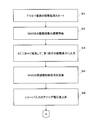
- FIG. 6 to 9 are diagrams illustrating an example of a driver current adjustment processing flow according to the driver output current adjustment method of the present embodiment.
- the output current adjusting device of the driver of this embodiment adjusts the number of NMOS driving stages and drives the PMOS. Adjust the number of steps.
- S2 to S5 in FIG. 6 and S6 to S9 in FIG. 7 show the NMOS drive stage number adjustment processing.
- S10 to S13 in FIG. 8 and S14 to S17 in FIG. 9 show the PMOS drive stage number adjustment processing.
- the driver current controller 12 when the driver current adjustment process starts in S1, the driver current controller 12 starts adjusting the number of NMOS driving stages (S2).
- the driver current controller 12 sets the NMOS stage number control signal N [1] to H, and inputs N [1] to the drive element 111 which is the first stage drive element,
- the NMOS 201 constituting the drive element 111 is turned on (S3).
- the driver current controller 12 further sets N [2] to be input to the drive element 112, which is the second stage drive element, to L, and inputs it to the drive element 113, which is the third stage drive element.
- N [3] is set to L.
- the driver output becomes L by the processing of S3.
- the driver current controller 12 sets the NMOS adjustment control signal to H, transmits the NMOS adjustment control signal to the receiving LSI 2, and turns on the switch 25 (S4).
- the receiving LSI 2 is connected to the pull-up resistor 26 by the process of S4.
- the switch 25 By turning on the switch 25 and connecting the reception LSI 2 to the pull-up resistor 26, the value of the analog voltage at the receiver input increases (S5), and the process proceeds to S6 in FIG.
- the A / D converter 22 converts the analog voltage value of the receiver input into a digital value, and transmits the digital value to the driver current controller 12.
- the driver current controller 12 receives the digital value of the voltage from the A / D converter 22, and determines whether the digital value of the voltage is equal to or less than a predetermined target value (S7).
- the driver current controller 12 determines that the digital value of the voltage is not less than or equal to a predetermined target value
- the driver current controller 12 increases the number of NMOS drive stages (S8) and returns to S6.
- S8 for example, the driver current controller 12 sets the NMOS stage number control signal N [2] to H, inputs N [2] to the second stage driving element, and reduces the number of NMOS driving stages to two. increase.
- the driver current controller 12 increases the number of NMOS driving stages, the driver current increases and the analog voltage at the receiver input decreases.
- the driver current controller 12 determines that the digital value of the voltage is equal to or less than a predetermined target value
- the driver current controller 12 sets the NMOS adjustment control signal to L, and the NMOS adjustment control signal. Is sent to the receiving LSI 2 to turn off the switch 25 (S9).
- the process of adjusting the number of NMOS driving stages is completed by the process of S9, and the process proceeds to S10 of FIG.
- the driver current controller 12 starts adjusting the number of PMOS driving stages.
- the driver current controller 12 sets the PMOS stage number control signal P [1] to H, and inputs P [1] to the driving element 111 which is the first stage driving element,
- the PMOS 200 constituting the drive element 111 is turned on (S11).
- the driver current controller 12 further sets P [2] input to the drive element 112, which is the second stage drive element, to L, and inputs it to the drive element 113, which is the third stage drive element.
- P [3] is set to L.
- the driver output becomes H by the processing of S11.
- the driver current controller 12 sets the PMOS adjustment control signal to H, transmits the PMOS adjustment control signal to the reception LSI 2, and turns on the switch 23 (S12).
- the receiving LSI 2 is connected to the pull-down resistor 24 by the process of S12. As a result, the value of the analog voltage at the receiver input decreases (S13), and the process proceeds to S14 in FIG.
- the A / D converter 22 converts the analog voltage value of the receiver input into a digital value, and transmits the digital value to the driver current controller 12 (S14).
- the driver current controller 12 receives the digital value of the voltage from the A / D converter 22, and determines whether the digital value of the voltage is equal to or greater than a predetermined target value (S15).
- the driver current controller 12 determines that the digital value of the voltage is not greater than or equal to a predetermined target value
- the driver current controller 12 increases the number of PMOS driving stages (S16) and returns to S14.
- the driver current controller 12 sets the PMOS stage number control signal P [2] to H, inputs P [2] to the second stage driving element, and sets the number of PMOS driving stages to two. Increase to.
- the driver current controller 12 increases the number of PMOS driving stages, the driver current increases and the analog voltage at the receiver input increases.
- the driver current controller 12 determines that the digital value of the voltage is equal to or greater than a predetermined target value
- the driver current controller 12 sets the PMOS side adjustment control signal to L and the PMOS side adjustment control signal. Is transmitted to the receiving LSI 2 to turn off the switch 23 (S17). Then, the driver current adjustment process ends (S18).
- the driver current adjustment processing described with reference to FIGS. 6 to 9 separately adjusts the number of PMOS driving stages and the number of NMOS driving stages. Therefore, by adjusting the number of PMOS driving stages, for example, the value of the driver current can be adjusted so that the voltage at the receiver input corresponding to the driver current is equal to or higher than the target value. Further, by adjusting the number of NMOS driving stages, for example, the value of the driver current can be adjusted so that the voltage of the receiver input corresponding to the driver current is equal to or lower than the target value.
- the number of PMOS drive stages or NMOS configuration of the driver is based on the level of the signal corresponding to the value of the current output from the driver. By adjusting the number of drive stages, the current output from the driver can be accurately adjusted.
- the transmission device separately operates the PMOS element and the NMOS element, which are the elements of the driver, according to the level signal indicating the level of the signal received by the reception device from the transmission device. It is possible to switch to
Landscapes
- Engineering & Computer Science (AREA)
- Computer Hardware Design (AREA)
- Physics & Mathematics (AREA)
- Computing Systems (AREA)
- General Engineering & Computer Science (AREA)
- Mathematical Physics (AREA)
- Logic Circuits (AREA)
- Dc Digital Transmission (AREA)
Abstract
Selon l'invention, un pilote (11) émet un courant d'attaque à un circuit de haute intégration (LSI) de réception (2), et un récepteur (21) installé dans le circuit LSI de réception (2) reçoit un signal de tension analogique correspondant à la valeur de courant d'attaque en tant qu'entrée de récepteur. Un convertisseur A/N (22) convertit le signal de tension de l'entrée de récepteur en une valeur numérique et l'envoie à un régulateur de courant d'attaque (12) à l'intérieur d'un circuit LSI d'émission (1). Le régulateur de courant d'attaque (12) commande le nombre d'étages de fonctionnement de PMOS ou NMOS installés dans le pilote (11) de telle manière que la valeur numérique du signal de tension de l'entrée de récepteur peut tomber dans une plage prédéterminée.
Priority Applications (3)
| Application Number | Priority Date | Filing Date | Title |
|---|---|---|---|
| PCT/JP2008/058914 WO2009139057A1 (fr) | 2008-05-15 | 2008-05-15 | Procédé de régulation de courant de sortie de pilote, régulateur de courant de sortie pour pilote et équipement électronique |
| JP2010511819A JP5093346B2 (ja) | 2008-05-15 | 2008-05-15 | ドライバの出力電流調整方法、ドライバの出力電流調整装置及び電子装置 |
| US12/926,229 US8188770B2 (en) | 2008-05-15 | 2010-11-03 | Method and apparatus for adjusting driver output current and electronic apparatus |
Applications Claiming Priority (1)
| Application Number | Priority Date | Filing Date | Title |
|---|---|---|---|
| PCT/JP2008/058914 WO2009139057A1 (fr) | 2008-05-15 | 2008-05-15 | Procédé de régulation de courant de sortie de pilote, régulateur de courant de sortie pour pilote et équipement électronique |
Related Child Applications (1)
| Application Number | Title | Priority Date | Filing Date |
|---|---|---|---|
| US12/926,229 Continuation US8188770B2 (en) | 2008-05-15 | 2010-11-03 | Method and apparatus for adjusting driver output current and electronic apparatus |
Publications (1)
| Publication Number | Publication Date |
|---|---|
| WO2009139057A1 true WO2009139057A1 (fr) | 2009-11-19 |
Family
ID=41318439
Family Applications (1)
| Application Number | Title | Priority Date | Filing Date |
|---|---|---|---|
| PCT/JP2008/058914 Ceased WO2009139057A1 (fr) | 2008-05-15 | 2008-05-15 | Procédé de régulation de courant de sortie de pilote, régulateur de courant de sortie pour pilote et équipement électronique |
Country Status (3)
| Country | Link |
|---|---|
| US (1) | US8188770B2 (fr) |
| JP (1) | JP5093346B2 (fr) |
| WO (1) | WO2009139057A1 (fr) |
Families Citing this family (4)
| Publication number | Priority date | Publication date | Assignee | Title |
|---|---|---|---|---|
| JP5796654B1 (ja) * | 2014-03-27 | 2015-10-21 | 日本電気株式会社 | 信号伝送システム、送信装置、信号伝送方法、および送信装置制御プログラム |
| JP2018019152A (ja) * | 2016-07-26 | 2018-02-01 | ルネサスエレクトロニクス株式会社 | 電源制御コントローラ、半導体装置及び半導体システム |
| CN107634752B (zh) * | 2017-09-20 | 2024-07-16 | 北京集创北方科技股份有限公司 | 驱动装置和驱动方法 |
| KR102679564B1 (ko) | 2019-11-01 | 2024-06-27 | 삼성전자주식회사 | 송신기 회로, 데이터 송신 방법 및 전자 시스템 |
Citations (3)
| Publication number | Priority date | Publication date | Assignee | Title |
|---|---|---|---|---|
| JPH1050070A (ja) * | 1996-08-06 | 1998-02-20 | Nec Niigata Ltd | メモリコントローラ |
| JP2003204258A (ja) * | 2002-01-09 | 2003-07-18 | Toshiba Corp | 半導体装置 |
| WO2004114522A1 (fr) * | 2003-06-24 | 2004-12-29 | Matsushita Electric Industrial Co., Ltd. | Dispositif et procede d'adaptation de l'impedance de sortie dans un systeme d'emission de signaux |
Family Cites Families (6)
| Publication number | Priority date | Publication date | Assignee | Title |
|---|---|---|---|---|
| JP2001339283A (ja) * | 2000-05-26 | 2001-12-07 | Mitsubishi Electric Corp | 遅延回路およびそのための半導体回路装置 |
| JP3520913B2 (ja) * | 2000-06-09 | 2004-04-19 | 日本電気株式会社 | 信号線制御方式 |
| US6861918B2 (en) * | 2002-09-16 | 2005-03-01 | Ene Technology Inc. | Compensation circuit for current control oscillator |
| JP2004114522A (ja) | 2002-09-26 | 2004-04-15 | Fuji Photo Film Co Ltd | 感熱記録材料 |
| US7218168B1 (en) * | 2005-08-24 | 2007-05-15 | Xilinx, Inc. | Linear voltage regulator with dynamically selectable drivers |
| US20070222493A1 (en) * | 2006-03-23 | 2007-09-27 | Sharp Laboratories Of America, Inc. | Digital-to-time converter |
-
2008
- 2008-05-15 WO PCT/JP2008/058914 patent/WO2009139057A1/fr not_active Ceased
- 2008-05-15 JP JP2010511819A patent/JP5093346B2/ja not_active Expired - Fee Related
-
2010
- 2010-11-03 US US12/926,229 patent/US8188770B2/en not_active Expired - Fee Related
Patent Citations (3)
| Publication number | Priority date | Publication date | Assignee | Title |
|---|---|---|---|---|
| JPH1050070A (ja) * | 1996-08-06 | 1998-02-20 | Nec Niigata Ltd | メモリコントローラ |
| JP2003204258A (ja) * | 2002-01-09 | 2003-07-18 | Toshiba Corp | 半導体装置 |
| WO2004114522A1 (fr) * | 2003-06-24 | 2004-12-29 | Matsushita Electric Industrial Co., Ltd. | Dispositif et procede d'adaptation de l'impedance de sortie dans un systeme d'emission de signaux |
Also Published As
| Publication number | Publication date |
|---|---|
| JPWO2009139057A1 (ja) | 2011-09-15 |
| US8188770B2 (en) | 2012-05-29 |
| JP5093346B2 (ja) | 2012-12-12 |
| US20110050291A1 (en) | 2011-03-03 |
Similar Documents
| Publication | Publication Date | Title |
|---|---|---|
| EP1476945B1 (fr) | Procede et dispositif pour produire selectivement une signalisation differentielle et asymetrique a impedance et temps de transition reglables | |
| US7439761B2 (en) | Apparatus and method for controlling a driver strength | |
| US20200280990A1 (en) | Transmitter and communication system | |
| US20160105183A1 (en) | Receiver circuit and signal receiving method thereof | |
| US8587339B2 (en) | Multi-mode driver with multiple transmitter types and method therefor | |
| JP2007124644A (ja) | 電子回路、該電子回路として構成された差分送信機、及び、自己直列終端送信機を形成する方法(振幅制御、プリ・エンファシス制御及びスルー・レート制御のためのセグメント化と振幅精度及び高電圧保護のための電圧調整とを有する自己直列終端シリアル・リンク送信機) | |
| US7088127B2 (en) | Adaptive impedance output driver circuit | |
| US20120056642A1 (en) | Data output circuit | |
| US6194924B1 (en) | Multi-function controlled impedance output driver | |
| JP5093346B2 (ja) | ドライバの出力電流調整方法、ドライバの出力電流調整装置及び電子装置 | |
| US20120032656A1 (en) | Voltage regulator for impedance matching and pre-emphasis, method of regulating voltage for impedance matching and pre-emphasis, voltage mode driver including the voltage regulator, and voltage-mode driver using the method | |
| US8441283B2 (en) | Integrated circuit | |
| US20070075745A1 (en) | Output driver for controlling impedance and intensity of pre-emphasis driver using mode register set | |
| US8324936B2 (en) | Transmitter and receiver of differential current driving mode, and interface system of differential current driving mode including the same | |
| US7639038B2 (en) | Terminating resistance adjusting method, semiconductor integrated circuit and semiconductor device | |
| EP1378997A2 (fr) | Circuit tampon, pouvant ajuster son impédance de sortie en sychronisme avec le signal de donnée | |
| US8085008B2 (en) | System for accounting for switch impendances | |
| CN111510401B (zh) | 用于校准低功率电压模式发射机驱动器阻抗的系统及方法 | |
| US7148725B1 (en) | Voltage clamp | |
| US7768311B2 (en) | Suppressing ringing in high speed CMOS output buffers driving transmission line load | |
| US7339398B2 (en) | Driver impedance control apparatus and system | |
| US9484916B1 (en) | Adaptive on-chip termination circuitry | |
| JP2010212752A (ja) | Lvdsドライバ、lvds回路、lvds回路の抵抗値調整方法および電流値調整方法 | |
| JP2008042901A (ja) | 自動終端回路 | |
| US8638152B2 (en) | Signal transmission circuits |
Legal Events
| Date | Code | Title | Description |
|---|---|---|---|
| 121 | Ep: the epo has been informed by wipo that ep was designated in this application |
Ref document number: 08752774 Country of ref document: EP Kind code of ref document: A1 |
|
| WWE | Wipo information: entry into national phase |
Ref document number: 2010511819 Country of ref document: JP |
|
| NENP | Non-entry into the national phase |
Ref country code: DE |
|
| 122 | Ep: pct application non-entry in european phase |
Ref document number: 08752774 Country of ref document: EP Kind code of ref document: A1 |