WO2009145140A1 - Pile solaire sensibilisée au colorant - Google Patents
Pile solaire sensibilisée au colorant Download PDFInfo
- Publication number
- WO2009145140A1 WO2009145140A1 PCT/JP2009/059518 JP2009059518W WO2009145140A1 WO 2009145140 A1 WO2009145140 A1 WO 2009145140A1 JP 2009059518 W JP2009059518 W JP 2009059518W WO 2009145140 A1 WO2009145140 A1 WO 2009145140A1
- Authority
- WO
- WIPO (PCT)
- Prior art keywords
- group
- dye
- sensitized solar
- solar cell
- electrolyte
- Prior art date
- Legal status (The legal status is an assumption and is not a legal conclusion. Google has not performed a legal analysis and makes no representation as to the accuracy of the status listed.)
- Ceased
Links
Images
Classifications
-
- H—ELECTRICITY
- H01—ELECTRIC ELEMENTS
- H01G—CAPACITORS; CAPACITORS, RECTIFIERS, DETECTORS, SWITCHING DEVICES, LIGHT-SENSITIVE OR TEMPERATURE-SENSITIVE DEVICES OF THE ELECTROLYTIC TYPE
- H01G9/00—Electrolytic capacitors, rectifiers, detectors, switching devices, light-sensitive or temperature-sensitive devices; Processes of their manufacture
- H01G9/20—Light-sensitive devices
- H01G9/2004—Light-sensitive devices characterised by the electrolyte, e.g. comprising an organic electrolyte
-
- H—ELECTRICITY
- H01—ELECTRIC ELEMENTS
- H01G—CAPACITORS; CAPACITORS, RECTIFIERS, DETECTORS, SWITCHING DEVICES, LIGHT-SENSITIVE OR TEMPERATURE-SENSITIVE DEVICES OF THE ELECTROLYTIC TYPE
- H01G9/00—Electrolytic capacitors, rectifiers, detectors, switching devices, light-sensitive or temperature-sensitive devices; Processes of their manufacture
- H01G9/20—Light-sensitive devices
- H01G9/2027—Light-sensitive devices comprising an oxide semiconductor electrode
- H01G9/2031—Light-sensitive devices comprising an oxide semiconductor electrode comprising titanium oxide, e.g. TiO2
-
- H—ELECTRICITY
- H01—ELECTRIC ELEMENTS
- H01G—CAPACITORS; CAPACITORS, RECTIFIERS, DETECTORS, SWITCHING DEVICES, LIGHT-SENSITIVE OR TEMPERATURE-SENSITIVE DEVICES OF THE ELECTROLYTIC TYPE
- H01G9/00—Electrolytic capacitors, rectifiers, detectors, switching devices, light-sensitive or temperature-sensitive devices; Processes of their manufacture
- H01G9/20—Light-sensitive devices
- H01G9/2059—Light-sensitive devices comprising an organic dye as the active light absorbing material, e.g. adsorbed on an electrode or dissolved in solution
-
- Y—GENERAL TAGGING OF NEW TECHNOLOGICAL DEVELOPMENTS; GENERAL TAGGING OF CROSS-SECTIONAL TECHNOLOGIES SPANNING OVER SEVERAL SECTIONS OF THE IPC; TECHNICAL SUBJECTS COVERED BY FORMER USPC CROSS-REFERENCE ART COLLECTIONS [XRACs] AND DIGESTS
- Y02—TECHNOLOGIES OR APPLICATIONS FOR MITIGATION OR ADAPTATION AGAINST CLIMATE CHANGE
- Y02E—REDUCTION OF GREENHOUSE GAS [GHG] EMISSIONS, RELATED TO ENERGY GENERATION, TRANSMISSION OR DISTRIBUTION
- Y02E10/00—Energy generation through renewable energy sources
- Y02E10/50—Photovoltaic [PV] energy
- Y02E10/542—Dye sensitized solar cells
-
- Y—GENERAL TAGGING OF NEW TECHNOLOGICAL DEVELOPMENTS; GENERAL TAGGING OF CROSS-SECTIONAL TECHNOLOGIES SPANNING OVER SEVERAL SECTIONS OF THE IPC; TECHNICAL SUBJECTS COVERED BY FORMER USPC CROSS-REFERENCE ART COLLECTIONS [XRACs] AND DIGESTS
- Y02—TECHNOLOGIES OR APPLICATIONS FOR MITIGATION OR ADAPTATION AGAINST CLIMATE CHANGE
- Y02E—REDUCTION OF GREENHOUSE GAS [GHG] EMISSIONS, RELATED TO ENERGY GENERATION, TRANSMISSION OR DISTRIBUTION
- Y02E10/00—Energy generation through renewable energy sources
- Y02E10/50—Photovoltaic [PV] energy
- Y02E10/549—Organic PV cells
Definitions
- the present invention relates to a dye-sensitized solar cell using, as a charge transfer layer, an electrolyte containing an organic compound that generates a radical compound in at least one of an electrochemical oxidation reaction or a reduction reaction.
- dye-sensitized solar cells can be manufactured in a simple manufacturing process under atmospheric pressure using a general printing process. It is attracting attention as a next-generation solar cell following silicon, polycrystalline silicon, amorphous silicon, CIGS, and the like.
- dye molecules adsorbed on the semiconductor surface absorb sunlight, and electrons are injected from the dye LUMO (lowest orbital) into the semiconductor CB (conduction band), so-called spectral sensitization. I do. Since the dye molecule is bonded to the semiconductor surface via an adsorbing group, it is generally considered to be a monomolecular layer. That is, in order to convert light incident on the solar cell into electrons with high efficiency, a technique for improving the light absorption ability of the dye is required.
- the specific surface area can be increased to several thousand times, and sunlight incident on the solar battery cell can be efficiently converted into electrons.
- the dye absorbs light energy and emits electrons, and the semiconductor titania receives the electrons and delivers them to the conductive substrate.
- the holes remaining in the dye oxidize iodine ions in the electrolyte, I ⁇ changes to I 3 ⁇ , and this oxidized I 3 ⁇ receives and reduces electrons again at the counter electrode, and the electrons cycle through both electrodes. To generate electricity.
- the open-circuit voltage of the dye-sensitized solar cell is defined by the difference between the Fermi level of the oxide semiconductor and the redox potential of the redox in the electrolyte.
- Iodine redox I ⁇ / I 3 ⁇
- Iodine redox is typically used for charge transfer in conventional dye-sensitized solar cells.
- iodine is highly corrosive to metals
- platinum generally used as a counter electrode is known to corrode under high temperature storage.
- non-iodine redox and electrolytes have been studied from the viewpoints of sublimability of iodine itself and loss of conversion efficiency due to a decrease in transmitted light due to coloring.
- bromine redox has been studied as a halogen-based redox similar to iodine redox (for example, see Non-Patent Documents 2 and 3). Since the redox potential of bromine redox is more noble (positive) than iodine redox, the energy level difference of HOMO / LUMO such as coumarin 343 and eosin Y is large, and the organic dye having a shorter absorption region has an open circuit voltage. Improvement is recognized.
- SCN ⁇ / (SCN) 2 or the like As an inorganic redox, SCN ⁇ / (SCN) 2 or the like has been studied, but its performance is inferior to iodine redox (see, for example, Non-Patent Document 4).
- a semiconductor comprising a tetramethylpiperidinyloxy (TEMPO) derivative that generates a radical compound in at least one of an electrochemical oxidation reaction or a reduction reaction, and a dense layer of indium / tin oxide formed by sputtering.
- TEMPO tetramethylpiperidinyloxy
- a photoelectrochemical device composed of a layer and an electrolyte layer has been proposed (see, for example, Patent Document 1), but is not an invention related to a dye-sensitized solar cell, but is related to performance improvement and durability in a dye-sensitized solar cell. No performance improvement is suggested.
- the present invention is to solve the above-described problems, and an object thereof is to provide a dye-sensitized solar cell having a high open-circuit voltage and durability under high-temperature storage.
- the problem of the present invention has been solved by using an electrolyte containing a specific radical compound in producing a dye-sensitized solar cell. Specifically, this was achieved by the following configuration.
- a dye-sensitized solar cell having, on a conductive substrate, a porous n-type semiconductor electrode having a dye adsorbed on its surface, a charge transfer layer, and a counter electrode, wherein the charge transfer layer is an N-oxyl derivative
- a dye-sensitized solar cell comprising a radical compound comprising:
- N-oxyl derivative is an azaadamantane N-oxyl derivative or an azabicyclo N-oxyl derivative.
- R 1 , R 2 , R 3 and R 4 each independently represents a hydrogen atom, an aliphatic hydrocarbon group, an aromatic hydrocarbon group or a heterocyclic group, and X is necessary for forming a cyclic structure. 2 or 3 atomic groups.) 4). 4. The dye-sensitized solar cell according to any one of 1 to 3, wherein the charge transfer layer contains an organic solvent.
- the present invention it is possible to provide a dye-sensitized solar cell that has a high open-circuit voltage and has durability under high-temperature storage.
- the present inventor has investigated dye-sensitized solar cells having a composite electrode, such as open-circuit voltage, short-circuit current, form factor fill factor, photoelectric conversion efficiency, etc., and as a result, dye-sensitized using iodine redox. It was confirmed that the photoelectric conversion efficiency has not yet reached a sufficiently satisfactory level in the type solar cell configuration.
- a dye-sensitized dye having a porous n-type semiconductor electrode having a dye adsorbed on its surface, a charge transfer layer, and a counter electrode in order on a conductive substrate.
- Dye-sensitized solar cell which is characterized in that the charge transfer layer contains the radical compound of the present invention, and not only a high open-circuit voltage can be realized, but also excellent stability during high-temperature storage It is as soon as the present invention has been found out that it has the property.
- N-oxyl also called nitroxide radical
- N-oxyl is an oxygen-centered radical generated by radically cleaving the oxygen-hydrogen bond of hydroxylamine.
- compounds having> NO structure in the molecule are generically called N-oxyl derivatives.
- N-oxyl derivatives are more stable than other radical compounds and can be extracted as crystals.
- N-oxyl derivatives derivatives substituted with various substituents such as TEMPO (2,2,6,6-tetramethylpiperidinyl-N-oxyl) are commercially available.
- the four methyl groups substituted at the N-oxyl group ⁇ -position of TEMPO are important structural chemical elements when present as stable radicals.
- N-oxyl derivative When an N-oxyl derivative is used as a redox couple in a dye-sensitized solar cell, the stability of the compound itself is important for enhancing the durability of the battery. Therefore, a compound in which no hydrogen is substituted on the ⁇ -position carbon of the N-oxyl group is preferable.
- the TEMPO derivative may be less reactive due to steric hindrance of the four methyl groups.
- An azaadamantane N-oxyl derivative or an azabicyclo N-oxyl derivative is more preferable in that it does not cause such a decrease in activity.
- the Bredt rule prevents isomerization to nitrone and ensures the existence as a stable radical.
- These azaadamantane N-oxyl derivatives or azabicyclo N-oxyl derivatives may have a substituent at a substitutable position, and a large amount such as a dimer, a trimer or the like can be obtained by using these substituents as a linking group. It may form a body or may be a polymer.
- the most preferred N-oxyl derivative is an azaadamantane N-oxyl derivative or an azabicyclo N-oxyl derivative represented by the general formula (1).
- R 1 , R 2 , R 3 and R 4 each independently represent a hydrogen atom, an aliphatic hydrocarbon group, an aromatic hydrocarbon group or a heterocyclic group, and an aliphatic hydrocarbon group ,
- the aromatic hydrocarbon group and the heterocyclic group may have a substituent.
- X represents a group of 2 or 3 atoms necessary for forming a cyclic structure. Specific examples include CH 2 , CO, and C having a substituent.
- the aliphatic hydrocarbon group includes chain and cyclic groups, and the chain group includes linear and branched groups.
- Such aliphatic hydrocarbon groups include methyl, ethyl, vinyl, propyl, isopropyl, propenyl, butyl, iso-butyl, t-butyl, pentyl, isopentyl, neopentyl, hexyl, iso-hexyl, cyclohexyl, cyclohexenyl, Examples include octyl, iso-octyl, cyclooctyl, 2,3-dimethyl-2-butyl and the like.
- Examples of the aromatic hydrocarbon group include a phenyl group and a naphthyl group.
- Examples of the heterocyclic group include a pyridyl group, a thiazolyl group, an oxazolyl group, an imidazolyl group, a furyl group, a pyrrolyl group, a pyrazinyl group, a pyrimidinyl group, and a pyridazinyl group.
- substituents may further have a substituent.
- substituents are not particularly limited, and examples thereof include alkyl groups (for example, methyl group, ethyl group, propyl group, isopropyl group, t-butyl group, pentyl group, hexyl group, octyl group, dodecyl group, tridecyl group, Tetradecyl group, pentadecyl group etc.), cycloalkyl group (eg cyclopropyl group, cyclopentyl group, cyclohexyl group etc.), alkenyl group (eg vinyl group, allyl group, butenyl group, octenyl group etc.), cycloalkenyl group (eg 2-cyclopenten-1-yl group, 2-cyclohexen-1-yl group, etc.), alkynyl group (eg, propargyl group, ethynyl group, trimethylsilylethy
- the compound represented by the general formula (1) may be a multimer such as a dimer or a trimer linked by these substituents, or may be a polymer.
- the charge transfer layer constituting the dye-sensitized solar cell of the present invention is a layer containing a charge transport material having a function of replenishing electrons to the oxidant of the dye.
- typical charge transport materials include a solvent in which a redox counter ion is dissolved, an electrolyte such as a room temperature molten salt containing the redox counter ion, and a solution of the redox counter ion as a polymer matrix. And a gel-like quasi-solidified electrolyte impregnated with a low-molecular gelling agent, and a polymer solid electrolyte.
- electron transport materials and hole transport materials can also be used as materials in which carrier transport in solids is involved in electrical conduction, and these can be used in combination. is there.
- a solvent As a solvent, it is an electrochemically inert compound that has low viscosity and improved ion mobility, or has a high dielectric constant and improved effective carrier concentration, and can exhibit excellent ionic conductivity. Is desirable.
- carbonate compounds such as dimethyl carbonate, diethyl carbonate, ethylene carbonate and propylene carbonate, heterocyclic compounds such as 3-methyl-2-oxazolidinone, ether compounds such as dioxane and diethyl ether, ethylene glycol dialkyl ether, propylene glycol Chain ethers such as dialkyl ether, polyethylene glycol dialkyl ether, polypropylene glycol dialkyl ether, alcohols such as methanol, ethanol, ethylene glycol monoalkyl ether, propylene glycol monoalkyl ether, polyethylene glycol monoalkyl ether, polypropylene glycol monoalkyl ether , Ethylene glycol, diethylene glycol, trie Polyhydric alcohols such as lenglycol, polyethylene glycol, propylene glycol, polypropylene glycol, glycerin, nitrile compounds such as acetonitrile, glutarodinitrile, propionitrile, methoxypropion
- the solvent preferably has a boiling point of 80 ° C. or higher, more preferably 100 ° C. or higher, and still more preferably 120 ° C. or higher from the viewpoint of durability.
- Specific examples include 3-methoxypropionitrile (165 ° C.), ethylene carbonate (243 ° C.), propylene carbonate (240 ° C.), and ⁇ -butyrolactone (203 ° C.).
- a preferable electrolyte concentration is 0.1 to 15 mol / L, and more preferably 0.2 to 10 mol / L.
- the molten salt electrolyte is preferable from the viewpoint of achieving both photoelectric conversion efficiency and durability.
- the molten salt electrolyte for example, International Publication No. 95/18456 pamphlet, JP-A-8-259543, JP-A-2001-357896, Electrochemistry, Vol. 65, No. 11, page 923 (1997).
- electrolytes such as pyridinium salts, imidazolium salts, and triazolium salts described in the above. These molten salt electrolytes are preferably in a molten state at room temperature, and it is preferable not to use a solvent.
- polyacrylonitrile and polyvinylidene fluoride can be preferably used.
- a preferred compound is a compound having an amide structure in the molecular structure.
- a polymer containing a crosslinkable reactive group and a crosslinking agent in combination.
- a preferable crosslinkable reactive group is a nitrogen-containing heterocyclic ring (for example, a pyridine ring, an imidazole ring, a thiazole ring, an oxazole ring, a triazole ring, a morpholine ring, a piperidine ring, a piperazine ring, etc.), and a preferable crosslinking agent is It is a reagent (for example, alkyl halide, halogenated aralkyl, sulfonic acid ester, acid anhydride, acid chloride, isocyanate, etc.) capable of electrophilic reaction with a nitrogen atom.
- the concentration of the electrolyte is usually 0.01 to 99% by mass, preferably about 0.1 to 90% by mass.
- an electrolyte composition containing an electrolyte and metal oxide particles and / or conductive particles can also be used.
- the metal oxide particles TiO 2 , SnO 2 , WO 3 , ZnO, ITO, BaTiO 3 , Nb 2 O 5 , In 2 O 3 , ZrO 2 , Ta 2 O 5 , La 2 O 3 , SrTiO 3 , Y
- examples thereof include one or a mixture of two or more selected from the group consisting of 2 O 3 , Ho 2 O 3 , Bi 2 O 3 , CeO 2 , and Al 2 O 3 . These may be doped with impurities or complex oxides.
- the conductive particles include those made of a substance mainly composed of carbon.
- the polymer electrolyte is a solid substance capable of dissolving the redox species or binding with at least one substance constituting the redox species, for example, polyethylene oxide, polypropylene oxide, polyethylene succinate, Polyethers to polymer functional groups such as poly- ⁇ -propiolactone, polyethyleneimine, polyalkylene sulfide and the like, or cross-linked products thereof, polyphosphazene, polysiloxane, polyvinyl alcohol, polyacrylic acid, polyalkylene oxide, etc. Examples include those obtained by adding segments or oligoalkylene oxide structures as side chains, or copolymers thereof. Among them, those having oligoalkylene oxide structures as side chains, and polyether segments as side chains. Which is preferable.
- a method of polymerizing in the coexistence of a monomer that becomes a polymer compound and a redox species a solid such as a polymer compound is dissolved in a solvent as necessary. Then, the above-mentioned method of adding the redox species can be used.
- the content of the redox species can be appropriately selected according to the required ion conduction performance.
- a solid hole transport material which is organic or inorganic or a combination of both can be used.
- Organic hole transport materials include aromatic amines and triphenylene derivatives, polyacetylene and derivatives thereof, poly (p-phenylene) and derivatives thereof, poly (p-phenylene vinylene) and derivatives thereof, polythienylene vinylene and derivatives thereof.
- Conductive polymers such as derivatives, polythiophene and derivatives thereof, polyaniline and derivatives thereof, polytoluidine and derivatives thereof can be preferably used.
- the hole transport material may be added with a compound containing a cation radical such as tris (4-bromophenyl) aminium hexachloroantimonate, or the potential of the oxide semiconductor surface.
- a salt such as Li [(CF 3 SO 2 ) 2 N] may be added.
- the inorganic hole transport material a p-type inorganic compound semiconductor can be used.
- the p-type inorganic compound semiconductor for this purpose preferably has a band gap of 2 eV or more, and more preferably 2.5 eV or more.
- the ionization potential of the p-type inorganic compound semiconductor needs to be smaller than the ionization potential of the dye-adsorbing electrode from the condition that the holes of the dye can be reduced.
- the preferred range of the ionization potential of the p-type inorganic compound semiconductor varies depending on the dye used, it is generally preferably 4.5 to 5.5 eV, more preferably 4.7 to 5.3 eV.
- a preferred p-type inorganic compound semiconductor is a compound semiconductor containing monovalent copper, preferably CuI and CuSCN, and most preferably CuI.
- the preferred hole mobility of the charge transfer layer containing the p-type inorganic compound semiconductor is 1 ⁇ 10 ⁇ 4 to 1 ⁇ 10 4 m 2 / V ⁇ sec, more preferably 1 ⁇ 10 ⁇ 3 to 1 ⁇ 10 3 cm. 2 / V ⁇ sec.
- the preferred conductivity of the charge transport layer is 1 ⁇ 10 ⁇ 8 to 1 ⁇ 10 2 S / cm, more preferably 1 ⁇ 10 ⁇ 6 to 10 S / cm.
- the method for forming the charge transfer layer between the porous n-type semiconductor electrode and the counter electrode is not particularly limited.
- the porous n-type semiconductor electrode and the counter electrode are arranged to face each other.
- the charge transfer layer is formed by filling the above-described electrolyte or various electrolytes between both electrodes to form a charge transfer layer, or by dropping or coating the electrolyte or various electrolytes on the porous n-type semiconductor electrode or the counter electrode.
- a method of superimposing the other electrode on the charge transfer layer can be used.
- sealing is performed using a film or a resin in the gap between the porous n-type semiconductor electrode and the counter electrode as necessary. It is also preferable to store the porous n-type semiconductor electrode, the charge transfer layer, and the counter electrode in an appropriate case.
- a normal pressure process using capillary action by dipping or the like, or a vacuum process in which the gas phase in the gap is replaced with a liquid phase at a pressure lower than normal pressure can be used.
- microgravure coating, dip coating, screen coating, spin coating or the like can be used as a coating method.
- the counter electrode is provided in an undried state and measures for preventing liquid leakage at the edge portion are taken.
- a gel electrolyte there is a method in which it is applied in a wet manner and solidified by a method such as polymerization. In this case, the counter electrode can be applied after drying and fixing.
- a charge transfer layer can be formed by a dry film formation process such as a vacuum deposition method or a CVD method, and then a counter electrode can be provided. Specifically, it can be introduced into the electrode by techniques such as vacuum deposition, casting, coating, spin coating, dipping, electropolymerization, and photoelectropolymerization. It is formed by evaporating the solvent by heating to an arbitrary temperature.
- the thickness of the charge transfer layer is preferably 10 ⁇ m or less, more preferably 5 ⁇ m or less, and further preferably 1 ⁇ m or less.
- the electric conductivity of the charge transfer layer is preferably 1 ⁇ 10 ⁇ 10 S / cm or more, and more preferably 1 ⁇ 10 ⁇ 5 S / cm or more.
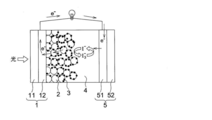
- FIG. 1 is a schematic cross-sectional view showing the basic structure of the dye-sensitized solar cell of the present invention.
- the dye-sensitized solar cell of the present invention includes a conductive substrate 1, a porous n-type semiconductor electrode 2 having a dye 3 adsorbed on the surface of a semiconductor, and a charge transfer layer (“electrolyte”). 4) and a counter electrode 5 (sometimes referred to as a “layer”).
- e ⁇ represents an electron
- an arrow represents the flow of the electron.
- the porous n-type semiconductor electrode, the charge transfer layer and the counter electrode are housed in a case and sealed, or the whole is sealed with resin. It is preferable.
- the dye-sensitized solar cell of the present invention When the dye-sensitized solar cell of the present invention is irradiated with sunlight or an electromagnetic wave equivalent to sunlight, the dye 3 adsorbed on the semiconductor is excited by absorbing the irradiated sunlight or electromagnetic wave. Electrons generated by excitation move to the semiconductor, and then move to the counter electrode 5 via the conductive substrate 1 to reduce the redox electrolyte of the charge transfer layer 4.
- the dye 3 that has moved electrons to the semiconductor is an oxidant, but is reduced to the original state by supplying electrons from the counter electrode 5 via the redox electrolyte of the charge transfer layer 4.
- the iodine redox (in the present invention, the radical compound according to the present invention) of the charge transfer layer 4 is oxidized and returns to a state where it can be reduced again by the electrons supplied from the counter electrode 5. In this way, electrons flow and the dye-sensitized solar cell of the present invention can be configured.
- Metal oxide semiconductor layer ⁇ Metal oxide semiconductor layer ⁇ The metal oxide semiconductor layer according to the present invention will be described.
- the metal oxide constituting the metal oxide semiconductor layer according to the present invention is not particularly limited as long as it is a semiconductor that receives electrons generated by light irradiation with a dye adsorbed on the semiconductor and transmits the electrons to a conductive substrate.
- Various metal oxides used in the dye-sensitized solar cell can be used.
- various metal oxide semiconductors such as titanium oxide, zirconium oxide, zinc oxide, vanadium oxide, niobium oxide, tantalum oxide, tungsten oxide, strontium titanate, calcium titanate, magnesium titanate, barium titanate, niobium
- metal oxide semiconductors such as potassium oxide and strontium tantalate, transition metal oxides such as magnesium oxide, strontium oxide, aluminum oxide, cobalt oxide, nickel oxide and manganese oxide, cerium oxide, gadolinium oxide, samarium oxide, ytterbium oxide And metal oxides such as lanthanoid oxides, and inorganic insulators such as natural or synthetic silicate compounds represented by silica.
- the metal oxide particles may have a core-shell structure or may be doped with a different metal element, and a metal oxide having an arbitrary structure and composition can be applied.
- the average particle diameter of the metal oxide particles is preferably from 10 nm to 300 nm, more preferably from 10 nm to 100 nm.
- the shape of the metal oxide is not particularly limited, and may be spherical, acicular or amorphous crystals.
- the method for forming metal oxide particles is not particularly limited, and various liquid phase methods such as hydrothermal reaction method, sol-gel method / gel sol method, colloid chemical synthesis method, coating pyrolysis method, spray pyrolysis method, and chemical vapor phase It can be formed using various gas phase methods such as a precipitation method.
- a known method can be applied, and (1) a suspension containing metal oxide fine particles or a precursor thereof.
- a method of forming a semiconductor layer by applying a liquid on a conductive substrate, drying and baking, and (2) immersing the conductive substrate in a colloidal solution and conducting the metal oxide semiconductor particles by electrophoresis.
- Electrophoretic electrodeposition method that adheres to a conductive substrate, (3) A method in which a foaming agent is mixed and applied to a colloidal solution or dispersion, and then sintered to make it porous.
- a polymer microbead is mixed. After the coating, a method of removing the polymer microbeads by heat treatment or chemical treatment to form voids and making it porous can be applied.
- a coating method a known method can be applied, and examples thereof include a screen printing method, an ink jet method, a roll coating method, a doctor blade method, a spin coating method, and a spray coating method. Can do.
- the particle diameter of the metal oxide fine particles in the suspension is preferably fine and is preferably present as primary particles.
- the suspension containing the metal oxide fine particles is prepared by dispersing the metal oxide fine particles in a solvent, and the solvent is not particularly limited as long as the metal oxide fine particles can be dispersed, and water, Organic solvents, mixtures of water and organic solvents are included.
- the organic solvent alcohols such as methanol and ethanol, ketones such as methyl ethyl ketone, acetone and acetyl acetone, hydrocarbons such as hexane and cyclohexane, and the like are used.
- a surfactant and a viscosity modifier can be added to the suspension as necessary.
- concentration range of the metal oxide fine particles in the solvent is preferably 0.1 to 70% by mass, and more preferably 0.1 to 30% by mass.
- the suspension containing the metal oxide core fine particles obtained as described above is applied onto a conductive substrate, dried, etc., and then baked in air or in an inert gas to be conductive.
- a metal oxide semiconductor layer is formed on the conductive substrate.
- the semiconductor layer obtained by applying and drying the suspension on the conductive substrate is composed of an aggregate of metal oxide fine particles, and the particle size of the fine particles corresponds to the primary particle size of the metal oxide fine particles used. To do.
- the body film is preferably fired to increase the mechanical strength, and is preferably a fired product film that is strongly fixed to the substrate.
- the metal oxide semiconductor layer may have any structure, but is preferably a porous structure film (also referred to as a porous layer having voids).
- the porosity of the metal oxide semiconductor layer is preferably 0.1 to 20% by volume, and more preferably 5 to 20% by volume.
- the porosity of the metal oxide semiconductor layer means a porosity that is penetrable in the thickness direction of the dielectric, and can be measured using a commercially available apparatus such as a mercury porosimeter (Shimadzu Polarizer 9220 type).
- the thickness of the metal oxide semiconductor layer is preferably at least 10 nm or more, and more preferably 100 to 10,000 nm.
- the actual surface area of the semiconductor layer is appropriately adjusted, and the firing temperature is preferably lower than 1000 ° C., more preferably in the range of 200 to 800 ° C. from the viewpoint of obtaining a semiconductor layer having the above porosity. .
- the metal oxide semiconductor layer is formed on the metal oxide intermediate layer as described above, the metal oxide semiconductor layer is formed on the metal oxide semiconductor film as necessary for the purpose of improving electronic conductivity. You may perform the surface treatment by a metal oxide.
- the surface treatment composition is preferably the same type of composition as that of the metal oxide forming the metal oxide semiconductor layer, particularly from the viewpoint of electron conductivity between the metal oxide fine particles.
- a metal oxide precursor to be surface treated is applied to the semiconductor film, or the semiconductor film is a precursor.
- a surface treatment made of a metal oxide can be performed by immersing in a body solution and further performing a firing treatment as necessary.
- the surface treatment is performed by using an electrochemical treatment using a titanium tetrachloride aqueous solution or titanium alkoxide which is a precursor of titanium oxide, or using a precursor of an alkali metal titanate or an alkaline earth titanate metal.
- the firing temperature and firing time at this time are not particularly limited and can be arbitrarily controlled, but are preferably 200 ° C. or lower.
- the conductive substrate is preferably substantially transparent when the light-receiving surface is the conductive substrate side of the dye-sensitized solar cell. “Substantially transparent” means that the light transmittance is 10% or more, preferably 50% or more, and particularly preferably 80% or more.
- a substrate having conductivity by itself or a substrate having a conductive layer on the surface thereof can be used.
- a glass plate, a ceramic polishing plate such as titanium oxide or alumina, and various known plastic sheets as the base material it is possible to use a glass plate, a ceramic polishing plate such as titanium oxide or alumina, and various known plastic sheets as the base material, but considering the cost and flexibility, plastic It is preferable to use a sheet.
- plastic sheet examples include triacetyl cellulose (TAC), polyethylene terephthalate (PET), polyethylene naphthalate (PEN), polyphenylene sulfide (PPS), syndiotactic polyester (SPS), and polycarbonate (PC).
- TAC triacetyl cellulose
- PET polyethylene terephthalate
- PEN polyethylene naphthalate
- PPS polyphenylene sulfide
- SPS syndiotactic polyester
- PC polycarbonate
- PA Polyarylate
- PEI polyetherimide
- PSF polysulfone
- PES polyethersulfone
- cyclic polyolefin phenoxy resin
- brominated phenoxy and the like examples of the plastic sheet.
- Examples of the conductive material used for the conductive layer provided on these substrates include inorganic conductive materials made of various known metals and metal oxides, polymer conductive materials, and inorganic / organic composite conductive materials. Or any material such as a conductive material in which these are arbitrarily mixed can be used.
- the inorganic conductive material include metals such as platinum, gold, silver, copper, zinc, titanium, aluminum, rhodium, and indium, conductive carbon, tin-doped indium oxide (ITO), and tin oxide (SnO 2 ). And metal oxides such as fluorine-doped tin oxide (FTO), antimony-doped tin oxide (ATO), and zinc oxide (ZnO 2 ).
- metals such as platinum, gold, silver, copper, zinc, titanium, aluminum, rhodium, and indium
- conductive carbon tin-doped indium oxide (ITO), and tin oxide (SnO 2 ).
- ITO tin-doped indium oxide
- SnO 2 tin oxide
- metal oxides such as fluorine-doped tin oxide (FTO), antimony-doped tin oxide (ATO), and zinc oxide (ZnO 2 ).
- polymer-based conductive material examples include conductive polymers obtained by polymerizing thiophene, pyrrole, furan, aniline, etc., which may or may not be variously substituted, and polyacetylene. From the viewpoint of high properties, polythiophene is preferable, and polyethylenedioxythiophene (PEDOT) is particularly preferable.
- PEDOT polyethylenedioxythiophene
- a known appropriate method according to a conductive material can be used. For example, when forming a conductive layer made of a metal oxide such as ITO, a sputtering method is used. And thin film forming methods such as CVD, SPD (spray pyrolysis deposition), and vapor deposition. Further, when forming a conductive layer made of a polymer-based conductive material, it is preferably formed by various known coating methods.
- the thickness of the conductive layer is preferably about 0.01 to 10 ⁇ m, more preferably about 0.05 to 5 ⁇ m.
- a conductive base material the lower the surface resistance, the better. Specifically, it is preferably 50 ⁇ / cm 2 or less, more preferably 10 ⁇ / cm 2 or less.
- a metal wiring layer made of tungsten or the like may be used in combination with the conductive layer.
- a metal wiring layer it is preferable to install the conductive layer on the substrate by vapor deposition, sputtering, or the like.
- a short-circuit prevention layer can be provided between the conductive layer and the metal oxide semiconductor electrode described above. Thereby, the short circuit current of electrolyte and a metal oxide semiconductor can be reduced.
- a solid p-type semiconductor is used as the electrolyte, it is preferable to have this layer.
- the short-circuit preventing layer is not particularly limited as long as it is an n-type semiconductor that is an insulating substance that transmits visible light and has a conduction band energy level close to that of a metal oxide semiconductor.
- silicon oxide, magnesium oxide, aluminum oxide, calcium carbonate, polyvinyl alcohol, polyurethane and the like can be mentioned.
- a photoelectric conversion material may be used, for example, titanium oxide, niobium oxide, tungsten oxide, etc. are mentioned.
- the short-circuit prevention layer As a method for forming the short-circuit prevention layer, it can be produced by a vacuum film formation process, a liquid phase coating method, or the like, as in the case of the transparent conductive layer.
- the transparent conductive layer, the short-circuit prevention layer, and the metal oxide film can be formed in-line under vacuum without being exposed to the atmosphere.
- the film thickness of the short-circuit prevention layer is preferably 0.001 to 0.02 ⁇ m, but can be adjusted as appropriate.
- the dye adsorbed on the surface of the porous n-type semiconductor electrode 2 shown in FIG. 1 has absorption in various visible light regions and / or infrared light regions, and is a metal oxide semiconductor.
- a dye having the lowest vacancy level higher than the conduction band is preferable, and various known dyes can be used.
- azo dyes for example, azo dyes, quinone dyes, quinone imine dyes, quinacridone dyes, squarylium dyes, cyanine dyes, cyanidin dyes, merocyanine dyes, triphenylmethane dyes, xanthene dyes, porphyrin dyes, perylene dyes And dyes, indigo dyes, phthalocyanine dyes, naphthalocyanine dyes, rhodamine dyes, and the like.
- Metal complex dyes are also preferably used.
- Various metals such as Tc, Te, and Rh can be used.
- polymethine dyes such as cyanine dyes, merocyanine dyes and squarylium dyes are one of preferred embodiments.
- Examples thereof include dyes described in each specification such as Gazette, European Patent Nos. 892,411 and 911,841.
- a metal complex dye is one of the preferred embodiments, and a metal phthalocyanine dye, a metal porphyrin dye or a ruthenium complex dye is preferable, and a ruthenium complex dye is more preferable.
- ruthenium complex dyes include U.S. Pat. Nos. 4,927,721, 4,684,537, 5,084,365, 5,350,644, 5,463,057, Nos. 5,525,440, JP-A-7-249790, JP-A-10-504512, WO98 / 50393, JP2000-26487, 2001-2223037 And complex dyes described in JP-A Nos. 2001-226607 and 3430254.
- the above-mentioned compound according to the present invention is, for example, “Cyanine Soybean and Related Compounds” (1964, published by Inter Science Publishers) by F. M. Hammer, US Pat. No. 2,454,629, It can be synthesized with reference to the methods described in the specifications of JP-A-2,493,748, JP-A-6-301136, JP-A-2003-203684, and the like.
- the dye preferably have a large extinction coefficient and are stable against repeated redox.
- the dye is preferably chemically adsorbed on the metal oxide semiconductor and has a functional group such as a carboxyl group, a sulfonic acid group, a phosphoric acid group, an amide group, an amino group, a carbonyl group, or a phosphine group. preferable.
- two or more kinds of dyes can be used together or mixed.
- the dye used together or mixed and the ratio thereof can be selected so as to match the wavelength range and intensity distribution of the target light source.
- the method for adsorbing the dye to the metal oxide semiconductor layer is not particularly limited, and a known method can be used.
- a method of dissolving a pigment in an organic solvent to prepare a pigment solution and immersing the semiconductor layer on the transparent conductive film in the obtained pigment solution or a method of applying the obtained pigment solution to the surface of the semiconductor layer, etc. Can be mentioned.
- a dip method, a roller method, an air knife method or the like can be applied
- a wire bar method, an application method, a spin method, a spray method, an offset printing method, a screen printing method, or the like can be applied.
- the surface of the semiconductor layer may be subjected to a treatment such as a decompression treatment or a heat treatment in advance to activate the surface and remove bubbles in the film.
- the time for immersing the semiconductor film in the dye solution is preferably 3 to 48 hours, and more preferably 4 to 24 hours.
- the dye solution may be heated to a temperature that does not boil as long as the dye does not decompose.
- the preferred temperature range is 10 to 50 ° C., particularly preferably 15 to 35 ° C., but this is not the case when the solvent boils in the temperature range as described above.
- ultrasonic irradiation can be performed on the dye solution in which the semiconductor film is immersed.
- a commercially available apparatus can be used for ultrasonic irradiation, and the irradiation time is preferably 30 minutes to 4 hours, more preferably 1 to 3 hours.
- the solvent used in the dye solution may be any solvent that dissolves the dye, and a conventionally known solvent can be used.
- the solvent is preferably a solvent purified in accordance with a conventional method, or prior to use of the solvent, distilled and / or dried as necessary, and a higher purity solvent, for example, methanol, ethanol, Butanol, one or more hydrophobic solvents, aprotic solvents, hydrophobic and aprotic solvents or mixtures thereof.
- examples of the hydrophobic solvent include halogenated aliphatic hydrocarbons such as methylene chloride, chloroform and carbon tetrachloride; hydrocarbons such as hexane and cyclohexane; aromatic hydrocarbons such as benzene, toluene and xylene; chlorobenzene, And halogenated aromatic hydrocarbons such as dichlorobenzene; esters such as ethyl acetate, butyl acetate, and ethyl benzoate;
- aprotic solvent examples include ketones such as acetone and methyl ethyl ketone; ethers such as diethyl ether, diisopropyl ether and dimethoxyethane; nitrogen compounds such as acetonitrile, dimethylacetamide and hexamethylphosphoric triamide; carbon disulfide; Sulfur compounds such as dimethyl sulfoxide; phosphorus compounds such as hexamethylphosphoramide; and combinations thereof.
- ketones such as acetone and methyl ethyl ketone
- ethers such as diethyl ether, diisopropyl ether and dimethoxyethane
- nitrogen compounds such as acetonitrile, dimethylacetamide and hexamethylphosphoric triamide
- carbon disulfide Sulfur compounds such as dimethyl sulfoxide
- phosphorus compounds such as hexamethylphosphoramide
- Solvents preferably used include alcohol solvents such as methanol, ethanol, n-propanol and butanol, ketone solvents such as acetone and methyl ethyl ketone, ether solvents such as diethyl ether, diisopropyl ether, tetrahydrofuran and 1,4-dioxane, methylene chloride 1,1,2-trichloroethane and the like, particularly preferably methanol, ethanol, acetone, methyl ethyl ketone, tetrahydrofuran and methylene chloride.
- alcohol solvents such as methanol, ethanol, n-propanol and butanol
- ketone solvents such as acetone and methyl ethyl ketone
- ether solvents such as diethyl ether, diisopropyl ether, tetrahydrofuran and 1,4-dioxane
- the concentration of the dye in the dye solution can be appropriately adjusted depending on the dye used, the type of solvent, and the dye adsorption step. For example, it is 1 ⁇ 10 ⁇ 5 mol / L or more, preferably 5 ⁇ 10 ⁇ 5 to 1 ⁇ . About 10 ⁇ 2 mol / L.
- the sensitization effect becomes insufficient. Conversely, if the adsorption amount is large, the dye that is not adsorbed on the oxide semiconductor floats, which reduces the sensitization effect and reduces the photoelectric conversion efficiency. This is not preferable because it causes a decrease. From the above, it is preferable to quickly remove the unadsorbed dye by washing.
- the washing solvent a solvent such as acetone having a relatively low solubility of the dye and relatively easy to dry is preferable. Moreover, it is preferable to perform washing in a heated state.
- the surface of the oxide semiconductor fine particles may be treated with an organic basic compound in order to make the adsorption state of the dye more stable, thereby promoting the removal of the unreacted dye.
- the organic basic compound include derivatives such as pyridine and quinoline. When these compounds are liquid, they may be used as they are, but when they are solid, they may be dissolved in a solvent, preferably the same solvent as the dye solution.
- the ratio of the dyes to be mixed is not particularly limited, and is selected and optimized from the respective dyes. Generally, about 10% mol or more per one dye is used after mixing in equimolar amounts. It is preferable to do this.
- the dyes may be adsorbed on the semiconductor layer sequentially by mixing and dissolving them.
- the total concentration of the dye in the solution may be the same as when only one kind is supported.
- the above-mentioned solvents can be used. Even when a solution is prepared for each dye to be used in combination and adsorbed to the semiconductor layer, the solvent described above can be used as the solvent, and the solvent for each dye to be used may be the same or different.
- the dye When the dye is supported on the thin film of oxide semiconductor fine particles, it is effective to support the dye in the coexistence of the inclusion compound in order to prevent the association between the dyes.
- the inclusion compound include steroidal compounds such as cholic acid, crown ether, cyclodextrin, calixarene, polyethylene oxide, and the like. Deoxycholic acid, dehydrodeoxycholic acid, chenodeoxycholic acid, cholic acid are preferable. Examples thereof include cholic acids such as methyl ester and sodium cholate, and polyethylene oxide.
- the surface of the semiconductor layer may be treated with an amine compound such as 4-t-butylpyridine.
- the treatment method may be, for example, a method of immersing a substrate provided with a semiconductor fine particle thin film carrying a dye in an ethanol solution of amine.
- the counter electrode constituting the dye-sensitized solar cell of the present invention has a single-layer structure of a base material having conductivity as in the case of the conductive base material described above, or a base material having a counter electrode conductive layer on the surface thereof. Can be used. In the latter case, the conductive material and the base material used for the counter electrode conductive layer, and the manufacturing method thereof are the same as those of the conductive base material 1 described above, and various known materials and methods can be applied.
- I 3 - is preferable to use those having a catalytic ability to perform a reducing reaction fast enough for oxidation and other redox ions such as ions, specifically platinum electrodes, the conductive material surface
- examples include platinum-plated or platinum-deposited materials, rhodium metal, ruthenium metal, ruthenium oxide, and carbon.
- the thickness of the counter electrode conductive layer is not particularly limited, but is preferably 3 nm to 10 ⁇ m.
- the thickness is preferably 5 ⁇ m or less, and more preferably in the range of 10 nm to 3 ⁇ m.
- the surface resistance of the counter electrode is preferably as low as possible. Specifically, the range of the surface resistance is preferably 50 ⁇ / ⁇ or less, more preferably 20 ⁇ / ⁇ or less, still more preferably 10 ⁇ / ⁇ or less. .
- the counter electrode Since light may be received from either one or both of the conductive base material and the counter electrode described above, it is sufficient that at least one of the conductive base material and the counter electrode is substantially transparent. From the viewpoint of improving the power generation efficiency, it is preferable to make the conductive base material transparent so that light is incident from the conductive base material side.
- the counter electrode preferably has a property of reflecting light. As such a counter electrode, glass or plastic deposited with a metal or a conductive oxide, or a metal thin film can be used.
- the counter electrode is formed by directly applying a conductive material on the above-described charge transfer layer, plating or vapor deposition (for example, PVD, CVD), or a conductive layer side of a substrate having a counter electrode conductive layer or a conductive substrate single layer. Just paste.
- a metal wiring layer in combination when the counter electrode is transparent.
- the counter electrode is preferably conductive and has a catalytic action on the reduction reaction of the redox electrolyte.
- a method of depositing platinum, carbon, rhodium, ruthenium or the like on glass or a polymer film, a method of applying conductive fine particles, or the like can be applied.
- Example 1 Preparation of electrolyte L-01 >> Using acetonitrile as a solvent, lithium iodide, iodine, 1,2-dimethyl-3-propylimidazolium iodide, and t-butylpyridine, each at a concentration of 0.1 mol / L, 0.05 mol / L, An iodine redox electrolyte L-01 dissolved at 0.6 mol / L and 0.5 mol / L was prepared.
- a TiO 2 paste (Solaronix Ti-Nanoxide T) is dried at room temperature so that the dry film thickness becomes 10 ⁇ m on the FTO surface of an FTO glass substrate having a surface resistance of 10 ⁇ / ⁇ to be a transparent conductive substrate, and further at 450 ° C. for 30 minutes.
- a porous metal oxide semiconductor layer was formed by performing a sintering process for a minute.
- a cathode electrode platinum was vacuum-deposited on an ITO glass substrate, and a hole for injecting an electrolyte was provided.
- the glass substrate and the cathode electrode are bonded to each other by using a 25 ⁇ m thick sheet-like spacer / sealing material (SX-1170-25, manufactured by Solaronix) having a 6.5 mm square hole, and provided on the cathode electrode.
- SX-1170-25 manufactured by Solaronix
- An antireflection film (Konica Minolta Op hard coat / antireflection type cellulose film) was bonded to the light receiving surface side of the glass substrate to prepare a dye-sensitized solar cell SC-101.
- the open-circuit voltage was improved compared to the comparative dye-sensitized solar cells SC-101 and 102, Furthermore, it turns out that the stability in durability evaluation is improving. In particular, it can be seen that the dye-sensitized solar cells SC-104 to 111 using the azaadamantane N-oxyl derivative or azabicyclo N-oxyl derivative of the present invention are good.
Landscapes
- Engineering & Computer Science (AREA)
- Power Engineering (AREA)
- Chemical & Material Sciences (AREA)
- Chemical Kinetics & Catalysis (AREA)
- Electrochemistry (AREA)
- Microelectronics & Electronic Packaging (AREA)
- Photovoltaic Devices (AREA)
- Hybrid Cells (AREA)
Abstract
La présente invention concerne une pile solaire sensibilisée au colorant, présentant une tension ouverte élevée et également une grande durabilité, même en cas de stockage à haute température. La pile solaire sensibilisée au colorant comporte successivement une électrode semi-conductrice poreuse de type n, un colorant étant adsorbé à la surface, une couche de transfert de charge et une contre-électrode sur un matériau de base conducteur. La couche de transfert de charge contient un composé radicalaire composé de dérivés de N-oxyle.
Priority Applications (1)
| Application Number | Priority Date | Filing Date | Title |
|---|---|---|---|
| JP2010514463A JPWO2009145140A1 (ja) | 2008-05-27 | 2009-05-25 | 色素増感型太陽電池 |
Applications Claiming Priority (2)
| Application Number | Priority Date | Filing Date | Title |
|---|---|---|---|
| JP2008137746 | 2008-05-27 | ||
| JP2008-137746 | 2008-05-27 |
Publications (1)
| Publication Number | Publication Date |
|---|---|
| WO2009145140A1 true WO2009145140A1 (fr) | 2009-12-03 |
Family
ID=41377015
Family Applications (1)
| Application Number | Title | Priority Date | Filing Date |
|---|---|---|---|
| PCT/JP2009/059518 Ceased WO2009145140A1 (fr) | 2008-05-27 | 2009-05-25 | Pile solaire sensibilisée au colorant |
Country Status (2)
| Country | Link |
|---|---|
| JP (1) | JPWO2009145140A1 (fr) |
| WO (1) | WO2009145140A1 (fr) |
Cited By (4)
| Publication number | Priority date | Publication date | Assignee | Title |
|---|---|---|---|---|
| JP2011096399A (ja) * | 2009-10-27 | 2011-05-12 | Panasonic Electric Works Co Ltd | 光電気素子 |
| WO2014014116A1 (fr) * | 2012-07-19 | 2014-01-23 | 日立化成株式会社 | Film de passivation, matériau de revêtement, élément de cellule solaire, et substrat de silicium auquel est fixé un film de passivation |
| WO2014014117A1 (fr) * | 2012-07-19 | 2014-01-23 | 日立化成株式会社 | Film de passivation, matériau de revêtement, élément de cellule solaire, et substrat de silicium auquel est fixé un film de passivation |
| US8841550B2 (en) | 2009-06-19 | 2014-09-23 | Panasonic Corporation | Photoelectric element |
Citations (3)
| Publication number | Priority date | Publication date | Assignee | Title |
|---|---|---|---|---|
| JP2003100360A (ja) * | 2001-09-26 | 2003-04-04 | Nec Corp | 光電気化学デバイス |
| JP2004152613A (ja) * | 2002-10-30 | 2004-05-27 | Toyota Central Res & Dev Lab Inc | 色素増感型太陽電池 |
| JP2009021212A (ja) * | 2007-06-14 | 2009-01-29 | Panasonic Electric Works Co Ltd | 光電変換素子 |
-
2009
- 2009-05-25 WO PCT/JP2009/059518 patent/WO2009145140A1/fr not_active Ceased
- 2009-05-25 JP JP2010514463A patent/JPWO2009145140A1/ja active Pending
Patent Citations (3)
| Publication number | Priority date | Publication date | Assignee | Title |
|---|---|---|---|---|
| JP2003100360A (ja) * | 2001-09-26 | 2003-04-04 | Nec Corp | 光電気化学デバイス |
| JP2004152613A (ja) * | 2002-10-30 | 2004-05-27 | Toyota Central Res & Dev Lab Inc | 色素増感型太陽電池 |
| JP2009021212A (ja) * | 2007-06-14 | 2009-01-29 | Panasonic Electric Works Co Ltd | 光電変換素子 |
Non-Patent Citations (1)
| Title |
|---|
| ZHANG ZHIPAN ET AL.: "The 2,2,6,6- Tetramethyl-1-piperidinyloxy Radical : An Efficient, Iodine-Free Redox Mediator for Dye-Sensitized Solar Cells", ADV FUNCT MATER, vol. 18, no. 2, 24 January 2008 (2008-01-24), pages 341 - 346 * |
Cited By (7)
| Publication number | Priority date | Publication date | Assignee | Title |
|---|---|---|---|---|
| US8841550B2 (en) | 2009-06-19 | 2014-09-23 | Panasonic Corporation | Photoelectric element |
| JP2011096399A (ja) * | 2009-10-27 | 2011-05-12 | Panasonic Electric Works Co Ltd | 光電気素子 |
| WO2014014116A1 (fr) * | 2012-07-19 | 2014-01-23 | 日立化成株式会社 | Film de passivation, matériau de revêtement, élément de cellule solaire, et substrat de silicium auquel est fixé un film de passivation |
| WO2014014117A1 (fr) * | 2012-07-19 | 2014-01-23 | 日立化成株式会社 | Film de passivation, matériau de revêtement, élément de cellule solaire, et substrat de silicium auquel est fixé un film de passivation |
| CN104471716A (zh) * | 2012-07-19 | 2015-03-25 | 日立化成株式会社 | 钝化膜、涂布型材料、太阳能电池元件及带钝化膜的硅基板 |
| CN104488087A (zh) * | 2012-07-19 | 2015-04-01 | 日立化成株式会社 | 钝化膜、涂布型材料、太阳能电池元件及带钝化膜的硅基板 |
| JPWO2014014117A1 (ja) * | 2012-07-19 | 2016-07-07 | 日立化成株式会社 | パッシベーション膜、塗布型材料、太陽電池素子及びパッシベーション膜付シリコン基板 |
Also Published As
| Publication number | Publication date |
|---|---|
| JPWO2009145140A1 (ja) | 2011-10-13 |
Similar Documents
| Publication | Publication Date | Title |
|---|---|---|
| US6822159B2 (en) | Dye-sensitized photoelectric conversion device | |
| CN102356509B (zh) | 色素敏化太阳能电池、光电转换元件及其中使用的色素 | |
| JP4338981B2 (ja) | 色素増感光電変換素子 | |
| EP2748264A1 (fr) | Colorants cyanines asymétriques pour des applications photovoltaïques | |
| JP2003059547A (ja) | 色素増感光電変換素子 | |
| WO2012017869A1 (fr) | Colorant à base de complexe métallique, élément de conversion photoélectrique et cellule photoélectrochimique | |
| JP2005123013A (ja) | 光電変換材料用半導体、光電変換素子及び太陽電池 | |
| WO2009145140A1 (fr) | Pile solaire sensibilisée au colorant | |
| JP4822383B2 (ja) | 色素増感光電変換素子 | |
| JP5217581B2 (ja) | 色素増感型太陽電池 | |
| JP5292766B2 (ja) | 半導体膜形成用塗布液、半導体膜、色素増感型太陽電池 | |
| JP2009252657A (ja) | 金属酸化物多孔質膜の製造方法及び色素増感型太陽電池 | |
| JP2012051952A (ja) | 色素、光電変換素子及び光電気化学電池 | |
| JP2002334729A (ja) | 色素増感光電変換素子 | |
| JP5233318B2 (ja) | 光電変換素子及び太陽電池 | |
| JP4266573B2 (ja) | 色素増感光電変換素子 | |
| WO2018047498A1 (fr) | Élément de conversion photoélectrique, cellule solaire à colorant et composé complexe de dipyrrométhene | |
| CN104246936A (zh) | 染料敏化的光电转换元件 | |
| JP2008226470A (ja) | 色素増感型太陽電池 | |
| JP2009252403A (ja) | 色素増感型太陽電池の作製方法、及び色素増感型太陽電池 | |
| JP5162904B2 (ja) | 光電変換素子及び色素増感型太陽電池 | |
| JP2009190927A (ja) | タンタル酸塩結晶粒子とその製造方法、およびそれを用いた色素増感型太陽電池 | |
| JP2009059646A (ja) | 色素増感型太陽電池及びその製造方法 | |
| JP6253167B2 (ja) | 光電変換素子、色素増感太陽電池、ルテニウム錯体色素および色素溶液 | |
| JP2003007358A (ja) | 色素増感光電変換素子 |
Legal Events
| Date | Code | Title | Description |
|---|---|---|---|
| 121 | Ep: the epo has been informed by wipo that ep was designated in this application |
Ref document number: 09754648 Country of ref document: EP Kind code of ref document: A1 |
|
| WWE | Wipo information: entry into national phase |
Ref document number: 2010514463 Country of ref document: JP |
|
| NENP | Non-entry into the national phase |
Ref country code: DE |
|
| 122 | Ep: pct application non-entry in european phase |
Ref document number: 09754648 Country of ref document: EP Kind code of ref document: A1 |