WO2009157181A1 - Circuit de commande d’écran plasma et dispositif d’écran plasma - Google Patents
Circuit de commande d’écran plasma et dispositif d’écran plasma Download PDFInfo
- Publication number
- WO2009157181A1 WO2009157181A1 PCT/JP2009/002856 JP2009002856W WO2009157181A1 WO 2009157181 A1 WO2009157181 A1 WO 2009157181A1 JP 2009002856 W JP2009002856 W JP 2009002856W WO 2009157181 A1 WO2009157181 A1 WO 2009157181A1
- Authority
- WO
- WIPO (PCT)
- Prior art keywords
- sustain
- voltage
- electrode
- circuit
- period
- Prior art date
- Legal status (The legal status is an assumption and is not a legal conclusion. Google has not performed a legal analysis and makes no representation as to the accuracy of the status listed.)
- Ceased
Links
Images




Classifications
-
- G—PHYSICS
- G09—EDUCATION; CRYPTOGRAPHY; DISPLAY; ADVERTISING; SEALS
- G09G—ARRANGEMENTS OR CIRCUITS FOR CONTROL OF INDICATING DEVICES USING STATIC MEANS TO PRESENT VARIABLE INFORMATION
- G09G3/00—Control arrangements or circuits, of interest only in connection with visual indicators other than cathode-ray tubes
- G09G3/20—Control arrangements or circuits, of interest only in connection with visual indicators other than cathode-ray tubes for presentation of an assembly of a number of characters, e.g. a page, by composing the assembly by combination of individual elements arranged in a matrix no fixed position being assigned to or needed to be assigned to the individual characters or partial characters
- G09G3/22—Control arrangements or circuits, of interest only in connection with visual indicators other than cathode-ray tubes for presentation of an assembly of a number of characters, e.g. a page, by composing the assembly by combination of individual elements arranged in a matrix no fixed position being assigned to or needed to be assigned to the individual characters or partial characters using controlled light sources
- G09G3/28—Control arrangements or circuits, of interest only in connection with visual indicators other than cathode-ray tubes for presentation of an assembly of a number of characters, e.g. a page, by composing the assembly by combination of individual elements arranged in a matrix no fixed position being assigned to or needed to be assigned to the individual characters or partial characters using controlled light sources using luminous gas-discharge panels, e.g. plasma panels
- G09G3/288—Control arrangements or circuits, of interest only in connection with visual indicators other than cathode-ray tubes for presentation of an assembly of a number of characters, e.g. a page, by composing the assembly by combination of individual elements arranged in a matrix no fixed position being assigned to or needed to be assigned to the individual characters or partial characters using controlled light sources using luminous gas-discharge panels, e.g. plasma panels using AC panels
- G09G3/296—Driving circuits for producing the waveforms applied to the driving electrodes
- G09G3/2965—Driving circuits for producing the waveforms applied to the driving electrodes using inductors for energy recovery
-
- G—PHYSICS
- G09—EDUCATION; CRYPTOGRAPHY; DISPLAY; ADVERTISING; SEALS
- G09G—ARRANGEMENTS OR CIRCUITS FOR CONTROL OF INDICATING DEVICES USING STATIC MEANS TO PRESENT VARIABLE INFORMATION
- G09G3/00—Control arrangements or circuits, of interest only in connection with visual indicators other than cathode-ray tubes
- G09G3/20—Control arrangements or circuits, of interest only in connection with visual indicators other than cathode-ray tubes for presentation of an assembly of a number of characters, e.g. a page, by composing the assembly by combination of individual elements arranged in a matrix no fixed position being assigned to or needed to be assigned to the individual characters or partial characters
- G09G3/22—Control arrangements or circuits, of interest only in connection with visual indicators other than cathode-ray tubes for presentation of an assembly of a number of characters, e.g. a page, by composing the assembly by combination of individual elements arranged in a matrix no fixed position being assigned to or needed to be assigned to the individual characters or partial characters using controlled light sources
- G09G3/28—Control arrangements or circuits, of interest only in connection with visual indicators other than cathode-ray tubes for presentation of an assembly of a number of characters, e.g. a page, by composing the assembly by combination of individual elements arranged in a matrix no fixed position being assigned to or needed to be assigned to the individual characters or partial characters using controlled light sources using luminous gas-discharge panels, e.g. plasma panels
- G09G3/288—Control arrangements or circuits, of interest only in connection with visual indicators other than cathode-ray tubes for presentation of an assembly of a number of characters, e.g. a page, by composing the assembly by combination of individual elements arranged in a matrix no fixed position being assigned to or needed to be assigned to the individual characters or partial characters using controlled light sources using luminous gas-discharge panels, e.g. plasma panels using AC panels
- G09G3/291—Control arrangements or circuits, of interest only in connection with visual indicators other than cathode-ray tubes for presentation of an assembly of a number of characters, e.g. a page, by composing the assembly by combination of individual elements arranged in a matrix no fixed position being assigned to or needed to be assigned to the individual characters or partial characters using controlled light sources using luminous gas-discharge panels, e.g. plasma panels using AC panels controlling the gas discharge to control a cell condition, e.g. by means of specific pulse shapes
- G09G3/294—Control arrangements or circuits, of interest only in connection with visual indicators other than cathode-ray tubes for presentation of an assembly of a number of characters, e.g. a page, by composing the assembly by combination of individual elements arranged in a matrix no fixed position being assigned to or needed to be assigned to the individual characters or partial characters using controlled light sources using luminous gas-discharge panels, e.g. plasma panels using AC panels controlling the gas discharge to control a cell condition, e.g. by means of specific pulse shapes for lighting or sustain discharge
-
- G—PHYSICS
- G09—EDUCATION; CRYPTOGRAPHY; DISPLAY; ADVERTISING; SEALS
- G09G—ARRANGEMENTS OR CIRCUITS FOR CONTROL OF INDICATING DEVICES USING STATIC MEANS TO PRESENT VARIABLE INFORMATION
- G09G2310/00—Command of the display device
- G09G2310/02—Addressing, scanning or driving the display screen or processing steps related thereto
- G09G2310/0202—Addressing of scan or signal lines
- G09G2310/0216—Interleaved control phases for different scan lines in the same sub-field, e.g. initialization, addressing and sustaining in plasma displays that are not simultaneous for all scan lines
-
- G—PHYSICS
- G09—EDUCATION; CRYPTOGRAPHY; DISPLAY; ADVERTISING; SEALS
- G09G—ARRANGEMENTS OR CIRCUITS FOR CONTROL OF INDICATING DEVICES USING STATIC MEANS TO PRESENT VARIABLE INFORMATION
- G09G2310/00—Command of the display device
- G09G2310/02—Addressing, scanning or driving the display screen or processing steps related thereto
- G09G2310/0202—Addressing of scan or signal lines
- G09G2310/0218—Addressing of scan or signal lines with collection of electrodes in groups for n-dimensional addressing
-
- G—PHYSICS
- G09—EDUCATION; CRYPTOGRAPHY; DISPLAY; ADVERTISING; SEALS
- G09G—ARRANGEMENTS OR CIRCUITS FOR CONTROL OF INDICATING DEVICES USING STATIC MEANS TO PRESENT VARIABLE INFORMATION
- G09G2330/00—Aspects of power supply; Aspects of display protection and defect management
- G09G2330/02—Details of power systems and of start or stop of display operation
- G09G2330/028—Generation of voltages supplied to electrode drivers in a matrix display other than LCD
-
- G—PHYSICS
- G09—EDUCATION; CRYPTOGRAPHY; DISPLAY; ADVERTISING; SEALS
- G09G—ARRANGEMENTS OR CIRCUITS FOR CONTROL OF INDICATING DEVICES USING STATIC MEANS TO PRESENT VARIABLE INFORMATION
- G09G3/00—Control arrangements or circuits, of interest only in connection with visual indicators other than cathode-ray tubes
- G09G3/20—Control arrangements or circuits, of interest only in connection with visual indicators other than cathode-ray tubes for presentation of an assembly of a number of characters, e.g. a page, by composing the assembly by combination of individual elements arranged in a matrix no fixed position being assigned to or needed to be assigned to the individual characters or partial characters
- G09G3/22—Control arrangements or circuits, of interest only in connection with visual indicators other than cathode-ray tubes for presentation of an assembly of a number of characters, e.g. a page, by composing the assembly by combination of individual elements arranged in a matrix no fixed position being assigned to or needed to be assigned to the individual characters or partial characters using controlled light sources
- G09G3/28—Control arrangements or circuits, of interest only in connection with visual indicators other than cathode-ray tubes for presentation of an assembly of a number of characters, e.g. a page, by composing the assembly by combination of individual elements arranged in a matrix no fixed position being assigned to or needed to be assigned to the individual characters or partial characters using controlled light sources using luminous gas-discharge panels, e.g. plasma panels
- G09G3/288—Control arrangements or circuits, of interest only in connection with visual indicators other than cathode-ray tubes for presentation of an assembly of a number of characters, e.g. a page, by composing the assembly by combination of individual elements arranged in a matrix no fixed position being assigned to or needed to be assigned to the individual characters or partial characters using controlled light sources using luminous gas-discharge panels, e.g. plasma panels using AC panels
- G09G3/291—Control arrangements or circuits, of interest only in connection with visual indicators other than cathode-ray tubes for presentation of an assembly of a number of characters, e.g. a page, by composing the assembly by combination of individual elements arranged in a matrix no fixed position being assigned to or needed to be assigned to the individual characters or partial characters using controlled light sources using luminous gas-discharge panels, e.g. plasma panels using AC panels controlling the gas discharge to control a cell condition, e.g. by means of specific pulse shapes
- G09G3/292—Control arrangements or circuits, of interest only in connection with visual indicators other than cathode-ray tubes for presentation of an assembly of a number of characters, e.g. a page, by composing the assembly by combination of individual elements arranged in a matrix no fixed position being assigned to or needed to be assigned to the individual characters or partial characters using controlled light sources using luminous gas-discharge panels, e.g. plasma panels using AC panels controlling the gas discharge to control a cell condition, e.g. by means of specific pulse shapes for reset discharge, priming discharge or erase discharge occurring in a phase other than addressing
- G09G3/2927—Details of initialising
-
- G—PHYSICS
- G09—EDUCATION; CRYPTOGRAPHY; DISPLAY; ADVERTISING; SEALS
- G09G—ARRANGEMENTS OR CIRCUITS FOR CONTROL OF INDICATING DEVICES USING STATIC MEANS TO PRESENT VARIABLE INFORMATION
- G09G3/00—Control arrangements or circuits, of interest only in connection with visual indicators other than cathode-ray tubes
- G09G3/20—Control arrangements or circuits, of interest only in connection with visual indicators other than cathode-ray tubes for presentation of an assembly of a number of characters, e.g. a page, by composing the assembly by combination of individual elements arranged in a matrix no fixed position being assigned to or needed to be assigned to the individual characters or partial characters
- G09G3/22—Control arrangements or circuits, of interest only in connection with visual indicators other than cathode-ray tubes for presentation of an assembly of a number of characters, e.g. a page, by composing the assembly by combination of individual elements arranged in a matrix no fixed position being assigned to or needed to be assigned to the individual characters or partial characters using controlled light sources
- G09G3/28—Control arrangements or circuits, of interest only in connection with visual indicators other than cathode-ray tubes for presentation of an assembly of a number of characters, e.g. a page, by composing the assembly by combination of individual elements arranged in a matrix no fixed position being assigned to or needed to be assigned to the individual characters or partial characters using controlled light sources using luminous gas-discharge panels, e.g. plasma panels
- G09G3/288—Control arrangements or circuits, of interest only in connection with visual indicators other than cathode-ray tubes for presentation of an assembly of a number of characters, e.g. a page, by composing the assembly by combination of individual elements arranged in a matrix no fixed position being assigned to or needed to be assigned to the individual characters or partial characters using controlled light sources using luminous gas-discharge panels, e.g. plasma panels using AC panels
- G09G3/291—Control arrangements or circuits, of interest only in connection with visual indicators other than cathode-ray tubes for presentation of an assembly of a number of characters, e.g. a page, by composing the assembly by combination of individual elements arranged in a matrix no fixed position being assigned to or needed to be assigned to the individual characters or partial characters using controlled light sources using luminous gas-discharge panels, e.g. plasma panels using AC panels controlling the gas discharge to control a cell condition, e.g. by means of specific pulse shapes
- G09G3/293—Control arrangements or circuits, of interest only in connection with visual indicators other than cathode-ray tubes for presentation of an assembly of a number of characters, e.g. a page, by composing the assembly by combination of individual elements arranged in a matrix no fixed position being assigned to or needed to be assigned to the individual characters or partial characters using controlled light sources using luminous gas-discharge panels, e.g. plasma panels using AC panels controlling the gas discharge to control a cell condition, e.g. by means of specific pulse shapes for address discharge
Definitions
- the present invention relates to a plasma display panel driving circuit and a plasma display apparatus, and more particularly to a driving circuit for driving a plasma display panel and a plasma display apparatus using the driving circuit.
- a typical AC surface discharge type panel as a plasma display panel as a plasma display panel (hereinafter abbreviated as “panel”), a large number of discharge cells are formed between a front substrate and a rear substrate which are arranged to face each other.
- a plurality of pairs of display electrodes composed of scan electrodes and sustain electrodes are formed in parallel on the front substrate, and a plurality of data electrodes are formed in parallel on the back substrate. Then, the front substrate and the rear substrate are disposed opposite to each other so that the display electrode pair and the data electrode are three-dimensionally crossed and sealed, and a discharge gas is sealed in the internal discharge space.
- a discharge cell is formed in a portion where the display electrode pair and the data electrode face each other.
- Each subfield has an initialization period, a writing period, and a sustain period.
- initializing discharge is generated, and wall charges necessary for the subsequent writing operation are formed.
- writing discharge is selectively generated in the discharge cells according to the image to be displayed to form wall charges.
- sustain period a sustain pulse is alternately applied to the display electrode pair to generate a sustain discharge, and the phosphor layer of the corresponding discharge cell is caused to emit light, thereby displaying an image.
- a writing / sustaining separation method is generally used in which the sustaining periods for all the discharge cells are aligned so that the writing period and the sustaining period are separated from each other in time.
- the write / sustain separation method there is no timing for coexistence of a discharge cell that generates an address discharge and a discharge cell that generates a sustain discharge.
- the panel can be driven under optimum conditions. Therefore, discharge control is relatively simple, and the panel drive margin can be set large.
- the sustain period is set in the period excluding the write period in the write / sustain separation method, if the time required for the write period becomes long due to high definition of the panel or the like, it is sufficient to improve the image display quality. There was a problem that the number of fields could not be secured.
- the display electrode pairs are divided into a plurality of groups, and the start of subfields for each group is prevented so that the writing periods for two or more groups of the plurality of groups do not overlap in time.
- a configuration in which driving is performed at different times is disclosed (for example, see Patent Document 1).
- the present invention has been made in view of the above-described problems, and provides a driving circuit and a plasma display device for a plasma display panel that can secure a sufficient number of subfields in a high-definition panel and are low-cost and simple. Objective.
- a driving circuit for a plasma display panel includes a plurality of display electrode pairs each including a scan electrode and a sustain electrode, and a plurality of data electrodes, and the display electrode pair and the data
- a sustain pulse generating circuit for applying a sustain pulse to the sustain electrodes belonging to the display electrode pair group, and provided for each of the plurality of display electrode pair groups.
- a constant voltage generation circuit for applying a constant voltage to the sustain electrodes to which the electrode belongs, and one voltage selected from a plurality of voltages; Characterized in that and a voltage selection circuit for supplying to each of the sustain pulse generating circuit number.
- the plasma display device of the present invention is characterized by comprising the driving circuit for the plasma display panel and the plasma display panel.
- a single voltage selection circuit that generates one selection voltage is provided, and a plurality of sustain pulse generation circuits are configured to generate a sustain pulse or a sustain pulse based on the one selection voltage.
- the predetermined voltage can be applied to the plurality of sustain electrode groups in different sustain periods.
- Electrode arrangement of the plasma display panel of the plasma display device Timing diagram showing subfield configuration of the plasma display device Waveform diagram showing driving voltage waveform applied to each electrode of the plasma display panel of the plasma display device Block diagram of the plasma display device Circuit diagram of scan electrode drive circuit of plasma display panel drive circuit according to Embodiment 1 of the present invention Circuit diagram of sustain electrode drive circuit of the plasma display panel drive circuit Waveform diagram showing the operation of the sustain electrode drive circuit of the plasma display panel drive circuit
- Electrode arrangement diagram of plasma display panel of plasma display device in accordance with the second exemplary embodiment of the present invention Timing diagram showing subfield configuration of the plasma display device Circuit diagram of sustain electrode drive circuit of plasma display panel drive circuit according to Embodiment 2 of the present invention Circuit diagram of sustain electrode drive circuit of plasma display panel drive circuit according to Embodiment 3 of the present invention Waveform diagram showing the operation of the sustain electrode drive circuit of the plasma display panel drive circuit Circuit diagram of driving circuit for plasma
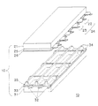
- FIG. 1 is an exploded perspective view of a plasma display panel 10 (hereinafter abbreviated as “panel”) of a plasma display device.
- panel a plasma display panel 10
- a plurality of display electrode pairs 24 formed of scanning electrodes 22 and sustaining electrodes 23 are formed on a glass front substrate 21.
- a dielectric layer 25 is formed so as to cover the display electrode pair 24, and a protective layer 26 is formed on the dielectric layer 25.
- a plurality of data electrodes 32 are formed on the rear substrate 31, a dielectric layer 33 is formed so as to cover the data electrodes 32, and a grid-like partition wall 34 is formed thereon.
- a phosphor layer 35 that emits red, green, and blue light is provided on the side surface of the partition wall 34 and on the dielectric layer 33.
- the front substrate 21 and the rear substrate 31 are arranged to face each other so that the display electrode pair 24 and the data electrode 32 intersect each other with a minute discharge space interposed therebetween, and the outer periphery thereof is sealed with a sealing material such as glass frit.
- a sealing material such as glass frit.
- a rare gas such as neon, argon, xenon, or a mixed gas thereof is sealed as a discharge gas.
- the discharge space is partitioned into a plurality of sections by partition walls 34, and a discharge cell is formed at each position where the display electrode pair 24 and the data electrode 32 intersect. These discharge cells discharge and emit light to display an image.
- the structure of the panel 10 is not limited to the above-described structure, and may be, for example, provided with a stripe-shaped partition wall.
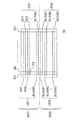
- FIG. 2 is an electrode array diagram of the panel 10 of the plasma display apparatus.
- the panel 10 includes n scan electrodes SC1, SC2,..., SCn (scan electrode 22 in FIG. 1) and n sustain electrodes SU1, SU2,. Sustain electrodes 23) are arranged, and m data electrodes D1, D2,..., Dm (data electrodes 32 in FIG. 1) that are long in the column direction are arranged.
- the 2160 display electrode pairs composed of the scan electrodes SC1 to SC2160 and the sustain electrodes SU1 to SU2160 are divided into a plurality of display electrode pair groups DG1, DG2,.
- a method for determining the number N of display electrode pair groups will be described later.
- the panel is divided into two vertically and divided into two display electrode pair groups DG1 and DG2.
- the display electrode pair located in the upper half of the panel is referred to as a display electrode pair group DG1
- the display electrode pair located in the lower half of the panel is referred to as a display electrode pair group DG2.
- 1080 scan electrodes SC1 to SC1080 are referred to as scan electrode group SG1, and 1080 sustain electrodes SU1 to SU1080 are referred to as sustain electrode group UG1.
- 1080 scan electrodes SC1081 to SC2160 are set as scan electrode group SG2, and 1080 sustain electrodes SU1081 to SU2160 are set as sustain electrode group UG2. That is, scan electrode group SG1 and sustain electrode group UG1 belong to display electrode pair group DG1, and scan electrode group SG2 and sustain electrode group UG2 belong to display electrode pair group DG2.
- the timing of the scanning pulse and the writing pulse is set so that the writing operation is continuously performed except for the initialization period.
- the maximum number of subfields can be set within one field period. The details will be described below with an example.
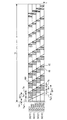
- FIG. 3 is a timing chart showing the subfield configuration of the plasma display device.
- the vertical axis represents scan electrodes SC1 to SC2160
- the horizontal axis represents time t.
- the write timing tW indicating the timing of performing the write operation is indicated by a thick solid line
- the sustain erase period timing tSE indicating the timing of the sustain period and the erase period described later is indicated by hatching.
- one field period Tf is 16.7 ms.
- an initializing period Tin for generating initializing discharges simultaneously in all the discharge cells is provided.
- the initialization period Tin is set to 500 ⁇ s.
- a period required to sequentially apply the scan pulse to all of the scan electrodes SC1 to SC2160 (that is, to perform the write operation once to all of the scan electrodes SC1 to SC2160).
- the total writing period Tw represented is estimated. At this time, it is desirable to apply the scan pulse as short as possible and continuously as possible so that the writing operation is continuously performed.
- the number N of display electrode pairs representing the number of display electrode pair groups DG1, DG2,..., DGN is determined based on the required number of sustain pulses.
- the number N of display electrode pairs representing the number of display electrode pair groups DG1, DG2,..., DGN is determined based on the required number of sustain pulses.
- a number of sustain pulses are applied to scan electrodes SC1 to SC2160.
- Sustain periods Ts1, Ts2,..., Ts10 representing periods required for applying sustain pulses are obtained by multiplying the number of sustain pulses described above in subfields SF1 to SF10 by the sustain pulse period.
- the writing period Tw1 represents the period required for the writing operation of each display electrode pair group DG1 to DGN in the entire writing period Tw, and is obtained by Expression 1.
- Tw1 Tw / N (1)
- the sustain periods Ts1 to Ts10 are provided after the write period Tw1 in the respective subfields SF1 to SF10.
- the number N of display electrode pair groups is obtained as a minimum integer that satisfies the following Expression 2 using the total writing period Tw and the maximum sustain period Ts1.
- Equation 2 The original equation of Equation 2 is Ts1 ⁇ Tw ⁇ (N ⁇ 1) / N (3) It is. Equation 3 shows that the maximum sustain period Ts1 should not exceed the remaining period obtained by subtracting the group unit write period Tw / N from the total write period Tw. In other words, it is necessary to determine the number N of display electrode pairs so that the period (Tw ⁇ (N ⁇ 1) / N) represented by the right side of Expression 3 is longer than the maximum sustain period Ts1.
- Equation 2 is expressed as a result of this derivation reason for Equation 3.
- the display electrode pairs are divided into two display electrode pair groups DG1 and DG2 as shown in FIG.
- N 2
- Tw 1512 ⁇ s
- Ts1 600 ⁇ s
- Tw ⁇ (N ⁇ 1) / N 756 ⁇ 600 (5)
- the condition of Equation 3 is satisfied.
- the drive configuration for driving the panel 10 and the number N of display electrode pair groups can be determined.
- the calculation is performed while ignoring the erase period.
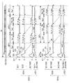
- FIG. 4 is a waveform diagram showing drive voltage waveforms applied to the respective electrodes of the panel 10 of the plasma display device.
- FIG. 4 shows, in order from the top, drive voltage waveforms of the data electrodes D1 to Dm, drive voltage waveforms of the scan electrode group SG1 and the sustain electrode group UG1 belonging to the display electrode pair group DG1, and scan electrodes belonging to the display electrode pair group DG2.
- the drive voltage waveforms of the group SG2 and the sustain electrode group UG2 are shown.
- an initialization period Tin for generating an initialization discharge in each discharge cell Cij is provided.
- subfields SF1 to SF10 are provided for each of the display electrode pair groups DG1 and DG2 in the same manner as in FIG.
- the erasing period Te is a period for generating an erasing discharge for the discharge cells discharged in the sustaining period after each of the sustaining periods Ts1 to Ts10. As described above with reference to FIG.
- the subfields SF1 to SF10 for the display electrode pair group DG2 are generally delayed by the writing period Tw1 as compared to the subfields SF1 to SF10 for the display electrode pair group DG1.
- the initialization period Tin will be described.
- the voltage 0 (V) is applied to the data electrodes D1 to Dm and the sustain electrodes SU1 to SU2160, respectively.
- Scan waveform SC1 to SC2160 is applied with a ramp waveform voltage that gradually increases from positive voltage Vi1 lower than the positive discharge start voltage to sustain electrodes SU1 to SU2160 to positive voltage Vi2 that exceeds the discharge start voltage, respectively. To do. While this ramp waveform voltage rises, a weak initializing discharge is generated between scan electrodes SC1 to SC2160, sustain electrodes SU1 to SU2160, and data electrodes D1 to Dm.
- Negative wall voltage is accumulated on scan electrodes SC1 to SC2160, and positive wall voltage is accumulated on data electrodes D1 to Dm and sustain electrodes SU1 to SU2160.
- the wall voltage on the electrode represents a voltage generated by wall charges accumulated on the dielectric layer covering the electrode, the protective layer, the phosphor layer, and the like. During this period, the voltage Vd may be applied to the data electrodes D1 to Dm.
- the voltage 0 (V) is applied to the data electrodes D1 to Dm
- the positive predetermined voltage Ve1 is applied to the sustain electrodes SU1 to SU2160
- the scan electrodes SC1 to SC2160 are positively connected to the sustain electrodes SU1 to SU2160, respectively.
- a ramp waveform voltage that gently falls from a positive voltage Vi3 lower than the discharge start voltage toward a negative voltage Vi4 that exceeds the negative discharge start voltage in the negative direction is applied.
- a weak initializing discharge is generated between scan electrodes SC1 to SC2160, sustain electrodes SU1 to SU2160, and data electrodes D1 to Dm.
- a positive predetermined voltage Ve2 higher than the predetermined voltage Ve1 is applied to the sustain electrode group UG1.
- a scan pulse having a negative voltage Va is applied to the scan electrode SC1
- the voltage difference at the intersection between the data electrode Dj and the scan electrode SC1 is the difference between the externally applied voltage (Vd ⁇ Va) and the difference between the wall voltage on the data electrode Dj and the wall voltage on the scan electrode SC1. It is added and exceeds the discharge start voltage.
- a discharge starts between data electrode Dj and scan electrode SC1, progresses to a discharge between sustain electrode SU1 and scan electrode SC1, and an address discharge is generated.
- a positive wall voltage is accumulated on scan electrode SC1
- a negative wall voltage is accumulated on sustain electrode SU1
- a negative wall voltage is also accumulated on data electrode Dj.
- the write discharge is generated in the discharge cell to be lit in the first row, and the write operation for accumulating the wall voltage on each electrode is performed.
- the voltage at the intersection of the data electrodes D1 to Dm to which the write pulse is not applied and the scan electrode SC1 does not exceed the discharge start voltage, so no write discharge occurs.
- a scan pulse is applied to the scan electrode SC2 in the second row, and an address pulse is applied to the data electrode Dj corresponding to the discharge cell to emit light. Then, an address discharge is generated in the discharge cells in the second row to which the scan pulse and the address pulse are simultaneously applied, and an address operation is performed.
- the above address operation is repeated until the discharge cell in the 1080th row, and an address discharge is selectively generated in the discharge cells to emit light to form wall charges.
- the voltage Vc is applied to the scan electrode group SG2 and the predetermined voltage Ve1 is applied to the sustain electrode group UG2.
- the writing period Tw1 is a rest period in which no discharge occurs with respect to the display electrode pair group DG2.
- the voltage applied to each electrode belonging to the display electrode pair group DG2 is not limited to the voltage described above, and another voltage within a range where no discharge is generated may be applied.
- a predetermined positive voltage Ve2 is applied to sustain electrode group UG2.
- a scan pulse is applied to scan electrode SC1081, and a write pulse is applied to data electrode Dj corresponding to the discharge cell to emit light.
- an address discharge is generated between data electrode Dj and scan electrode SC1081, and between sustain electrode SU1081 and scan electrode SC1081.
- a scan pulse is applied to scan electrode SC1082, and a write pulse is applied to data electrode Dj corresponding to the discharge cell to emit light.
- the write discharge is generated in the discharge cells in the row 1082 to which the scan pulse and the write pulse are simultaneously applied.
- the above address operation is repeated until the discharge cell in the 2160th row, and an address discharge is selectively generated in the discharge cells to emit light to form wall charges.
- the writing period Tw1 of the subfield SF1 for the display electrode pair group DG2 corresponds to the sustain period Ts1 of the subfield SF1 for the display electrode pair group DG1. That is, “60” sustain pulses are applied to scan electrode group SG1 and “60” sustain pulses are applied alternately to sustain electrode group UG1 one by one to perform address discharge, thereby causing the discharge cells to emit light.
- positive sustain pulse voltage Vs is applied to scan electrode group SG1, and voltage 0 (V) is applied to sustain electrode group UG1.
- sustain pulse voltage Vs is added to the difference between the wall voltage on scan electrode SCi and the wall voltage on sustain electrode SUi, and the voltage between scan electrode SCi and sustain electrode SUi is increased. The difference exceeds the discharge start voltage. Therefore, a sustain discharge occurs between scan electrode SCi and sustain electrode SUi, and phosphor layer 35 emits light due to the ultraviolet rays generated at this time.
- a negative wall voltage is accumulated on scan electrode SCi, and a positive wall voltage is accumulated on sustain electrode SUi.
- no sustain discharge occurs, and the wall voltage at the end of the initialization period Tin is maintained.
- V voltage 0 (V) is applied to scan electrode group SG1, and positive sustain pulse voltage Vs is applied to sustain electrode group UG1.
- the voltage difference between the sustain electrode SUi and the scan electrode SCi exceeds the discharge start voltage, so that the sustain discharge occurs again between the sustain electrode SUi and the scan electrode SCi, Negative wall voltage is accumulated on sustain electrode SUi, and positive wall voltage is accumulated on scan electrode SCi.
- the sustain discharge is alternately applied to the scan electrode group SG1 and the sustain electrode group UG1, and a potential difference is applied between the electrodes of the display electrode pair, whereby the sustain discharge is generated in the discharge cell in which the address discharge is generated in the address period Tw1. Occurs continuously, and the discharge cell emits light.
- An erasing period Te is provided after the maintenance period Ts1.
- a so-called narrow pulse voltage difference is applied between the scan electrodes SC1 to SCn and the sustain electrodes SU1 to SUn, leaving the positive wall voltage on the data electrode Dj and the scan electrodes SCi and SCn.
- the wall voltage on the sustain electrode SUi is erased.
- a predetermined positive voltage Ve2 is applied to sustain electrode group UG1.
- scan pulses are sequentially applied in the same manner as in the write period Tw1 of the subfield SF1, and a write pulse is applied to the data electrode Dj to perform a write operation in the discharge cells in the first to 1080th rows. I do.
- the write period Tw1 of the subfield SF2 for the display electrode pair group DG1 corresponds to the sustain period Ts1 of the subfield SF1 for the display electrode pair group DG2.
- “60” sustain pulses are alternately applied to the scan electrode group SG2 and the sustain electrode group UG2 one by one to perform address discharge, thereby causing the discharge cells to emit light.
- the erasing period Te after the sustain period Ts1 a narrow pulse-shaped voltage difference is given between the scan electrode group SG2 and the sustain electrode group UG2, leaving a positive wall voltage on the data electrode Dj.
- the wall voltages on scan electrode SCi and sustain electrode SUi are erased.
- the writing period Tw1 of the subfield SF2 for the display electrode pair group DG2 the writing period Tw1 of the subfield SF3 for the display electrode pair group DG1,..., And the writing period Tw1 of the subfield SF10 for the display electrode pair group DG2.
- the sustaining period Ts10 and the erasing period Te of the subfield SF10 for the display electrode pair group DG2 are finally ended, followed by one field period Tf.
- one field period Tf includes an initialization period Tin, a portion corresponding to subfields SF1 to SF10 (Tw ⁇ 10) of the entire writing period Tw, a sustain period Ts10 of the subfield SF10, It may be equal to or greater than the sum total with the erasing period Te of the field SF10.
- the sustain periods Ts1 to Ts9 and the erasure period Te in the subfields SF1 to SF9 are substantially ignored since they are temporally parallel to the subfields SF1 to SF10 equivalent to the entire write period Tw (Tw ⁇ 10). Can do.
- ten subfields SF1 to SF10 can be set within one field period Tf.
- the number of subfields SF1 to SF10 is the maximum number that can be set within one field period Tf as described above.
- one field period Tf is finally ended in the sustain period Ts10 and the erasing period Te for the display electrode pair group DG2 (see Expression 6). Therefore, the sustain period Ts10 of Expression 6 can be shortened by arranging the sustain period Ts10 having the smallest luminance weight in the last subfield SF10.
- the erasing operation is performed by applying a narrow pulse voltage difference between the scan electrodes SC1 to SCn and the sustaining electrodes SU1 to SUn, and the erasing period Te is ignored.
- the subfield configuration and display electrode pair group number N were determined. Further, it has been described that the write operation is performed even if one of the display electrode pair groups DG1 and DG2 is in the erasing period Te. However, in order to perform the erasing operation, a certain erasing period Te is required, and as described above, the writing operation is performed when one of the display electrode pair groups DG1 and DG2 is in the erasing period Te. Desirably not.
- FIG. 5 is a block diagram of the plasma display device 40.
- the plasma display device 40 includes a plasma display panel drive circuit 46 and a panel 10.
- the plasma display panel drive circuit 46 is necessary for the image signal processing circuit 41, the data electrode drive circuit 42, the scan electrode drive circuit 43a, the scan electrode drive circuit 43b, the sustain electrode drive circuit 44, the timing generation circuit 45, and each circuit block.
- a power supply circuit (not shown) for supplying a proper power supply is provided.
- the timing generation circuit 45 generates various timing signals S45 for controlling the operation of each circuit based on the horizontal synchronization signal and the vertical synchronization signal of the image signal, and supplies them to the respective circuits.
- the image signal processing circuit 41 converts the image signal into image data indicating light emission / non-light emission for each subfield based on the timing signal S45.
- the data electrode drive circuit 42 includes m switches for applying a voltage Vd or a voltage 0 (V) to each of the m data electrodes D1 to Dm. Based on the timing signal S45, the data electrode drive circuit 42 converts the image data output from the image signal processing circuit 41 into a write pulse corresponding to each data electrode D1 to Dm, and applies it to each data electrode D1 to Dm. To do.
- the scan electrode driving circuit 43a drives the scan electrode group SG1 based on the timing signal S45
- the scan electrode drive circuit 43b drives the scan electrode group SG2 based on the timing signal S45
- Sustain electrode drive circuit 44 drives sustain electrode groups UG1 and UG2 based on timing signal S45.
- the timing signal S45 from the timing generation circuit 45 is shown. The wiring is omitted for simplicity of illustration.
- FIG. 6 is a circuit diagram of the scan electrode drive circuits 43a and 43b in the drive circuit 46 of the plasma display panel.
- Scan electrode drive circuit 43a includes sustain pulse generation circuit 50a, initialization waveform generation circuit 60a, and scan pulse generation circuit 70a.
- Sustain pulse generation circuit 50a has power recovery unit 51a and voltage clamp unit 55a, and applies a sustain pulse to scan electrode group SG1.
- the power recovery unit 51a includes a power recovery capacitor C51a, switching elements Q51a and Q52a, backflow prevention diodes D51a and D52a, and a resonance inductor L51a.
- One end of capacitor C51a is grounded, and the other end is connected to one end of switching element Q51a and one end of switching element Q52a.
- the other end of switching element Q51a is connected to the anode of diode D51a, and the other end of switching element Q52a is connected to the cathode of diode D52a.
- the cathode of the diode D51a and the anode of the diode D52a are commonly connected to one end of the inductor L51a, and the other end of the inductor L51a is connected to a connection point between the switching element Q55a and the switching element Q56a in the voltage clamp portion 55a.
- the power recovery unit 51a causes LC resonance between the 1080 interelectrode capacitances between the scan electrode group SG1 and the sustain electrode group UG1 constituting the display electrode pair group DG1, and the rise and fall of the sustain pulse. I do.
- the power recovery unit 51a uses the charge (or power) stored in the power recovery capacitor C51a to generate a switching element Q51a, a diode D51a, an inductor L51a, an initialization waveform generation circuit 60a, and a scan pulse.
- the circuit 70a and the scan electrode group SG1 1080 inter-electrode capacitors are supplied.
- the power recovery unit 51a transfers the charge (or power) stored in the 1080 interelectrode capacitances from the scan electrode group SG1 to the scan pulse generation circuit 70a and the initialization waveform generation circuit 60a.
- the power is recovered in the capacitor C51a for power recovery via the inductor L51a, the diode D52a, and the switching element Q52a.
- the power recovery unit 51a drives the scan electrode group SG1 by LC resonance without supplying power from the power source, the power consumption is ideally “0”.
- the power recovery capacitor C51a has a capacity sufficiently larger than the 1080 interelectrode capacity, and is approximately half of the power supply voltage Vs supplied for the sustain discharge so as to serve as a power source for the power recovery section 51a. It is charged to Vs / 2.
- the voltage clamp part 55a has switching elements Q55a and Q56a.
- Scan electrode group SG1 is connected to the power supply via switching element Q55a, and is clamped at power supply voltage Vs when switching element Q55a is turned on.
- Scan electrode group SG1 is grounded via switching element Q56a, and is clamped at voltage 0 (V) when switching element Q56a is turned on.
- the power supply voltage Vs corresponds to the pulse peak voltage of the sustain pulse
- the voltage 0 (V) corresponds to the pulse reference voltage of the sustain pulse.
- the voltage clamp unit 55a applies the sustain pulse to the scan electrode group SG1 by alternately clamping the scan electrode group SG1 during the sustain period to the pulse peak voltage and the pulse reference voltage of the sustain pulse.
- the voltage clamp portion 55a has a small impedance when a voltage is applied, and a large discharge current due to a strong sustain discharge can flow stably.
- sustain pulse generating circuit 50a generates a sustain pulse by controlling switching elements Q51a, Q52a, Q55a, and Q56a based on timing signal S45, and via initialization waveform generating circuit 60a and scan pulse generating circuit 70a.
- a sustain pulse is applied to scan electrode group SG1.
- These switching elements Q51a, Q52a, Q55a, and Q56a are MOSFETs (Metal Oxide Semiconductor Field Effect Transistors) and IGBTs (Insulated Gate Bipolar Transistors). Can be configured.
- FIG. 6 shows a circuit configuration using, for example, a MOSFET as a switching element. In order to make the drawing easier to see, the MOSFET body diode is omitted.
- the initialization waveform generation circuit 60a includes a Miller integration circuit 61a, a Miller integration circuit 62a, a switching element Q63a, and a switching element Q64a.
- Miller integrating circuit 61a applies a gradually increasing ramp waveform voltage to scan electrode group SG1 in initialization period Tin.
- Miller integrating circuit 62a applies a gradually decreasing ramp waveform voltage to scan electrode group SG1 in initialization period Tin.
- Switching elements Q63a and Q64a are separation switches, and are provided to prevent a current from flowing back through the parasitic diodes of the switching elements constituting sustain pulse generating circuit 50a and initialization waveform generating circuit 60a.
- the initialization waveform generating circuit 60a applies the initialization pulse to the scan electrode group SG1 by controlling the Miller integrating circuits 61a and 62a and the switching elements Q63a and Q64a based on the timing signal S45.
- Scan electrode drive circuit 43b has the same configuration as scan electrode drive circuit 43a, and applies a sustain pulse, an initialization waveform, and a scan pulse to scan electrode group SG2.
- the sustain electrode driving circuit is provided for each of the plurality of display electrode pair groups, and for each of the plurality of display electrode pair groups, a sustain pulse generating circuit for applying a sustain pulse to the sustain electrodes belonging to the display electrode pair group
- a predetermined voltage applying circuit for applying a predetermined voltage to the sustain electrodes belonging to the display electrode pair group
- a voltage selecting circuit for selecting one voltage from the plurality of voltages and supplying the selected voltage to each of the plurality of sustain pulse generating circuits
- the predetermined voltage application circuit is also called a constant voltage generation circuit.
- the predetermined voltage is also called a constant voltage.
- the constant voltage generation circuit applies a constant voltage to the sustain electrodes belonging to the display electrode pair group.
- FIG. 7 is a circuit diagram of the sustain electrode drive circuit 44 in the drive circuit 46 of the plasma display panel.
- the 2160 display electrode pairs including scan electrodes SC1 to SC2160 and sustain electrodes SU1 to SU2160 constituting plasma display panel 10 are divided into display electrode pair groups DG1 and DG2.
- Display electrode pair group DG1 includes scan electrode group SG1 and sustain electrode group UG1
- display electrode pair group DG2 includes scan electrode group SG2 and sustain electrode group UG2. That is, the plurality of sustain electrodes SU1 to SU2160 constituting the plasma display panel 10 are divided into a sustain electrode group UG1 and a sustain electrode group UG2.
- Sustain electrode drive circuit 44 applies a sustain pulse to sustain electrode group UG1 and sustain electrode group UG2 in sustain periods Ts1 to Ts10.
- Sustain electrode drive circuit 44 includes two sustain pulse generation circuits 80a and 80b, two predetermined voltage application circuits 90a and 90b, one voltage selection circuit 100, an electrode path RG1, and an electrode path RG2.
- Sustain electrode drive circuit 44 is connected to sustain electrode group UG1 via electrode path RG1, and is connected to sustain electrode group UG2 via electrode path RG2.
- the electrode path RG1 represents an output path to the sustain electrode group UG1 or an input path from the sustain electrode group UG1 in the sustain electrode drive circuit 44.
- the electrode path RG2 represents an output path to the sustain electrode group UG2 or an input path from the sustain electrode group UG2 in the sustain electrode drive circuit 44.
- the voltage selection circuit 100 includes a power supply path RS, a power supply path R1, a switching element Q101, and a switching element Q102.
- the predetermined voltage source ES generates a predetermined voltage Vs
- the power supply path RS receives the predetermined voltage Vs.
- the predetermined voltage source E1 generates a predetermined voltage Ve1
- the power supply path R1 receives the predetermined voltage Ve1.
- Switching element Q101 is connected between power supply path RS and sustain pulse generating circuits 80a and 80b
- switching element Q102 is connected between power supply path R1 and sustain pulse generating circuits 80a and 80b.
- the power supply path may be a power supply terminal.
- the voltage selection circuit 100 selects any one of a plurality of predetermined voltages, and generates a selection voltage V3 representing the selected predetermined voltage. In one example, the voltage selection circuit 100 selects one of the predetermined voltages Vs and Ve1 and generates a selection voltage V3. When the switching element Q101 is turned on, the voltage selection circuit 100 selects the predetermined voltage Vs and sets the selection voltage V3 to the predetermined voltage Vs. On the other hand, when the switching element Q102 is turned on, the voltage selection circuit 100 selects the predetermined voltage Ve1 and sets the selection voltage V3 to the predetermined voltage Ve1. As described above, the voltage selection circuit 100 generates the selection voltage V3 by controlling the switching elements Q101 and Q102 based on the timing signal S45.
- the switching element Q102 is provided to allow a current to flow from the sustain pulse generation circuits 80a and 80b to the predetermined voltage source E1 via the power supply path R1. However, when a current is allowed to flow only from the predetermined voltage source E1 to the sustain pulse generation circuits 80a and 80b via the power supply path R1, it may be replaced with a diode.
- Sustain pulse generation circuit 80a has power recovery unit 81a and voltage clamp unit 85a.
- the power recovery unit 81a includes a power recovery capacitor C81a, switching elements Q81a and Q82a, backflow prevention diodes D81a and D82a, and a resonance inductor L81a.
- the voltage clamp unit 85a includes a high voltage side path R3H, a low voltage side path R3L, switching elements Q85a and Q86a, and diodes D85a and D86a.
- the switching element Q85a is an example of a high voltage side switching element
- the switching element Q86a is an example of a low voltage side switching element.
- One end of the capacitor C81a is grounded, and the other end is connected to one end of the switching element Q81a and one end of the switching element Q82a.
- the other end of switching element Q81a is connected to the anode of diode D81a, and the other end of switching element Q82a is connected to the cathode of diode D82a.
- the cathode of diode D81a and the anode of diode D82a are connected to one end of inductor L81a.
- the other end of the inductor L81a is commonly connected to a connection point between the switching element Q85a and the switching element Q86a in the voltage clamp portion 85a.
- sustain pulse generation circuit 80b includes power recovery unit 81b and voltage clamp unit 85b.
- the power recovery unit 81b includes a power recovery capacitor C81b, switching elements Q81b and Q82b, backflow prevention diodes D81b and D82b, and a resonance inductor L81b.
- the voltage clamp unit 85b includes a high voltage side path R3H, a low voltage side path R3L, switching elements Q85b and Q86b, and diodes D85b and D86b.
- the switching element Q85b is an example of a high voltage side switching element
- the switching element Q86b is an example of a low voltage side switching element.
- FIG. 7 shows a circuit configuration using an IGBT.
- the switching elements Q85a, Q86a, Q85b, and Q86b constituting the voltage clamp portions 85a and 85b the forward direction of the controlled current (that is, the forward current direction flowing from the collector to the emitter) is It is necessary to provide a reverse current characteristic by providing a current path in the reverse direction.
- the diodes D85a, D86a, D85b, and D86b are connected in parallel to the switching elements Q85a, Q86a, Q85b, and Q86b so that the current forward directions are opposite to each other.
- a diode may be connected in parallel to each of the switching elements Q81a, Q82a, Q81b, Q82b in order to protect the IGBT.
- the parallel circuit of the switching element Q85a and the diode D85a is connected between the high voltage side path R3H and the electrode path RG1, and the parallel circuit of the switching element Q86a and the diode D86a is connected to the low voltage side path R3L. It is connected between the electrode path RG1.
- the parallel circuit of the switching element Q85b and the diode D85b is connected between the high voltage side path R3H and the electrode path RG2, and the parallel circuit of the switching element Q86b and the diode D86b is connected to the low voltage side. Connected between the path R3L and the electrode path RG2.
- the high voltage side path R3H is connected to the switching elements Q101 and Q102 of the voltage selection circuit 100, and the low voltage side path R3L is grounded.
- sustain pulse generating circuit 80a The operation of sustain pulse generating circuit 80a is the same as the operation of sustain pulse generating circuit 50a. That is, when the sustain pulse rises, the power recovery unit 81a transfers the charge (or power) stored in the power recovery capacitor C81a via the switching element Q81a, the diode D81a, the inductor L81a, and the electrode path RG1. The voltage is supplied to the interelectrode capacitance of sustain electrodes SU1 to SU1080 belonging to sustain electrode group UG1.
- the power recovery unit 81a uses the charge (or power) stored in the interelectrode capacitance of the sustain electrodes SU1 to SU1080 as the electrode path RG1, the inductor L81a, the diode D82a, and the switching element Q82a. Then, the power is recovered in the capacitor C81a for power recovery.
- the high voltage side path R3H receives the selection voltage V3, and the low voltage side path R3L receives the predetermined voltage 0 (V).
- the sustain electrode group UG1 is clamped to the selection voltage V3 in the high voltage side path R3H when the switching element Q85a is turned on.
- the sustain electrode group UG1 is clamped to the predetermined voltage Vs when the selection voltage V3 is the predetermined voltage Vs, and is clamped to the predetermined voltage Ve1 when the selection voltage V3 is the predetermined voltage Ve1.
- Sustain electrode group UG1 is clamped at a predetermined voltage of 0 (V) when switching element Q86a is turned on.
- the predetermined voltage Vs corresponds to the pulse peak voltage of the sustain pulse
- the predetermined voltage 0 (V) corresponds to the pulse reference voltage of the sustain pulse.
- the voltage clamp unit 85a applies the sustain pulse to the sustain electrode group UG1 by alternately clamping the sustain electrode group UG1 during the sustain period to the pulse peak voltage and the pulse reference voltage of the sustain pulse.
- the voltage clamp unit 85a has a small impedance when a voltage is applied, and a large discharge current due to a strong sustain discharge can flow stably.
- sustain pulse generating circuit 80a generates sustain pulses by controlling switching elements Q81a, Q82a, Q85a, and Q86a based on timing signal S45, and maintains sustain pulses in sustain electrode group UG1 via electrode path RG1. Apply a pulse. Further, sustain pulse generation circuit 80a receives predetermined voltage Ve1 from voltage selection circuit 100 in high-voltage side path R3H, and applies predetermined voltage Ve1 to sustain electrode group UG1 through electrode path RG1.
- sustain pulse generating circuit 80b The operation of sustain pulse generating circuit 80b is the same as the operation of sustain pulse generating circuit 80a. That is, sustain pulse generation circuit 80b generates a sustain pulse by repeatedly generating a pulse peak voltage and a pulse reference voltage, and applies the sustain pulse to sustain electrode group UG2 via electrode path RG2. Further, sustain pulse generating circuit 80b receives predetermined voltage Ve1 from voltage selection circuit 100 in high voltage side path R3H and applies it to sustain electrode group UG2 through electrode path RG2.
- the predetermined voltage application circuit 90a includes a power supply path R2, a switching element Q91a, and a switching element Q92a.
- the predetermined voltage source E2 generates a predetermined voltage Ve2
- the power supply path R2 receives the predetermined voltage Ve2.
- Switching element Q91a and switching element Q92a are bidirectionally connected in series so that the forward direction of the controlled current (that is, the forward current direction flowing from the drain to the source or from the collector to the emitter) is opposite to each other.
- the switch is formed.
- the series connection circuit of switching element Q91a and switching element Q92a is connected between power supply path R2 and electrode path RG1.
- the predetermined voltage application circuit 90a is turned on when the switching element Q91a and the switching element Q92a are simultaneously turned on, and is turned off when being simultaneously turned off.
- the predetermined voltage application circuit 90a is turned on, the predetermined voltage Ve2 is applied to the sustain electrode group UG1 via the electrode path RG1.
- the predetermined voltage application circuit 90a is turned off, the power supply path R2 and the sustain electrode group UG1 are electrically disconnected. In this manner, the predetermined voltage application circuit 90a applies the predetermined voltage Ve2 to the sustain electrode group UG1 via the electrode path RG1 by being controlled based on the timing signal S45.
- the predetermined voltage application circuit 90b includes a power supply path R2, a switching element Q91b, and a switching element Q92b.
- Switching element Q91b and switching element Q92b form a bidirectional switch connected in series so that the forward directions of the currents to be controlled are opposite to each other.
- the series connection circuit of switching element Q91b and switching element Q92b is connected between power supply path R2 and electrode path RG2.
- the predetermined voltage application circuit 90b is turned on when the switching element Q91b and the switching element Q92b are turned on simultaneously, and turned off when the switching element Q91b is turned off at the same time.
- the predetermined voltage application circuit 90b is turned on, the predetermined voltage Ve2 is applied to the sustain electrode group UG2 via the electrode path RG2.
- the predetermined voltage application circuit 90b When the predetermined voltage application circuit 90b is turned off, the power supply path R2 and the sustain electrode group UG2 are electrically disconnected. Thus, the predetermined voltage application circuit 90b is controlled based on the timing signal S45, and thereby applies the predetermined voltage Ve2 to the sustain electrode group UG2 via the electrode path RG2.
- the switching elements constituting the voltage selection circuit 100 and the predetermined voltage application circuits 90a and 90b can also be configured using transistor elements such as MOSFETs and IGBTs.
- FIG. 7 shows a circuit configuration using a MOSFET.
- an IGBT is used as a switching element, a reverse current characteristic of the IGBT is ensured by providing a current path in a direction opposite to the forward direction of the controlled current (that is, the forward current direction flowing from the collector to the emitter).
- a diode in parallel with the IGBT FIG. 7 clearly shows the body diode of each MOSFET.
- Switching elements Q91a and Q91b can be replaced with diodes when current flows from predetermined voltage source E2 only to sustain electrode groups UG1 and UG2, respectively.
- FIG. 8 is a waveform diagram showing the operation of the sustain electrode drive circuit 44 in the drive circuit 46 of the plasma display panel.
- the upper half of FIG. 8 shows drive voltage waveforms applied to the sustain electrode group UG1 and the sustain electrode group UG2.
- the lower half of FIG. 8 shows a state in which switching elements Q85a, Q86a, Q85b, and Q86b, predetermined voltage application circuits 90a and 90b, and switching elements Q101 and Q102 are turned on / off based on timing signal S45. Yes.
- the ON state is indicated as ON and the OFF state is indicated as OFF.
- the switching element Q86a In order to apply the predetermined voltage 0 (V) to the sustain electrode groups UG1 and UG2 in the initialization period Tin, the switching element Q86a is turned on and the sustain electrode group UG1 is grounded. At the same time, the switching element Q86b is turned on to ground the sustain electrode group UG2.
- the switching elements Q86a and Q86b are turned off. Then, switching element Q102 is turned on to supply predetermined voltage Ve1 to sustain pulse generating circuits 80a and 80b. Further, the switching element Q85a is turned on, and the sustain electrode group UG1 is clamped to the predetermined voltage Ve1. At the same time, the switching element Q85b is turned on, and the sustain electrode group UG2 is clamped to the predetermined voltage Ve1.
- the switching element Q85a is turned off and the predetermined voltage application circuit 90a is turned on to apply the predetermined voltage Ve2 to the sustain electrode group UG1.
- the switching element Q85b is turned off and the predetermined voltage application circuit 90b is turned on to apply the predetermined voltage Ve2 to the sustain electrode group UG2.
- the switching element Q101 is turned on to supply the predetermined voltage Vs to the sustain pulse generating circuits 80a and 80b. Then, the predetermined voltage application circuit 90a is turned off, and the sustain pulse generated by the sustain pulse generation circuit 80a is applied to the sustain electrode group UG1.
- switching elements Q81a, Q85a, and Q86a are turned off, then switching element Q82a is turned on, and the voltage of sustain electrode group UG1 is set to a predetermined voltage 0 (V) by LC resonance. ) Reduce to near. Thereafter, switching element Q86a is turned on, and sustain electrode group UG1 is clamped to a predetermined voltage of 0 (V). Next, after switching elements Q82a and Q86a are turned off, switching element Q81a is turned on, and the voltage of sustain electrode group UG1 is raised to the vicinity of predetermined voltage Vs by LC resonance. Thereafter, the switching element Q85a is turned on, and the sustain electrode group UG1 is clamped to the predetermined voltage Vs. By repeating the above operation, sustain pulse generating circuit 80a can generate a sustain pulse.
- the predetermined voltage Ve2 is continuously applied to the sustain electrode group UG2.
- the switching elements Q81a, Q82a, Q85a, and Q86a are turned off, the predetermined voltage application circuit 90a is turned on, and the predetermined voltage Ve2 is applied to the sustain electrode group UG1. To do. Thereafter, in the writing period Tw1 of the subfield SF2 in the sustain electrode group UG1, the on / off state of each switching element is continued.
- the predetermined voltage application circuit 90b is turned off and generated in the sustain pulse generation circuit 80b.
- the sustained sustain pulse is applied to sustain electrode group UG2.
- the sustaining electrode belonging to the sustaining electrode group in the writing period Tw1 is turned off the switching element of the corresponding sustaining pulse generating circuit, and the predetermined voltage applying circuit is turned on to apply the predetermined voltage Ve2. Then, to the sustain electrodes belonging to the sustain electrode group that is in the sustain period, the corresponding predetermined voltage application circuit is turned off, and the sustain pulse is applied by controlling the switching element of the corresponding sustain pulse generation circuit.
- the drive voltage waveform shown in FIG. 8 can be applied to the sustain electrodes belonging to the sustain electrode groups UG1 and UG2.
- sustain electrode driving circuit 44 in the first embodiment selects one predetermined voltage from predetermined voltage Vs and predetermined voltage Ve1, and supplies the voltage to each of two sustain pulse generating circuits 80a and 80b. 100.
- the number of switching elements can be reduced compared with the case where the same number of sustain electrode drive circuits as the number of display electrode pair groups is provided, and a simple sustain electrode drive circuit is realized.
- two switching elements are provided in order to supply the predetermined voltage Ve1 to each sustain electrode drive circuit, for a total of four switching elements. Is required.
- the four switching elements described above can be eliminated, so that the number of switching elements can be reduced by two. it can.
- the present invention is not limited to this, and can be applied even when the display electrode pairs are divided into three or more display electrode pair groups. Moreover, the effect of reducing switching elements increases as the number of display electrode pair groups increases. An example in which the display electrode pairs are divided into four display electrode pair groups will be described below.
- FIG. 9 is an electrode array diagram of the panel 10 of the plasma display device 40.
- the panel is divided into four display electrode pair groups by dividing the panel into four in the vertical direction.
- a display electrode pair group DG11, a display electrode pair group DG12, a display electrode pair group DG21, and a display electrode pair group DG22 are sequentially arranged from the display electrode pair located at the top of the panel.
- 540 scan electrodes SC1 to SC540 are set as scan electrode group SG11
- 540 sustain electrodes SU1 to SU540 are set as sustain electrode group UG11.
- 540 scan electrodes SC541 to SC1080 are set as scan electrode group SG12, and 540 sustain electrodes SU541 to SU1080 are set as sustain electrode group UG12. Further, 540 scan electrodes SC1081 to SC1620 are set as scan electrode group SG21, and 540 sustain electrodes SU1081 to SU1620 are set as sustain electrode group UG21. Further, 540 scan electrodes SC1621 to SC2160 are set as scan electrode group SG22, and 540 sustain electrodes SU1621 to SU2160 are set as sustain electrode group UG22.
- scan electrode group SG11 and sustain electrode group UG11 belong to display electrode pair group DG11
- scan electrode group SG12 and sustain electrode group UG12 belong to display electrode pair group DG12.
- scan electrode group SG21 and sustain electrode group UG21 belong to display electrode pair group DG21
- scan electrode group SG22 and sustain electrode group UG22 belong to display electrode pair group DG22.
- FIG. 10 is a timing chart showing a subfield configuration of the plasma display device 40.
- the vertical axis represents scan electrodes SC1 to SC2160, and the horizontal axis represents time t.
- the write timing tW indicating the timing of performing the write operation is indicated by a thick solid line.
- the sustain period timing tS representing the sustain period timing is indicated by thin hatching.
- the erase period timing tE representing the erase period timing is indicated by thick hatching.
- the erasing period Te is provided immediately before the writing period of the next subfield. Then, in the field period Tf excluding the initialization period Tin and the respective erasing periods Te, the display electrode pair groups are driven so as to continuously perform the writing operation. In addition, an erasing period in which no discharge is generated is provided between the sustaining period and the writing period so that the sustaining period ends immediately before the erasing period Te. As described above, by providing the erase period immediately after the sustain period, the erase discharge can be performed using the priming generated by the sustain discharge, and a stable erase operation can be performed.
- the 1 field period Tf is 16.7 ms
- the initialization period Tin is 500 ⁇ s
- the period required for the write operation per scan electrode is 0.7 ⁇ s. Therefore, the total writing period Tw representing the period necessary for performing the writing operation once in all the scan electrodes SC1 to SC2160 is 1512 ⁇ s, and 10 subfields can be secured at the maximum.
- “110”, “81”, “55”, “33”, “20”, “11”, “6”, “4”, “2”, “ 1 ”number of sustain pulses were applied. The number of these sustain pulses is an average of slightly less than twice that of the first embodiment.
- the number N of display electrode pair groups is 4 because it is the smallest integer that satisfies Expression 7. In this way, by dividing the display electrode pairs into four display electrode pair groups, the number of sustain pulses can be increased on average by a little less than twice as compared with the case of two display electrode pair groups. Brightness can be increased.
- FIG. 11 is a circuit diagram of the sustain electrode driving circuit 144 in the driving circuit 46 of the plasma display panel.
- Sustain electrode drive circuit 144 includes four sustain pulse generation circuits 180a, 180b, 180c, and 180d, four predetermined voltage application circuits 190a, 190b, 190c, and 190d, one voltage selection circuit 100, and four electrode paths RG11. , RG12, RG21, and RG22.
- Sustain electrode drive circuit 144 is connected to sustain electrode group UG11 via electrode path RG11, connected to sustain electrode group UG12 via electrode path RG12, and connected to sustain electrode group UG21 via electrode path RG21. It is connected to sustain electrode group UG22 via path RG22.
- Electrode path RG11 represents an output path to sustain electrode group UG11 or an input path from sustain electrode group UG11 in sustain electrode drive circuit 144.
- the electrode path RG12 represents an output path to the sustain electrode group UG12 or an input path from the sustain electrode group UG12 in the sustain electrode drive circuit 144.
- the electrode path RG21 represents an output path to the sustain electrode group UG21 or an input path from the sustain electrode group UG21 in the sustain electrode drive circuit 144.
- the electrode path RG22 represents an output path to the sustain electrode group UG22 or an input path from the sustain electrode group UG22 in the sustain electrode drive circuit 144.
- the voltage selection circuit 100 has the same configuration as the voltage selection circuit 100 in the first embodiment and operates in the same manner. That is, the voltage selection circuit 100 selects one of the predetermined voltages Vs and Ve1, and supplies the selected predetermined voltage to the high-voltage side path R3H.
- Each sustain pulse generation circuit 180a, 180b, 180c, 180d has the same configuration as sustain pulse generation circuit 80a in the first embodiment and operates in the same manner. That is, sustain pulse generating circuits 180a, 180b, 180c, and 180d generate sustain pulses by repeatedly generating a pulse peak voltage and a pulse reference voltage, and apply them to sustain electrode groups UG11, UG12, UG21, and UG22, respectively. Further, sustain pulse generation circuits 180a, 180b, 180c, and 180d receive predetermined voltage Ve1 from voltage selection circuit 100 in high voltage side path R3H and apply it to sustain electrode groups UG11, UG12, UG21, and UG22, respectively.
- Each predetermined voltage application circuit 190a, 190b, 190c, 190d has the same configuration as the predetermined voltage application circuit 90a in the first embodiment and operates in the same manner. That is, the predetermined voltage application circuits 190a, 190b, 190c, and 190d are turned on to apply the predetermined voltage Ve2 to the sustain electrode groups UG11, UG12, UG21, and UG22, respectively.
- the predetermined voltage application circuits 190a, 190b, 190c, and 190d are electrically turned off from the power supply path R2 and the sustain electrode groups UG11, UG12, UG21, and UG22, respectively.
- predetermined voltage application circuits 190a, 190b, 190c, and 190d are configured such that when a current flows only from the predetermined voltage source E2 toward the sustain electrode groups UG11, UG12, UG21, and UG22, one of the switching elements is a diode. Can be replaced.
- sustain electrode driving circuit 144 in the second embodiment selects one predetermined voltage from predetermined voltage Vs and predetermined voltage Ve1, and supplies it to each of four sustain pulse generating circuits 180a, 180b, 180c, and 180d.
- the voltage selection circuit 100 is provided. With this circuit configuration, the number of switching elements can be reduced compared with the case where the same number of sustain electrode drive circuits as the number of display electrode pair groups is provided, and a simple sustain electrode drive circuit is realized. In fact, assuming that the same number of sustain electrode driving circuits as the number of display electrode pair groups are provided, two switching elements are provided to supply a predetermined voltage Ve1 to each sustain electrode driving circuit, for a total of eight switching elements. Necessary. However, according to the second embodiment, by adding the two switching elements Q101 and Q102 constituting the voltage selection circuit 100, the above-described eight switching elements can be eliminated, so that the number of switching elements can be reduced by six. it can.
- the voltage selection circuit 100 is configured to supply the predetermined voltage Vs or the predetermined voltage Ve1 to the high voltage side path R3H of the sustain pulse generating circuit.
- the present invention is not limited to this configuration.
- a sustain electrode driving circuit including a voltage selection circuit that supplies a predetermined voltage 0 (V) or a predetermined voltage Ve1 to the low-voltage side path R3L of the sustain pulse generation circuit will be described.
- the panel is divided into two in the vertical direction and divided into two display electrode pair groups DG1 and DG2.
- Scan electrodes SC1 to SC1080 (ie, scan electrode group SG1) and sustain electrodes SU1 to SU1080 (ie, sustain electrode group UG1) belong to display electrode pair group DG1
- scan electrodes SC1081 to SC2160 ie, scan electrode group SG2
- sustain electrodes SU1081 to SU2160 that is, sustain electrode group UG2
- FIG. 12 is a circuit diagram of the sustain electrode drive circuit 244 in the drive circuit 46 of the plasma display panel.
- Sustain electrode drive circuit 244 includes two sustain pulse generation circuits 80a and 80b, two predetermined voltage application circuits 90a and 90b, one voltage selection circuit 200, and two electrode paths RG1 and RG2. 12 is different from sustain electrode drive circuit 44 in FIG. 7 in that voltage selection circuit 100 is changed to voltage selection circuit 200.
- the voltage selection circuit 200 includes a power supply path R1, a switching element Q201, and a switching element Q202.
- the predetermined voltage source E1 generates a predetermined voltage Ve1
- the power supply path R1 receives the predetermined voltage Ve1.
- Switching element Q201 is connected between ground and sustain pulse generating circuits 80a and 80b
- switching element Q202 is connected between power supply path R1 and sustain pulse generating circuits 80a and 80b.
- the voltage selection circuit 200 selects any one of a plurality of predetermined voltages, and generates a selection voltage V3 representing the selected predetermined voltage. In one example, the voltage selection circuit 200 selects either the predetermined voltage 0 (V) or the predetermined voltage Ve1, and generates the selection voltage V3. When the switching element Q201 is turned on, the voltage selection circuit 200 selects the predetermined voltage 0 (V) and sets the selection voltage V3 to the predetermined voltage 0 (V). On the other hand, when the switching element Q202 is turned on, the voltage selection circuit 200 selects the predetermined voltage Ve1 and sets the selection voltage V3 to the predetermined voltage Ve1.
- the high voltage side path R3H is connected to the predetermined voltage source ES, and the low voltage side path R3L is connected to the switching elements Q201 and Q202 of the voltage selection circuit 200.
- the high voltage side path R3H receives the predetermined voltage Vs from the predetermined voltage source ES, and the low voltage side path R3L receives the selection voltage V3.
- the sustain electrode group UG1 is clamped to the selection voltage V3 in the low-voltage side path R3L when the switching element Q86a is turned on.
- the sustain electrode group UG1 is clamped to the predetermined voltage 0 (V) when the selection voltage V3 is the predetermined voltage 0 (V), and is clamped to the predetermined voltage Ve1 when the selection voltage V3 is the predetermined voltage Ve1.
- Sustain electrode group UG1 is clamped to a predetermined voltage Vs when switching element Q85a is turned on.
- the predetermined voltage Vs corresponds to the pulse peak voltage of the sustain pulse
- the predetermined voltage 0 (V) corresponds to the pulse reference voltage of the sustain pulse.
- the voltage clamp unit 85a generates the pulse peak voltage or the pulse reference voltage of the sustain pulse, and sets the sustain electrode group UG1 during the sustain period to the pulse peak voltage or the pulse reference voltage of the sustain pulse, respectively.
- sustain pulse generation circuit 80a generates a sustain pulse by repeatedly generating a pulse peak voltage and a pulse reference voltage, and applies the sustain pulse to sustain electrode group UG1 via electrode path RG1.
- sustain pulse generation circuit 80a receives predetermined voltage Ve1 from voltage selection circuit 200 in low voltage side path R3L, and applies it to sustain electrode group UG1 through electrode path RG1.
- the voltage clamp unit 85b operates in the same manner as the voltage clamp unit 85a.
- FIG. 13 is a waveform diagram showing the operation of the sustain electrode drive circuit 244 in the drive circuit 46 of the plasma display panel.
- the upper half of FIG. 13 shows drive voltage waveforms applied to sustain electrode group UG1 and sustain electrode group UG2.
- the lower half of FIG. 13 shows a state in which switching elements Q85a, Q86a, Q85b, and Q86b, predetermined voltage application circuits 90a and 90b, and switching elements Q201 and Q202 are turned on / off based on timing signal S45. Yes.
- the switching element Q201 In order to apply the predetermined voltage 0 (V) to the sustain electrode groups UG1 and UG2 in the initialization period Tin, the switching element Q201 is turned on. Then, the switching element Q86a is turned on to ground the sustain electrode group UG1, and the switching element Q86b is turned on to ground the sustain electrode group UG2.
- the switching element Q201 is turned off and the switching element Q202 is turned on.
- the predetermined voltage Ve1 is applied to the sustain electrode group UG1 via the switching elements Q202 and Q86a
- the predetermined voltage Ve1 is applied to the sustain electrode group UG2 via the switching elements Q202 and Q86b.
- the switching element Q86a is turned off and the predetermined voltage application circuit 90a is turned on to apply the predetermined voltage Ve2 to the sustain electrode group UG1.
- the switching element Q86b is turned off and the predetermined voltage application circuit 90b is turned on to apply the predetermined voltage Ve2 to the sustain electrode group UG2.
- the switching element Q201 is turned on to supply the predetermined voltage 0 (V) to the sustain pulse generating circuits 80a and 80b. Then, predetermined voltage application circuit 90a is turned off, and the sustain pulse generated by sustain pulse generation circuit 80a is applied to sustain electrode group UG1.
- the predetermined voltage Ve2 is continuously applied to the sustain electrode group UG2.
- the switching elements Q81a, Q82a, Q85a, and Q86a are turned off, the predetermined voltage application circuit 90a is turned on, and the predetermined voltage Ve2 is applied to the sustain electrode group UG1. To do. Thereafter, the predetermined voltage Ve2 is continuously applied to the sustain electrode group UG1 in the write period Tw1 of the subfield SF2 in the sustain electrode group UG1.
- the predetermined voltage application circuit 90b is turned off and generated by the sustain pulse generation circuit 80b.
- the sustain pulse is applied to sustain electrode group UG2.
- the sustaining electrode belonging to the sustaining electrode group in the writing period Tw1 is turned off the switching element of the corresponding sustaining pulse generating circuit, and the predetermined voltage applying circuit is turned on to apply the predetermined voltage Ve2. Then, to the sustain electrodes belonging to the sustain electrode group that is in the sustain period, the corresponding predetermined voltage application circuit is turned off, and the sustain pulse is applied by controlling the switching element of the corresponding sustain pulse generation circuit.
- the drive voltage waveform shown in FIG. 13 can be applied to the sustain electrodes belonging to the sustain electrode groups UG1 and UG2.
- sustain electrode driving circuit 244 in the third embodiment selects one predetermined voltage from predetermined voltage 0 (V) and predetermined voltage Ve1, and supplies the selected voltage to each of two sustain pulse generating circuits 80a and 80b.
- a voltage selection circuit 200 is provided. With this circuit configuration, two switching elements can be reduced as in the sustain electrode driving circuit 44 in the first embodiment.
- FIG. 14 is a circuit diagram of the plasma display panel drive circuit 46a.
- the plasma display panel drive circuit 46a includes a scan electrode drive circuit 43c, a scan electrode drive circuit 43d, a sustain electrode drive circuit 344, a back path RB1, and a back path RB2.
- the plasma display panel drive circuit 46a further includes a circuit similar to the plasma display panel drive circuit 46 described above with reference to FIG. That is, the plasma display panel drive circuit 46a includes an image signal processing circuit 41, a data electrode drive circuit 42, a timing generation circuit 45, and a power supply circuit for supplying power necessary for each circuit block. However, in FIG. 14, these circuits are omitted for simplicity of illustration.
- Scan electrode drive circuit 43c is changed from scan electrode drive circuit 43a
- scan electrode drive circuit 43d is changed from scan electrode drive circuit 43b
- sustain electrode drive circuit 344 is changed from sustain electrode drive circuit 44 (FIG. 5, FIG. (See FIG. 6 and FIG. 7).
- Scan electrode drive circuit 43c includes sustain pulse generation circuit 150a, initialization waveform generation circuit 60a, and scan pulse generation circuit 70a.
- Sustain pulse generation circuit 150a includes voltage clamp unit 55a and power recovery unit 151a.
- the initialization waveform generation circuit 60a, the scan pulse generation circuit 70a, and the voltage clamp unit 55a are as described above with reference to FIG. That is, the scan electrode drive circuit 43c is different from the scan electrode drive circuit 43a in that the power recovery unit 151a is different from the power recovery unit 51a. Further, the power recovery unit 151a is different from the power recovery unit 51a in that the back path RB1 is connected to the connection point PC1 to which the power recovery capacitor C51a is deleted and the deleted capacitor C51a is connected. It is a point that has been.
- Scan electrode drive circuit 43d includes sustain pulse generation circuit 150b, initialization waveform generation circuit 60b, and scan pulse generation circuit 70b, similarly to scan electrode drive circuit 43c.
- Sustain pulse generation circuit 150b includes voltage clamp unit 55b and power recovery unit 151b.
- Sustain pulse generation circuit 150b, initialization waveform generation circuit 60b, and scan pulse generation circuit 70b are configured similarly to sustain pulse generation circuit 150a, initialization waveform generation circuit 60a, and scan pulse generation circuit 70a, respectively.
- the power recovery unit 151b is configured in the same manner as the power recovery unit 151a, does not include a power recovery capacitor, and the back path RB2 is connected to the connection point PC2 corresponding to the connection point PC1.
- Sustain electrode drive circuit 344 includes sustain pulse generation circuits 280a and 280b, predetermined voltage application circuits 90a and 90b, voltage selection circuit 100, electrode path RG1, and electrode path RG2.
- Sustain electrode drive circuit 344 differs from sustain electrode drive circuit 44 in that sustain pulse generation circuits 280a and 280b are changed from sustain pulse generation circuits 80a and 80b (see FIGS. 7 and 12), respectively.
- sustain pulse generation circuit 280a differs from sustain pulse generation circuit 80a in that power recovery unit 81a is deleted and connection point PU1 to which deleted power recovery unit 81a is connected is connected to back path RB1. Is connected.
- sustain pulse generation circuit 280b differs from sustain pulse generation circuit 80b in that the power recovery unit 81b is deleted and the connection point PU2 to which the deleted power recovery unit 81b is connected is connected to the back path. RB2 is connected.
- the plasma display panel drive circuit 46a differs from the plasma display panel drive circuit 46 in three points.
- the first point is that, in the scan electrode drive circuit 43c, the capacitor C51a for power recovery of the scan electrode drive circuit 43a is deleted, and in the scan electrode drive circuit 43d, the scan electrode drive circuit 43c is the same as in the scan electrode drive circuit 43c.
- the point is that the power recovery capacitor 43b is deleted.
- the second point is that in the sustain electrode drive circuit 344, the power recovery units 81a and 81b of the sustain electrode drive circuit 44 are deleted.
- the third point is that the connection points PC1 and PU1 are commonly connected to the back path RB1, and the connection points PC2 and PU2 are commonly connected to the back path RB2. In the following, the configuration, operation, and effects will be described with respect to these different points.
- power recovery unit 151a includes switching elements Q51a and Q52a, backflow prevention diodes D51a and D52a, and resonance inductor L51a.
- Voltage clamp portion 55a includes switching elements Q55a and Q56a.
- One end of switching element Q51a and one end of switching element Q52a are commonly connected to back path RB1 via connection point PC1.
- the other end of switching element Q51a is connected to the anode of diode D51a, and the other end of switching element Q52a is connected to the cathode of diode D52a.
- the cathode of the diode D51a and the anode of the diode D52a are commonly connected to one end of the inductor L51a.
- the other end of the inductor L51a is connected to a connection point between the switching element Q55a and the switching element Q56a in the voltage clamp portion 55a.
- the power recovery unit 151b includes switching elements Q51b and Q52b, backflow prevention diodes D51b and D52b, and a resonance inductor L51b.
- Voltage clamp portion 55b includes switching elements Q55b and Q56b.
- One end of switching element Q51b and one end of switching element Q52b are commonly connected to back path RB2 via connection point PC2.
- the other end of switching element Q51b is connected to the anode of diode D51b, and the other end of switching element Q52b is connected to the cathode of diode D52b.
- the cathode of the diode D51b and the anode of the diode D52b are commonly connected to one end of the inductor L51b.
- the other end of the inductor L51b is connected to a connection point between the switching element Q55b and the switching element Q56b in the voltage clamp portion 55b.
- the power recovery unit 151a causes LC resonance by controlling the switching elements Q51a and Q52a based on the timing signal S45. That is, the power recovery unit 151a causes LC resonance between the 1080 interelectrode capacitances between the scan electrode group SG1 and the sustain electrode group UG1 that form the display electrode pair group DG1, and the inductor L51a, thereby rising the sustain pulse. And do falling. At the rising edge of the sustain pulse in scan electrode group SG1, power recovery unit 151a supplies the charge (or power) in sustain electrode group UG1 to scan electrode group SG1 through a predetermined scan electrode supply path.
- the predetermined scan electrode supply path is a path through electrode path RG1, connection point PU1, back path RB1, connection point PC1, switching element Q51a, diode D51a, inductor L51a, initialization waveform generation circuit 60a, and scan pulse generation circuit 70a. It is.
- power recovery unit 151a recovers the charge (or power) in scan electrode group SG1 to sustain electrode group UG1 through a predetermined scan electrode recovery path when the sustain pulse in scan electrode group SG1 falls.
- the predetermined scan electrode recovery path is a path via scan pulse generation circuit 70a, initialization waveform generation circuit 60a, inductor L51a, diode D52a, switching element Q52a, connection point PC1, back path RB1, connection point PU1, and electrode path RG1. It is.
- the power recovery unit 151a recovers the charge (or power) from the sustain electrode group UG1, and supplies the recovered charge (or power) to the scan electrode group SG1 as it is.
- power recovery unit 151a performs the falling of the sustain pulse in sustain electrode group UG1 and the rise of the sustain pulse in scan electrode group SG1 in parallel in time.
- the power recovery unit 151a recovers the charge (or power) from the scan electrode group SG1, and supplies the recovered charge (or power) to the sustain electrode group UG1 as it is.
- power recovery unit 151a performs the falling of the sustain pulse in scan electrode group SG1 and the rise of the sustain pulse in sustain electrode group UG1 in parallel in time.
- the power recovery unit 151b operates in the same manner as the power recovery unit 151a. That is, the power recovery unit 151a recovers charges (or power) from the sustain electrode group UG2, and supplies the recovered charges (or power) to the scan electrode group SG2 as it is. Thus, power recovery unit 151b performs the falling of the sustain pulse in sustain electrode group UG2 and the rise of the sustain pulse in scan electrode group SG2 in parallel in time. Furthermore, the power recovery unit 151b recovers charges (or power) from the scan electrode group SG2, and supplies the recovered charges (or power) to the sustain electrode group UG2 as it is. Thereby, power recovery unit 151b performs the falling of the sustain pulse in scan electrode group SG2 and the rise of the sustain pulse in sustain electrode group UG2 in parallel in time.
- FIG. 15 is a waveform diagram showing the operation of the driving circuit 46a of the plasma display panel.
- the upper half of FIG. 15 shows the drive voltage waveforms of scan electrode group SG1 and sustain electrode group UG1 belonging to display electrode pair group DG1, and the drive voltage waveforms of scan electrode group SG2 and sustain electrode group UG2 belonging to display electrode pair group DG2. Is shown.
- the lower half of FIG. 15 shows a state in which the switching elements Q51a, Q52a, Q55a, Q56a, Q51b, Q52b, Q55b, Q56b, Q85a, Q86a, Q85b, and Q86b are turned on / off based on the timing signal S45. Show.
- the voltage of the scan electrode group SG1 is set to voltage 0 (V), and the voltage of the sustain electrode group UG1 is set to voltage Ve2.
- the switching elements Q52a, Q55a, and Q56a are turned off and the switching element Q51a is turned on.
- 1080 interelectrode capacitances between the scan electrode group SG1 and the sustain electrode group UG1 constituting the display electrode pair group DG1 and the inductor L51a undergo LC resonance.
- the voltage of scan electrode group SG1 rises from voltage 0 (V) to around voltage Vs
- the voltage of sustain electrode group UG1 falls from voltage Ve2 to around voltage 0 (V).
- the scan electrode group SG2 is in the state of the write period Tw1, and after the end of the write period Tw1, it is in the state of the sustain period Ts1.
- switching elements Q51b, Q52b, Q55b, Q56b, Q85b, and Q86b are controlled based on timing signal S45.
- the operations of these switching elements are the same as the operations in which switching elements Q51a, Q52a, Q55a, Q56a, Q85a, and Q86a are controlled based on timing signal S45 in sustain period Ts1 in scan electrode group SG1.
- the power recovery unit is included in each of the scan electrode drive circuits 43c and 43d and not included in the sustain electrode drive circuit 344. On the contrary, it is not included in each of the scan electrode drive circuits 43c and 43d.
- the sustain electrode driving circuit 344 may be included. That is, each power recovery unit 151a, 151b is deleted, the back path RB1 is connected to the connection point between the switching element Q55a and the switching element Q56a, and the back path RB2 is connected to the connection point between the switching element Q55b and the switching element Q56b. Is done.
- sustain pulse generation circuit 280a is replaced with a circuit configured by deleting capacitor C81a in sustain pulse generation circuit 80a, and back path RB1 is connected to the connection point to which deleted capacitor C81a was connected.
- sustain pulse generation circuit 280b is replaced with a circuit configured by deleting capacitor C81b in sustain pulse generation circuit 80b, and back path RB2 is connected to the connection point to which deleted capacitor C81b was connected. Is done.
- the voltage selection circuit 100 in the sustain electrode drive circuit 344 may be replaced with the voltage selection circuit 200 shown in FIG. 12 of the third embodiment.
- one of the power recovery units is deleted, and the power recovery in the other power recovery unit The capacitor for is deleted. Further, the connection point to which the deleted power recovery unit was connected and the connection point to which the deleted power recovery capacitor was connected are connected by a back path.
- the scan electrode drive circuits 43c and 43d and the sustain electrode drive circuit 344 can share the power recovery unit. Thereby, the number of parts corresponding to an electric power recovery part is reduced, and it becomes possible to reduce cost.
- a subfield configuration in which the subfield phases of display electrode pair group DG1 and display electrode pair group DG2 are shifted in all subfields is shown as an example.
- the present invention is not limited to the above-described subfield configuration.
- the present invention is a subfield configuration including several subfields of the write / sustain separation system in which the sustain periods for all the discharge cells are aligned. Can also be applied.
- a predetermined voltage of 0 (V) is applied to the sustain electrode in the first half of the initialization period, and in the second half of the initialization period.
- a predetermined voltage Ve1 lower than the predetermined voltage Ve2.
- the drive voltage waveform applied to each electrode of these panels is an example, and the present invention is not limited to this.
- the predetermined voltage Ve1 may be higher than the predetermined voltage Ve2, and in addition to the predetermined voltage 0 (V) and the predetermined voltage Ve1, the predetermined voltage Ve2, the predetermined voltage Vs, and the like are applied to the sustain electrodes in the initialization period. May be.
- the present invention can provide a simple driving circuit that can secure a sufficient number of subfields even in a high-definition panel, it is useful as a plasma display device.
- the plasma display panel driving circuit includes one voltage selection circuit (100; 200) that generates one selection voltage V3, and includes a plurality of sustain pulse generation circuits (80a, 80b). 180a, 180b, 180c, 180d; 280a, 280b) apply a sustain pulse or a predetermined voltage Ve1 to a plurality of sustain electrode groups (UG1, UG2; UG11, UG12, UG21, UG22) based on this one selection voltage V3. Each can be applied in different sustain periods. As a result, a sufficient number of subfields and sustain pulses can be secured in the high definition panel, so that the plasma display panel can be increased in definition and brightness. At the same time, the number of components can be reduced and the circuit configuration can be simplified, so that the cost of the drive circuit can be reduced.
- the described numbers are examples for specifically explaining the present invention, and the present invention is not limited to the illustrated numbers.
- the component comprised by hardware can also be comprised by software
- the component comprised by software can also be comprised by hardware.
- the present invention can be used for a plasma display panel drive circuit and a plasma display device.
Landscapes
- Engineering & Computer Science (AREA)
- Physics & Mathematics (AREA)
- Power Engineering (AREA)
- Plasma & Fusion (AREA)
- Computer Hardware Design (AREA)
- General Physics & Mathematics (AREA)
- Theoretical Computer Science (AREA)
- Control Of Indicators Other Than Cathode Ray Tubes (AREA)
- Control Of Gas Discharge Display Tubes (AREA)
Abstract
Priority Applications (3)
| Application Number | Priority Date | Filing Date | Title |
|---|---|---|---|
| US12/999,842 US20110090211A1 (en) | 2008-06-26 | 2009-06-23 | Circuit for driving plasma display panel and plasma display device |
| JP2010517756A JPWO2009157181A1 (ja) | 2008-06-26 | 2009-06-23 | プラズマディスプレイパネルの駆動回路およびプラズマディスプレイ装置 |
| CN2009801235266A CN102067201A (zh) | 2008-06-26 | 2009-06-23 | 等离子显示面板的驱动电路以及等离子显示装置 |
Applications Claiming Priority (4)
| Application Number | Priority Date | Filing Date | Title |
|---|---|---|---|
| JP2008166804 | 2008-06-26 | ||
| JP2008-166804 | 2008-06-26 | ||
| JP2009-116664 | 2009-05-13 | ||
| JP2009116664 | 2009-05-13 |
Publications (1)
| Publication Number | Publication Date |
|---|---|
| WO2009157181A1 true WO2009157181A1 (fr) | 2009-12-30 |
Family
ID=41444254
Family Applications (1)
| Application Number | Title | Priority Date | Filing Date |
|---|---|---|---|
| PCT/JP2009/002856 Ceased WO2009157181A1 (fr) | 2008-06-26 | 2009-06-23 | Circuit de commande d’écran plasma et dispositif d’écran plasma |
Country Status (5)
| Country | Link |
|---|---|
| US (1) | US20110090211A1 (fr) |
| JP (1) | JPWO2009157181A1 (fr) |
| KR (1) | KR20110010127A (fr) |
| CN (1) | CN102067201A (fr) |
| WO (1) | WO2009157181A1 (fr) |
Families Citing this family (1)
| Publication number | Priority date | Publication date | Assignee | Title |
|---|---|---|---|---|
| WO2020138550A1 (fr) * | 2018-12-27 | 2020-07-02 | 선상규 | Machine d'entraînement dans laquelle sont fusionnés un moteur et un alternateur |
Citations (6)
| Publication number | Priority date | Publication date | Assignee | Title |
|---|---|---|---|---|
| JPH07191627A (ja) * | 1993-12-27 | 1995-07-28 | Nec Corp | プラズマディスプレイパネルの駆動方法 |
| JPH09244578A (ja) * | 1996-03-13 | 1997-09-19 | Fujitsu Ltd | プラズマ表示装置及びその駆動方法 |
| JP2001265281A (ja) * | 2000-03-17 | 2001-09-28 | Matsushita Electric Ind Co Ltd | 表示装置およびその駆動方法 |
| JP2006201735A (ja) * | 2004-04-15 | 2006-08-03 | Matsushita Electric Ind Co Ltd | プラズマディスプレイパネル駆動装置及びプラズマディスプレイ |
| WO2007063587A1 (fr) * | 2005-11-30 | 2007-06-07 | Fujitsu Hitachi Plasma Display Limited | Dispositif d’affichage à plasma et procédé pour piloter un panneau d’affichage à plasma |
| WO2008035648A1 (fr) * | 2006-09-20 | 2008-03-27 | Panasonic Corporation | Procédé de commande d'écran plasma et dispositif d'écran plasma |
Family Cites Families (7)
| Publication number | Priority date | Publication date | Assignee | Title |
|---|---|---|---|---|
| JP2801893B2 (ja) * | 1995-08-03 | 1998-09-21 | 富士通株式会社 | プラズマディスプレイパネル駆動方法及びプラズマディスプレイ装置 |
| JP3221341B2 (ja) * | 1997-01-27 | 2001-10-22 | 富士通株式会社 | プラズマディスプレイパネルの駆動方法、プラズマディスプレイパネル及び表示装置 |
| JP3420938B2 (ja) * | 1998-05-27 | 2003-06-30 | 富士通株式会社 | プラズマディスプレイパネル駆動方法および駆動装置 |
| JP2002032056A (ja) * | 2000-07-18 | 2002-01-31 | Fujitsu Hitachi Plasma Display Ltd | プラズマディスプレイ装置 |
| US7471264B2 (en) * | 2004-04-15 | 2008-12-30 | Panasonic Corporation | Plasma display panel driver and plasma display |
| US20050231440A1 (en) * | 2004-04-15 | 2005-10-20 | Matsushita Electric Industrial Co., Ltd. | Plasma display panel driver and plasma display |
| JP4652936B2 (ja) * | 2005-09-09 | 2011-03-16 | 日立プラズマディスプレイ株式会社 | プラズマディスプレイ装置及びその駆動方法 |
-
2009
- 2009-06-23 WO PCT/JP2009/002856 patent/WO2009157181A1/fr not_active Ceased
- 2009-06-23 JP JP2010517756A patent/JPWO2009157181A1/ja not_active Withdrawn
- 2009-06-23 KR KR1020107028690A patent/KR20110010127A/ko not_active Abandoned
- 2009-06-23 CN CN2009801235266A patent/CN102067201A/zh active Pending
- 2009-06-23 US US12/999,842 patent/US20110090211A1/en not_active Abandoned
Patent Citations (6)
| Publication number | Priority date | Publication date | Assignee | Title |
|---|---|---|---|---|
| JPH07191627A (ja) * | 1993-12-27 | 1995-07-28 | Nec Corp | プラズマディスプレイパネルの駆動方法 |
| JPH09244578A (ja) * | 1996-03-13 | 1997-09-19 | Fujitsu Ltd | プラズマ表示装置及びその駆動方法 |
| JP2001265281A (ja) * | 2000-03-17 | 2001-09-28 | Matsushita Electric Ind Co Ltd | 表示装置およびその駆動方法 |
| JP2006201735A (ja) * | 2004-04-15 | 2006-08-03 | Matsushita Electric Ind Co Ltd | プラズマディスプレイパネル駆動装置及びプラズマディスプレイ |
| WO2007063587A1 (fr) * | 2005-11-30 | 2007-06-07 | Fujitsu Hitachi Plasma Display Limited | Dispositif d’affichage à plasma et procédé pour piloter un panneau d’affichage à plasma |
| WO2008035648A1 (fr) * | 2006-09-20 | 2008-03-27 | Panasonic Corporation | Procédé de commande d'écran plasma et dispositif d'écran plasma |
Also Published As
| Publication number | Publication date |
|---|---|
| US20110090211A1 (en) | 2011-04-21 |
| CN102067201A (zh) | 2011-05-18 |
| KR20110010127A (ko) | 2011-01-31 |
| JPWO2009157181A1 (ja) | 2011-12-08 |
Similar Documents
| Publication | Publication Date | Title |
|---|---|---|
| JPH08320667A (ja) | プラズマパネルの駆動方法、駆動装置及び画像表示装置 | |
| KR100390887B1 (ko) | 교류형 플라즈마 디스플레이 패널의 구동회로 | |
| JP2001337640A (ja) | 容量性負荷の駆動回路及び駆動方法 | |
| JP4611677B2 (ja) | 駆動回路 | |
| KR100611287B1 (ko) | 구동 회로 및 구동 방법 | |
| KR101083226B1 (ko) | 플라즈마 디스플레이 장치 및 플라즈마 디스플레이 패널의 구동 방법 | |
| WO2009157181A1 (fr) | Circuit de commande d’écran plasma et dispositif d’écran plasma | |
| JPWO2009133660A1 (ja) | プラズマディスプレイパネルの駆動方法およびプラズマディスプレイ装置 | |
| JPWO2009157180A1 (ja) | プラズマディスプレイパネルの駆動回路およびプラズマディスプレイ装置 | |
| WO2011001618A1 (fr) | Procédé de commande de panneau d'affichage à plasma et dispositif d'affichage à plasma | |
| US8159487B2 (en) | Plasma display device | |
| KR101073173B1 (ko) | 플라즈마 디스플레이 장치 | |
| JP2010266651A (ja) | プラズマディスプレイパネルの駆動方法およびプラズマディスプレイ装置 | |
| JPWO2011007524A1 (ja) | プラズマディスプレイパネルの駆動回路 | |
| JP2012008337A (ja) | プラズマディスプレイパネルの駆動回路及びプラズマディスプレイ装置 | |
| JP2011232464A (ja) | プラズマディスプレイパネル及びその駆動方法 | |
| JP2010266648A (ja) | プラズマディスプレイパネルの駆動方法およびプラズマディスプレイ装置 | |
| EP1895492A2 (fr) | Procédé de commande de panneau d'affichage à plasma et appareil à panneau d'affichage à plasma | |
| JP2008197426A (ja) | プラズマディスプレイ装置およびプラズマディスプレイ装置用駆動回路 | |
| CN102016966A (zh) | 等离子显示装置及其驱动方法 | |
| WO2010137248A1 (fr) | Dispositif d'affichage à plasma et procédé de commande de panneau d'affichage à plasma | |
| JP2011248080A (ja) | プラズマディスプレイパネルの駆動方法およびプラズマディスプレイ装置 | |
| JP2010164742A (ja) | プラズマディスプレイ装置 | |
| JP2010266650A (ja) | プラズマディスプレイパネルの駆動方法およびプラズマディスプレイ装置 | |
| JP2010266649A (ja) | プラズマディスプレイパネルの駆動方法およびプラズマディスプレイ装置 |
Legal Events
| Date | Code | Title | Description |
|---|---|---|---|
| WWE | Wipo information: entry into national phase |
Ref document number: 200980123526.6 Country of ref document: CN |
|
| 121 | Ep: the epo has been informed by wipo that ep was designated in this application |
Ref document number: 09769891 Country of ref document: EP Kind code of ref document: A1 |
|
| DPE1 | Request for preliminary examination filed after expiration of 19th month from priority date (pct application filed from 20040101) | ||
| WWE | Wipo information: entry into national phase |
Ref document number: 2010517756 Country of ref document: JP |
|
| WWE | Wipo information: entry into national phase |
Ref document number: 12999842 Country of ref document: US |
|
| ENP | Entry into the national phase |
Ref document number: 20107028690 Country of ref document: KR Kind code of ref document: A |
|
| NENP | Non-entry into the national phase |
Ref country code: DE |
|
| 122 | Ep: pct application non-entry in european phase |
Ref document number: 09769891 Country of ref document: EP Kind code of ref document: A1 |