WO2010001524A1 - Elément capteur d’image à semi-conducteurs, son procédé de fabrication et dispositif capteur d’image à semi-conducteurs - Google Patents
Elément capteur d’image à semi-conducteurs, son procédé de fabrication et dispositif capteur d’image à semi-conducteurs Download PDFInfo
- Publication number
- WO2010001524A1 WO2010001524A1 PCT/JP2009/002259 JP2009002259W WO2010001524A1 WO 2010001524 A1 WO2010001524 A1 WO 2010001524A1 JP 2009002259 W JP2009002259 W JP 2009002259W WO 2010001524 A1 WO2010001524 A1 WO 2010001524A1
- Authority
- WO
- WIPO (PCT)
- Prior art keywords
- solid
- state imaging
- imaging device
- spacer
- semiconductor substrate
- Prior art date
- Legal status (The legal status is an assumption and is not a legal conclusion. Google has not performed a legal analysis and makes no representation as to the accuracy of the status listed.)
- Ceased
Links
Images


Classifications
-
- G—PHYSICS
- G02—OPTICS
- G02B—OPTICAL ELEMENTS, SYSTEMS OR APPARATUS
- G02B3/00—Simple or compound lenses
- G02B3/0006—Arrays
-
- H—ELECTRICITY
- H10—SEMICONDUCTOR DEVICES; ELECTRIC SOLID-STATE DEVICES NOT OTHERWISE PROVIDED FOR
- H10F—INORGANIC SEMICONDUCTOR DEVICES SENSITIVE TO INFRARED RADIATION, LIGHT, ELECTROMAGNETIC RADIATION OF SHORTER WAVELENGTH OR CORPUSCULAR RADIATION
- H10F39/00—Integrated devices, or assemblies of multiple devices, comprising at least one element covered by group H10F30/00, e.g. radiation detectors comprising photodiode arrays
- H10F39/011—Manufacture or treatment of image sensors covered by group H10F39/12
-
- H—ELECTRICITY
- H10—SEMICONDUCTOR DEVICES; ELECTRIC SOLID-STATE DEVICES NOT OTHERWISE PROVIDED FOR
- H10F—INORGANIC SEMICONDUCTOR DEVICES SENSITIVE TO INFRARED RADIATION, LIGHT, ELECTROMAGNETIC RADIATION OF SHORTER WAVELENGTH OR CORPUSCULAR RADIATION
- H10F39/00—Integrated devices, or assemblies of multiple devices, comprising at least one element covered by group H10F30/00, e.g. radiation detectors comprising photodiode arrays
- H10F39/80—Constructional details of image sensors
- H10F39/804—Containers or encapsulations
-
- H—ELECTRICITY
- H10—SEMICONDUCTOR DEVICES; ELECTRIC SOLID-STATE DEVICES NOT OTHERWISE PROVIDED FOR
- H10F—INORGANIC SEMICONDUCTOR DEVICES SENSITIVE TO INFRARED RADIATION, LIGHT, ELECTROMAGNETIC RADIATION OF SHORTER WAVELENGTH OR CORPUSCULAR RADIATION
- H10F39/00—Integrated devices, or assemblies of multiple devices, comprising at least one element covered by group H10F30/00, e.g. radiation detectors comprising photodiode arrays
- H10F39/80—Constructional details of image sensors
- H10F39/806—Optical elements or arrangements associated with the image sensors
- H10F39/8063—Microlenses
-
- H—ELECTRICITY
- H10—SEMICONDUCTOR DEVICES; ELECTRIC SOLID-STATE DEVICES NOT OTHERWISE PROVIDED FOR
- H10W—GENERIC PACKAGES, INTERCONNECTIONS, CONNECTORS OR OTHER CONSTRUCTIONAL DETAILS OF DEVICES COVERED BY CLASS H10
- H10W72/00—Interconnections or connectors in packages
- H10W72/071—Connecting or disconnecting
- H10W72/072—Connecting or disconnecting of bump connectors
- H10W72/07251—Connecting or disconnecting of bump connectors characterised by changes in properties of the bump connectors during connecting
-
- H—ELECTRICITY
- H10—SEMICONDUCTOR DEVICES; ELECTRIC SOLID-STATE DEVICES NOT OTHERWISE PROVIDED FOR
- H10W—GENERIC PACKAGES, INTERCONNECTIONS, CONNECTORS OR OTHER CONSTRUCTIONAL DETAILS OF DEVICES COVERED BY CLASS H10
- H10W72/00—Interconnections or connectors in packages
- H10W72/20—Bump connectors, e.g. solder bumps or copper pillars; Dummy bumps; Thermal bumps
Definitions
- the technology disclosed in the present specification relates to a solid-state imaging device used in a digital camera or the like, a manufacturing method thereof, and a solid-state imaging device equipped with the solid-state imaging device.
- Japanese Patent Application Laid-Open No. 2004-228561 discloses a technique for increasing the sensitivity by reducing the parasitic capacitance of the floating diffusion portion (floating diffusion portion).
- a light receiving portion and a floating diffusion portion are formed on a semiconductor substrate so as to be separated from each other.
- the semiconductor substrate is covered with an organic film for surface protection.
- Patent Document 1 a portion of the organic film that covers the floating diffusion portion is removed. In this way, since the parasitic capacitance of the floating diffusion portion is reduced, the voltage conversion efficiency of the floating diffusion portion is improved, and as a result, the solid-state imaging device can be highly sensitive.
- the direct attachment structure of the translucent substrate refers to a structure in which the entire upper surface of the semiconductor substrate having the light receiving portion and the entire main surface of the translucent substrate are adhered with a translucent adhesive.
- the advantage of the direct attachment structure is that the difference in refractive index among the light-transmitting substrate, the light-transmitting adhesive, and the semiconductor substrate can be reduced by appropriately selecting the light-transmitting adhesive. By reducing the difference in refractive index, it is possible to reduce a loss component due to reflection of light at each boundary, and as a result, it is possible to increase the sensitivity of the solid-state imaging device.
- the semiconductor substrate is die-bonded to the package substrate, and the electrode portion disposed on the semiconductor substrate and the lead terminal disposed on the package substrate are wire-bonded.
- wire bonding is often performed after the light-transmitting plate material is attached to the semiconductor substrate from the viewpoint of protecting the semiconductor substrate from moisture and dust.
- the translucent adhesive flows out when adhering the translucent adhesive to the semiconductor substrate and adheres to the floating diffusion part or the electrode part, and the sensitivity is lowered or the electrode part and the wire are There is a risk of causing poor contact. For this reason, simply combining the structures described in Patent Document 1 and Patent Document 2 cannot reduce the size and thickness of the solid-state imaging device while preventing the occurrence of the above-described defects.
- the solid-state imaging device it is possible to mount a solid-state imaging device that can suppress the occurrence of defects and can be reduced in size and thickness.
- a solid-state imaging device includes a semiconductor substrate on which a plurality of first light receiving portions are formed, and a first region of the semiconductor substrate on which the plurality of first light receiving portions are formed.
- an optical substrate is provided.
- the thickness of the solid-state imaging device by directly attaching the translucent substrate onto the semiconductor substrate. Furthermore, if the shape and arrangement of the first spacer are appropriately set, it is possible to prevent the translucent adhesive from flowing on the electrode pad portion when the semiconductor substrate and the translucent substrate are bonded. Connection failure in the electrode pad portion without providing a spacer for stopping the flow of the translucent adhesive outside the first region (for example, effective pixel portion) where a plurality of first light receiving portions are formed on the substrate. Etc. can be suppressed. Therefore, in the solid-state imaging device, it is possible to reduce the planar size and improve the reliability.
- a spacer for stopping the flow of the translucent adhesive is provided on the portion of the semiconductor substrate outside the first region in addition to the first spacer. Even when the light-transmitting substrate is thinned, it is possible to prevent the light-transmitting substrate from being bent while reliably suppressing connection failure in the electrode pad portion.
- the gap between the first spacers is filled with the light-transmitting adhesive, so that different effects are exhibited by appropriately adjusting the refractive indexes of the first spacer and the light-transmitting adhesive.
- the first spacer functions as an optical waveguide, or the refractive index of the first spacer is made translucent adhesive. By making it equal to the refractive index of the first spacer, the degree of freedom of arrangement of the first spacer can be increased.
- the first spacer may be formed only on a specific color pixel.
- a solid-state imaging device includes a package substrate having a lead terminal that is mounted on an upper surface of the solid-state imaging device and connected to an electrode pad portion of the solid-state imaging device in addition to the above-described solid-state imaging device. ing.
- the solid-state imaging device can be reduced in size and thickness, and the occurrence of defects can be suppressed, so that the solid-state imaging device can be reduced in size, thickness, and reliability can be improved.
- the solid-state imaging device manufacturing method of the present invention includes a step (a) of forming a plurality of light receiving portions on a semiconductor substrate, a region above the region where the plurality of light receiving portions are formed, or a light transmitting substrate.
- the thickness of the solid-state imaging device is made thinner than that of the solid-state imaging device having a hollow structure.
- the translucent adhesive can be prevented from flowing onto the electrode pad portion, or the translucent adhesive can be evenly distributed over the effective pixel portion. For this reason, generation
- the spacer may be formed on the semiconductor substrate or may be formed on the translucent substrate.
- the spacer is formed in a region outside the effective pixel portion when the translucent substrate is directly attached to the semiconductor substrate. Even if it does not, it can prevent that a translucent adhesive agent flows into unnecessary areas, such as on an electrode pad part. For this reason, thickness reduction and size reduction are achieved, and occurrence of defects can be suppressed.
- FIG. 1 is a plan view of the solid-state imaging device according to the first embodiment of the present invention as viewed from above.
- 2 is a cross-sectional view taken along the line II-II shown in FIG. 1 of the solid-state imaging device according to the first embodiment.
- FIG. 3 is an enlarged cross-sectional view of an example of an effective pixel portion in the solid-state imaging device according to the first embodiment.
- FIG. 4 is a cross-sectional view illustrating a solid-state imaging device including the solid-state imaging device of the first embodiment.
- FIG. 5 is a plan view of the solid-state imaging device according to the first modification of the first embodiment as viewed from above.
- FIG. 6 is a plan view of the solid-state imaging device according to the second modification of the first embodiment when viewed from above.
- FIG. 7 is an enlarged cross-sectional view showing an effective pixel portion of a solid-state imaging device according to a third modification of the first embodiment.
- FIG. 8 is a plan view schematically showing an arrangement example of color filters when a color filter is provided in the solid-state imaging device according to the first embodiment.
- FIG. 9 is a cross-sectional view taken along line IX-IX shown in FIG. 8 when a color filter is provided in the solid-state imaging device according to the third modification of the first embodiment.
- FIG. 10 is a cross-sectional view showing a conventional solid-state imaging device having a hollow structure.
- FIG. 11 is an enlarged cross-sectional view showing an effective pixel portion of the conventional solid-state imaging device shown in FIG. FIG.
- FIG. 12 is an enlarged cross-sectional view showing an effective pixel portion of the solid-state imaging device according to the first embodiment.
- FIG. 13A is an enlarged cross-sectional view showing an effective pixel portion when the refractive index of the spacer is larger than the translucent adhesive in the solid-state imaging device of the present embodiment, and
- FIG. It is an expanded sectional view which shows an effective pixel part in case a rate is equal to the refractive index of a translucent adhesive, (c) shows an effective pixel part in case the refractive index of a spacer is smaller than a translucent adhesive It is an expanded sectional view.
- FIG. 14 is a plan view showing a solid-state imaging device according to the second embodiment of the present invention.
- 15A to 15C are cross-sectional views illustrating a method for manufacturing a solid-state imaging device according to a reference example.
- 16 is a cross-sectional view taken along line XVI-XVI of the solid-state imaging device according to the second embodiment shown in FIG.
- FIG. 17 is a flowchart showing manufacturing steps of the solid-state imaging device according to the fifth embodiment of the present invention.
- 18A to 18D are cross-sectional views of the solid-state imaging device in the main steps of the steps shown in FIG.
- FIGS. 19A to 19C are cross-sectional views of the solid-state imaging device in main steps among the steps shown in FIG.
- FIGS. 21A to 21C are cross-sectional views showing a process for manufacturing a solid-state imaging device in the method for manufacturing a solid-state imaging device according to the sixth embodiment of the present invention.
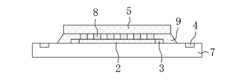
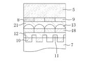
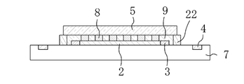
- an optical member such as a translucent substrate (translucent member) 5 attached to the semiconductor substrate 7 on which the effective pixel portion 2 is formed is referred to as a “solid-state imaging device”.
- the semiconductor substrate 7 used in the solid-state imaging device 1 of the present embodiment is plate-shaped, and its planar shape is, for example, a quadrilateral.
- the translucent substrate 5 is indicated by a chain line in FIG. 1 and covers the effective pixel portion 2 and the wiring portion 3 as a whole in plan view.
- symbol 6 shown in FIG. 1 represents a floating diffusion part.
- a quadrilateral effective pixel portion 2 At the center of the light receiving surface of the solid-state imaging device 1, there is provided a quadrilateral effective pixel portion 2 in which a plurality of light receiving portions are arranged in a matrix, and the four sides of the effective pixel portion 2 are opposed to each other. Outside the set of sides, a plurality of electrode pad portions 4 are arranged in a line along the side.
- the electrode pad unit 4 is provided for exchanging signals and the like with an external circuit, such as outputting a signal output from the effective pixel unit 2 to the outside.
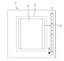
- the electrode pad portion 4 may be provided along four sides of the semiconductor substrate 7 as shown in FIG. 5, or provided along only one side of the semiconductor substrate 7 as shown in FIG. It may be done.
- FIG. 5 is a plan view showing a solid-state imaging device according to a first modification of the present embodiment
- FIG. 6 is a plan view showing a solid-state imaging device according to a second modification of the present embodiment. It is.
- a light-transmitting substrate 5 is bonded to a light-receiving surface of a semiconductor substrate 7 with a light-transmitting adhesive 9, and the semiconductor substrate 7.
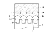
- a plurality of spacers (first spacers) 8 are provided between the effective pixel portion 2 and the translucent substrate 5. More specifically, the spacer 8 is provided above the effective pixel portion 2 and at a position directly below the translucent substrate 5. Since the spacer 8 is a characteristic part of the solid-state imaging device 1 of the present embodiment, it will be described in detail later.
- a light receiving portion 10 that performs photoelectric conversion is provided above the semiconductor substrate 7, and on a portion adjacent to the light receiving portion 10 of the semiconductor substrate 7.
- a transfer electrode 11 and the like are provided.
- a flattening layer 12 for flattening a step is formed on the transfer electrode 11, the semiconductor substrate 7, and the wiring part 3, and a microlens 13 and a spacer 8 are sequentially formed on the flattening layer 12.
- the semiconductor substrate 7 and the translucent substrate 5 are attached by a translucent adhesive 9.
- the translucent adhesive 9 is provided immediately above the microlens 13 and fills the space between the spacers 8.
- the solid-state imaging device 1 is a CCD (Charge-Coupled Device) type
- the solid-state imaging device 1 may be a MOS-type (Metal-Oxide Semiconductor).
- the solid-state imaging device 1 of this embodiment is mounted on a package substrate 14, and the electrode pad portion 4 is electrically connected to a lead terminal 15 installed on the package substrate 14 by a wire 16.
- a solid-state imaging device is obtained.
- a part of the lead terminal 15 is exposed to the outside of the package substrate 14 and serves as a terminal for connection to an external device.
- the exposed surface of the semiconductor substrate 7 and the wire 16 are sealed with a sealing resin 17.
- the solid-state imaging device of the present embodiment can also be applied to a case where the through electrode 30 (shown by a dotted line in FIG. 4) penetrating from the light receiving surface to the back surface of the semiconductor substrate 7 is provided.
- a flip-chip connection that connects the lead terminal 15 of the package substrate 14 without providing the wire 16 may be employed.
- the constituent material of the spacer 8 used in the solid-state imaging device of the present embodiment may be a material that is at least transparent to incident light, such as acrylic, styrene, phenol novolac, polyimide, or the like. It may be a positive or negative photosensitive resin, or an organic resin such as urethane, epoxy, styrene, or siloxane. When an organic resin is used, the spacer 8 can be formed without any trouble even after an organic film (such as the planarization layer 12) having low heat resistance is formed to form a color filter, a microlens, or the like. .
- a spherical, fiber-like or indeterminate filler such as resin, glass or quartz is contained in an amount of more than 0% and less than 3000% (weight percent) with respect to the binder resin. It may be used.
- the refractive index of the spacer 8 or the mechanical strength of the spacer 8 can be changed.
- the refractive index of the spacer 8 can be increased by containing a filler having a high refractive index such as titanium oxide (TiO 2 ) or zirconium oxide (ZrO 2 ).
- permeability of visible light in the spacer 8 can be lowered
- the translucent substrate 5 is composed of an inorganic material (such as borosilicate glass or quartz glass), an organic material (such as acrylic resin, polycarbonate resin, or olefin resin), or a hybrid (hybrid) thereof. That is, the translucent substrate 5 is preferably made of a material satisfying that it has a high visible light transmittance, can be processed into a flat plate shape, and can be bonded with a translucent adhesive 9 described later. . *
- an organic material is used as the material of the translucent substrate 5 and the impact resistance is not sufficient depending on the application, it is more preferable to use a hybrid material in which an inorganic material is added as a filler.
- borosilicate glass is used as the material of the translucent substrate 5
- scratches are less likely to occur during handling than when a resin or the like is used, and in terms of solvent resistance, scratch resistance, and cost during manufacturing, High merit can be obtained.
- quartz is used for the translucent substrate 5, it is hard to get a crack at the time of handling, and a higher merit can be obtained in solvent resistance and scratch resistance at the time of manufacture.
- FIG. 3 shows an example in which one type of microlens 13 is arranged between the semiconductor substrate 7 and the translucent substrate 5, but the microlens 13 directly below the translucent substrate 5 and the semiconductor substrate 7 are arranged.
- One or more types of microlenses may be disposed between them so that light passing through the two or more microlenses enters the light receiving unit (FIGS. 18A to 18D).
- FIG. 19 (a) to (c)). In this case, it is possible to improve the light collection efficiency of incident light and improve the sensitivity.
- planarizing layer 12 and the microlens 13 are made of different materials. However, the planarizing layer 12 and the microlens 13 are integrally formed of the same material. Also good.
- FIG. 7 is an enlarged cross-sectional view showing an effective pixel portion of a solid-state imaging device according to a third modification of the first embodiment.
- an organic film 21 for protecting the surface of the device may be formed on the microlens 13.
- the spacer 8 and the translucent adhesive 9 are formed on the organic film 21.
- a material harder than the microlens 13 is preferably used as the material of the organic film 21, and examples thereof include acrylic, fluorine, and silicone materials. According to this configuration, the solid-state imaging device can be hardly damaged, and reflection of incident light can be further reduced by appropriately selecting the refractive index of the organic film 21.
- the reflection at the interface between the organic film 21 and the microlens 13 can be suppressed by making the refractive index of the organic film 21 smaller than the refractive index of the microlens 13.
- the organic film 21 is effective even when one or more microlenses (intralayer lenses) are formed between each microlens 13 and the corresponding light receiving unit 10.
- a color filter 18 corresponding to the microlens 13 may be provided on the planarizing layer 12 and below the microlens 13. Thereby, colorization of an output image is realizable.
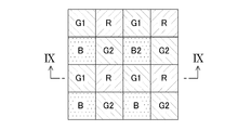
- FIG. 8 is a plan view schematically showing an arrangement example of color filters when a color filter is provided in the solid-state imaging device of the present embodiment
- FIG. 9 is a solid state according to a third modification of the present embodiment. It is sectional drawing in the IX-IX line
- the effective pixel portion shown in FIG. 8 is divided for each pixel having the respective light receiving portions 10.
- the primary color Bayer array composed of red (R), green (G1, G2), and blue (B) is used as the color filter array above the effective pixel unit 2. Etc. are used.
- the color filter 18 is disposed on the planarization layer 12 and at a position directly below the microlens 13, and is provided for each microlens 13. In the case where one or more microlenses (intralayer lenses) are formed between each microlens 13 and the corresponding light receiving unit 10, the color filter 18 is disposed, for example, immediately below the uppermost microlens. Is done.
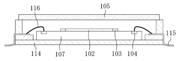
- FIG. 10 is a cross-sectional view showing a conventional solid-state imaging device having a hollow structure
- FIG. 11 is an enlarged cross-sectional view showing an effective pixel portion of the conventional solid-state imaging device shown in FIG. 10,
- FIG. It is an expanded sectional view showing an effective pixel part of a solid imaging device concerning one embodiment.
- the conventional solid-state imaging device includes a semiconductor substrate 107 on which an effective pixel portion 102, a wiring portion 103, and an electrode pad portion 104 are formed, and the semiconductor substrate 107.
- a package substrate 114 having a lead terminal 115 connected to 104 and a translucent substrate 105 disposed above the semiconductor substrate 107 are provided.
- reference numeral 110 denotes a light receiving portion
- reference numeral 111 denotes a transfer electrode
- reference numeral 112 denotes a flattening layer
- reference numeral 118 denotes a color filter.
- incident light 119 incident on the solid-state imaging device is reflected on the upper and rear surfaces of the translucent substrate 105 made of glass or the like, and on the upper surface of the microlens 113, and a loss corresponding to the reflected light 120 occurs. .
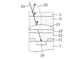
- the translucent substrate 5 is directly pasted on the effective pixel portion 2 of the semiconductor substrate 7 by the translucent adhesive 9. Since the translucent adhesive 9 having a refractive index larger than that of air is used, in the solid-state imaging device of the present embodiment, the difference in refractive index between the translucent substrate 5 and the translucent adhesive 9, and the micro The refractive index difference between the lens 13 and the translucent adhesive 9 can be reduced. For this reason, as shown in FIG. 12, the reflection of the light of the incident light 19 incident on the solid-state imaging device on the lower surface of the translucent substrate 5 and the upper surface of the microlens 13 is significantly larger than that of the conventional solid-state imaging device. The loss of light corresponding to the reflected light 20 can be reduced.
- the thickness of the solid-state imaging device can be reduced as compared with the conventional structure.
- the refractive index of the spacer 8 is larger than that of air, the reflection of light can be reduced in the pixel on which the spacer 8 is formed as compared with the conventional solid-state imaging device.
- the refractive index of the spacer 8 lower than the refractive index of the member (microlens 13 in the example shown in FIG. 12) located directly below the spacer 8
- FIGS. 2 and 3 another feature of the present embodiment is that, as shown in FIGS. 2 and 3, a spacer 8 is provided above the effective pixel portion 2 and immediately below the translucent substrate 5.
- a spacer 8 is provided above the effective pixel portion 2 and immediately below the translucent substrate 5.
- a light-transmitting adhesive 9 is applied to the semiconductor substrate 7 side or the light-transmitting substrate 5 side, and the semiconductor substrate 7 and the light-transmitting element 5 are transparent.
- the optical substrate 5 is bonded.
- the translucent adhesive 9 can be made difficult to flow out of the effective pixel portion 2 by the spacer 8, and therefore, if the height, arrangement, shape, etc. of the electrode pad portion 4 are appropriately selected, the outside of the effective pixel portion 2.
- the spacer for blocking the flow of the light-transmitting adhesive is not provided on the semiconductor substrate 7, it is possible to prevent the light-transmitting adhesive 9 from flowing on the electrode pad portion 4. Therefore, it is possible to prevent a connection failure or the like in the electrode pad portion 4, and it is not necessary to provide a region for forming a spacer outside the effective pixel portion 2, and the element can be reduced in size. Further, if the space between the spacers 8 is appropriately spaced or the shape of the spacers 8 is appropriately set as will be described later, the translucent adhesive 9 can be evenly distributed in the effective pixel portion 2, and the spacers 8. It is also possible to prevent problems such as air bubbles entering between them.
- the solid-state imaging device it is possible to suppress the occurrence of defects such as poor connection in the electrode pad portion 4 while reducing the size and the thickness. Further, since the upper surface of the spacer 8 is flat and substantially parallel to the upper surface of the semiconductor substrate 7, it is possible to prevent the translucent substrate 5 from being inclined when the translucent substrate 5 is bonded. For this reason, it is possible to prevent deterioration in image quality such as luminance unevenness (luminance shading) that occurs when the translucent substrate 5 is attached.
- the refractive index of the spacer 8 and the refractive index of the translucent adhesive 9 may be the same or different from each other. The effect in each case will be described below with reference to the drawings.
- FIG. 13A is an enlarged cross-sectional view showing an effective pixel portion when the refractive index of the spacer 8 is larger than that of the translucent adhesive 9 in the solid-state imaging device of the present embodiment
- FIG. 8 is an enlarged cross-sectional view showing an effective pixel portion when the refractive index of 8 is equal to the refractive index of the translucent adhesive 9
- (c) is a case where the refractive index of the spacer 8 is smaller than the translucent adhesive 9.
- It is an expanded sectional view which shows the effective pixel part.
- the spacer 8 can function as an optical waveguide. For this reason, in the pixel in which the spacer 8 is formed, the sensitivity can be selectively improved. As will be described later, the density of the spacers 8 functioning as optical waveguides is high in the peripheral portion of the effective pixel portion and low in the central portion of the effective pixel portion. Sensitivity can be improved and the brightness of the output image can be made uniform over the entire screen. (2) When the refractive index of the spacer 8 is equal to the refractive index of the translucent adhesive 9 In this case, as shown in FIG. It goes straight without being refracted at the interface with the adhesive 9 and enters the microlens 13.
- the optical characteristics do not change no matter how the spacers 8 are arranged in the effective pixel portion, so that the light is not refracted on the side surfaces of the spacers 8 and deterioration of the optical characteristics can be prevented.
- the spacer 8 may be provided across a plurality of adjacent pixels, or the spacer 8 may be formed on a part of the microlens 13.
- the location where the spacer 8 is formed in the solid-state imaging device of the present embodiment is not limited as long as it is within the effective pixel portion in principle, but the spacer 8 may be regularly arranged.
- the spacers 8 may be arranged only on pixels of a specific color. Specifically, when the spacer 8 is disposed only on the red pixel (R), disposed on only one or both of the green pixels (G1, G2), or disposed only on the blue pixel (B), There are cases where the arrangements are combined. Since the processing of the signal output from the solid-state imaging device is often performed for each pixel color, when the refractive index of the spacer 8 is different from the refractive index of the translucent adhesive 9, the spacer 8 is set for each specific pixel. By providing, signal processing can be facilitated. As will be described later in (2) of the third embodiment, this configuration is particularly effective for a CCD type solid-state imaging device.
- the spacer 8 is formed only on the green pixel, so that a solid with respect to green light having the highest human visibility is obtained. Since the sensitivity of the image sensor can be improved, the resolution can be improved.
- the refractive index of the spacer 8 is smaller than the refractive index of the translucent adhesive 9, for example, the sensitivity of the green pixel surrounded by the spacer 8 is improved by forming the spacer 8 in a red pixel and a blue pixel. Can be made.
- the color of the color filter 18 may be a complementary color system (cyan, magenta, yellow) or the like in addition to the primary color system described above, and the spacer 8 may be formed by only one color pixel or a plurality of colors. It may be within a color pixel.
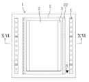
- FIG. 14 is a plan view showing a solid-state imaging device according to the second embodiment of the present invention.
- the solid-state imaging device of this embodiment is that a spacer (third spacer) 22 is provided on a portion of the semiconductor substrate 7 located outside the effective pixel portion 2. This is different from the solid-state imaging device of the first embodiment shown in FIG. Therefore, the description of the same configuration as that of the solid-state imaging device of the first embodiment is omitted, and mainly the characteristic portion will be described.
- a solid-state image sensor is required to be downsized.
- an imaging apparatus such as a single-lens reflex camera, it is required to make the solid-state image sensor large and thin while focusing on image quality.
- FIGS. 15A to 15C are cross-sectional views showing a method for manufacturing a solid-state imaging device according to a reference example
- FIG. 16 shows a solid-state imaging device according to the second embodiment shown in FIG. It is sectional drawing in a XVI-XVI line.
- a liquid translucent adhesive 109 is applied on the effective pixel portion 102.
- the translucent substrate 105 is placed on the semiconductor substrate 107 and lightly pressed.
- the spacers 122 are provided outside the effective pixel unit 102 and in a partition shape along a pair of sides of the effective pixel unit 102 that face each other.
- the spacer 122 By providing the spacer 122, when the translucent substrate 105 is bonded to the semiconductor substrate 107, the flow of the translucent adhesive 109 is blocked by the spacer 122, so that the translucent adhesive 109 is formed on the electrode pad portion 104. Can be prevented from flowing. However, as shown in FIG. 15C, when the translucent adhesive 109 is cured, the translucent adhesive 109 contracts and the translucent substrate 5 bends (if the spacing between the spacers 122 is wide). )).
- the solid-state imaging device of the present embodiment as shown in FIG. 16, spacers 22 arranged in parallel to each other are provided outside the effective pixel unit 2 and the effective pixel unit 2 is formed. Since the spacer 8 is provided in the planar region, it is possible to suppress the light-transmitting substrate 5 from being bent in the bonding process of the light-transmitting substrate 5, and to suppress deterioration of optical characteristics and the like. As described above, in the solid-state imaging device of the present embodiment, it is possible to suppress the occurrence of poor connection and the deterioration of optical characteristics while realizing thinning.
- the thickness of the translucent substrate 5 is not limited to 100 ⁇ m, and the configuration of the present embodiment is particularly effective within a range of, for example, several tens of ⁇ m to 500 ⁇ m.
- the interval between the parallel spacers 22 is, for example, the same as the pixel pitch (several ⁇ m) or an integer multiple thereof, and the length of one side of the semiconductor substrate 7 is, for example, about 10 mm to several tens mm.
- the height of the spacer 8 is preferably about the same as the height of the spacer 22, and is about several ⁇ m to 50 ⁇ m, for example.
- the formation pattern of the spacers 8 provided immediately below the translucent substrate 5 for example, the following can be considered.
- the deflection of the translucent substrate 5 is larger on the central portion than on the peripheral portion of the effective pixel portion 2, but the total area of the spacer 8 on the central portion of the effective pixel portion 2 is Since it is larger than the total area on the peripheral portion, the load resistance is improved and the deflection of the translucent substrate 5 is suppressed.
- the density of the spacers 8 refers to the number of spacers 8 per unit area.
- (2) Pattern in which the spacers 8 are uniformly formed on the entire effective pixel portion 2 This pattern corresponds to the case where the spacers 8 are provided for pixels of a specific color as described in the first embodiment. As described above, in this case, the sensitivity at a desired pixel can be improved. In particular, in the case of a CCD type solid-state imaging device, signal readout control cannot be performed for each pixel, and the signal is corrected for each color. Therefore, if the spacers 8 are regularly formed in the region where the effective pixel portion 2 is formed, the influence of the spacers 8 on the optical characteristics can be corrected by signal processing even in the CCD solid-state imaging device. .
- the translucent adhesive 9 can be uniformly distributed over the effective pixel portion 2 as a whole.
- (3) Pattern in which the density of the spacers 8 on the effective pixel portion 2 is low on the central portion of the effective pixel portion 2 and high on the peripheral portion, as described in the first embodiment, the spacer 8 or the spacer 8 By using this pattern when the translucent adhesive 9 surrounded by is used as an optical waveguide, it is possible to improve the sensitivity in the peripheral portion of the effective pixel portion 2 with less incident light than in the central portion. . Thereby, the image quality can be improved.
- the translucent adhesive 9 is applied to the effective pixel portion. It spreads quickly within 2.
- the translucent adhesive 9 can be quickly spread in the effective pixel portion 2 in the bonding step, and an area outside the effective pixel portion 2 (electrode pad portion). 4 and the like) can prevent the translucent adhesive 9 from protruding.
- the density of the spacers 8 may be changed steeply (non-linearly) from the center of the effective pixel portion 2 toward the peripheral portion, or gradually ( (Linear).
- the spacer 8 may be formed at a random position.
- the cross-sectional shape of the spacer 8 in the direction horizontal to the main surface of the semiconductor substrate may be circular or polygonal.
- the translucent substrate 5 is placed on the semiconductor substrate 7, and the spacer 8 does not easily block the flow of the translucent adhesive 9 when pressed, so that the translucent substrate is placed on the semiconductor substrate 7. 5 can be stuck without gaps.
- this effect becomes remarkable when the horizontal cross section of the spacer 8 is circular.
- the fourth embodiment of the present invention includes an OB (Optical Black) portion provided adjacent to the effective pixel portion 2, and a spacer made of a light shielding material is disposed as a light shielding film above the OB portion. It is characterized by that.
- OB Optical Black
- each pixel in the region where the OB portion is formed has a light receiving portion 10, a transfer electrode 11, a planarizing layer 12, and a microlens 13 (see FIGS. 3, 7, and 9).
- noise dark current
- the microlens 13 is covered with a light-shielding spacer (second spacer) in the entire region where the OB portion is formed.
- This light-shielding spacer is made of a resin obtained by mixing carbon, organic or inorganic pigments with the resin mentioned above as the material of the spacer 8.
- This light blocking spacer may be provided alone or in combination with the spacer 8 on the effective pixel portion 2.
- a wiring made of metal is often formed as a light shielding film above the OB portion (see FIGS. 18A to 18C, etc.).
- the wiring needs to be thick, a step is generated between the effective pixel portion and the wiring portion during manufacturing. Therefore, the planarizing layer 12 and the like are formed above the substrate in order to fill this step.
- the thickness of the solid-state imaging device of this embodiment and the solid-state imaging device equipped with the same can be greatly reduced.
- FIG. 17 is a flowchart showing manufacturing steps of the solid-state imaging device according to the fifth embodiment of the present invention.
- FIGS. 18A to 18D and FIGS. 19A to 19C are cross-sectional views of the solid-state imaging device in main steps among the steps shown in FIG.
- a manufacturing method in the case where the color filter 18, the intralayer lens 23, and the organic film 21 are provided in the solid-state imaging device of the first embodiment will be described as an example.
- 18 (a) to 18 (d) and 19 (a) to 19 (c) the left figure shows a cross section passing through the wiring part 3 and the floating diffusion part 6, and the right figure shows the light receiving part 10 and the microlens 13. The cross section which passes etc. is shown.
- a light receiving portion 10, a floating diffusion portion 6 and the like are formed on an upper portion of a wafer-like semiconductor substrate 7 by a known diffusion process.
- a transfer electrode 11 having a predetermined shape is formed on the semiconductor substrate 7, and then an in-layer lens 23 is formed on the light receiving unit 10 of the semiconductor substrate 7.
- the constituent material is applied while the semiconductor substrate 7 is rotated, and then a photolithography process or the like is performed to form the inner lens 23 having a convex upper surface.
- the constituent material of the in-layer lens 23 may be a translucent resin or an inorganic material such as SiN.
- the first-layer wiring portion 3 is formed at a predetermined position on the semiconductor substrate 7.
- the electrode pad portion 4 may be formed simultaneously with the wiring portion 3.
- the height of the upper surface of the wiring portion 3 is higher than the upper surface of the in-layer lens 23.
- the height of the wiring portion 3 is It can be equal or less. Further, this step is not necessary when forming a solid-state imaging device having no intralayer lens 23 as shown in FIG.
- a light-transmitting resin or the like is applied while the semiconductor substrate 7 is rotated, and photolithography or the like is performed to flatten the inner lens 23 or the wiring portion 3. Then, a step is formed on the upper surface of the substrate (solid imaging device being manufactured).
- the color filter 18 is formed on a portion of the planarizing layer 12 located above the effective pixel portion 2 by a known method, and the microlens 13 is formed on the color filter 18.
- an organic film 21 is formed on the microlens 13 above the effective pixel portion 2 and on the planarizing layer 12 on the wiring portion 3.
- portions of the organic film 21, the planarization layer 12, and the like formed on the floating diffusion portion 6 are removed by etching or the like.
- portions of the organic film 21 and the planarizing layer 12 formed on the electrode pad portion 4 are also removed by etching or the like in the same manner as the portion on the floating diffusion portion 6.
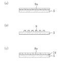
- the constituent material of the spacer 8 is applied to the entire surface of the substrate to form the spacer material film 8a.
- the constituent material is applied while rotating the semiconductor substrate 7 (rotary application method).
- photolithography processing or the like is performed on the spacer material film 8a to cure the portion that becomes the spacer 8 in the spacer material film 8a and to peel off the other portions.
- the spacer 8 is formed above the effective pixel portion 2.
- the constituent material of the spacer 8 may be a material transparent to at least incident light.
- acrylic, styrene, phenol novolac, polyimide, or the like, or a general positive type or negative type is used. It may be a photosensitive resin or an organic resin such as urethane, epoxy, styrene, or siloxane.
- a spherical, fiber-like or indeterminate filler such as resin, glass or quartz is contained in an amount of more than 0% and less than 3000% (weight percent) with respect to the binder resin. It may be used.
- the refractive index of the spacer 8 or the mechanical strength of the spacer 8 can be changed.
- the refractive index of the spacer 8 can be increased by containing a filler having a high refractive index such as titanium oxide (TiO 2 ) or zirconium oxide (ZrO 2 ).
- the transmittance of visible light in the spacer 8 may be lowered by incorporating carbon, an organic or inorganic pigment into the resin.
- the thickness of the spacer 8 can be arbitrarily set, and if the thickness of the spacer material film 8a is about 1 to 50 ⁇ m, the spacer material film 8a can be formed by one spin coating (spin coating). When the spacer material film 8a is thicker than this, the spin coating is performed a plurality of times. Also, by using the spin coating method, the upper surface of the semiconductor substrate 7 and the upper surface of the coating film can be made substantially parallel. Then, the spacer 8 can be formed by leaving a predetermined part of the spacer material film 8a and removing the other part. If the spacer material film 8a is thick, it may be formed by die coating.
- the spacer 8 is made of a photosensitive resin
- the portion to be the spacer 8 is cured by photolithography and unnecessary portions are peeled off.
- the rotational speed during spin coating is about 1000 rpm to 3000 rpm
- the prebake temperature is about 80 ° C. to 100 ° C.
- the exposure time is about 100 msec to 1000 msec
- the developer is an alkaline developer or an organic developer.
- the spacer 8 is made of an etchable resin
- a resist mask in which an opening is formed on the other part of the resin film after the resin film is formed is usually covered.
- the lithography process is used.
- a portion that becomes the spacer 8 is left by etching and an unnecessary portion is removed.
- a translucent adhesive 9 is applied to a region of the semiconductor substrate 7 corresponding to the light receiving unit 10.
- the translucent adhesive 9 for example, an epoxy adhesive that cures at about 100 ° C. to 150 ° C., or a silicone adhesive that cures at room temperature to about 150 ° C. is used.
- a method for applying the translucent adhesive 9 for example, a dispensing method is used.
- the translucent adhesive 9 means an adhesive having translucency after curing.
- the translucent substrate 5 is adhered to the semiconductor substrate 7.
- the translucent substrate 5 is placed on the semiconductor substrate 7 to which the translucent adhesive 9 is applied, and the translucent adhesive 9 is translucent within a period in which the translucent adhesive 9 is fluid.
- the substrate 5 is pressed until it contacts the upper surface of the spacer 8. While pressing the translucent substrate 5 or after pressing, the translucent substrate 5 is shifted in the horizontal direction to adjust the horizontal position and tilt of the translucent substrate 5.
- the semiconductor substrate 7 is preferably sealed with the package substrate 14, the translucent substrate 5, and the translucent adhesive 9.
- the translucent adhesive 9 wraps around the spacer 8 and seals the semiconductor substrate 7 when the translucent substrate 5 is attached.
- the application amount and application location of the adhesive 9 are adjusted in advance. Care must be taken so that the translucent transparent adhesive 9 does not reach the region corresponding to the floating diffusion portion 6 formed on the semiconductor substrate 7. Thereafter, the translucent adhesive 9 is cured in a state where the translucent substrate 5 is in contact with the upper surface of the spacer 8.
- a solid-state imaging device can be formed by bonding the electrode pad portion 4 and the lead terminal 15 with a wire.
- the semiconductor substrate 7 and the light-transmitting device are used. It is possible to prevent the conductive substrate 5 from being bent due to the shrinkage accompanying the curing of the translucent adhesive. Further, the translucent adhesive 9 applied to the region corresponding to the light receiving portion 10 on the semiconductor substrate 7 can be prevented from flowing into the region corresponding to the floating diffusion portion 6. By doing so, the sensitivity of the solid-state imaging device can be increased by several% to 10%.
- the thickness of the translucent adhesive 9 can be set to a desired thickness.
- the height of the upper surface of the spacer 8 is higher than the height of the top of the microlens 13. That is, a gap exists between the translucent substrate and the uppermost surface of a member formed on the semiconductor substrate 7 such as the microlens 13.
- the spacer 8 also serves to prevent the microlens 13 from being crushed.
- the spacer 8 is not limited to a place where the spacer 8 is not provided, but also is a place where the spacer 8 is provided.
- the translucent substrate 5 can be prevented from crushing the microlenses 13 and the like.
- the spacer 8 since the upper surface of the spacer 8 is substantially parallel to the upper surface of the semiconductor substrate 7, the light-transmitting substrate 5 is stuck to the upper surface of the spacer 8 so that the light-transmitting substrate 5 is adhered. 5 can be attached to the semiconductor substrate 7 substantially in parallel.
- the spacer 8 exists over almost the entire surface of the effective pixel unit 2. Therefore, in the solid-state imaging device according to the first embodiment, the translucent substrate 5 can be attached to the semiconductor substrate 7 substantially in parallel. As a result, it is possible to prevent image quality degradation such as luminance unevenness (luminance shading) that occurs when the translucent substrate 5 is attached to the semiconductor substrate 7.
- the spacer 8 is formed in the wafer process (process before dividing into chips), it is possible to suppress variations in the height of the spacer 8 for each product.
- the entire solid-state imaging device can be reduced in size and thickness. Furthermore, since the microlens 13 does not come into contact with air after the translucent substrate 5 is bonded, it is possible to prevent deterioration of the shape, transparency, and refractive index of the microlens 13 due to changes in the surrounding environment such as humidity. This effect becomes significant when the microlens 13 is made of a transparent resin.
- the spacer material film 8a when forming the spacer material film 8a, a die coating method, vapor deposition, or a dry process such as sputtering may be used in addition to the method of spin coating the constituent materials.
- the patterning of the spacer 8 can also be performed by photolithography, nanoimprinting, or the like when using a photosensitive resin. According to these methods, since it is not necessary to form an etching mask as compared with a method using etching, the manufacturing process can be simplified.
- the spacer 8 when the spacer 8 is made of a material other than the photosensitive resin, it can be performed by a lift-off method, a dry etching method, an ink jet method, or the like. When dry etching is used, the range of selection of materials can be expanded as compared with the case where photosensitive materials are used.
- the flow of the translucent adhesive 9 is poor in a region surrounded on all sides by the spacer 8. Therefore, it is preferable to apply the translucent adhesive 9 using a spray.
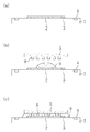
- FIGS. 21 (a) to 21 (c) are cross-sectional views showing a process for manufacturing a solid-state imaging device in the method for manufacturing a solid-state imaging device according to the sixth embodiment of the present invention.
- a resin material constituting the spacer 8 is spin-coated on the translucent substrate 5 to form a spacer material film 8a.
- the thickness of the spacer material film 8a is, for example, about 1 to 50 ⁇ m, it can be formed by one spin coating.
- the material used for the spacer 8 is made of resin, for example.
- the spacer 8 is made of a general positive or negative photosensitive resin such as acrylic, styrene, phenol novolac, or polyimide, or an organic resin such as urethane, epoxy, styrene, or siloxane. It can be used as a material.
- the spacer 8 is formed on the light-transmitting substrate 5 by removing a part of the spacer material film 8a using lithography or the like and leaving a desired part.
- the base layer 24 is formed on the light-transmitting substrate 5 for the purpose of improving the adhesion between the spacer 8 and the light-transmitting substrate 5.
- the spacer material film 8a may be formed.
- the material of the underlayer 24 include organic materials such as HMDS (1,1,1,3,3,3-hexamethyldisilazane) and acrylic, and silicon oxide (SiO 2 ).
- the spacer 8 may be formed after the transparent substrate 5 is cut into a size corresponding to each solid-state imaging element in advance, or after the spacer 8 is formed on the large transparent substrate 5. Alternatively, a size corresponding to each solid-state image sensor may be cut by performing a dicing process or the like.
- the translucent adhesive 9 is applied on the effective pixel portion 2 of the semiconductor substrate 7, the surface on which the spacer 8 is formed is formed on the semiconductor.
- the translucent substrate 5 is placed on the effective pixel portion 2 of the semiconductor substrate 7 in a state facing the substrate 7.
- the translucent adhesive agent 9 is hardened in the state which pressed the translucent board
- light such as ultraviolet rays or visible light may be irradiated, a temperature of about 100 to 200 ° C. may be applied, and light and heat may be used in combination. .
- the constituent material of the spacer 8 and the translucent adhesive 9 may be the same.
- the translucent substrate 5 on which the spacer 8 is formed is attached to the semiconductor substrate 7, the uppermost surface of the substrate on the effective pixel portion 2 (the surface serving as an adhesive surface with the spacer 8) is flat. desirable.
- the spacer 8 is present when the translucent substrate 5 is attached to the semiconductor substrate 7, the translucent substrate 5 is contracted by the curing of the translucent adhesive 9. It is possible to prevent bending. Further, the translucent adhesive 9 applied to the region corresponding to the light receiving portion 10 on the semiconductor substrate 7 can be prevented from flowing into the region corresponding to the floating diffusion portion 6. By doing so, it is possible to increase the sensitivity of the solid-state imaging device and the solid-state imaging device on which the solid-state imaging device is mounted by several% to 10%.
- the translucent substrate 5 is stuck in a pressed state until the end surface of the spacer 8 is in contact with the upper surface of the substrate (the portion on the semiconductor substrate 7 side of the solid-state imaging device being formed).
- the distance from the conductive substrate 5, that is, the thickness of the translucent adhesive 9 is defined by the height of the spacer 8. Therefore, the thickness of the translucent adhesive 9 can be set to a desired thickness by setting the spacer 8 to a desired height.
- the translucent substrate 5 is attached to the end surface of the spacer 8 with the semiconductor substrate 7 being in contact with the substrate surface of the semiconductor substrate 7.
- they can be attached almost in parallel.
- the spacers 8 are present on almost the entire surface of the effective pixel unit 2. Therefore, the translucent substrate 5 can be attached to the semiconductor substrate 7 almost in parallel with relatively high accuracy. Therefore, it is possible to prevent deterioration in image quality such as luminance unevenness (luminance shading) that occurs when the translucent substrate 5 is attached to the semiconductor substrate 7 while being inclined.
- the size of the solid-state imaging device, and thus the entire solid-state imaging device can be reduced. Can be thinned. Furthermore, it is possible to prevent the shape, transparency, and refractive index of the microlens 13 from being deteriorated due to changes in the surrounding environment such as humidity.
- a die coating method, vapor deposition, or a dry process such as sputtering may be used in addition to the method of spin coating the constituent materials.
- the patterning of the spacer 8 can also be performed by photolithography, nanoimprinting, or the like when using a photosensitive resin.
- a lift-off method, a dry etching method, an ink jet method or the like may be used.
- the solid-state imaging device and the solid-state imaging device according to the present invention can be used for various imaging devices such as a digital camera and a video camera.
Landscapes
- Physics & Mathematics (AREA)
- General Physics & Mathematics (AREA)
- Optics & Photonics (AREA)
- Solid State Image Pick-Up Elements (AREA)
- Structures Or Materials For Encapsulating Or Coating Semiconductor Devices Or Solid State Devices (AREA)
- Transforming Light Signals Into Electric Signals (AREA)
Abstract
La présente invention a trait à un élément capteur d’image à semi-conducteurs comprenant : un substrat semi-conducteur (7) dans lequel une partie de pixel effective (2) contenant une pluralité de parties de réception de lumière (10) est formée ; des entretoises (8) formées sur la partie de pixel effective (2) ; un adhésif transmettant la lumière (9) qui remplit les espaces entre les entretoises (8) ; et un substrat transmettant la lumière (5) qui est lié au moyen de l’adhésif transmettant la lumière (9) sur les entretoises (8) et qui, suivant une vue en plan, recouvre la partie de pixel effective (2). Une partie d’électrode (4) est formée sur une région du substrat semi-conducteur (7) du côté extérieur de la partie de pixel effective (2).
Priority Applications (1)
| Application Number | Priority Date | Filing Date | Title |
|---|---|---|---|
| US12/783,086 US20100224948A1 (en) | 2008-07-03 | 2010-05-19 | Solid-state imaging element, method for fabricating the same, and solid-state imaging device |
Applications Claiming Priority (2)
| Application Number | Priority Date | Filing Date | Title |
|---|---|---|---|
| JP2008174660A JP2010016173A (ja) | 2008-07-03 | 2008-07-03 | 固体撮像素子、その製造方法、及び固体撮像装置 |
| JP2008-174660 | 2008-07-03 |
Related Child Applications (1)
| Application Number | Title | Priority Date | Filing Date |
|---|---|---|---|
| US12/783,086 Continuation US20100224948A1 (en) | 2008-07-03 | 2010-05-19 | Solid-state imaging element, method for fabricating the same, and solid-state imaging device |
Publications (1)
| Publication Number | Publication Date |
|---|---|
| WO2010001524A1 true WO2010001524A1 (fr) | 2010-01-07 |
Family
ID=41465633
Family Applications (1)
| Application Number | Title | Priority Date | Filing Date |
|---|---|---|---|
| PCT/JP2009/002259 Ceased WO2010001524A1 (fr) | 2008-07-03 | 2009-05-21 | Elément capteur d’image à semi-conducteurs, son procédé de fabrication et dispositif capteur d’image à semi-conducteurs |
Country Status (3)
| Country | Link |
|---|---|
| US (1) | US20100224948A1 (fr) |
| JP (1) | JP2010016173A (fr) |
| WO (1) | WO2010001524A1 (fr) |
Cited By (1)
| Publication number | Priority date | Publication date | Assignee | Title |
|---|---|---|---|---|
| JP2016025404A (ja) * | 2014-07-17 | 2016-02-08 | 株式会社リコー | 撮像ユニット、画像読取装置および画像形成装置 |
Families Citing this family (9)
| Publication number | Priority date | Publication date | Assignee | Title |
|---|---|---|---|---|
| JP5287763B2 (ja) * | 2010-02-24 | 2013-09-11 | 株式会社デンソー | センサ装置およびその製造方法 |
| JP6056186B2 (ja) * | 2012-05-08 | 2017-01-11 | 株式会社ニコン | 撮像素子 |
| JP6065470B2 (ja) * | 2012-08-31 | 2017-01-25 | セイコーエプソン株式会社 | 撮像装置、検査装置、及び電子デバイスの製造方法 |
| JP6065508B2 (ja) * | 2012-10-05 | 2017-01-25 | セイコーエプソン株式会社 | 撮像装置の製造方法 |
| JP6071612B2 (ja) * | 2013-02-14 | 2017-02-01 | ナミックス株式会社 | 液状樹脂組成物、フリップチップ実装体およびその製造方法 |
| KR20140126598A (ko) * | 2013-04-23 | 2014-10-31 | 삼성전자주식회사 | 반도체 패키지 및 그 제조 방법 |
| JP6295983B2 (ja) | 2015-03-05 | 2018-03-20 | ソニー株式会社 | 半導体装置およびその製造方法、並びに電子機器 |
| JP6427691B2 (ja) * | 2016-11-30 | 2018-11-21 | 株式会社ダイセル | 撮像装置用レンズモジュール及びその製造方法 |
| US20210159373A1 (en) * | 2019-11-22 | 2021-05-27 | Facebook Technologies, Llc | Light extraction for micro-leds |
Citations (5)
| Publication number | Priority date | Publication date | Assignee | Title |
|---|---|---|---|---|
| JPH0281064U (fr) * | 1988-12-12 | 1990-06-22 | ||
| JP2001292363A (ja) * | 2000-04-10 | 2001-10-19 | Mitsubishi Electric Corp | 撮像装置および携帯電話機 |
| JP2002261260A (ja) * | 2001-02-28 | 2002-09-13 | Nikon Corp | 固体撮像装置 |
| JP2006278877A (ja) * | 2005-03-30 | 2006-10-12 | Canon Inc | 放射線撮像装置及びその製造方法 |
| JP2007110117A (ja) * | 2005-10-10 | 2007-04-26 | Samsung Electro Mech Co Ltd | イメージセンサのウエハレベルチップスケールパッケージ及びその製造方法 |
Family Cites Families (8)
| Publication number | Priority date | Publication date | Assignee | Title |
|---|---|---|---|---|
| JPH11142844A (ja) * | 1997-11-07 | 1999-05-28 | Canon Inc | 液晶表示装置 |
| US6603107B2 (en) * | 2000-04-10 | 2003-08-05 | Mitsubishi Denki Kabushiki Kaisha | Image pickup device and portable telephone |
| JP3675402B2 (ja) * | 2001-12-27 | 2005-07-27 | セイコーエプソン株式会社 | 光デバイス及びその製造方法、光モジュール、回路基板並びに電子機器 |
| US6894840B2 (en) * | 2002-05-13 | 2005-05-17 | Sony Corporation | Production method of microlens array, liquid crystal display device and production method thereof, and projector |
| JP4097508B2 (ja) * | 2002-11-19 | 2008-06-11 | シャープ株式会社 | マイクロレンズ基板の作製方法およびマイクロレンズ露光光学系 |
| JP4469781B2 (ja) * | 2005-07-20 | 2010-05-26 | パナソニック株式会社 | 固体撮像装置及びその製造方法 |
| JP2007097985A (ja) * | 2005-10-07 | 2007-04-19 | Aruze Corp | 遊技機及び遊技システム |
| US7729055B2 (en) * | 2008-03-20 | 2010-06-01 | Aptina Imaging Corporation | Method and apparatus providing concave microlenses for semiconductor imaging devices |
-
2008
- 2008-07-03 JP JP2008174660A patent/JP2010016173A/ja not_active Withdrawn
-
2009
- 2009-05-21 WO PCT/JP2009/002259 patent/WO2010001524A1/fr not_active Ceased
-
2010
- 2010-05-19 US US12/783,086 patent/US20100224948A1/en not_active Abandoned
Patent Citations (5)
| Publication number | Priority date | Publication date | Assignee | Title |
|---|---|---|---|---|
| JPH0281064U (fr) * | 1988-12-12 | 1990-06-22 | ||
| JP2001292363A (ja) * | 2000-04-10 | 2001-10-19 | Mitsubishi Electric Corp | 撮像装置および携帯電話機 |
| JP2002261260A (ja) * | 2001-02-28 | 2002-09-13 | Nikon Corp | 固体撮像装置 |
| JP2006278877A (ja) * | 2005-03-30 | 2006-10-12 | Canon Inc | 放射線撮像装置及びその製造方法 |
| JP2007110117A (ja) * | 2005-10-10 | 2007-04-26 | Samsung Electro Mech Co Ltd | イメージセンサのウエハレベルチップスケールパッケージ及びその製造方法 |
Cited By (1)
| Publication number | Priority date | Publication date | Assignee | Title |
|---|---|---|---|---|
| JP2016025404A (ja) * | 2014-07-17 | 2016-02-08 | 株式会社リコー | 撮像ユニット、画像読取装置および画像形成装置 |
Also Published As
| Publication number | Publication date |
|---|---|
| US20100224948A1 (en) | 2010-09-09 |
| JP2010016173A (ja) | 2010-01-21 |
Similar Documents
| Publication | Publication Date | Title |
|---|---|---|
| WO2010001524A1 (fr) | Elément capteur d’image à semi-conducteurs, son procédé de fabrication et dispositif capteur d’image à semi-conducteurs | |
| TWI394269B (zh) | 電子元件晶圓模組、電子元件晶圓模組之製造方法、電子元件模組及電子資訊裝置 | |
| CN101606381B (zh) | 在利用光学堆栈的照相机系统中的杂散光控制及相关方法 | |
| US7923798B2 (en) | Optical device and method for fabricating the same, camera module using optical device, and electronic equipment mounting camera module | |
| JP5489543B2 (ja) | 固体撮像装置 | |
| CN100354883C (zh) | 图像拾取装置及其生产方法 | |
| JP5009209B2 (ja) | ウエハ状光学装置およびその製造方法、電子素子ウエハモジュール、センサウエハモジュール、電子素子モジュール、センサモジュール、電子情報機器 | |
| JP4469781B2 (ja) | 固体撮像装置及びその製造方法 | |
| US20100117176A1 (en) | Camera module and manufacturing method thereof | |
| JP2003204053A (ja) | 撮像モジュール及び該撮像モジュールの製造方法、デジタルカメラ | |
| CN107919371B (zh) | 光电转换装置和系统 | |
| JP2006228837A (ja) | 半導体装置及びその製造方法 | |
| KR100705349B1 (ko) | 고체촬상장치, 반도체 웨이퍼 및 카메라 모듈 | |
| CN111758165A (zh) | 固态摄像装置和固态摄像器件 | |
| JP2007142207A (ja) | 固体撮像装置及びその製造方法 | |
| JP7700319B2 (ja) | 表示装置、モジュールおよび機器 | |
| JP2010165939A (ja) | 固体撮像装置及びその製造方法 | |
| JP4528879B2 (ja) | 固体撮像装置及びその製造方法 | |
| JP2011187482A (ja) | 固体撮像装置、光学装置用モジュール、及び固体撮像装置の製造方法 | |
| JP2009251249A (ja) | ウエハ状光学装置およびその製造方法、電子素子ウエハモジュール、センサウエハモジュール、電子素子モジュール、センサモジュール、電子情報機器 | |
| TW201944585A (zh) | 光學感測器及其形成方法 | |
| JP2008166779A (ja) | イメージセンサー及びその製造方法 | |
| JP4521938B2 (ja) | 撮像装置 | |
| JP2007150266A (ja) | 固体撮像装置の製造方法、及び固体撮像装置 | |
| JP2013161873A (ja) | 固体撮像装置及びカメラモジュール |
Legal Events
| Date | Code | Title | Description |
|---|---|---|---|
| 121 | Ep: the epo has been informed by wipo that ep was designated in this application |
Ref document number: 09773102 Country of ref document: EP Kind code of ref document: A1 |
|
| NENP | Non-entry into the national phase |
Ref country code: DE |
|
| 122 | Ep: pct application non-entry in european phase |
Ref document number: 09773102 Country of ref document: EP Kind code of ref document: A1 |