WO2010001754A1 - Préimprégné pour carte imprimée et carte imprimée - Google Patents
Préimprégné pour carte imprimée et carte imprimée Download PDFInfo
- Publication number
- WO2010001754A1 WO2010001754A1 PCT/JP2009/061321 JP2009061321W WO2010001754A1 WO 2010001754 A1 WO2010001754 A1 WO 2010001754A1 JP 2009061321 W JP2009061321 W JP 2009061321W WO 2010001754 A1 WO2010001754 A1 WO 2010001754A1
- Authority
- WO
- WIPO (PCT)
- Prior art keywords
- fiber
- polybenzazole
- prepreg
- printed wiring
- wiring board
- Prior art date
- Legal status (The legal status is an assumption and is not a legal conclusion. Google has not performed a legal analysis and makes no representation as to the accuracy of the status listed.)
- Ceased
Links
Images






Classifications
-
- H—ELECTRICITY
- H05—ELECTRIC TECHNIQUES NOT OTHERWISE PROVIDED FOR
- H05K—PRINTED CIRCUITS; CASINGS OR CONSTRUCTIONAL DETAILS OF ELECTRIC APPARATUS; MANUFACTURE OF ASSEMBLAGES OF ELECTRICAL COMPONENTS
- H05K1/00—Printed circuits
- H05K1/02—Details
- H05K1/03—Use of materials for the substrate
- H05K1/0313—Organic insulating material
- H05K1/0353—Organic insulating material consisting of two or more materials, e.g. two or more polymers, polymer + filler, + reinforcement
- H05K1/0366—Organic insulating material consisting of two or more materials, e.g. two or more polymers, polymer + filler, + reinforcement reinforced, e.g. by fibres, fabrics
-
- C—CHEMISTRY; METALLURGY
- C08—ORGANIC MACROMOLECULAR COMPOUNDS; THEIR PREPARATION OR CHEMICAL WORKING-UP; COMPOSITIONS BASED THEREON
- C08J—WORKING-UP; GENERAL PROCESSES OF COMPOUNDING; AFTER-TREATMENT NOT COVERED BY SUBCLASSES C08B, C08C, C08F, C08G or C08H
- C08J5/00—Manufacture of articles or shaped materials containing macromolecular substances
- C08J5/24—Impregnating materials with prepolymers which can be polymerised in situ, e.g. manufacture of prepregs
- C08J5/246—Impregnating materials with prepolymers which can be polymerised in situ, e.g. manufacture of prepregs using polymer based synthetic fibres
-
- C—CHEMISTRY; METALLURGY
- C08—ORGANIC MACROMOLECULAR COMPOUNDS; THEIR PREPARATION OR CHEMICAL WORKING-UP; COMPOSITIONS BASED THEREON
- C08J—WORKING-UP; GENERAL PROCESSES OF COMPOUNDING; AFTER-TREATMENT NOT COVERED BY SUBCLASSES C08B, C08C, C08F, C08G or C08H
- C08J5/00—Manufacture of articles or shaped materials containing macromolecular substances
- C08J5/04—Reinforcing macromolecular compounds with loose or coherent fibrous material
- C08J5/046—Reinforcing macromolecular compounds with loose or coherent fibrous material with synthetic macromolecular fibrous material
-
- C—CHEMISTRY; METALLURGY
- C08—ORGANIC MACROMOLECULAR COMPOUNDS; THEIR PREPARATION OR CHEMICAL WORKING-UP; COMPOSITIONS BASED THEREON
- C08J—WORKING-UP; GENERAL PROCESSES OF COMPOUNDING; AFTER-TREATMENT NOT COVERED BY SUBCLASSES C08B, C08C, C08F, C08G or C08H
- C08J5/00—Manufacture of articles or shaped materials containing macromolecular substances
- C08J5/24—Impregnating materials with prepolymers which can be polymerised in situ, e.g. manufacture of prepregs
- C08J5/248—Impregnating materials with prepolymers which can be polymerised in situ, e.g. manufacture of prepregs using pre-treated fibres
-
- H—ELECTRICITY
- H05—ELECTRIC TECHNIQUES NOT OTHERWISE PROVIDED FOR
- H05K—PRINTED CIRCUITS; CASINGS OR CONSTRUCTIONAL DETAILS OF ELECTRIC APPARATUS; MANUFACTURE OF ASSEMBLAGES OF ELECTRICAL COMPONENTS
- H05K2201/00—Indexing scheme relating to printed circuits covered by H05K1/00
- H05K2201/02—Fillers; Particles; Fibers; Reinforcement materials
- H05K2201/0275—Fibers and reinforcement materials
- H05K2201/0278—Polymeric fibers
Definitions
- the present invention relates to a printed wiring board prepreg and printed wiring board containing polybenzazole fiber.
- a wiring board is mounted with a number of active elements typified by semiconductor elements such as IC (Integrated Circuit) and LSI (Large Scale Integration), and passive elements such as capacitive elements and resistance elements, and a predetermined electronic circuit is mounted. It is used for the hybrid integrated circuit.
- semiconductor elements such as IC (Integrated Circuit) and LSI (Large Scale Integration)
- passive elements such as capacitive elements and resistance elements
- a predetermined electronic circuit is mounted. It is used for the hybrid integrated circuit.
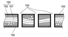
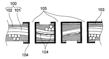
- the conventional wiring board as described above is usually manufactured as follows. That is, (1) impregnating the resin 102 into the reinforcing fiber 101 and placing the copper foil 103 on the upper and lower surfaces of the prepreg obtained by drying and curing the resin 102 by hot pressing and simultaneously bonding the copper foil 103 Thus, a so-called double-sided copper-clad substrate is produced (see FIG. 11). (2) A through-hole penetrating the copper foil 103 and the insulating substrate 100 is formed by a drill (see FIG. 12). (3) Next, a conductor layer 104 is formed on the inner surface of the formed through hole by plating to form a through hole 105 (see FIG. 13).
- the copper foil is processed into a wiring pattern-like wiring layer by a subtractive method (see FIG. 14); (5) An insulating layer called a solder resist is laminated on the main surface of the obtained substrate. Thus, a wiring board is obtained.
- Patent Documents 1 and 2 disclose prepregs in which a woven fabric of reinforcing fibers is impregnated with a curable resin, and Patent Document 3 cures to reinforcing fibers that are parallel and oriented in one direction.
- a prepreg impregnated with a conductive resin is disclosed.
- a printed wiring board usually, an insulating layer is formed on an inner layer circuit board on which an inner layer circuit is formed, a metal layer is formed thereon, a hole penetrating the entire wiring board is formed, or a via reaching the inner layer circuit is formed. A hole is formed to electrically connect the inner layer circuit and the metal foil, and unnecessary portions of the metal foil are removed by etching.
- the coefficient of thermal expansion is about 16 ppm / There was a large difference between the silicon chip and 3 ppm / ° C.
- Patent Document 1 Japanese Patent Application Laid-Open No. 2002-198658 Patent Document 2 Japanese Patent Application Laid-Open No. 2002-212394 Japanese Patent Application Laid-Open No. 10-508720 Japanese Patent Application Laid-Open No. 2005-86164
- low dielectric constant materials In recent years, with the increase in speed and functionality of LSIs, there is a tendency for low dielectric constant materials to be used on the silicon surface. Although the lowest dielectric constant material is air, there is a problem in circuit retention, so low dielectric constant material candidates tend to be materials containing many bubbles. Low dielectric constant material containing many bubbles has low strength, so when a silicon chip using such a low dielectric constant material containing bubbles is flip-chip mounted on a conventional substrate, thermal expansion between the substrate and silicon chip Due to the difference in rate, there is a problem that the low dielectric constant material on the surface of the silicon chip is cracked during the cooling process after flip chip mounting and the circuit is disconnected.
- a package for mounting a silicon chip using a low dielectric constant material containing bubbles must have a thermal expansion coefficient difference that is as small as possible and does not cause thermal stress in the silicon chip. For this reason, the thermal expansion coefficient of the package substrate is required to be as close as possible to the thermal expansion coefficient of the silicon chip.
- LSIs tend to become larger because they process a lot of data at the same time.
- I / O Input / Output
- I / O is currently on the order of thousands, but is expected to reach 10,000 in the future. For this reason, there is a tendency to reduce the size of the connection portion (bump) between the semiconductor element and the wiring board.
- bumps having a diameter of 100 ⁇ m and a pitch of 220 ⁇ m will be reduced to a diameter of 50 ⁇ m to 75 ⁇ m and a pitch of 100 ⁇ m to 125 ⁇ m. Is required.
- a package for mounting a silicon chip requiring a large bump with a large I / O must be as small as possible in the thermal expansion coefficient difference from the silicon chip so as not to cause thermal stress on the silicon chip.
- the thermal expansion coefficient of the package substrate is required to be as close as possible to the thermal expansion coefficient of the silicon chip.
- a normal insulating substrate obtained by impregnating a glass cloth with an epoxy resin has a large coefficient of thermal expansion of the glass cloth, and it has been difficult to achieve a thermal expansion coefficient equivalent to that of a silicon chip.
- a through conductor with a uniform hole diameter is required. There was a problem that it was difficult to form.
- polybenzazole fibers are produced by removing the solvent from the polymerization solution, the orientation of the microcrystals (phenylene ring and benzobisoxazole structure) aligns with the outflow of the solvent, resulting in polyparaphenylene benzobis.
- the phenylene ring plane and the benzobisoxazole structure plane in the oxazole molecule tend to be selectively oriented in the radial direction (radial).
- polyparaphenylene benzobisoxazole molecules have small intermolecular interactions.
- the problem of cracking (occurrence of cracks) is inevitable along the structure formation along the radial arrangement direction (when a cross section perpendicular to the fiber axis is formed). Even if cracks are generated in this way, the molecules are highly oriented in the fiber axis direction, so that the fiber elastic modulus and strength are not greatly affected. However, when this is used as a reinforcing material for a high-density electronic circuit board, the possibility that two through-holes cross a common crack cannot be rejected.
- the crack referred to here is a space generated inside the fiber. There is a possibility that copper atoms form a short circuit due to a migration effect in the crack and cannot serve as a circuit board (particularly for package use).
- the conductor layer 104 is formed in the through hole of the substrate and the through hole 105 is formed as shown in FIG.
- the layer 104 penetrates into the cracks in the reinforcing fiber 101. Therefore, there is a problem that the plurality of through holes 105 formed in the wiring board are likely to cause conduction breakdown through cracks in the reinforcing fiber 101.
- the present invention has been made in view of the above circumstances, and is useful for a printed wiring board excellent in long-term connection stability, a prepreg capable of forming such a substrate, and excellent in long-term connection stability.
- An object of the present invention is to provide a printed wiring board.
- polybenzazole fibers having a small number of cracks, a high elastic modulus, and a high negative linear expansion property are used as reinforcing fibers for prepreg, that is, printed wiring. It has been found that the above problems can be solved by using the substrate constituting the substrate. In addition, the present inventors have found that cracks in polybenzazole fibers can be suppressed by randomly orienting the phenylene ring plane and benzazole structure plane of the polybenzazole molecules constituting the polybenzazole fiber in the fiber diameter direction cross section. Completed the invention.
- the prepreg for a printed wiring board of the present invention that has solved the above problems is a prepreg containing polybenzazole fibers and a curable resin composition, and has a crack rate of 10 polybenzazole fibers. / 1000 m or less, an elastic modulus of 200 GPa or more and 350 GPa or less, and a linear expansion coefficient (100 ° C. or more and 200 ° C. or less) in the fiber axis direction is ⁇ 20 ppm / ° C. or more and ⁇ 3 ppm / ° C. or less.
- the printed wiring board using the substrate obtained from the prepreg for printed wiring board of the present invention is less likely to cause conduction breakdown in the formed through holes. Therefore, connection reliability is improved. Further, since the polybenzazole fiber has a high elastic modulus, the reinforcing action of the substrate is increased, and no practical problem occurs even when a thin substrate having a thickness of 0.3 mm or less is manufactured. Furthermore, since the polybenzazole fiber has a high negative linear expansion property, the linear expansion coefficient of the obtained printed wiring board can be lowered.
- the polybenzazole fiber is irradiated with X-rays in parallel with the X-axis direction with the fiber axis aligned with the Z-axis direction, and the X-ray irradiation position is scanned in the Y-axis direction.
- X-ray diffraction measurement is performed on 11 points including the center point and substantially equally spaced over the entire width of the directional fiber, and the diffraction intensity derived from the equatorial direction (200) crystal plane in the X-ray diffraction pattern obtained for each measurement position is vertically
- the polybenzazole fiber in which the line graph shows a single peak having a maximum value at or near the fiber center in the Y-axis direction has a phenylene ring plane and a benzazole structure plane that the polybenzazole molecule constituting the fiber has a preferential orientation. Therefore, cracks are hardly generated in the fibers.
- the polybenzazole fiber is a spinning step of spinning from a spinneret using a spinning stock solution containing polybenzazole and polyphosphoric acid; a temperature of 70 ° C. to 130 °
- It is preferably produced through a heat treatment step in which a tension of / dtex or more and 8.0 cN / dtex or less is applied and heat treatment is performed at 400 to 700 ° C.
- the printed wiring board prepreg of the present invention preferably has a mode in which the polybenzazole fiber is impregnated with the curable resin composition in a fiber layer oriented in a certain direction.
- the polybenzazole fiber has a multilayer structure having at least a first layer in which the polybenzazole fiber is oriented in the first direction and a second layer in which the polybenzazole fiber is oriented in a second direction different from the first direction. More preferably.
- a preferred embodiment of the prepreg for a printed wiring board according to the present invention is a woven fabric composed of the polybenzazole fiber impregnated with the curable resin composition.
- the curable resin composition used in the present invention preferably contains 20% by volume or more and 90% by volume or less of an inorganic filler and an epoxy resin, and spherical silica is suitable as the inorganic filler.
- the present invention also includes a substrate obtained from the prepreg for a printed wiring board.
- the linear expansion coefficient (100 ° C. to 200 ° C.) of the substrate is preferably ⁇ 6 ppm / ° C. to 4 ppm / ° C.
- the present invention also includes a laminate having the substrate and a metal foil laminated on at least one surface of the substrate.
- the present invention also includes a printed wiring board having a board obtained from the printed wiring board prepreg and a wiring layer provided on at least one surface of the board.
- the linear thermal expansion coefficient (100 ° C. or more and 200 ° C. or less) of the printed wiring board is preferably ⁇ 5 ppm / ° C. or more and 7 ppm / ° C. or less.
- the diffraction intensity derived from the equator direction (200) crystal plane in the X-ray diffraction pattern obtained for each measurement position is taken as the vertical axis, and the measurement position in the full width of the Y-axis direction is taken as the horizontal axis.
- the diffraction intensity derived from the equator direction (200) crystal plane in the X-ray diffraction pattern obtained for each measurement position is taken as the vertical axis, and the measurement position in the full width of the Y-axis direction is taken as the horizontal axis.
- a fiber axial direction is a right angle direction with respect to a paper surface.
- the diffraction intensity derived from the equatorial direction (200) crystal plane in the X-ray diffraction pattern obtained for each measurement position is taken as the vertical axis, and the measurement position in the full width of the Y-axis direction is taken as the horizontal axis.
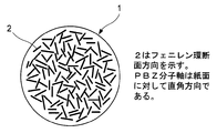
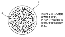
- FIG. 1 It is a schematic diagram which illustrates the fiber radial direction sectional drawing of the conventional polybenzazole fiber (The fiber axis direction is a right angle direction with respect to a paper surface). It is a schematic diagram for demonstrating the trough of a line graph. It is a schematic diagram for demonstrating the crack in a fiber, (a) is a schematic diagram which makes the fiber axis correspond to a Z-axis direction in a rectangular coordinate system, and illustrates the crack seen from the X-axis direction, (b ) Is a schematic view illustrating a crack viewed from the Y-axis direction with the fiber axis aligned with the Z-axis direction in the orthogonal coordinate system. Polybenzazole fiber no.
- Polybenzazole fiber no. 7 is a line graph of diffraction intensity with the vertical axis representing the diffraction intensity derived from the equator direction (200) crystal plane in the X-ray diffraction pattern obtained for each measurement position and the horizontal axis representing the measurement position in the full fiber width in the Y-axis direction.
- Polybenzazole fiber no. 7 is a line graph of diffraction intensity with the vertical axis representing the diffraction intensity derived from the equator direction (200) crystal plane in the X-ray diffraction pattern obtained for each measurement position and the horizontal axis representing the measurement position in the full fiber width in the Y-axis direction. .
- 8 is a line graph of diffraction intensity with the ordinate representing the diffraction intensity derived from the equator direction (200) crystal plane in the X-ray diffraction pattern obtained for each measurement position of 8 and the abscissa representing the measurement position in the full width of the fiber in the Y-axis direction.
- It is a cross-sectional schematic diagram of a double-sided copper-clad board for explaining the manufacturing process of a conventional wiring board. It is a cross-sectional schematic diagram of the double-sided copper-clad board
- the prepreg for a printed wiring board of the present invention (hereinafter sometimes simply referred to as “prepreg”) is a prepreg containing a polybenzazole fiber and a curable resin composition, and is a crack of the polybenzazole fiber.
- the modulus is 10 pieces / 1000 m or less, the elastic modulus is 200 GPa to 350 GPa, and the linear expansion coefficient in the fiber axis direction (100 ° C. to 200 ° C.) is ⁇ 20 ppm / ° C. to ⁇ 3 ppm / ° C. To do.
- the prepreg refers to a sheet-like material obtained by impregnating a curable resin into polybenzazole fibers and curing the curable resin up to the B stage.
- the B stage refers to an intermediate curing state of the thermosetting resin when, for example, a thermosetting resin is used as the curable resin composition, and the resin in this state softens when heated. Swells on contact with certain solvents, but does not melt or dissolve completely.
- the polybenzazole fiber used in the present invention is composed of a benzazole unit homopolymer, or a polybenzazole (hereinafter sometimes referred to as “PBZ”) such as a random, sequential or block copolymer polymer.
- PBZ polybenzazole
- Examples of the PBZ include “Liquid Crystalline Polymer Compositions, Process and Products”, Wolfe et al., US Pat. No. 4,703,103 (October 27, 1987); (August 6, 1985); “Liquid Crystalline Poly (2,6-Benzothiazole) Compositions, Process and Products, US Patent No. 4533724 (August 6, 1985);” Liquid Crystalline Polymers Compositions, Process and and Products ", U.S. Pat. No. 4,536,393 (August 6, 1985); Evers,” Thermooxidatively Stable “Articulated” p-Benzobisoxazole “and” p-Benzobisoxazole “Polymers", U.S. Pat. No. 4,359,567 (November 16, 1982); Examples include those described in “Method for making Heterocyclic Block Copolymer”, US Pat. No. 4578432 (March 25, 1986), and the like.
- the benzazole unit constituting the PBZ used in the polybenzazole fiber those represented by the following formulas (a) to (h) are preferable, and among these, the benzazole unit represented by (a) and (b) Polyparaphenylene benzobisoxazole (hereinafter sometimes referred to as “PBO”), and polyparaphenylene benzobisthiazole (hereinafter referred to as “PBT”) composed of benzazole units represented by (c) and (d). Is sometimes more suitable).
- PBO Polyparaphenylene benzobisoxazole
- PBT polyparaphenylene benzobisthiazole
- PBZ used for the said polybenzazole fiber what contains 80 mass% or more of PBO as a benzazole unit is preferable, and a PBO homopolymer is especially suitable.
- the polybenzazole fiber is irradiated with X-rays in parallel with the X-axis direction with the fiber axis aligned with the Z-axis direction, and the X-ray irradiation position is scanned in the Y-axis direction.
- X-ray diffraction measurement is performed on 11 points including the center point and substantially equally spaced over the entire width of the directional fiber, and the diffraction intensity derived from the equatorial direction (200) crystal plane in the X-ray diffraction pattern obtained for each measurement position is vertically
- the fiber axis is aligned with the Z-axis direction, X-rays are irradiated in parallel with the X-axis direction, the X-ray irradiation position is scanned in the Y-axis direction, and the entire fiber width in the Y-axis direction is measured.
- the X-ray diffraction measurement is performed on 11 points that are substantially equidistant including the center point, the diffraction intensity derived from the equator direction (200) crystal plane in the X-ray diffraction pattern obtained for each measurement position is taken as the vertical axis, and Y
- the line graph of the diffraction intensity shows a single peak having a maximum value at or near the Y-axis direction fiber center. Will be described.
- the measurement position of the X-ray diffraction measurement refers to the center in the Y-axis direction of the X-ray beam spot irradiated to the polybenzazole fiber.
- the (200) diffraction points were indexed according to the crystal model proposed by Fratini et al. (Material-Research-Society-Symposium-Proceedings-Vol.134-p.431 (1989)).
- the fiber center in the Y-axis direction or the vicinity thereof means that, in the diameter coordinate system, when the fiber axis is aligned with the Z-axis direction and viewed from the X-axis direction, the full fiber width in the Y-axis direction is regarded as the diameter. If the radius of the fiber is 100, the distance from the fiber center in the Y-axis direction is in the range of 0 to 50.
- the polybenzazole fiber used in the present invention irradiates X-rays in parallel with the X-axis direction with the fiber axis aligned with the Z-axis direction in the orthogonal coordinate system, and sets the X-ray irradiation position to Y.
- the total width of the Y-axis direction fiber is regarded as the diameter, and the radius of the fiber is 100.
- the position showing the maximum value of the diffraction intensity is in the range of 0 to 50 in the distance from the fiber center in the Y-axis direction.
- the position showing the maximum value of the diffraction intensity derived from the equator direction (200) crystal plane is that the distance from the fiber center in the Y-axis direction is 50, assuming that the full fiber width in the Y-axis direction is the diameter and the radius of the fiber is 100.
- the following is preferable, and more preferably 30 or less.
- a line graph of diffraction intensity with the vertical axis representing the diffraction intensity derived from the equator direction (200) crystal plane in the X-ray diffraction pattern obtained for each measurement position and the horizontal axis representing the measurement position in the full fiber width in the Y-axis direction.
- line graph of diffraction intensity shows unimodality when it is created, it means that the line graph is substantially an upwardly convex parabola.
- the waveform of the line graph only needs to show unimodality.
- Examples of the waveform of the line graph include, for example, (I) a mode in which a maximum value is shown at the fiber center in the Y-axis direction, and gradually decreases gradually toward the radially outer end (see FIG. 1); (II) The maximum value is shown at the Y-axis direction fiber center, the strength is the same as the maximum value in the vicinity of the Y-axis direction fiber center, and it gradually becomes simple as it approaches the radially outer end outside the vicinity of the Y-axis direction fiber center.
- a mode (refer FIG. 2) etc. to reduce is mentioned.
- the line graph shows unimodality, on the contrary, means that the line graph does not have valley points.
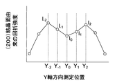
- FIG. 6 is a schematic diagram for explaining valley points in the line graph.
- the diffraction intensity (I ⁇ 1 , I 1 ) derived from the crystal plane has a large value ((I 0 ⁇ I ⁇ 1 ), (I 0 ⁇ I 1 )), and both sides 2 of the measurement position (Y 0 ) Equatorial direction (200) at the measurement position (Y -2 , Y 2 ) adjacent to the point
- the diffraction intensity (I -2 , I 2 ) derived from the crystal plane corresponds to the equator direction (Y -1 , Y 1 ) 200)
- the diffraction intensity (I -2 , I 2 ) derived from the crystal plane
- the fiber axis is aligned with the Z-axis direction, X-rays are irradiated in parallel with the X-axis direction, the X-ray irradiation position is scanned in the Y-axis direction, and the entire fiber width in the Y-axis direction is measured.
- X-ray diffraction measurement was performed on 11 points at substantially equal intervals, the diffraction intensity derived from the equator direction (200) crystal plane in the X-ray diffraction pattern obtained for each measurement position was taken as the vertical axis, and the total fiber width in the Y-axis direction.
- FIGS. 1 and 2 show the Y-axis direction fiber with the diffraction intensity derived from the equator direction (200) crystal plane in the X-ray diffraction pattern obtained for each measurement position in the polybenzazole fiber used in the present invention as the vertical axis.
- FIG. 3 is a schematic view illustrating a cross-sectional view in the fiber diameter direction of the polybenzazole fiber used in the present invention (the fiber axis direction is a direction perpendicular to the paper surface).
- FIG. 4 shows the X-ray diffraction pattern obtained for each measurement position in a conventional polybenzazole fiber with the diffraction intensity derived from the equator direction (200) crystal plane as the vertical axis and the measurement position in the full width of the Y-axis direction in the horizontal direction.
- FIG. 5 is a schematic view illustrating a cross-sectional view in the fiber radial direction of a conventional polybenzazole fiber (the fiber axis direction is a direction perpendicular to the paper surface).
- the structure plane (hereinafter, sometimes referred to as “structure plane”) is randomly oriented as shown in FIG.
- the polybenzazole fiber is As shown in FIG. 5, it is shown that the structural plane of the PBZ that is formed is selectively oriented radially outward from the center of the fiber.
- the PBZ constituting the polybenzazole fiber such as PBO has a small interaction between adjacent polymer molecules, that is, if the structural plane of the PBZ is oriented in a certain direction, the PBZ cracks along the structural plane. Is likely to occur. Therefore, as shown in FIG. 5, when the structural plane is selectively oriented radially from the center of the fiber toward the outside in the radial direction, cracks are likely to occur along the orientation direction of the structural plane.
- the structural plane is not selectively oriented in a specific direction, and is randomly oriented, so it is considered that cracks are less likely to occur. .
- the fiber axis is aligned with the Z-axis direction, X-rays are irradiated in parallel with the X-axis direction, and the X-ray irradiation position is scanned in the Y-axis direction.
- X-ray diffraction measurement method over the full width of the fiber, it is possible to measure at least about 10 points over the full width of the fiber in the Y-axis direction, that is, if the focal diameter of the X-ray used for the measurement is about 1/5 of the fiber diameter. For example, it can be measured by the method described in non-patent literature (Polymer vol. 46 (2005) p. 1935-1942).
- the crack rate of the polybenzazole fiber used in the present invention is preferably 10 pieces / 1000 m or less, more preferably 8 pieces / 1000 m or less, and further preferably 5 pieces / 1000 m or less. If the crack rate of the polybenzazole fiber is 10 pieces / 1000 m or less, the long-term connection reliability of the printed wiring board obtained using the prepreg of the present invention is further improved.
- a crack rate is the number of the cracks which exist per single fiber unit length (1000 m), and confirms with the measuring method mentioned later.
- a crack is a length in the Z-axis direction of 30 ⁇ m or more and 500 ⁇ m or less and a length in the X-axis direction of 0.5 ⁇ m or more when the fiber axis is aligned with the Z-axis direction in an orthogonal coordinate system.
- a defect having a length of 5 ⁇ m or less and a length in the Y-axis direction of 0.5 ⁇ m or more and 5 ⁇ m or less.
- the maximum length (X m , Y m , Z m ) in each direction is measured as the length in each direction of the crack.
- FIG. 7A and 7B the maximum length (X m , Y m , Z m ) in each direction is measured as the length in each direction of the crack.
- FIG. 7 is a schematic diagram for explaining cracks in the fiber
- (a) is a schematic diagram illustrating a crack viewed from the X-axis direction with the fiber axis aligned with the Z-axis direction in the orthogonal coordinate system.
- FIG. 4B is a schematic diagram illustrating a crack viewed from the Y-axis direction with the fiber axis aligned with the Z-axis direction in the orthogonal coordinate system.
- the fiber diameter of the polybenzazole fiber used in the present invention is preferably 4 ⁇ m or more, more preferably 5 ⁇ m or more, further preferably 6 ⁇ m or more, preferably 15 ⁇ m or less, more preferably 12 ⁇ m or less, still more preferably 10 ⁇ m or less. is there.
- the fiber diameter of the polybenzazole fiber is desirably smaller from the viewpoint of improving the adhesion with the resin component, but it is difficult to produce a polybenzazole fiber having a fiber diameter of less than 4 ⁇ m. There are concerns about the adverse effects on health of fibers with a small fiber diameter.
- the tensile strength of the polybenzazole fiber used in the present invention is preferably 1.8 GPa or more, more preferably 2.0 GPa or more, still more preferably 2.2 GPa or more, and preferably 7.0 GPa or less, more preferably 6 .5 GPa or less, more preferably 6.0 GPa or less.
- a thin substrate having a thickness of 0.3 mm or less is produced using the prepreg of the present invention, and even when the substrate is used in an electronic device, the substrate is cracked when the device is dropped. There is no practical problem such as.
- the elastic modulus of the polybenzazole fiber used in the present invention is preferably 200 GPa or more, more preferably 210 GPa or more, further preferably 225 GPa or more, preferably 350 GPa or less, more preferably 330 GPa or less, more preferably 300 GPa or less. is there. If the elastic modulus of the polybenzazole fiber is within the above range, even when a thin substrate having a thickness of 0.3 mm or less is produced using the prepreg of the present invention, problems such as warping and deformation of the substrate do not occur. .
- the elastic modulus of the polybenzazole fiber refers to an apparent Young's modulus defined in JIS L 1013.
- the linear thermal expansion coefficient (100 ° C. or more and 200 ° C. or less) of the polybenzazole fiber used in the present invention is preferably ⁇ 20 ppm / ° C. or more, more preferably ⁇ 15 ppm / ° C. or more, and further preferably ⁇ 10 ppm. / ° C. or more, preferably ⁇ 3 ppm / ° C. or less, more preferably ⁇ 4 ppm / ° C. or less, and still more preferably ⁇ 5 ppm / ° C. or less. If the linear thermal expansion coefficient (100 ° C. or more and 200 ° C.
- the linear thermal expansion coefficient of the printed wiring board body can be lowered.
- the polybenzazole fiber manufacturing method used in the present invention includes, for example, a spinning dope preparation process, a spinning process, a coagulation process, a washing process, a neutralization process, a drying process, and a heat treatment process.
- the spinning stock solution preparing step is a step of preparing a spinning stock solution containing the PBZ and a solvent.
- the PBZ and the spinning dope can be synthesized by a known method. For example, Wolfe et al., US Pat. No. 4,453,393 (August 6, 1985), Sybert et al., US Pat. No. 4,772,678 (September 20, 1988), Harris, US Pat. No. 4,847,350 (July 11, 1989). ).
- a polymer consisting essentially of PBO, according to Gregory et al., US Pat. No. 5,089,591 (February 18, 1992), has a high reaction rate at high reaction rates under relatively high temperature and high shear conditions in a dehydrating acid solvent. Molecular weight is possible.
- the solvent is not particularly limited as long as it contains a non-oxidizing acid solvent capable of dissolving PBZ.
- the acid solvent include polyphosphoric acid, methanesulfonic acid, high-concentration sulfuric acid, and mixtures thereof. Among these, polyphosphoric acid and methanesulfonic acid are preferable, and polyphosphoric acid is particularly preferable.
- the PBZ content in the spinning dope is preferably 7% by mass or more, more preferably 10% by mass or more, and further preferably 14% by mass or more.
- the upper limit of the PBZ content in the spinning dope is not particularly limited, but is 20% by mass in consideration of the solubility of PBZ and the viscosity of the spinning dope.
- the spinning step is a step of supplying the spinning stock solution to a spinning section of the apparatus and spinning from the spinneret.
- a known apparatus can be used for the spinning process.
- the temperature of the spinning dope when spinning from the spinneret is usually 100 ° C. or higher and 250 ° C. or lower.
- the arrangement of the pores formed in the spinneret is usually arranged in a circumferential shape or a lattice shape, but other arrangements may be used. Further, the number of pores formed in the spinneret is not particularly limited, and may be appropriately adjusted so that fusion between the spun yarns does not occur.
- the spun yarn requires a sufficiently constant draw zone as described in US Pat. No. 5,296,185 to obtain a sufficiently constant draw ratio (SDR), and a comparison It is desirable to cool uniformly with a rectified cooling air having a relatively high temperature (above the solidification temperature of the spinning dope and not more than the spinning temperature).
- the length of the draw zone needs to be a length that completes solidification in a non-solidifying gas such as nitrogen, argon, or air, and is roughly determined by the single hole discharge amount.
- the take-out stress of the draw zone needs to be 2 g / d or more in terms of polymer (assuming that only the polymer is stressed).
- solidification means that the spinning dope is cooled and simply changes from a molten state to a solid state.
- the SDR is preferably higher from the viewpoint of the linear expansion coefficient and elastic modulus of the obtained polybenzazole fiber, but if the SDR is too high, cracks are likely to occur due to fine foreign matter and viscosity spots contained in the yarn. . Therefore, for example, when obtaining a polybenzazole fiber having a fiber diameter of 4 ⁇ m or more and 15 ⁇ m or less, the pore diameter of the pores formed in the spout gold is preferably 0.10 mm or more, more preferably 0.11 mm or more, and still more preferably 0. .12 mm or more, preferably 0.17 mm or less, more preferably 0.16 mm or less, and still more preferably 0.15 mm or less.
- the coagulation step is a step of coagulating PBZ by bringing a coagulant into contact with the spun yarn.
- the spun yarn drawn in the draw zone is guided to a coagulation bath and brought into contact with a coagulant.
- the coagulant is not particularly limited as long as the acid solvent can dissolve PBZ without eluting the acid solvent used in the spinning dope from the spun yarn.
- water vapor may be used as the coagulant.
- polyphosphoric acid that can dissolve PBZ can be hydrolyzed to phosphoric acid that cannot dissolve PBZ without eluting polyphosphoric acid from the spun yarn, and thus PBZ can be coagulated.
- “solidification” means that PBZ dissolved in an acid solvent is precipitated.
- the acid solvent used in the spinning dope is not eluted from the spun yarn, and the acid solvent cannot dissolve PBZ, so that the structural plane is radial when the solvent is eluted from the spun yarn.
- Orientation radial selective orientation
- polybenzazole fibers having a structural plane randomly oriented can be obtained.
- the apparatus for spraying water vapor on the spun yarn is not particularly limited as long as the spun yarn is in contact with the water vapor and can solidify to the inside of the spun yarn. Any of a formula, a sealed type, and a non-sealed type can be used.
- the temperature of the water vapor when bringing the water vapor into contact with the spun yarn is preferably 70 ° C or higher, more preferably 80 ° C or higher, preferably 130 ° C or lower, more preferably 110 ° C or lower.
- the temperature of the water vapor is a temperature measured in the coagulation bath. If the temperature is low, the orientation pattern of the structural plane such as a phenylene ring described later cannot be sufficiently randomized. Conversely, if it is too high, the tensile strength and elastic modulus of the fiber will not reach the desired levels. Even in solidification using steam, the orientation of the structural plane is also radially oriented due to the influence of the material flow described later.
- the water vapor content in all gas components in the gas phase in the coagulation bath is preferably 80% by mass or more, more preferably 90% by mass or more, and still more preferably 95% by mass or more. If the water vapor content is low, the orientation pattern of the structure plane cannot be sufficiently randomized.
- the method / principle of randomly changing the orientation mode of the structural plane such as the phenylene ring, which is particularly important in the present invention, will be described.
- the spun yarn extruded from the spinneret encounters a coagulant, so that coagulation and structure formation (crystal growth and alignment) occur simultaneously from the surface. Over time, the place where solidification and structure formation occur moves from the surface of the spun yarn to the center.
- the polyphosphoric acid molecules that have dissolved PBZ so far will move away from the PBZ molecules, and some molecules will flow out of the spun yarn while changing to phosphoric acid due to the hydrolysis effect.
- the PBZ molecule has a planar structure (such as a phenylene ring) in the molecular structure.
- steam is used as a coagulant to increase the temperature of the fiber during coagulation, increase the molecular motion of water and acid solvent (polyphosphoric acid), and promote the hydrolysis reaction of polyphosphoric acid. is important.
- the difference in chemical potential between the spun yarn and the coagulating liquid is reduced. That is, it is important to suppress the outflow of phosphoric acid or polyphosphoric acid to the coagulation bath while passing through the coagulation bath by employing steam as the coagulant.
- water molecules reach the inside of the spun yarn in a short time, and the degree of condensation of polyphosphoric acid is lowered. Since the coagulant cannot be expected to be washed away like a liquid due to the vapor, the outflow of polyphosphoric acid to the outside of the spun yarn is suppressed.
- the spun yarn immediately after leaving the coagulation bath is filled with hydrolyzed polyphosphoric acid or phosphoric acid (monophosphoric acid) until it loses its ability to dissolve PBZ. It is assumed that there is.
- the washing step is a step in which the spun yarn that has undergone the coagulation step is guided to a washing bath, and the acid solvent in the spun yarn is washed with a washing solution to form polybenzazole fibers.
- the washing liquid is not particularly limited as long as it can elute the acid solvent.
- a material capable of dissolving phosphoric acid contained in the spun yarn that has undergone the coagulation step may be used. Etc. are used.
- the monophosphoric acid and hydrolyzed polyphosphoric acid that are washed away no longer have the ability to dissolve PBZ, that is, the interaction with the PBZ molecules is very small. For this reason, it is considered that the ability to promote the orientation of a structural plane such as a phenylene ring in the (radial) direction of mass transfer is already lost. In fact, in the polybenzazole fiber thus produced, the structural plane such as the phenylene ring of the PBZ molecule is not aligned in the radial direction.
- the neutralization step is a step of neutralizing the acid solvent remaining in the polybenzazole fiber obtained in the washing step.
- the neutralization solution used in the neutralization step is not particularly limited, and examples thereof include a sodium hydroxide aqueous solution, ammonia water, and a sodium carbonate aqueous solution. In addition, it is desirable to wash with water again after neutralization.
- the drying step is a step of adjusting the moisture content of the polybenzazole fiber.
- the drying temperature is preferably 150 ° C. or higher, more preferably 200 ° C. or higher, further preferably 220 ° C. or higher, 400 ° C. or lower, more preferably 300 ° C. or lower, still more preferably 270 ° C. or lower.
- the moisture content of the polybenzazole fiber to be subjected to the heat treatment step is preferably 3% by mass or less, more preferably 2% by mass or less, and further preferably 1% by mass or less. If the water content of the polybenzazole fiber is too high, the water may suddenly boil and evaporate when subjected to a heat treatment described later, which may cause cracks in the fiber.
- the water content of the polybenzazole fiber may be measured according to JIS L 1013.
- the heat treatment step is a step of performing a heat treatment in a state where tension is applied to the polybenzazole fiber.
- the tension applied to the fiber is preferably 1.0 cN / dtex or more, more preferably 1.5 cN / dtex or more, still more preferably 2.0 cN / dtex or more, particularly preferably 2.5 cN / dtex or more, most preferably 3 0.0 cN / dtex or more, preferably 8.0 cN / dtex or less, more preferably 7.0 cN / dtex or less, and still more preferably 6.0 cN / dtex.
- the heat treatment temperature is preferably 400 ° C. or more, more preferably 500 ° C. or more, further preferably 550 ° C. or more, preferably 700 ° C. or less, more preferably 680 ° C. or less, and further preferably 630 ° C. or less.
- the said curable resin composition is a composition which uses a non-hardened resin component as an essential component and contains a hardening
- uncured resin component examples include epoxy resin, phenol resin, cyanate resin (cyanate ester resin), bismaleimide resin, uncured triazine resin, unsaturated polyester resin, two-component curable polyurethane resin, uncured polyimide resin, Examples include uncured acrylate resins and uncured silicone resins. These resins may be used alone or in combination of two or more. As the resin, a plurality of types of mixtures are preferably used, and a mixture of an epoxy resin and a phenol resin is more preferable.
- epoxy resin glycidyl ether type obtained by reaction of phenols or alcohols with epichlorohydrin; glycidyl ester type obtained by reaction of carboxylic acids with epichlorohydrin; obtained by reaction of amines or cyanuric acid with epichlorohydrin Examples include glycidylamine type. Among these, glycidyl ether type is preferable.
- glycidyl ether type epoxy resins are further classified into bisphenol A novolak type; phenol novolak type; cresol novolak type, etc., depending on the compounds used as phenol derivatives, but bisphenol A novolak type epoxy resins are more preferred. .
- the phenol resin is classified into a novolac resin and a resol resin, and a novolac resin is preferable.
- a novolac resin is preferable.
- the novolak resins bisphenol A type novolak resins and triazine-modified novolak resins are more preferable.
- the curable resin composition may contain a curing agent as necessary. What is necessary is just to select the said hardening
- an epoxy resin is contained as the resin
- an imidazole compound such as 2-ethyl-4-methylimidazole
- a polyamine-based curing agent such as 2-ethyl-4-methylimidazole
- a polymercaptan curing agent can be used.
- the curable resin composition preferably contains an inorganic filler.
- an inorganic filler what consists of nonelectroconductive materials is preferable, For example, what consists of metal oxides, such as a silica, an alumina, a zirconia, a silicon carbide, aluminum hydroxide, is mentioned.
- metal oxides such as a silica, an alumina, a zirconia, a silicon carbide, aluminum hydroxide
- the shape of the inorganic filler include a spherical shape, a spheroid shape, a thin plate shape, and a needle shape. These inorganic fillers may be used alone or in combination of two or more. Among these, particles made of silica are preferable, and spherical silica is particularly preferable.
- the spherical silica is not particularly limited, and for example, those produced by treating a silicon compound in a flame or those produced by treating a silicon oxide powder in a flame can be used
- the size of the inorganic filler is desirably as fine as possible.
- the volume average particle diameter is preferably 7 ⁇ m or less, more preferably 4 ⁇ m or less, and even more preferably 2 ⁇ m or less.
- the average particle diameter of the inorganic filler is a value measured by a laser diffraction type particle size distribution analyzer.
- the surface of the inorganic filler is preferably subjected to silane coupling treatment.
- silane coupling process of an inorganic filler by a well-known method.
- the content of the inorganic filler in the curable resin composition is preferably 20% by volume or more, more preferably 45% by volume or more, and further preferably 60% by volume. % Or more.
- 90% by volume or less is preferable, and more preferably 85% by volume or less.
- the curable resin composition may contain an additive to the extent that the effects of the present invention are not impaired.
- the additive include a flame retardant such as a condensed phosphate ester.
- the linear thermal expansion coefficient (100 ° C. or more and 200 ° C. or less) of the cured product of the curable resin composition is preferably 40 ppm / ° C. or less, more preferably 20 ppm / ° C. or less, and further preferably 10 ppm / ° C. or less. If the linear thermal expansion coefficient (100 ° C. or higher and 200 ° C. or lower) of the cured product of the curable resin composition is within the above range, copper or the like that forms a wiring layer in a printed wiring board obtained using the prepreg of the present invention Even when the amount of the metal used is large or when the content ratio of the resin component in the substrate is high, the linear thermal expansion coefficient of the printed wiring board body can be lowered.
- the Young's modulus of the cured product of the curable resin composition is not particularly limited, but is 5 GPa or more and 50 GPa or less.
- the Young's modulus of the curable resin composition may be measured according to JIS K 7161.
- the prepreg of the present invention may contain polybenzazole fibers and a curable resin composition.
- a curable resin composition for example, (I) an embodiment in which polybenzazole fibers are dispersed in the form of fibers such as single fibers, spun yarns, chopped fibers, staple fibers in the curable resin composition; II) A mode in which a polybenzazole fiber is impregnated with a curable resin composition in a fiber layer oriented in a certain direction (see, for example, FIG.
- a polybenzazole fiber is A prepreg obtained by impregnating a curable resin composition into a fiber multilayer body in which a plurality of fiber layers oriented in a certain direction are laminated, wherein the fiber multilayer body includes at least a polybenzazole fiber in a first direction.
- the textile consists of polybenzazole fiber, embodiments comprising impregnated with the curable resin composition.
- the embodiments (II) to (IV) are preferable, and the embodiment (III) is most preferable.
- the method for producing the prepreg of the present invention is not particularly limited.
- a curable resin composition may be impregnated into a non-woven fabric, woven fabric, knitted fabric or the like made of polybenzazole fiber.
- the method for impregnating polybenzazole fiber with the curable resin composition is not particularly limited, and a known method may be employed.
- the curable resin composition is preferably diluted with a solvent.
- a solvent methyl ethyl ketone, ethylene glycol monomethyl ether, propylene glycol monomethyl ether, or the like is used.
- the solvent it is necessary to volatilize the solvent after impregnation with the curable resin composition.
- the drying method at this time is not particularly limited, and a known method may be adopted.
- the content of the curable resin composition in the prepreg is preferably 20% by volume or more, more preferably 25% by volume or more, still more preferably 30% by volume or more, and preferably 60% by volume or less, more preferably 50% by volume. % Or less, more preferably 40% by volume or less.
- the thickness of the prepreg is preferably 100 ⁇ m or less, more preferably 70 ⁇ m or less, and still more preferably 50 ⁇ m or less. If the prepreg is too thick, it is difficult to increase the mass fraction of the polybenzazole fiber contained, and the thermal expansion coefficient of the resulting substrate cannot be suppressed.
- the lower limit of the thickness of the prepreg is not particularly limited, but is about 30 ⁇ m in consideration of the performance of the processing apparatus and the fiber diameter of the polybenzazole fiber.
- the substrate obtained from the prepreg of the present invention will be described.
- the substrate is obtained by curing a curable resin composition contained in a prepreg. What is necessary is just to select the hardening method of the said curable resin composition according to the kind of the resin component and hardening
- the linear thermal expansion coefficient of the printed wiring board on which the silicon chip is mounted is within a range described later. If the linear thermal expansion coefficient of the printed wiring board is within this range, the silicon chip can be mounted without a problem with a stable yield without being affected by the size and material of the silicon chip. In order to keep the linear thermal expansion coefficient of the printed wiring board within the range described later, it is necessary to cancel the increase in the linear thermal expansion coefficient caused by forming a wiring layer (for example, copper wiring) on the board.
- a wiring layer for example, copper wiring
- the linear thermal expansion coefficient (100 ° C. or higher and 200 ° C. or lower) of the substrate obtained by curing the prepreg is preferably ⁇ 6 ppm / ° C. or higher, more preferably ⁇ 5 ppm / ° C. or higher, and 4 ppm / ° C. or lower. Preferably, it is 0 ppm / ° C. or less, more preferably ⁇ 2 ppm / ° C. or less. If the linear thermal expansion coefficient (100 ° C. or higher and 200 ° C. or lower) of the substrate is within the above range, even when various wiring layers are formed on the substrate obtained by curing the prepreg, the linear thermal expansion coefficient of the printed wiring substrate. Can be within the range described below. That is, design restrictions for keeping the thermal expansion coefficient of the printed wiring board within a predetermined range are reduced.
- the laminate is obtained by previously laminating a metal foil on one side or both sides of the prepreg and then curing the curable resin composition. Since the laminate has a metal foil laminated on the substrate, the wiring layer can be easily formed by etching the metal foil, and the production of the printed wiring board is facilitated.
- the thickness of the metal foil is preferably 1 ⁇ m or more and 18 ⁇ m or less.
- said metal foil if it has electroconductivity, it will not specifically limit, However, Copper foil is suitable.
- As an aspect of the laminated body an aspect in which copper foil is laminated on both surfaces of the substrate, a so-called double-sided copper-clad substrate is preferable.
- the prepreg of the present invention is particularly suitable as a substrate constituting a printed wiring board because it contains a small number of cracks in the contained polybenzazole fiber and has a low coefficient of linear thermal expansion.
- the printed wiring board of the present invention includes a substrate obtained from the prepreg for a printed wiring board of the present invention and a wiring layer provided on at least one surface of the substrate.
- the wiring layer may be provided only on one side of the substrate or may be provided on both sides.
- the formation method of the said wiring layer is not specifically limited, Well-known methods, such as an etching method, a plating method, a transfer method, are employable. Among these, when the metal foil is laminated in advance when the substrate is obtained from the prepreg as described above, the etching method is suitable.
- a through hole may be formed.
- the through hole is formed, for example, by forming a through-hole penetrating the substrate and the copper foil constituting the double-sided copper-clad substrate, and forming a conductive layer on the inner surface of the through-hole to make it conductive.
- the method for forming the through-hole is not particularly limited, and for example, a known method such as laser processing or drilling can be employed. Among these, laser processing is preferable.
- the diameter of the through hole is preferably 200 ⁇ m or less, more preferably 100 ⁇ m or less, and still more preferably 60 ⁇ m or less. By setting the diameter of the through hole in the above range, the density of the through holes formed in the printed wiring board can be increased, and a semiconductor having a large number of I / Os (input / output (connection terminals)) can be mounted. It becomes.
- Examples of the method for making the through hole conductive include methods such as electroplating, electroless plating, sputtering, vapor deposition, and filling of a conductive paste. Among these, electroplating or electroless plating is preferable, and it is more preferable to perform electrolytic plating after performing electroless plating.
- the printed wiring board of the present invention may be a so-called multilayer printed wiring board in which an insulating layer and a wiring layer are further formed on a wiring layer provided on the board.
- the manufacturing method of the said multilayer printed wiring board is not specifically limited, For example, what is necessary is just to employ
- the linear thermal expansion coefficient (100 ° C. or more and 200 ° C. or less) of the printed wiring board of the present invention is preferably ⁇ 5 ppm / ° C. or more, more preferably ⁇ 2 ppm / ° C. or more, further preferably 1 ppm / ° C. or more, and 7 ppm / ° C or lower is preferable, more preferably 6 ppm / ° C or lower, and further preferably 5 ppm / ° C or lower. If the linear thermal expansion coefficient (100 ° C. or more and 200 ° C.
- the linear thermal expansion coefficient of the printed wiring board is a value obtained by measuring the wiring layer provided on the board, and is measured by a method described later.
- a substrate useful for a printed wiring board having excellent long-term connection stability and a prepreg capable of forming such a substrate can be obtained.
- a printed wiring board having excellent long-term connection stability can be obtained.
- Evaluation method 1 Fiber diameter A fiber bundle of polybenzazole fibers embedded in an epoxy resin (G-2, manufactured by Gatan) was polished to obtain a cross section for observation. The cross section of the obtained fiber for observation was observed using an electrolytic emission scanning electron microscope (manufactured by Hitachi High-Technologies Corporation, “S-4500”), and the fiber diameter was measured. The observation fiber cross section was subjected to carbon deposition before observation, and the electron microscope was observed with an acceleration voltage set at 5 kV to 10 kV and a magnification set at 1000 to 3000 times. And after measuring a fiber diameter about at least 100 single fiber, these average values were calculated
- S-4500 electrolytic emission scanning electron microscope
- the linear thermal expansion coefficient of the fiber The thermal expansion of the polybenzazole fiber in the fiber axis direction was measured using a thermomechanical measurement apparatus (TMA) (manufactured by TA Instruments Inc., model number “Q400EM”). A fiber bundle composed of 166 polybenzazole fibers was used as a measurement sample, and the load was adjusted to 1 g or less per polybenzazole fiber. The temperature increase rate was set to 10 ° C./min, and the dimensional change in the fiber axis direction of the fiber occurring between the temperatures of 100 ° C. and 200 ° C. was measured. The linear thermal expansion coefficient was calculated from the following formula based on the obtained measurement results.
- TMA thermomechanical measurement apparatus
- ⁇ ⁇ L / (L ⁇ ⁇ T) ⁇ : Linear thermal expansion coefficient (ppm / ° C) ⁇ L: Dimensional change of sample (m) L: Original length of the sample (m) ⁇ T: Temperature change (° C)
- X-Ray Diffraction Measurement (200) The evaluation of the selective orientation of the crystal plane was performed using the X-ray diffraction method.
- a large synchrotron radiation facility ESRF European Synchrotron Radiation Facility, location: Grenoble, France
- ESRF European Synchrotron Radiation Facility, location: Grenoble, France
- the X-ray (0.98 mm) taken out from the storage ring was set to converge at the sample (polybenzazole fiber) position after being monochromatic.
- the size of the focal point was adjusted so that the diameter became 1 ⁇ m or less through the capillary optical system.
- the polybenzazole fiber is aligned with the Z-axis direction in the diameter coordinate system, X-rays are irradiated parallel to the X-axis direction, and the X-ray irradiation position is scanned in the Y-axis direction.
- X-ray diffraction measurement was performed on 11 points including the center point and substantially equidistant over the entire width of the fiber in the axial direction.
- X-ray diffraction patterns were recorded using a CCD camera (MARCCO detector: spatial resolution 64.45 ⁇ 64.45 ⁇ m 2 ). The recorded image data was transferred to a personal computer to cut out data in the equator direction and the azimuth direction, and then the diffraction intensity derived from the equator direction (200) crystal plane at each measurement position was evaluated.
- the diffraction intensity derived from the equator direction (200) crystal plane is taken as the vertical axis, and a line graph of diffraction intensity is created with the measurement position in the Y-axis direction full width of the fiber as the horizontal axis, The position and waveform of the maximum value of the line graph of the diffraction intensity were confirmed.
- the position of the maximum value was “possible” when the maximum value was at or near the fiber center in the Y-axis direction, and “impossible” otherwise.
- the waveform was determined to be “possible” when unimodality was indicated, and “impossible” otherwise.
- Linear thermal expansion coefficient of substrate and printed wiring board Sample for thermal expansion measurement (length 10mm, width 3mm, thickness 0.5mm) was cut out from the substrate obtained from the prepreg obtained in the production example and printed wiring board, and thermomechanical measurement Thermal expansion was measured using an apparatus (TMA). The temperature increase rate was set to 10 ° C./min, and the dimensional change that occurred between the temperatures of 100 ° C. and 200 ° C. was measured. Based on the obtained measurement results, the linear thermal expansion coefficients of the substrate and the printed wiring board were calculated in the same manner as the linear thermal expansion coefficient of the fiber.
- solder heat resistance test About the double-sided copper clad board obtained by the manufacture example, the solder heat resistance test was done according to JISC6481. Specifically, the double-sided copper-clad substrate was floated in a solder bath heated to 260 ° C. for 20 seconds, and then the presence or absence of swelling of the sample was visually observed. A sample in which discoloration due to blistering or peeling of the layer was observed was judged as defective.
- the migration test was performed using a printed wiring board that had been able to ensure insulation as a test board.
- the migration test was performed according to JEDEC A 101B. The test is performed in an atmosphere of a temperature of 85 ° C. and a relative humidity of 85%, the voltage applied to the electrode is 5 V, and the insulation is maintained for 1000 hours or more, and the insulation breakdown occurs in less than 1000 hours is rejected. did.
- Production Example 1 of Polybenzazole Fiber 1 PBO having an intrinsic viscosity of 24.2 dl / g obtained by the method shown in US Pat. No. 4,536,393 was dissolved in polyphosphoric acid to prepare a spinning dope having a PBO concentration of 14% by mass.
- the obtained spinning solution was spun from a spinneret having a pore diameter of 0.14 mm and a hole number of 166 at a spinning temperature of 175 ° C., and the spun yarn was passed through a quench chamber having a quench temperature of 60 ° C. and cooled. While converging the spun yarn that has passed through the quench chamber into multifilaments, water vapor is spouted at a water vapor temperature of 95 ° C.
- the spun yarn was solidified.
- the coagulated spun yarn was washed with water until the residual phosphorus concentration in the filament was 6000 ppm or less, neutralized with 1% NaOH aqueous solution for 5 seconds, and further washed with water for 10 seconds. After washing with water, it was dried until the moisture content reached 2% by mass. After drying, heat treatment was performed for 2.4 seconds under the conditions of a tension of 5.0 cN / dtex and a temperature of 600 ° C. 1 was obtained.
- Production Example 2 Polybenzazole was prepared in the same manner as in Production Example 1, except that the steam application conditions in the coagulation step were changed to a water vapor temperature of 65 ° C. and a water vapor fraction of 90% by mass in all gas components in the gas phase in the coagulation bath. Fiber No. 2 was prepared and evaluated. The results are shown in Table 1.
- Production Example 3 Polybenzazole was prepared in the same manner as in Production Example 1 except that the steam application conditions in the coagulation step were changed to a water vapor temperature of 135 ° C. and a water vapor fraction of 90% by mass in all gas components in the gas phase in the coagulation bath. Fiber No. 3 was made and evaluated. The results are shown in Table 1.
- Production Example 4 Polybenzazole was prepared in the same manner as in Production Example 1, except that the steam application conditions in the coagulation step were changed to a water vapor temperature of 95 ° C. and a water vapor fraction of 75% by mass in all gas components in the gas phase in the coagulation bath. Fiber No. 4 was prepared and evaluated. The results are shown in Table 1.
- Production Example 5 In the same manner as in Production Example 1, except that the spinneret in the spinning process was changed to a spinneret having a hole diameter of 0.18 mm and a hole number of 166, the polybenzazole fiber No. 5 was prepared and evaluated. The results are shown in Table 1.
- Production Example 6 In the same manner as in Production Example 1, except that the spinneret in the spinning process was changed to a spinneret having a hole diameter of 0.12 mm and a hole number of 166, the polybenzazole fiber No. 6 was produced, but thread breakage occurred frequently and it was difficult to produce fibers. Therefore, polybenzazole fiber no. For No. 6, only the fiber diameter was measured, and other physical property values were not measured.
- Production Example 7 In the coagulation step, polybenzazole fiber No. 1 was prepared in the same manner as in Production Example 1 except that water (temperature 40 ° C.) was used as the coagulant. 7 was made and evaluated. The results are shown in Table 1. Moreover, the line graph of the diffraction intensity produced based on the X-ray-diffraction measurement result was shown in FIG.
- steam provision is made to pass a spinning yarn for 0.6 second in the steam atmosphere adjusted to water vapor
- the coagulated spun yarn was washed with water until the residual phosphorus concentration in the filament was 5000 ppm or less, neutralized with 1% NaOH aqueous solution for 5 seconds, and further washed with water for 10 seconds. After washing with water, it was dried until the moisture content reached 2% by mass. After drying, heat treatment was performed for 2.4 seconds under the conditions of a tension of 5.0 cN / dtex and a temperature of 600 ° C. 10 were made and evaluated.
- Production Example 11 Polybenzazole fiber in the same manner as in Production Example 10 except that the vapor atmosphere in the coagulation step was changed to a water vapor temperature of 120 ° C. and a water vapor fraction of 90% by mass in all gas components in the gas phase in the coagulation bath. No. 11 was made and evaluated. The results are shown in Table 1.
- Polybenzazole fiber No. Nos. 1 and 8 had a crack rate of 4 pieces / 1000 m and 7 pieces / 1000 m, respectively, and the number of cracks in the fiber was small.
- polybenzazole fiber No. 1 and 8 are broken lines of diffraction intensity with the vertical axis representing the diffraction intensity derived from the equator direction (200) crystal plane in the X-ray diffraction pattern obtained for each measurement position and the horizontal axis representing the measurement position in the full fiber width in the Y-axis direction.
- the line graph of the diffraction intensity showed a single peak having a maximum value at or near the fiber center in the Y-axis direction.
- polybenzazole fiber No. 2 to 7 are broken lines of diffraction intensity with the vertical axis representing the diffraction intensity derived from the equator direction (200) crystal plane in the X-ray diffraction pattern obtained for each measurement position and the horizontal axis representing the measurement position in the full fiber width in the Y-axis direction.
- the line graph of the diffraction intensity did not have a maximum at or near the fiber center in the Y-axis direction and / or showed no unimodality.
- Polybenzazole fiber No. No. 9 was obtained by setting the tension in the heat treatment step to 0.7 cN / dtex. This polybenzazole fiber No. In No. 9, the number of cracks in the fiber was small, but the linear thermal expansion coefficient was as large as -1 ppm / ° C. Polybenzazole fiber no. Nos. 10 and 11 are those in which the spun yarn is taken up at a high SDR and water vapor is not sprayed onto the spun yarn in the coagulation process. These all had a large number of cracks in the fiber and a low elastic modulus.
- OGS sheet multifunctional organic green sheet
- Prepreg No. obtained 8 sheets of A are stacked, and a copper foil having a thickness of 8 ⁇ m is laminated on both sides thereof, heated and pressed at a pressure of 3.5 MPa and a temperature of 200 ° C. for 60 minutes, and a copper foil is laminated on both sides of a thickness of 600 ⁇ m (hereinafter referred to as “a”).
- a Sometimes referred to as “double-sided copper-clad substrate”) A was prepared and a solder float test was performed. The results are shown in Table 2.
- Production example B Polybenzazole fiber no. In place of polybenzazole fiber No. 1 2 except that prepreg No. 2 was used in the same manner as in Production Example A. B, double-sided copper-clad board No. B, printed wiring board No. B was prepared and evaluated. The results are shown in Tables 2 and 3.
- Production Example C Polybenzazole fiber no. In place of polybenzazole fiber No. 1 3 except that prepreg No. 3 was used in the same manner as in Production Example A. C, double-sided copper-clad board No. C, printed wiring board No. C was made and evaluated. The results are shown in Tables 2 and 3.
- Production Example D Polybenzazole fiber no. In place of polybenzazole fiber No. 1 4 except that prepreg No. 4 was used in the same manner as in Production Example A. D, double-sided copper-clad board No. D, printed wiring board No. D was made and evaluated. The results are shown in Tables 2 and 3.
- Production Example E Polybenzazole fiber no. In place of polybenzazole fiber No. 1 5 except that prepreg No. 5 was used in the same manner as in Production Example A. E, double-sided copper-clad board No. E, printed wiring board No. E was made and evaluated. The results are shown in Tables 2 and 3.
- Production Example F Polybenzazole fiber no. In place of polybenzazole fiber No. 1 No. 7 was used in the same manner as in Production Example A, except that prepreg no. F, double-sided copper-clad board No. F, printed wiring board No. F was prepared and evaluated. The results are shown in Tables 2 and 3.
- Production example G Polybenzazole fiber no. In place of polybenzazole fiber No. 1 Except for using No. 8, in the same manner as in Production Example A, the prepreg no. G, double-sided copper-clad board No. G, printed circuit board No. G was made and evaluated. The results are shown in Tables 2 and 3.
- Production example H Polybenzazole fiber No. 1 obtained in Production Example 1. 1 and in the same manner as in Production Example A, a prepreg No. 1 having a thickness of 130 ⁇ m and a curable resin composition content of 80% by volume was used. H was obtained. The obtained prepreg No. In the same manner as in Production Example A, double-sided copper-clad board No. H was produced. The obtained double-sided copper-clad substrate No. The thickness of H was 800 ⁇ m. The obtained double-sided copper-clad substrate No. In the same manner as in Production Example A, the printed wiring board No. H was produced. The obtained double-sided copper-clad substrate No. H, printed wiring board No. H was evaluated. The results are shown in Tables 2 and 3.
- Production Example I Polybenzazole fiber No. 1 obtained in Production Example 1. 1 was arranged so as to be oriented in a certain direction to form a fiber layer. The fiber layer was impregnated with the same resin varnish as in Production Example A, then dried in a dryer at 180 ° C. for 6 minutes, and the prepreg No. having a thickness of 50 ⁇ m and a curable resin composition content of 50% by volume was obtained. I was obtained. The number of fibers per unit length (perpendicular to the fibers) was 200 / mm.
- the prepreg No. I is arranged so that the fiber directions in the second and seventh prepregs are perpendicular to the fiber directions in the first and eighth prepregs from the bottom, and the second and seventh sheets
- the third and sixth prepregs are arranged so that the fiber directions in the third and sixth prepregs are orthogonal to the fiber direction in the prepreg, and the fourth and fifth fibers in the third and sixth prepregs.
- the first prepreg was placed so that the fiber directions were orthogonal to each other.
- the fiber direction in the fourth prepreg and the fiber direction in the fifth prepreg are the same.
- the obtained double-sided copper-clad substrate No. The thickness of I was 320 ⁇ m.
- the obtained double-sided copper-clad substrate No. I was used in the same manner as in Production Example A, and printed circuit board No. I was produced.
- the obtained double-sided copper-clad substrate No. I, printed wiring board No. I was evaluated. The results are shown in Tables 2 and 3.
- Production Example J Polybenzazole fiber no. In place of polybenzazole fiber No. 1 Except that 7 was used, in the same manner as in Production Example I, the prepreg no. J, double-sided copper-clad board No. J, printed circuit board No. J was prepared and evaluated. The results are shown in Tables 2 and 3.
- Production Example K As the curable resin composition, a “multifunctional organic green sheet (OGS sheet)” manufactured by Matsushita Electric Works Co., Ltd. is used, and this curable resin composition is dissolved and dispersed in an organic solvent (methyl ethyl ketone). Produced. Polybenzazole fiber No. 1 obtained in Production Example 1. 1 was arranged so as to be oriented in a certain direction to form a fiber layer. The fiber layer was impregnated with the resin varnish obtained above and then dried in a dryer at 95 ° C. for 15 minutes to obtain a prepreg No. having a thickness of 70 ⁇ m and a curable resin composition content of 60% by volume. K was obtained. The number of fibers per unit length (perpendicular to the fibers) was 210 / mm.
- OGS sheet multifunctional organic green sheet
- Prepreg No. obtained Four sheets of K were stacked, and a copper foil having a thickness of 12 ⁇ m was laminated on both sides, and heated and pressurized at a pressure of 3.5 MPa and a temperature of 180 ° C. for 60 minutes. K was obtained.
- the prepreg No. K was overlapped so that the fiber directions in the second and third prepregs were perpendicular to the fiber directions in the first and fourth prepregs from the bottom.
- the fiber direction in the second prepreg and the fiber direction in the third prepreg are the same.
- the thickness of K was 0.2 mm, and the content of the curable resin composition was 50% by volume.
- the obtained double-sided copper-clad substrate No. K in the same manner as in Production Example A, the printed circuit board No. K was produced.
- the obtained double-sided copper-clad substrate No. K, printed wiring board No. K was evaluated. The results are shown in Tables 2 and 3.
- Production Example L Polybenzazole fiber no. In place of polybenzazole fiber No. 1 7 was used in the same manner as in Production Example K except that prepreg No. 7 was used. L, double-sided copper-clad board No. L, printed wiring board No. L was made and evaluated. The results are shown in Tables 2 and 3.
- Production Example M In the same manner as in Production Example K, the prepreg No. After preparing M, the obtained prepreg No. 8 sheets of M were stacked, and a copper foil having a thickness of 12 ⁇ m was stacked on both sides, and heated and pressurized at a pressure of 3.5 MPa and a temperature of 180 ° C. for 60 minutes. M was obtained.
- the obtained double-sided copper-clad substrate No. The thickness of M was 0.4 mm.
- Production Example N Polybenzazole fiber no. In place of polybenzazole fiber No. 1 Except that 7 was used, in the same manner as in Production Example M, the prepreg no. N, double-sided copper-clad board No. N, printed wiring board No. N was made and evaluated. The results are shown in Tables 2 and 3.
- Production Example O Polybenzazole fiber no. In place of polybenzazole fiber No. 1 No. 9 was used in the same manner as in Production Example A, except that prepreg No. 9 was used. O, double-sided copper-clad board No. O, printed wiring board No. O was prepared and evaluated. The results are shown in Tables 2 and 3.
- Production Example P Polybenzazole fiber no. In place of polybenzazole fiber No. 1 10 except that prepreg No. 10 was used in the same manner as in Production Example A. P, double-sided copper-clad board No. P, printed wiring board No. P was made and evaluated. The results are shown in Tables 2 and 3.
- Production example Q Polybenzazole fiber no. In place of polybenzazole fiber No. 1 11 except that prepreg No. 11 was used in the same manner as in Production Example A.
- Q double-sided copper-clad board No. Q, printed wiring board No. Q was made and evaluated. The results are shown in Tables 2 and 3.
- the printed wiring boards of Production Examples A, G, H, I, K, M, and O are polybenzazole fiber No. What was obtained using the prepreg containing 1, 8, or 9, that is, the polybenzazole fiber contained in the substrate was polybenzazole fiber no. 1, 8 or 9. It can be seen that these printed wiring boards have excellent connection reliability since the time until conduction breakdown in the migration test is 1000 hours or more. However, the printed wiring boards of Production Examples H and O have large linear thermal expansion coefficients (100 ° C. to 200 ° C.) of 10 ppm / ° C. and 8 ppm / ° C., so that cracks occurred on the silicon chip surface in the flip chip mounting test. .
- the printed wiring boards of Production Examples B to F, J, L, N, P, and Q are polybenzazole fiber Nos. What was obtained using the prepreg containing any one of 2 to 7, 10, and 11, that is, the polybenzazole fiber contained in the substrate was polybenzazole fiber No. Any one of 2 to 7, 10, and 11. These printed wiring boards all had a time until conduction breakdown in the migration test of less than 1000 hours.
- the present invention is useful for a printed wiring board having excellent long-term connection reliability.
Landscapes
- Chemical & Material Sciences (AREA)
- Engineering & Computer Science (AREA)
- Materials Engineering (AREA)
- Manufacturing & Machinery (AREA)
- Health & Medical Sciences (AREA)
- Chemical Kinetics & Catalysis (AREA)
- Medicinal Chemistry (AREA)
- Polymers & Plastics (AREA)
- Organic Chemistry (AREA)
- Microelectronics & Electronic Packaging (AREA)
- Reinforced Plastic Materials (AREA)
- Compositions Of Macromolecular Compounds (AREA)
Abstract
Priority Applications (2)
| Application Number | Priority Date | Filing Date | Title |
|---|---|---|---|
| CN2009801212122A CN102056970A (zh) | 2008-06-30 | 2009-06-22 | 印刷配线基板用预浸料以及印刷配线基板 |
| JP2010518997A JPWO2010001754A1 (ja) | 2008-06-30 | 2009-06-22 | プリント配線基板用プリプレグおよびプリント配線基板 |
Applications Claiming Priority (4)
| Application Number | Priority Date | Filing Date | Title |
|---|---|---|---|
| JP2008-171175 | 2008-06-30 | ||
| JP2008171174 | 2008-06-30 | ||
| JP2008-171174 | 2008-06-30 | ||
| JP2008171175 | 2008-06-30 |
Publications (1)
| Publication Number | Publication Date |
|---|---|
| WO2010001754A1 true WO2010001754A1 (fr) | 2010-01-07 |
Family
ID=41465854
Family Applications (1)
| Application Number | Title | Priority Date | Filing Date |
|---|---|---|---|
| PCT/JP2009/061321 Ceased WO2010001754A1 (fr) | 2008-06-30 | 2009-06-22 | Préimprégné pour carte imprimée et carte imprimée |
Country Status (3)
| Country | Link |
|---|---|
| JP (1) | JPWO2010001754A1 (fr) |
| CN (1) | CN102056970A (fr) |
| WO (1) | WO2010001754A1 (fr) |
Cited By (2)
| Publication number | Priority date | Publication date | Assignee | Title |
|---|---|---|---|---|
| JP2016089169A (ja) * | 2014-10-30 | 2016-05-23 | Dic株式会社 | 複合樹脂組成物、成形体、熱伝導材料及び熱伝導材料 |
| US9520945B2 (en) | 2014-10-21 | 2016-12-13 | At&T Intellectual Property I, L.P. | Apparatus for providing communication services and methods thereof |
Families Citing this family (2)
| Publication number | Priority date | Publication date | Assignee | Title |
|---|---|---|---|---|
| CN104674594A (zh) * | 2015-01-14 | 2015-06-03 | 深圳昊天龙邦复合材料有限公司 | 具有负热膨胀系数和高耐热的电路板用合成纤维纸及其制备方法与应用 |
| WO2016125822A1 (fr) * | 2015-02-06 | 2016-08-11 | 東洋紡株式会社 | Élément de conversion photoélectrique, et composé semi-conducteur organique utilisé dans celui-ci |
Citations (3)
| Publication number | Priority date | Publication date | Assignee | Title |
|---|---|---|---|---|
| JPH0860437A (ja) * | 1994-08-18 | 1996-03-05 | Toyobo Co Ltd | ポリベンザゾール繊維の製造方法 |
| JPH08510791A (ja) * | 1992-08-13 | 1996-11-12 | ザ ダウ ケミカル カンパニー | ポリベンズオキサゾール繊維の紡糸後仕上げの向上した方法 |
| JP2006348442A (ja) * | 2005-06-20 | 2006-12-28 | Toyobo Co Ltd | ポリベンザゾール繊維及びその製造方法 |
-
2009
- 2009-06-22 CN CN2009801212122A patent/CN102056970A/zh active Pending
- 2009-06-22 WO PCT/JP2009/061321 patent/WO2010001754A1/fr not_active Ceased
- 2009-06-22 JP JP2010518997A patent/JPWO2010001754A1/ja active Pending
Patent Citations (3)
| Publication number | Priority date | Publication date | Assignee | Title |
|---|---|---|---|---|
| JPH08510791A (ja) * | 1992-08-13 | 1996-11-12 | ザ ダウ ケミカル カンパニー | ポリベンズオキサゾール繊維の紡糸後仕上げの向上した方法 |
| JPH0860437A (ja) * | 1994-08-18 | 1996-03-05 | Toyobo Co Ltd | ポリベンザゾール繊維の製造方法 |
| JP2006348442A (ja) * | 2005-06-20 | 2006-12-28 | Toyobo Co Ltd | ポリベンザゾール繊維及びその製造方法 |
Cited By (2)
| Publication number | Priority date | Publication date | Assignee | Title |
|---|---|---|---|---|
| US9520945B2 (en) | 2014-10-21 | 2016-12-13 | At&T Intellectual Property I, L.P. | Apparatus for providing communication services and methods thereof |
| JP2016089169A (ja) * | 2014-10-30 | 2016-05-23 | Dic株式会社 | 複合樹脂組成物、成形体、熱伝導材料及び熱伝導材料 |
Also Published As
| Publication number | Publication date |
|---|---|
| CN102056970A (zh) | 2011-05-11 |
| JPWO2010001754A1 (ja) | 2011-12-15 |
Similar Documents
| Publication | Publication Date | Title |
|---|---|---|
| US10920008B2 (en) | Thermal-curable resin composition, and pre-preg, metal-clad laminate and printed circuit board manufactured using the same | |
| KR101464008B1 (ko) | 반도체 패키지, 코어층 재료, 빌드업층 재료 및 시일링 수지 조성물 | |
| CN101605653B (zh) | 层叠体、包含该层叠体的电路板、半导体封装件及制造层叠体的方法 | |
| TWI433773B (zh) | 積層板,電路板及半導體裝置 | |
| KR101993489B1 (ko) | 프리프레그, 적층판, 다층 프린트 배선판, 및 반도체 장치 | |
| KR20140028973A (ko) | 프리프레그, 동박적층판, 및 인쇄회로기판 | |
| JP6861377B2 (ja) | プリプレグ、金属張積層板及びプリント配線板 | |
| KR101409048B1 (ko) | 회로 기판의 제조 방법, 반도체 제조 장치, 회로 기판 및 반도체 장치 | |
| JPWO2010001754A1 (ja) | プリント配線基板用プリプレグおよびプリント配線基板 | |
| JP5696786B2 (ja) | プリプレグ、積層板、半導体パッケージおよび積層板の製造方法 | |
| JP6428638B2 (ja) | 金属張積層板、回路基板、および電子装置 | |
| JP5230059B2 (ja) | プリプレグ、回路基板および半導体装置 | |
| JP7434855B2 (ja) | プリプレグ、プリント配線基板および半導体装置 | |
| JP2010031445A (ja) | ポリベンザゾール繊維 | |
| JP2009067852A (ja) | ガラス繊維織布入り絶縁樹脂シート、積層板、多層プリント配線板、及び半導体装置 | |
| CN111448043B (zh) | 预浸渍体、层叠板和它们的制造方法、以及印刷线路板和半导体封装体 | |
| JP5835401B2 (ja) | プリプレグ、回路基板および半導体装置 | |
| US20260107820A1 (en) | Manufacture method for a packaging substrate | |
| JP2011179001A (ja) | プリプレグ、回路基板および半導体装置 | |
| JP2023150255A (ja) | プリプレグ、金属張積層板、プリント配線基板および半導体装置 | |
| JP4885591B2 (ja) | 配線基板用織布およびプリプレグ | |
| JP2008101062A (ja) | 樹脂組成物、プリプレグ、積層板、及び半導体装置 | |
| JP2008251891A (ja) | 回路基板及びその半導体装置 | |
| JP2002076619A (ja) | プリント配線板製造用積層体 | |
| JP2011049323A (ja) | 電子回路用積層板 |
Legal Events
| Date | Code | Title | Description |
|---|---|---|---|
| WWE | Wipo information: entry into national phase |
Ref document number: 200980121212.2 Country of ref document: CN |
|
| 121 | Ep: the epo has been informed by wipo that ep was designated in this application |
Ref document number: 09773332 Country of ref document: EP Kind code of ref document: A1 |
|
| WWE | Wipo information: entry into national phase |
Ref document number: 2010518997 Country of ref document: JP |
|
| NENP | Non-entry into the national phase |
Ref country code: DE |
|
| 122 | Ep: pct application non-entry in european phase |
Ref document number: 09773332 Country of ref document: EP Kind code of ref document: A1 |