WO2010004875A1 - Substrat flexible et structure de circuit électrique - Google Patents
Substrat flexible et structure de circuit électrique Download PDFInfo
- Publication number
- WO2010004875A1 WO2010004875A1 PCT/JP2009/061505 JP2009061505W WO2010004875A1 WO 2010004875 A1 WO2010004875 A1 WO 2010004875A1 JP 2009061505 W JP2009061505 W JP 2009061505W WO 2010004875 A1 WO2010004875 A1 WO 2010004875A1
- Authority
- WO
- WIPO (PCT)
- Prior art keywords
- wiring pattern
- flexible substrate
- electric circuit
- substrate
- flexible
- Prior art date
- Legal status (The legal status is an assumption and is not a legal conclusion. Google has not performed a legal analysis and makes no representation as to the accuracy of the status listed.)
- Ceased
Links
Images



Classifications
-
- H—ELECTRICITY
- H05—ELECTRIC TECHNIQUES NOT OTHERWISE PROVIDED FOR
- H05K—PRINTED CIRCUITS; CASINGS OR CONSTRUCTIONAL DETAILS OF ELECTRIC APPARATUS; MANUFACTURE OF ASSEMBLAGES OF ELECTRICAL COMPONENTS
- H05K3/00—Apparatus or processes for manufacturing printed circuits
- H05K3/0011—Working of insulating substrates or insulating layers
- H05K3/0044—Mechanical working of the substrate, e.g. drilling or punching
- H05K3/0052—Depaneling, i.e. dividing a panel into circuit boards; Working of the edges of circuit boards
-
- G—PHYSICS
- G02—OPTICS
- G02F—OPTICAL DEVICES OR ARRANGEMENTS FOR THE CONTROL OF LIGHT BY MODIFICATION OF THE OPTICAL PROPERTIES OF THE MEDIA OF THE ELEMENTS INVOLVED THEREIN; NON-LINEAR OPTICS; FREQUENCY-CHANGING OF LIGHT; OPTICAL LOGIC ELEMENTS; OPTICAL ANALOGUE/DIGITAL CONVERTERS
- G02F1/00—Devices or arrangements for the control of the intensity, colour, phase, polarisation or direction of light arriving from an independent light source, e.g. switching, gating or modulating; Non-linear optics
- G02F1/01—Devices or arrangements for the control of the intensity, colour, phase, polarisation or direction of light arriving from an independent light source, e.g. switching, gating or modulating; Non-linear optics for the control of the intensity, phase, polarisation or colour
- G02F1/13—Devices or arrangements for the control of the intensity, colour, phase, polarisation or direction of light arriving from an independent light source, e.g. switching, gating or modulating; Non-linear optics for the control of the intensity, phase, polarisation or colour based on liquid crystals, e.g. single liquid crystal display cells
- G02F1/133—Constructional arrangements; Operation of liquid crystal cells; Circuit arrangements
- G02F1/1333—Constructional arrangements; Manufacturing methods
- G02F1/1345—Conductors connecting electrodes to cell terminals
- G02F1/13452—Conductors connecting driver circuitry and terminals of panels
-
- H—ELECTRICITY
- H05—ELECTRIC TECHNIQUES NOT OTHERWISE PROVIDED FOR
- H05K—PRINTED CIRCUITS; CASINGS OR CONSTRUCTIONAL DETAILS OF ELECTRIC APPARATUS; MANUFACTURE OF ASSEMBLAGES OF ELECTRICAL COMPONENTS
- H05K1/00—Printed circuits
- H05K1/02—Details
- H05K1/0266—Marks, test patterns or identification means
- H05K1/0268—Marks, test patterns or identification means for electrical inspection or testing
-
- H—ELECTRICITY
- H05—ELECTRIC TECHNIQUES NOT OTHERWISE PROVIDED FOR
- H05K—PRINTED CIRCUITS; CASINGS OR CONSTRUCTIONAL DETAILS OF ELECTRIC APPARATUS; MANUFACTURE OF ASSEMBLAGES OF ELECTRICAL COMPONENTS
- H05K1/00—Printed circuits
- H05K1/02—Details
- H05K1/11—Printed elements for providing electric connections to or between printed circuits
- H05K1/118—Printed elements for providing electric connections to or between printed circuits specially for flexible printed circuits, e.g. using folded portions
-
- H—ELECTRICITY
- H05—ELECTRIC TECHNIQUES NOT OTHERWISE PROVIDED FOR
- H05K—PRINTED CIRCUITS; CASINGS OR CONSTRUCTIONAL DETAILS OF ELECTRIC APPARATUS; MANUFACTURE OF ASSEMBLAGES OF ELECTRICAL COMPONENTS
- H05K2201/00—Indexing scheme relating to printed circuits covered by H05K1/00
- H05K2201/03—Conductive materials
- H05K2201/0332—Structure of the conductor
- H05K2201/0388—Other aspects of conductors
- H05K2201/0394—Conductor crossing over a hole in the substrate or a gap between two separate substrate parts
-
- H—ELECTRICITY
- H05—ELECTRIC TECHNIQUES NOT OTHERWISE PROVIDED FOR
- H05K—PRINTED CIRCUITS; CASINGS OR CONSTRUCTIONAL DETAILS OF ELECTRIC APPARATUS; MANUFACTURE OF ASSEMBLAGES OF ELECTRICAL COMPONENTS
- H05K2201/00—Indexing scheme relating to printed circuits covered by H05K1/00
- H05K2201/09—Shape and layout
- H05K2201/09209—Shape and layout details of conductors
- H05K2201/09654—Shape and layout details of conductors covering at least two types of conductors provided for in H05K2201/09218 - H05K2201/095
- H05K2201/09727—Varying width along a single conductor; Conductors or pads having different widths
-
- H—ELECTRICITY
- H05—ELECTRIC TECHNIQUES NOT OTHERWISE PROVIDED FOR
- H05K—PRINTED CIRCUITS; CASINGS OR CONSTRUCTIONAL DETAILS OF ELECTRIC APPARATUS; MANUFACTURE OF ASSEMBLAGES OF ELECTRICAL COMPONENTS
- H05K2201/00—Indexing scheme relating to printed circuits covered by H05K1/00
- H05K2201/10—Details of components or other objects attached to or integrated in a printed circuit board
- H05K2201/10613—Details of electrical connections of non-printed components, e.g. special leads
- H05K2201/10621—Components characterised by their electrical contacts
- H05K2201/10681—Tape Carrier Package [TCP]; Flexible sheet connector
-
- H—ELECTRICITY
- H05—ELECTRIC TECHNIQUES NOT OTHERWISE PROVIDED FOR
- H05K—PRINTED CIRCUITS; CASINGS OR CONSTRUCTIONAL DETAILS OF ELECTRIC APPARATUS; MANUFACTURE OF ASSEMBLAGES OF ELECTRICAL COMPONENTS
- H05K2203/00—Indexing scheme relating to apparatus or processes for manufacturing printed circuits covered by H05K3/00
- H05K2203/15—Position of the PCB during processing
- H05K2203/1545—Continuous processing, i.e. involving rolls moving a band-like or solid carrier along a continuous production path
-
- H—ELECTRICITY
- H05—ELECTRIC TECHNIQUES NOT OTHERWISE PROVIDED FOR
- H05K—PRINTED CIRCUITS; CASINGS OR CONSTRUCTIONAL DETAILS OF ELECTRIC APPARATUS; MANUFACTURE OF ASSEMBLAGES OF ELECTRICAL COMPONENTS
- H05K2203/00—Indexing scheme relating to apparatus or processes for manufacturing printed circuits covered by H05K3/00
- H05K2203/17—Post-manufacturing processes
- H05K2203/175—Configurations of connections suitable for easy deletion, e.g. modifiable circuits or temporary conductors for electroplating; Processes for deleting connections
Definitions
- the present invention relates to a flexible substrate that is punched in a state in which a wiring pattern is formed on a base film and is individually separated, and an electric circuit structure having the flexible substrate and an electric circuit substrate to which the flexible substrate is connected,
- the present invention relates to a flexible substrate and an electric circuit structure that do not cause short-circuit defects caused by wiring pattern chips generated when the flexible substrate is punched.
- a panel substrate constituting a flat panel image display element such as a liquid crystal panel has a pixel electrode constituting one unit of image display on its inner surface, a switching element for applying a predetermined charge to the pixel electrode, metal wiring, etc.
- This is an electric circuit board on which various electric circuit elements are formed.
- an electrode terminal drawn from a metal wiring formed in an image display area where an image is displayed is provided, and a flexible substrate (FPC: Flexible-Printed-Circuits) is provided on the electrode terminal.
- FPC Flexible-Printed-Circuits
- various signals for image display, power supply voltage for operating the panel substrate as an electric circuit substrate, and the like are supplied from a peripheral circuit substrate other than the liquid crystal panel.
- the peripheral circuit substrate is fixed to the back surface of a bottomed frame-shaped mechanism member called a bezel that accommodates a liquid crystal panel or a backlight, and a liquid crystal display as an electric circuit structure
- the device is configured.
- the flexible substrate used for connecting the panel substrate and the peripheral circuit substrate has a predetermined wiring pattern made of a metal foil such as copper foil formed on a flexible base film, and further insulates the surface thereof. It is covered with a sex protective layer.
- the connection portion of the flexible substrate with the panel substrate is provided with an opening in the base film to expose the wiring pattern, and the wiring pattern is in direct contact with the electrode terminal on the panel substrate, so that electrical contact can be obtained.
- the liquid crystal display device also employs a TCP (Tape Carrier Package) in which circuit elements such as a driving semiconductor chip and a capacitor connected to a wiring pattern are mounted on a flexible substrate.
- TCP Transmission Carrier Package
- these flexible substrates are formed continuously in a tape body with a circuit element such as a semiconductor chip mounted thereon. At the time of connection, the tape body is punched into a predetermined shape by a mold and separated individually.
- Patent Document 1 in order to prevent a wiring pattern from being peeled off from a base film and becoming a conductive foreign material due to stress caused by a punching die when a flexible substrate is punched, a short circuit failure between adjacent wiring patterns occurs.
- a technique for providing a wiring pattern having a length that does not reach the punching line at the end of the flexible substrate by alternately changing the length of the wiring pattern is disclosed.
- the chip of the wiring pattern generated when the flexible substrate is punched can be prevented from being short-circuited due to adhering to the end of the flexible substrate. It is impossible to prevent the occurrence of a short circuit defect caused by adhering to another electric circuit substrate connected to a flexible substrate such as a panel substrate.
- the width of the electrode terminals formed on the panel substrate is designed to be as wide as possible, so that the wiring pattern on the flexible substrate formed at the same pitch is more than The interval is narrow. For this reason, since it is inevitable that chips of the wiring pattern are generated when the flexible substrate is punched, it is necessary to sufficiently cope with short-circuit defects on the panel substrate.
- the present invention reduces a short circuit failure caused by wiring pattern chips generated when a flexible substrate is punched, and an electric circuit connected to the flexible substrate.
- An object is to provide an electric circuit structure having a substrate.
- the flexible substrate of the present invention is a flexible substrate in which a wiring pattern is formed on a flexible base film, and the flexible substrate has a wiring pattern formed on the base film.
- the wiring pattern is individually separated by being punched in a state where the wiring film is formed, and the wiring pattern has a narrow portion whose width is narrowed at an end portion of the base film.
- the electric circuit structure of the present invention includes the flexible substrate according to the present invention, and an electric circuit substrate on the surface of which an electric circuit element and electrode terminals connected to the electric circuit element are formed.
- the wiring pattern of the board is connected to the electrode terminal of the electric circuit board.
- the flexible board which prevents the short circuit failure caused by the wiring pattern chips, and the flexible board And an electric circuit structure having an electric circuit board to which the electric circuit board is connected.
- FIG. 1 is a plan view showing a configuration of a flexible substrate according to an embodiment of the present invention.
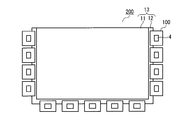
- FIG. 2 is a diagram showing a schematic configuration of the liquid crystal display device according to the embodiment of the present invention.
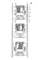
- FIG. 3 is a plan view showing the configuration of the tape body on which the flexible substrate according to the embodiment of the present invention is formed.
- FIG. 4 is a partially enlarged view showing a state before the flexible substrate according to the embodiment of the present invention is punched from the tape body.
- FIG. 5 is a diagram showing the relationship between the wiring pattern of the flexible board according to the embodiment of the present invention and the electrode terminals on the electric circuit board to which the flexible board is connected.
- the flexible substrate according to the present invention is a flexible substrate in which a wiring pattern is formed on a flexible base film, and the flexible substrate is individually punched in a state in which the wiring pattern is formed on the base film. And the wiring pattern has a narrow portion whose width is narrowed at the end of the base film.
- the width of the wiring pattern in the narrow portion is the longest.
- the length of the chips can be shortened as compared with the case where it is not provided. For this reason, even if a flexible substrate is used in a state where chips of a wiring pattern are attached to the flexible substrate, it is possible to effectively prevent occurrence of a short circuit failure caused by the chips.
- the width of the narrow portion is an electrode terminal formed on another electric circuit substrate to which the flexible substrate is connected, and the wiring pattern on the end side having the narrow portion Is preferably narrower than the interval between the electrode terminals connected to each other.
- a circuit element connected to the wiring pattern is mounted. By doing in this way, a flexible substrate can be used as TCP.
- An electric circuit structure according to the present invention includes the flexible substrate according to the present invention, and an electric circuit board on the surface of which an electric circuit element and an electrode terminal connected to the electric circuit element are formed, The wiring pattern of the flexible board is connected to the electrode terminal of the electric circuit board.
- This configuration realizes an electric circuit structure that reduces the occurrence of short-circuit defects caused by chipping of the wiring pattern that occurs when the flexible substrate is punched with the wiring pattern formed on the base film. it can.
- the electric circuit structure is a liquid crystal display device
- the electric circuit substrate is a panel substrate that constitutes a liquid crystal panel and a counter substrate fixed at a predetermined interval across a liquid crystal layer.
- the electric circuit board to which the flexible board of the present invention is connected is not limited to the panel board of a liquid crystal panel, but is used for a wide range of applications such as a panel board of an image display device, an acoustic device and an information processing device. Can be connected to.
- the electric circuit structure of the present invention is not limited to a liquid crystal display device, and can be widely applied to various flat panel display devices such as organic or inorganic EL displays and field emission cold cathode display devices.
- the present invention is not limited to the display device, and can be applied to various modules in which a flexible substrate is connected to an electric circuit substrate such as a driving circuit of an audio device or an information processing device.
- each figure referred below demonstrates only the main member required in order to demonstrate this invention among the structural members of embodiment of this invention, for simplification, and was shown. Therefore, the display apparatus according to the present invention can include arbitrary constituent members that are not shown in each of the referenced drawings. Moreover, the dimension of the member in each figure does not necessarily faithfully represent the dimension of the actual component member, the dimension ratio of each member, and the like.
- FIG. 1 is a plan view showing a configuration of a flexible substrate 100 according to an embodiment of the present invention.
- the flexible substrate 100 of the present invention has a thickness on the surface of a flexible base film 1 having an insulating property such as polyimide having a thickness of about 10 to 50 ⁇ m via an adhesive layer (not shown).
- a predetermined wiring pattern 2 (2a, 2b, 2c) is formed by bonding a metal foil such as a copper foil of about 10 to 50 ⁇ m.
- the wiring pattern 2 is covered with an insulating protective film or protective sheet (not shown), and the flexible substrate 100 has a three-layer structure in which the wiring pattern 2 is sandwiched between the base film 1 and the protective film or protective sheet. ing.
- the flexible substrate 100 of this embodiment is a TCP substrate on which a semiconductor chip 4 that outputs a drive signal for driving a liquid crystal panel is mounted as a circuit element in the center of the substrate.
- the terminal portion 3 formed on the back surface of the semiconductor chip 4, that is, the side facing the wiring pattern 2 of the semiconductor chip 4 is connected through an opening (not shown) provided in the protective sheet to be covered.
- the wiring pattern 2 includes an output-side wiring pattern 2 a connected to the output terminal of the semiconductor chip 4 and an input-side wiring pattern 2 b connected to the input terminal of the semiconductor chip 4.
- the wiring pattern 2a is drawn to the upper end portion of the flexible substrate 100 in FIG. 1, and the input side wiring pattern 2b is drawn to the lower end portion of the flexible substrate 100 in FIG.
- the end portion of the flexible substrate 100 and the vicinity thereof in the output side wiring pattern 2a are narrow portions 2c where the width of the wiring is narrowed.
- the portion where the output side wiring pattern 2a is formed and the portion where the input side wiring pattern 2b is formed are provided with openings 5a, 5b is formed.
- the output-side wiring pattern 2a and the input-side wiring pattern 2b are exposed on the back side in FIG. 1 in the openings 5a and 5b, and this exposed portion is connected to each wiring pattern 2a on the flexible substrate 100, It becomes a connection part of 2b and the electrode terminal formed in the other electric circuit board
- a film material containing conductive particles called ACF (Anisotropic Conductive ⁇ Film) is attached to the opening 5a, and the output side Physical and electrical connection between each wiring of the wiring pattern 2a and a corresponding electrode terminal formed on the panel substrate 12 of the liquid crystal panel 13 is performed.
- the ACF is attached to the opening 5b, and the drive voltage of the driving semiconductor chip 4 and the input signal are generated.
- the physical and electrical contact with the corresponding electrode terminal of the external circuit board (not shown) is generated. A connection is made.
- FIG. 2 is a diagram showing a schematic configuration of a liquid crystal display device 200 described as an example of the electric circuit structure of the present invention.
- the liquid crystal display device 200 of the present embodiment includes a liquid crystal panel in which a glass counter substrate 11 and a glass panel substrate 12 on which electric circuit elements are formed sandwich a liquid crystal layer (not shown). 13 is formed.
- a color filter is formed corresponding to each pixel for displaying a color image, and a counter electrode for applying a predetermined voltage to the liquid crystal layer is formed.
- a plurality of rows and a plurality of columns are formed and pixel electrodes are arranged in a matrix, and by adjusting the potential between the pixel electrode and the counter electrode, Image display is performed by changing the alignment state of the liquid crystal layer. Therefore, the area of the panel substrate 12 where the pixel electrodes are formed becomes the display area of the liquid crystal panel.
- a TFT connected to the electrode is formed.
- illustration regarding the internal structure of these counter substrate 11 and panel substrate 12 is abbreviate
- the panel substrate 12 has a slightly larger surface area than the counter substrate 11, and as shown in FIG. 2, the surface is exposed in both the left and right directions and the lower portion of the liquid crystal panel 13. In the region where the surface is exposed, not shown for applying a predetermined voltage and signal to various wirings such as gate lines and source lines formed on the surface of the panel substrate 12 and electric circuit elements such as TFTs.
- An electrode terminal is formed, and the wiring pattern 2 of the flexible substrate 100 is connected to the electrode terminal by an ACF formed in the opening 5a. In this way, the output signals of the driving semiconductor chip 4 mounted on the flexible substrate 100 are formed on the panel substrate 12 of the liquid crystal panel 13 and each wiring for displaying an image on the liquid crystal panel 13. Will be applied.
- liquid crystal panel 13 is a so-called transmissive panel or transflective panel
- a backlight for irradiating irradiation light necessary for displaying an image on the liquid crystal panel 13 is disposed on the back surface of the liquid crystal panel 13.
- the liquid crystal panel 13 and the backlight are housed in a bezel which is a bottomed frame-like mechanism member to constitute a liquid crystal module as a liquid crystal display device, but illustration thereof in FIG. 2 is omitted.
- the flexible substrate 100 connected to the back panel 12 is shown as it is unfolded around it, but the flexible substrate 100 is a liquid crystal display device.
- the other end is folded back and fixed to the back side of the bezel so as to be along the side surface of the bezel not shown.
- the liquid crystal display device 200 which is an electric circuit structure according to the present invention is not limited to this.
- the case where the flexible substrate 100 is connected to only one side of the panel substrate 12 or the case where the flexible substrate is connected to two sides or all four sides is not excluded. Further, the number of flexible substrates 100 connected to each side of the panel substrate 12 is not limited.
- FIG. 3 is a plan view showing a configuration of the tape body 300 before the flexible substrate 100 of the present embodiment is punched and individually separated.
- the tape body 300 is formed on the flexible resin base material 6 that becomes the base film 1 in a state where the tape body 300 is separated into individual flexible substrates 100, and the wiring pattern 2 (2 a, 2 b). ) And a plurality of semiconductor chips 4 which are mounted circuit elements are continuously formed at a predetermined interval.
- the flexible substrate 100 of the present embodiment is individually separated by punching a plurality of patterns formed on the tape body 300 with a predetermined punching line 7.
- the punching line 7 is a virtual line and corresponds to an outer edge line of a punching die (not shown).
- the wiring pattern 2 formed on the base material 6 of the tape body 300 is extended to the outside of the punching line 7, and each wiring is provided on the extension of the output side wiring pattern 2a and the input side wiring pattern 2b. Inspection pads 8a and 8b wider than the patterns 2a and 2b are formed, respectively. For this reason, in the flexible substrate 100 of this embodiment, before being punched from the tape body 300, the test patterns 8a and 8b are used to form the wiring patterns 2a and 2b and the semiconductor chip 4 which is a mounted circuit element. The electrical characteristics can be inspected.
- the guide portions 9 on both outer sides of the tape body 300 are used when the tape body 300 is wound up or sent out to form the wiring pattern 2, mount the semiconductor chip 4, punch the flexible substrate 100, or the like. An engagement hole 10 is formed.
- FIG. 4 is a partially enlarged plan view showing a region in the vicinity of the punching line 7 on the side where the output-side wiring pattern 2a is formed on the flexible substrate 100 before being punched from the tape body 300.
- FIG. 4 is a partially enlarged plan view showing a region in the vicinity of the punching line 7 on the side where the output-side wiring pattern 2a is formed on the flexible substrate 100 before being punched from the tape body 300.
- a narrow portion 2c having a narrow wiring width is formed at a portion where the output side wiring pattern 2a intersects the punching line 7. That is, in the output side wiring pattern 2a, the wiring width to the portion of the opening 5a formed in the base 6 of the tape body 300 is once narrowed at the narrow portion 2c where the punching line 7 intersects, and thereafter Returning to the original wiring width, the test pad 8a is formed wider at the end portion.
- the output-side wiring pattern 2a is formed at the portion that intersects the punching line 7, that is, the portion that becomes the end portion of the base film 1 after being punched and separated individually. Since the narrow portion 2c is formed, even if wiring pattern chips are generated when punched by the mold, the length of the narrow portion 2c is the maximum.
- the length of the generated chips can be made shorter than the chips that are held.
- the flexible substrate 100 according to the present embodiment is obtained by forming a wiring pattern 2 made of a metal foil on a resin base material 6 to be a base film 1 through an adhesive layer by using a mold. Separated by cutting. At this time, the substrate 6 has a certain flexibility, and the wiring pattern 2 on the adhesive layer also undergoes deformation such as elongation due to the force applied from the mold. Even if the quality is sufficiently controlled, it is not possible to completely prevent the generation of wiring pattern chips during punching.
- the generated chips are likely to adhere to the base film 1 of the flexible substrate 100 that is individually separated by static electricity or the like, it is possible to completely remove the chips from the flexible substrate 100 in the individually separated state. It is extremely difficult.
- the chip of the wiring pattern adhering to the flexible substrate 100 that is unavoidable in practice is mixed in the connection portion between the flexible substrate 100 and another electric circuit substrate, it straddles between adjacent electrode terminals.
- the length of the chip of the wiring pattern generated at the time of punching can be shortened as described above, so that this chip is between adjacent electrode terminals. The possibility of straddling is reduced, and the occurrence of a short circuit failure can be effectively prevented.
- the chip length is simply shortened, it can be realized by narrowing the width of the wiring pattern 2 itself.
- the width of the wiring pattern 2 is too narrow, the strength of the wiring pattern 2 becomes weak, and it becomes difficult to form a predetermined shape on the base film 1.
- the width of the wiring pattern 2 is narrow, when the wiring pattern 2 and the electrode terminal formed on another electric circuit board are connected, the contact area between the two electrodes cannot be taken sufficiently, There is a risk of poor continuity.
- the conductive particles of the ACF are less likely to contact the wiring pattern 2 and the possibility of poor continuity increases. End up. For this reason, as shown in FIG.
- the output side wiring pattern 2a is a predetermined wiring pattern in a portion where the opening 5a is formed, which is a connection portion with at least an electrode terminal formed on another electric circuit board. It is preferable to form the narrow portion 2 c at the end of the base film 1 of the flexible substrate 100 that has a width and intersects the punching line 7.
- FIG. 5 shows the relationship between the end of the flexible substrate 100 and the electrode terminals 14 formed on the panel substrate 12 which is an electric circuit substrate to which the flexible substrate 100 is connected.
- the pitch P2 of the output side wiring pattern 2a on the flexible substrate 100 and the pitch P1 of the electrode terminals 14 on the panel substrate 12 to which the output side wiring pattern 2a is connected are the same interval.
- the width D of the electrode terminal 14 is formed wider than the width A of the output-side wiring pattern 2a in order to prevent a reduction in the conductive area caused by a shift in alignment of the flexible substrate 100 or a shift due to expansion / contraction.
- the interval E between the electrode terminals 14 is smaller than the interval B of the output side wiring pattern 2a.
- the pitch P2 of the output side wiring pattern 2a and the pitch P1 of the electrode terminals 14 are both 50 ⁇ m, the width A and the interval B of the output side wiring pattern 2a In many cases, the width D of the electrode terminal 14 is widened such that the width D of the electrode terminal 14 is 35 ⁇ m and the interval E is 15 ⁇ m.
- the width C of the narrow portion 2c of the output side wiring pattern 2a is set to a value smaller than the interval E between the electrode terminals 14, for example, 13 ⁇ m which is half the width of the output side wiring pattern 2a in the above numerical example.
- the length C is shorter than the interval E between the electrode terminals 14.
- the chips of this wiring pattern do not cause a short circuit failure across the adjacent electrode terminals 14. Therefore, even when the distance E between the electrode terminals 14 is smaller than the width A of the output-side wiring pattern 2a because the width D of the electrode terminal 14 is increased, the occurrence of a short-circuit failure caused by chips of the wiring pattern 2 occurs. Can be effectively prevented.
- the flexible substrate 100 has been described as a TCP substrate on which the semiconductor chip 4 that is a circuit element is mounted.
- the present invention is not limited to this, and the circuit element Even if the flexible substrate 100 is not mounted, the same effect can be achieved by the configuration of the present invention.
- the inspection pads 8a and 8b are not essential in the present invention.
- the wiring pattern 2 intersects the punching line 7, if the narrow portion 2c is formed at the intersecting portion, the effect of the present invention is exhibited. Therefore, as shown in FIG. 4, the width of the wiring pattern 2 does not return from the narrow portion 2 c to the original width outside the intersection of the wiring pattern 2 and the punching line 7. Needless to say, it should be understood as an embodiment of the present invention even if it is terminated.
- the present invention relates to a flexible board that is punched in a state in which a wiring pattern is formed and is individually separated, and an electric circuit board comprising the flexible board and an electric circuit board to which the flexible board is connected. Besides being used as a liquid crystal display device which is a panel substrate constituting a liquid crystal panel, it can be industrially used as a module having an electric circuit substrate for various uses.
Landscapes
- Engineering & Computer Science (AREA)
- Manufacturing & Machinery (AREA)
- Microelectronics & Electronic Packaging (AREA)
- Liquid Crystal (AREA)
- Structure Of Printed Boards (AREA)
Abstract
L'invention porte sur un substrat flexible dans lequel une défaillance par court-circuit due à des particules coupant un motif de circuit générées lorsque le substrat flexible est découpé est réduite. L'invention porte également sur une structure de circuit électrique qui comprend le substrat flexible et un substrat de circuit électrique auquel le substrat flexible est connecté. Un substrat flexible (100) porte un motif de câblage (2) formé sur un film de base flexible (1). Le substrat flexible (100) est formé par découpage de façon à être individuellement séparé dans un état dans lequel le motif de câblage (2) est formé sur le film de base (1), et le motif de câblage (2) comprend une section à petite largeur (2c) ayant une petite largeur au niveau d'une section d'extrémité du film de base (1).
Priority Applications (1)
| Application Number | Priority Date | Filing Date | Title |
|---|---|---|---|
| US13/000,615 US8446556B2 (en) | 2008-07-08 | 2009-06-24 | Flexible printed circuit and electric circuit structure |
Applications Claiming Priority (2)
| Application Number | Priority Date | Filing Date | Title |
|---|---|---|---|
| JP2008-178299 | 2008-07-08 | ||
| JP2008178299 | 2008-07-08 |
Publications (1)
| Publication Number | Publication Date |
|---|---|
| WO2010004875A1 true WO2010004875A1 (fr) | 2010-01-14 |
Family
ID=41506994
Family Applications (1)
| Application Number | Title | Priority Date | Filing Date |
|---|---|---|---|
| PCT/JP2009/061505 Ceased WO2010004875A1 (fr) | 2008-07-08 | 2009-06-24 | Substrat flexible et structure de circuit électrique |
Country Status (2)
| Country | Link |
|---|---|
| US (1) | US8446556B2 (fr) |
| WO (1) | WO2010004875A1 (fr) |
Cited By (2)
| Publication number | Priority date | Publication date | Assignee | Title |
|---|---|---|---|---|
| US20110292313A1 (en) * | 2010-05-28 | 2011-12-01 | Panasonic Liquid Crystal Display Co., Ltd. | Display device |
| CN106681067A (zh) * | 2016-12-20 | 2017-05-17 | 深圳市华星光电技术有限公司 | 显示装置 |
Families Citing this family (17)
| Publication number | Priority date | Publication date | Assignee | Title |
|---|---|---|---|---|
| JP5452290B2 (ja) * | 2010-03-05 | 2014-03-26 | ラピスセミコンダクタ株式会社 | 表示パネル |
| US8711570B2 (en) | 2011-06-21 | 2014-04-29 | Apple Inc. | Flexible circuit routing |
| JP5884131B2 (ja) * | 2011-10-11 | 2016-03-15 | 矢崎総業株式会社 | 平板状可撓性配線コネクタ |
| KR20130084033A (ko) * | 2012-01-16 | 2013-07-24 | 삼성전자주식회사 | 반도체 모듈용 인쇄회로 기판 |
| ITTO20120376A1 (it) * | 2012-04-30 | 2013-10-31 | Osram Ag | Procedimento di taglio, ad esempio per moduli led lineari flessibili, utensile di taglio ed elemento circuitale corrispondenti |
| WO2014057650A1 (fr) | 2012-10-09 | 2014-04-17 | パナソニック株式会社 | Dispositif d'affichage d'image |
| WO2014061235A1 (fr) * | 2012-10-17 | 2014-04-24 | パナソニック株式会社 | Dispositif d'affichage électroluminescent |
| JP6248268B2 (ja) | 2012-10-17 | 2017-12-20 | 株式会社Joled | 画像表示装置 |
| US20160205781A1 (en) * | 2012-11-26 | 2016-07-14 | E Ink Holdings Inc. | Flexible display apparatus and manufacturing method thereof |
| NO337125B1 (no) | 2014-01-30 | 2016-01-25 | 3D Radar As | Antennesystem for georadar |
| CN103995324B (zh) * | 2014-05-22 | 2016-02-24 | 苏州旭创科技有限公司 | 光收发模块及其组装方法 |
| US10057980B2 (en) * | 2016-03-15 | 2018-08-21 | Cisco Technology, Inc. | Method and apparatus for reducing corrosion in flat flexible cables and flexible printed circuits |
| CN106773415A (zh) * | 2017-01-16 | 2017-05-31 | 京东方科技集团股份有限公司 | 一种阵列基板、显示面板及显示装置 |
| EP3352536A1 (fr) * | 2017-01-18 | 2018-07-25 | OSRAM GmbH | Structure de support pour dispositifs d'éclairage, dispositif et procédé d'éclairage correspondants |
| TWI708527B (zh) * | 2018-11-23 | 2020-10-21 | 友達光電股份有限公司 | 電路板 |
| CN115206180B (zh) * | 2022-07-25 | 2023-08-01 | 武汉华星光电技术有限公司 | 显示面板及显示装置 |
| KR20240124704A (ko) * | 2023-02-09 | 2024-08-19 | 엘지이노텍 주식회사 | 연성 회로기판, cof 모듈 및 이를 포함하는 전자디바이스 |
Citations (2)
| Publication number | Priority date | Publication date | Assignee | Title |
|---|---|---|---|---|
| JPH029469U (fr) * | 1988-06-30 | 1990-01-22 | ||
| JPH0428437U (fr) * | 1990-07-02 | 1992-03-06 |
Family Cites Families (4)
| Publication number | Priority date | Publication date | Assignee | Title |
|---|---|---|---|---|
| JP2649257B2 (ja) * | 1988-06-29 | 1997-09-03 | 段谷産業株式会社 | 塗装方法及び装置 |
| JP3652898B2 (ja) * | 1998-11-19 | 2005-05-25 | 株式会社日立製作所 | 液晶表示装置 |
| JP2007087999A (ja) * | 2005-09-20 | 2007-04-05 | Sharp Corp | フレキシブルプリント基板および液晶表示装置 |
| JP5249096B2 (ja) * | 2009-03-13 | 2013-07-31 | アイシン・エィ・ダブリュ株式会社 | 電子回路装置 |
-
2009
- 2009-06-24 US US13/000,615 patent/US8446556B2/en active Active
- 2009-06-24 WO PCT/JP2009/061505 patent/WO2010004875A1/fr not_active Ceased
Patent Citations (2)
| Publication number | Priority date | Publication date | Assignee | Title |
|---|---|---|---|---|
| JPH029469U (fr) * | 1988-06-30 | 1990-01-22 | ||
| JPH0428437U (fr) * | 1990-07-02 | 1992-03-06 |
Cited By (6)
| Publication number | Priority date | Publication date | Assignee | Title |
|---|---|---|---|---|
| US20110292313A1 (en) * | 2010-05-28 | 2011-12-01 | Panasonic Liquid Crystal Display Co., Ltd. | Display device |
| JP2011248222A (ja) * | 2010-05-28 | 2011-12-08 | Hitachi Displays Ltd | 表示装置 |
| US8902394B2 (en) | 2010-05-28 | 2014-12-02 | Japan Display Inc. | Display device comprising a flexible board including a first wiring portion that is narrower than a second wiring portion and wherein the second wiring portion does not overlap a terminal portion |
| CN106681067A (zh) * | 2016-12-20 | 2017-05-17 | 深圳市华星光电技术有限公司 | 显示装置 |
| WO2018112996A1 (fr) * | 2016-12-20 | 2018-06-28 | 深圳市华星光电技术有限公司 | Dispositif d'affichage |
| CN106681067B (zh) * | 2016-12-20 | 2019-01-22 | 深圳市华星光电技术有限公司 | 显示装置 |
Also Published As
| Publication number | Publication date |
|---|---|
| US20110102729A1 (en) | 2011-05-05 |
| US8446556B2 (en) | 2013-05-21 |
Similar Documents
| Publication | Publication Date | Title |
|---|---|---|
| US8446556B2 (en) | Flexible printed circuit and electric circuit structure | |
| JP5274564B2 (ja) | フレキシブル基板および電気回路構造体 | |
| KR101598951B1 (ko) | 액정표시장치 및 그 제조방법 | |
| JP5315747B2 (ja) | 表示装置 | |
| JP4367542B2 (ja) | 電気光学装置及び電子機器 | |
| KR20090058987A (ko) | 액정표시장치의 제조방법 및 액정표시장치의 필름 캐리어테이프 제조방법 | |
| KR100381052B1 (ko) | 윈도우를 가지는 테이프 케리어 패키지 및 이를 접속한액정표시장치 | |
| JPWO2009004894A1 (ja) | 表示モジュール、液晶表示装置、及び表示モジュールの製造方法 | |
| JP5053479B2 (ja) | マトリクスアレイ基板及びその製造方法 | |
| JP3785821B2 (ja) | 液晶表示パネルの検査装置および検査方法 | |
| KR100848768B1 (ko) | 기판 장치 및 표시 소자의 제조 방법 | |
| KR20040059670A (ko) | 액정표시패널의 검사용 범프 구조 | |
| CN100501539C (zh) | 平面显示器及其制造方法 | |
| KR20150048364A (ko) | 구동 집적회로 패드부 및 이를 포함하는 평판 표시 패널 | |
| US20120170242A1 (en) | Circuit board, connecting structure of circuit boards, and display panel assembly | |
| JP2008233425A (ja) | 平面表示装置検査用のコネクタユニット | |
| CN117572695A (zh) | 一种显示面板、显示装置及待切割显示面板 | |
| JP2004087938A (ja) | 電子部品の実装基板、電気光学装置、電気光学装置の製造方法及び電子機器 | |
| JP2016207792A (ja) | フレキシブルプリント基板、および画像表示装置 | |
| JP2019008106A (ja) | アレイ基板およびアレイ基板を備える表示パネル | |
| KR101080705B1 (ko) | 칩 온 글라스 구조 액정표시장치용 어레이 기판 | |
| JP2007086110A (ja) | 電気光学装置及び電子機器 | |
| KR101264788B1 (ko) | 액정표시장치용 테이프 캐리어 패키지 | |
| JP4779399B2 (ja) | 電気光学装置、電気光学装置の製造方法、実装構造体及び電子機器 | |
| JP2010015114A (ja) | 表示装置 |
Legal Events
| Date | Code | Title | Description |
|---|---|---|---|
| 121 | Ep: the epo has been informed by wipo that ep was designated in this application |
Ref document number: 09794321 Country of ref document: EP Kind code of ref document: A1 |
|
| WWE | Wipo information: entry into national phase |
Ref document number: 13000615 Country of ref document: US |
|
| NENP | Non-entry into the national phase |
Ref country code: DE |
|
| 122 | Ep: pct application non-entry in european phase |
Ref document number: 09794321 Country of ref document: EP Kind code of ref document: A1 |
|
| NENP | Non-entry into the national phase |
Ref country code: JP |