WO2010010609A1 - Procédé de formation de trou de contact et carte de circuit - Google Patents
Procédé de formation de trou de contact et carte de circuit Download PDFInfo
- Publication number
- WO2010010609A1 WO2010010609A1 PCT/JP2008/063138 JP2008063138W WO2010010609A1 WO 2010010609 A1 WO2010010609 A1 WO 2010010609A1 JP 2008063138 W JP2008063138 W JP 2008063138W WO 2010010609 A1 WO2010010609 A1 WO 2010010609A1
- Authority
- WO
- WIPO (PCT)
- Prior art keywords
- contact hole
- conductive
- photosensitive resin
- forming
- insulating film
- Prior art date
- Legal status (The legal status is an assumption and is not a legal conclusion. Google has not performed a legal analysis and makes no representation as to the accuracy of the status listed.)
- Ceased
Links
Images



Classifications
-
- H—ELECTRICITY
- H05—ELECTRIC TECHNIQUES NOT OTHERWISE PROVIDED FOR
- H05K—PRINTED CIRCUITS; CASINGS OR CONSTRUCTIONAL DETAILS OF ELECTRIC APPARATUS; MANUFACTURE OF ASSEMBLAGES OF ELECTRICAL COMPONENTS
- H05K3/00—Apparatus or processes for manufacturing printed circuits
- H05K3/40—Forming printed elements for providing electric connections to or between printed circuits
- H05K3/4038—Through-connections; Vertical interconnect access [VIA] connections
- H05K3/4053—Through-connections; Vertical interconnect access [VIA] connections by thick-film techniques
- H05K3/4069—Through-connections; Vertical interconnect access [VIA] connections by thick-film techniques for via connections in organic insulating substrates
-
- H—ELECTRICITY
- H05—ELECTRIC TECHNIQUES NOT OTHERWISE PROVIDED FOR
- H05K—PRINTED CIRCUITS; CASINGS OR CONSTRUCTIONAL DETAILS OF ELECTRIC APPARATUS; MANUFACTURE OF ASSEMBLAGES OF ELECTRICAL COMPONENTS
- H05K3/00—Apparatus or processes for manufacturing printed circuits
- H05K3/46—Manufacturing multilayer circuits
- H05K3/4644—Manufacturing multilayer circuits by building the multilayer layer by layer, i.e. build-up multilayer circuits
- H05K3/4647—Manufacturing multilayer circuits by building the multilayer layer by layer, i.e. build-up multilayer circuits by applying an insulating layer around previously made via studs
-
- H—ELECTRICITY
- H05—ELECTRIC TECHNIQUES NOT OTHERWISE PROVIDED FOR
- H05K—PRINTED CIRCUITS; CASINGS OR CONSTRUCTIONAL DETAILS OF ELECTRIC APPARATUS; MANUFACTURE OF ASSEMBLAGES OF ELECTRICAL COMPONENTS
- H05K2203/00—Indexing scheme relating to apparatus or processes for manufacturing printed circuits covered by H05K3/00
- H05K2203/05—Patterning and lithography; Masks; Details of resist
- H05K2203/0502—Patterning and lithography
- H05K2203/0514—Photodevelopable thick film, e.g. conductive or insulating paste
-
- H—ELECTRICITY
- H05—ELECTRIC TECHNIQUES NOT OTHERWISE PROVIDED FOR
- H05K—PRINTED CIRCUITS; CASINGS OR CONSTRUCTIONAL DETAILS OF ELECTRIC APPARATUS; MANUFACTURE OF ASSEMBLAGES OF ELECTRICAL COMPONENTS
- H05K2203/00—Indexing scheme relating to apparatus or processes for manufacturing printed circuits covered by H05K3/00
- H05K2203/05—Patterning and lithography; Masks; Details of resist
- H05K2203/0548—Masks
- H05K2203/0551—Exposure mask directly printed on the PCB
-
- H—ELECTRICITY
- H05—ELECTRIC TECHNIQUES NOT OTHERWISE PROVIDED FOR
- H05K—PRINTED CIRCUITS; CASINGS OR CONSTRUCTIONAL DETAILS OF ELECTRIC APPARATUS; MANUFACTURE OF ASSEMBLAGES OF ELECTRICAL COMPONENTS
- H05K2203/00—Indexing scheme relating to apparatus or processes for manufacturing printed circuits covered by H05K3/00
- H05K2203/11—Treatments characterised by their effect, e.g. heating, cooling, roughening
- H05K2203/1173—Differences in wettability, e.g. hydrophilic or hydrophobic areas
Definitions
- the present invention relates to a contact hole forming method and a circuit board.
- a contact hole is one of the wirings connecting elements such as transistors and capacitors formed on a circuit board.
- a conventional typical method for forming a contact hole is a method as disclosed in Patent Document 1. That is, as shown in FIG. 4A, the insulating film 11 is formed on the substrate 1 on which the metal thin film to be the lower electrode 10 is formed, and the resist film 12 is formed on the insulating film 11. Then, as shown in FIG. 4B, an opening for forming a contact hole is formed in the resist film 12 by a photolithography technique, and reactive gas etching, reactive ion etching, or the like is performed using the resist film 12 as a mask. By performing etching or ashing with oxygen plasma, the insulating film 11 is selectively removed to form the holes 13.
- a conductive portion 14 is formed in the hole by a vacuum process such as sputtering, the resist film 12 is removed, and then a metal thin film that becomes the upper electrode 15 is formed on the insulating film 11.
- a contact hole is formed by forming.
- the conductive material is injected into the hole 13 formed by etching or ashing in place of the above-described vacuum process, such as a method of plating after forming a conductive polymer, or a method of pouring the conductive polymer into the hole 13. It can also be formed by a wet process (see, for example, Patent Document 2).
- the conventional method includes an etching process and an ashing process, there is a problem that an expensive apparatus is required and a large number of substrates cannot be processed at a time.
- these devices consume a large amount of power, and it is difficult to say that they are desirable steps in the recent call for CO 2 reduction.
- an organic transistor uses an organic material as a material for an insulating film (gate insulating film) and a semiconductor layer, and thus has an advantage that a circuit can be formed by a simple method such as a wet process. If it is included, the advantages of the organic transistor that can be manufactured only by the wet process are offset.
- a method of forming the hole 13 without performing etching or ashing has been studied. Specifically, this is a method of forming a hole 13 in the insulating film 11 by a photolithography technique using a photosensitive material for the insulating film 11.
- an undesired component such as a photoinitiator or the like as a gate insulating film of the transistor is included, and thus desired insulating characteristics may not be obtained.
- an object of the present invention is to provide a contact hole forming method capable of forming a contact hole structure wiring by a simple wet process, and to provide a circuit board having a contact hole.
- Another object of the present invention is to overcome the conventional common sense of forming a hole in an insulating film and injecting a conductive material, and to form a novel contact hole forming method in which a conductive portion of a contact hole is formed first, and
- An example is to provide a circuit board having contact holes.
- Another object of the present invention is to provide a contact hole forming method suitable for a circuit board having an organic transistor as an element, and a circuit board having a contact hole connected to the organic transistor, as an example. .
- the contact hole forming method is a contact hole forming method for connecting a first conductive member and a second conductive member arranged via an insulating film as described in claim 1.
- Special features including To.
- a circuit board according to the present invention is a circuit board including a contact hole for connecting a first conductive member and a second conductive member arranged via an insulating film as described in claim 12.
- the conductive portion of the contact hole is formed of a liquid repellent photosensitive resin containing a conductive material or a photosensitive resin mixed with a liquid repellent component.
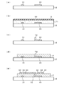
- FIG. 6 is a process diagram in which contact holes are formed according to a preferred embodiment of the present invention. It is a figure which shows the formation method of the contact hole by a conventional method.
- FIG. 1 and FIG. 2 show a circuit board 2 for an organic EL display device.
- FIG. 1 shows a plan view and a side view (portion of an organic transistor) of the circuit board 2
- FIG. 2 shows a circuit diagram.
- the circuit board 2 includes two organic transistors (Tr1) 3 and (Tr2) 4 (for example, organic TFT) and an organic EL (electroluminescence) element 5 (light emitting element) (for example, an OLED or the like) and a charge holding capacitor (Cap) 6 (for example, a storage capacitor or the like) are formed to form a dot of the display device.
- a display area is configured by arranging a large number of dots in a matrix.
- the organic transistor 3 is a switching transistor
- the organic transistor 4 is a driving transistor.
- These elements formed on the circuit board 2 form a circuit as shown in FIG. 2 and are configured to actively drive the organic EL element 5. Note that the arrangement of each element shown in FIG. 1 is described as an example, and is not limited to this arrangement.
- the gate electrode 31 of the switching organic transistor 3 is connected to the scan line (Vscan), and the source electrode 32 is connected to the data line (Vdata). Further, the drain electrode 33 is connected to the gate electrode 41 of the driving organic transistor 4 and to one terminal of the capacitor 6 of the capacitance line (Vcap).
- the source electrode 42 of the driving organic transistor 4 is connected to the low potential side power supply line (Vss). Furthermore, the anode terminal of the organic EL element 5 is connected to the drain electrode 43 of the organic transistor 4 for driving.
- reference numerals 34 and 44 in FIG. 1 denote organic semiconductor layers.
- a contact hole 7 as shown in FIG. 1B is formed in the insulating film (gate insulating film) 8.
- a liquid repellent photosensitive resin containing a conductive material or a mixture of a liquid repellent component mixed with a photosensitive resin containing a conductive material is used as a material for forming the conductive portion of the contact hole 7.
- the said photosensitive resin is apply
- the insulating film 8 is also formed by the wet process, thereby realizing the formation of the contact hole structure in the reverse order. .
- any one of a conductive nanotube, metal fine particles, and a conductive polymer, or a mixture of two or more types can be used.
- the conductive nanotube only needs to have conductivity, and the size and type thereof are not particularly limited.
- a carbon nanotube is preferable.
- the structure may be either a single layer structure or a multilayer structure, and may be either a structure with a closed tip or an open structure.
- a conductor or a semiconductor may be used.
- a preferable blending ratio of the conductive nanotubes is 1 to 50% by mass, preferably 1 to 25% by mass. Since the nanotubes have an elongated shape, there is an advantage that the contact rate between the nanotubes in the photosensitive resin is increased and it is easy to ensure conduction.
- the type of metal fine particles is not particularly limited as long as it is conductive metal fine particles.
- Preferable examples include fine particles of any one of Ag, Au, Cu, Cr, Fe, Zn, Al, Pt, ZuO, SnO, IZO, and ITO, or a mixture of two or more fine particles.
- the size of the metal fine particles is not particularly limited, but is preferably fine to ensure conduction, and it is preferable to use nanoparticles or microparticles. More preferred are fine particles having a particle size of 1 to 100 nm.
- a preferable blending ratio of metal fine particles that can provide sufficient conduction and can be patterned can be 50 to 90% by mass.
- the type of the conductive polymer is not particularly limited as long as it is a conductive polymer.
- Preferred conductive polymers include conjugated polymer compounds such as PEDOT / PSS, polyacetylene, polyparaphenylene, polyaniline, polythiophene, and polyparaphenylene vinylene. Further, a preferable blending ratio of the conductive polymer can be 50 to 90% by mass.
- a photoresist As the photosensitive resin containing (dispersing) the above-described conductive material, a photoresist can be cited as an example.
- the photosensitive property may be either positive or negative, and a chemically amplified resist can also be used.
- the resin is not particularly limited as long as it can form a pattern by being exposed to light.
- Preferable examples include acrylic resin, epoxy resin, polyimide resin and the like.
- the photosensitive resin used for this embodiment has a liquid-repellent property.
- liquid repellent photosensitive resin having a liquid repellent molecule such as a fluorine component in the molecular structure of the photosensitive resin, or a photosensitive resin mixed with a liquid repellent component such as a fluorine component.
- a liquid repellent photosensitive material containing a conductive material is mixed by mixing a large number of conductive materials in a solvent in which a liquid repellent photosensitive resin or a photosensitive resin mixed with a liquid repellent component is dissolved. You may make it prepare the mixture which mixed the liquid repellent component with resin or the photosensitive resin containing an electroconductive material. Of course, it may be prepared by other methods.
- the type of the solvent is not particularly limited, and an example is propylene glycol monomethyl ether acetate (PGMEA).
- PMEA propylene glycol monomethyl ether acetate
- the conductive material and the photosensitive resin, and in the case of further addition, the liquid repellent component may be used as a main component, and the addition of other components is not limited.
- a dispersant for suppressing aggregation of the fine particles can be added.
- One example thereof is modifying the surface of the fine particles with a thiol compound or a silane coupling agent.
- the material of the insulating film used in this embodiment may be formed by a wet process such as a coating method, and any insulating material can be used as long as this condition is satisfied.
- a wet process such as a coating method
- any insulating material can be used as long as this condition is satisfied.
- preferred examples include an aqueous solution containing polyvinyl alcohol (PVA), a PGMEA solution of polyvinyl phenol, and the like.
- FIG. 3 schematically shows a cross section of the substrate in the main process.
- a lower electrode is formed as a first conductive member on the substrate 2.
- the gate electrodes (31, 41) of the organic transistors 3 and 4 are formed.
- the lower electrode, the scan line, and the capacitance line of the capacitor 6 can be formed in this step.
- the electrode forming method include a sputtering method and an electroless plating method. However, it is not limited to this, and any film forming method may be used.
- the electrode material is not particularly limited, but as an example, Pt, Au, W, Ru, Ir, Al, Sc, Ti, V, Mn, Fe, Co, Ni, Zn, Ga, Y, Zr Nb, Mo, Tc, Rh, Pd, Ag, Cd, Ln, Sn, Ta, Re, Os, Tl, Pb, La, Ce, Pr, Nd, Pm, Sm, Eu, Gd, Tb, Dy, Ho , Er, Tm, Yb, Lu and other metal or combinations thereof, organic conductive materials including conjugated polymer compounds such as metal oxides such as ITO and IZO, polyanilines, polythiophenes and polypyrroles be able to.
- the substrate 2 include a glass substrate and a plastic substrate.
- a liquid-repellent photosensitive material containing a conductive material on the substrate 2 on which the gate electrodes (31, 41) are formed that is, a base surface on which a conductive portion is formed.
- a mixture of a resin or a photosensitive resin containing a conductive material mixed with a liquid repellent component is applied and dried to form a coating film 71.
- a known resist is applied on the coating film 71 and dried to form a resist film 9.
- An example of the coating method is a spin coating method. However, it is not limited to this, and any coating method may be used.
- an opening 91 of the resist film 9 is formed at a position where a conductive portion of the contact hole is to be formed.
- a known photolithography method such as electron beam drawing can be employed.
- the resist film 9 in which the opening 91 is formed is used as a mask to irradiate light to the lower layer film 71 and develop the conductive film at a position corresponding to the opening 91.
- a conductive portion 72 made of a liquid repellent photosensitive resin containing a conductive material or a mixture of a liquid repellent component mixed with a photosensitive resin containing a conductive material is formed.
- a baking process is performed by heating at a temperature corresponding to the type of resin, and the resin of the conductive portion 72 is cured.
- the film 71 can be irradiated with light by using a light source such as ultra-high pressure mercury as an example.
- the substrate 2 on which the conductive portion 71 and the gate electrodes (31, 41) are formed that is, the ground surface on which the conductive portion and the first conductive member are formed.
- an insulating material for example, 10% aqueous solution of PVA
- the insulating film 8 can be a dielectric of the capacitor 6 as well as the gate insulating films of the transistors 3 and 4.
- the insulating material is not limited to PVA, and other polymers having insulating properties can also be used.
- the coating method include spin coating and the like. However, it is not limited to this, and any coating method may be used.
- an upper electrode as a second conductive member is formed on the insulating film 8.
- the source electrodes (32, 42) and drain electrodes (42, 43) of the organic transistors 3 and 4; the upper electrode of the capacitor 6 (not shown); the data line and the power line; Wires to be connected are formed in a lump.
- the electrode forming method include a sputtering method and an electroless plating method. However, it is not limited to this, and any film forming method may be used. Further, the electrode material is not particularly limited, and the same material as the above-described gate electrode can be used. In the example of FIG. 3, the electrodes and wirings are formed in a lump in order to simplify the process, but each electrode or wiring may be formed in a separate process.
- the channel portions of the source electrode (32, 42) and the drain electrode (33, 43) for example, poly-3-hexylthiophene (P3HT), poly [9,9-dioctylfluorene-co-bithiophene]
- An organic semiconductor material such as (F8T2) is applied and dried to form the organic semiconductor layers (34, 44).
- the organic semiconductor material may be applied by an inkjet method.
- the bank may be formed so as to surround a region where the organic semiconductor material is applied.
- the lower electrode, the organic EL layer, and the upper electrode of the organic EL element 5 are sequentially formed at predetermined positions and sealed with an inorganic material. Through such steps, the circuit board 2 for the organic EL display device having the organic transistors 3 and 4 is formed.
- the liquid repellent photosensitive resin containing a fine conductive material or the photosensitive resin containing a fine conductive material as a material for forming the conductive portion 72 of the contact hole 7 is liquid repellent.
- the mixture in which the components are mixed to form a coating film 71 on the substrate 2 and patterning by irradiating light it is possible to form a conductive portion 72 having a desired size at a desired position.
- the insulating film 8 is similarly formed by the wet process. Wiring can be formed.
- power consumption can be reduced by the amount corresponding to the elimination of the etching and ashing steps, which can contribute to the reduction of CO 2 emissions.
- the upper surface and the periphery of the conductive portion 72 can be prevented from being covered with an insulating material. If the upper surface of the conductive portion 72 is covered with an insulating material, an insulating material is interposed between the upper electrode and the conductive material 72, and sufficient conduction may not be obtained. Therefore, in the present embodiment, by using a photosensitive resin having liquid repellency, the upper surface of the conductive portion 72 is prevented from being covered with an insulating material.
- the conductive portion 72 of the contact hole 7 is formed first, and then the insulating film 8 is formed, thereby preventing problems due to thermal contraction of the conductive portion 72 formed by the wet process. It becomes possible. That is, when a hole is formed in the insulating film in accordance with the conventional method and a conductive material is injected into the hole by a wet process to form the conductive portion 72, the conductive portion 72 is thermally shrunk by drying or baking, and the hole is formed in the hole. In some cases, a cavity is formed, or the upper surface of the conductive portion 72 is lower than the surface of the insulating film.
- the wiring of the contact hole structure can be formed by a series of wet processes. Therefore, this method is applied to the formation of a circuit substrate having an organic transistor, and can be manufactured by a simple method such as a wet process. It is possible to take advantage of the organic transistor fabrication aspect that it is possible. That is, the contact hole forming method according to the present embodiment is suitable for forming a circuit board having an organic transistor.
- the conductive portion 72 is formed by the process shown in FIG. 3C, and then a sintering process is performed to remove the metal fine particles in the conductive portion 72.
- a sintering process is performed to remove the metal fine particles in the conductive portion 72.
- the temperature for sintering varies depending on the type of metal, but it is usually an example that the temperature is about 80% of the melting temperature of the metal. For example, in the case of Ag, the temperature is 200 to 250 ° C. Except for performing the sintering treatment, the other steps can be performed in the same manner as in the above-described embodiment. Thus, by performing the sintering process, it becomes possible to ensure conduction more reliably.
- UV treatment or a combination of UV treatment and ozone treatment is performed, so that all or one of the organic substances contained in the conductive portion 72 is obtained.
- the part may be disassembled and removed.
- the circuit board 2 for an organic EL display device as shown in FIG. 1 is taken as an example.
- the circuit board 2 is not limited to this, and a liquid crystal display or electronic paper is used.
- a circuit board having an organic transistor such as a general circuit board as shown in FIG. That is, the contact hole forming method according to the present embodiment can be applied to all substrates having contact holes.
- a contact hole structure wiring is formed.
- a liquid repellent photosensitive resin containing a conductive material, or a liquid repellent component in a photosensitive resin containing a conductive material can also be used as a wiring material other than contact holes. In this case, it does not necessarily have liquid repellency.
- a top contact type organic transistor is described, but the structure is not limited to this structure.
- a bottom contact type or top gate type organic transistor may be used.
- it is not necessarily an organic transistor and may be an inorganic transistor.
- a mixture of Ag particles in a fluorine-containing acrylic photoresist was applied by spin coating on a glass substrate on which a transistor electrode and a capacitor electrode pattern were formed.
- the unexposed portion was removed and baked at 220 ° C. to form a conductive portion.
- a polyvinyl alcohol (PVA) 10% aqueous solution was applied to the glass substrate by spin coating as an insulating film material. Since the conducting portion was water-repellent, no PVA remained on the upper surface of the conducting portion.
- an electrode was produced by sputtering to ensure conduction between the transistors and form a circuit.
Landscapes
- Engineering & Computer Science (AREA)
- Manufacturing & Machinery (AREA)
- Microelectronics & Electronic Packaging (AREA)
- Thin Film Transistor (AREA)
- Internal Circuitry In Semiconductor Integrated Circuit Devices (AREA)
Abstract
L'invention a pour objet de former un câblage d'une structure de trou de contact par un processus humide simple. A cette fin, on applique sur une surface de base (2), sur laquelle sont formés des premiers éléments conducteurs (31, 41), une résine photosensible obtenue en mélangeant une résine photosensible repoussant les liquides ou un composant repoussant les liquides et contenant un matériau conducteur de manière à former un film de revêtement (71). On dessine le film de revêtement (71) par photolithographie de manière à former une partie conductrice (72) d'un trou de contact. On applique ensuite un matériau isolant sur la surface de base sur laquelle sont formés la partie conductrice (72) du trou de contact et les premiers éléments conducteurs (31, 41), ceci de manière à former un film isolant (8). Enfin, des seconds éléments conducteurs (32, 33, 42, 43) sont formés sur le film isolant (8).
Priority Applications (1)
| Application Number | Priority Date | Filing Date | Title |
|---|---|---|---|
| PCT/JP2008/063138 WO2010010609A1 (fr) | 2008-07-22 | 2008-07-22 | Procédé de formation de trou de contact et carte de circuit |
Applications Claiming Priority (1)
| Application Number | Priority Date | Filing Date | Title |
|---|---|---|---|
| PCT/JP2008/063138 WO2010010609A1 (fr) | 2008-07-22 | 2008-07-22 | Procédé de formation de trou de contact et carte de circuit |
Publications (1)
| Publication Number | Publication Date |
|---|---|
| WO2010010609A1 true WO2010010609A1 (fr) | 2010-01-28 |
Family
ID=41570087
Family Applications (1)
| Application Number | Title | Priority Date | Filing Date |
|---|---|---|---|
| PCT/JP2008/063138 Ceased WO2010010609A1 (fr) | 2008-07-22 | 2008-07-22 | Procédé de formation de trou de contact et carte de circuit |
Country Status (1)
| Country | Link |
|---|---|
| WO (1) | WO2010010609A1 (fr) |
Cited By (3)
| Publication number | Priority date | Publication date | Assignee | Title |
|---|---|---|---|---|
| WO2015199120A1 (fr) * | 2014-06-24 | 2015-12-30 | 大日本印刷株式会社 | Procede de production d'un element de cablage multicouche, procede de fabrication d'un element a semi-conducteur, element de cablage multicouche et element a semi-conducteur |
| WO2016098860A1 (fr) * | 2014-12-19 | 2016-06-23 | 出光興産株式会社 | Composition d'encre conductrice, élément de câblage stratifié, élément semi-conducteur et dispositif électronique, et procédé pour la production d'élément de câblage stratifié |
| US12229928B2 (en) | 2011-09-27 | 2025-02-18 | Koninklijke Philips N.V. | Apparatus and method for dynamic range transforming of images |
Citations (8)
| Publication number | Priority date | Publication date | Assignee | Title |
|---|---|---|---|---|
| JPH1070369A (ja) * | 1996-08-26 | 1998-03-10 | Matsushita Electric Works Ltd | 多層プリント配線板の製造方法 |
| JP2000305260A (ja) * | 1999-04-26 | 2000-11-02 | Toray Ind Inc | 感光性導体ペースト |
| JP2002093314A (ja) * | 2000-09-11 | 2002-03-29 | Matsushita Electric Ind Co Ltd | 厚膜形成方法および厚膜形成装置 |
| JP2005051106A (ja) * | 2003-07-30 | 2005-02-24 | Seiko Epson Corp | 多層配線の形成方法、多層配線基板の製造方法 |
| JP2007148386A (ja) * | 2005-10-25 | 2007-06-14 | Toray Ind Inc | 配線パターン印刷用水なし平版印刷版原版およびそれを用いた配線パターン |
| JP2007533117A (ja) * | 2004-04-30 | 2007-11-15 | シャープ株式会社 | 素子配置基板及びその製造方法 |
| JP2007324201A (ja) * | 2006-05-30 | 2007-12-13 | Hitachi Ltd | 有機薄膜トランジスタを有する半導体装置の製造方法 |
| JP2007335773A (ja) * | 2006-06-19 | 2007-12-27 | Sony Corp | 半導体装置の製造方法 |
-
2008
- 2008-07-22 WO PCT/JP2008/063138 patent/WO2010010609A1/fr not_active Ceased
Patent Citations (8)
| Publication number | Priority date | Publication date | Assignee | Title |
|---|---|---|---|---|
| JPH1070369A (ja) * | 1996-08-26 | 1998-03-10 | Matsushita Electric Works Ltd | 多層プリント配線板の製造方法 |
| JP2000305260A (ja) * | 1999-04-26 | 2000-11-02 | Toray Ind Inc | 感光性導体ペースト |
| JP2002093314A (ja) * | 2000-09-11 | 2002-03-29 | Matsushita Electric Ind Co Ltd | 厚膜形成方法および厚膜形成装置 |
| JP2005051106A (ja) * | 2003-07-30 | 2005-02-24 | Seiko Epson Corp | 多層配線の形成方法、多層配線基板の製造方法 |
| JP2007533117A (ja) * | 2004-04-30 | 2007-11-15 | シャープ株式会社 | 素子配置基板及びその製造方法 |
| JP2007148386A (ja) * | 2005-10-25 | 2007-06-14 | Toray Ind Inc | 配線パターン印刷用水なし平版印刷版原版およびそれを用いた配線パターン |
| JP2007324201A (ja) * | 2006-05-30 | 2007-12-13 | Hitachi Ltd | 有機薄膜トランジスタを有する半導体装置の製造方法 |
| JP2007335773A (ja) * | 2006-06-19 | 2007-12-27 | Sony Corp | 半導体装置の製造方法 |
Cited By (8)
| Publication number | Priority date | Publication date | Assignee | Title |
|---|---|---|---|---|
| US12229928B2 (en) | 2011-09-27 | 2025-02-18 | Koninklijke Philips N.V. | Apparatus and method for dynamic range transforming of images |
| WO2015199120A1 (fr) * | 2014-06-24 | 2015-12-30 | 大日本印刷株式会社 | Procede de production d'un element de cablage multicouche, procede de fabrication d'un element a semi-conducteur, element de cablage multicouche et element a semi-conducteur |
| JP2016027631A (ja) * | 2014-06-24 | 2016-02-18 | 大日本印刷株式会社 | 積層配線部材の製造方法、半導体素子の製造方法、積層配線部材および半導体素子 |
| WO2016098860A1 (fr) * | 2014-12-19 | 2016-06-23 | 出光興産株式会社 | Composition d'encre conductrice, élément de câblage stratifié, élément semi-conducteur et dispositif électronique, et procédé pour la production d'élément de câblage stratifié |
| JP2016119474A (ja) * | 2014-12-19 | 2016-06-30 | 出光興産株式会社 | 導体組成物インク、積層配線部材、半導体素子および電子機器、並びに、積層配線部材の製造方法 |
| CN107004637A (zh) * | 2014-12-19 | 2017-08-01 | 出光兴产株式会社 | 导体组合物油墨、层叠布线构件、半导体元件和电子设备以及层叠布线构件的制造方法 |
| US10026624B2 (en) | 2014-12-19 | 2018-07-17 | Idemitsu Kosan Co., Ltd. | Conductor composition ink, laminated wiring member, semiconductor element and electronic device, and method for producing laminated wiring member |
| CN107004637B (zh) * | 2014-12-19 | 2018-12-25 | 出光兴产株式会社 | 层叠布线构件及制造方法、油墨、半导体元件和电子设备 |
Similar Documents
| Publication | Publication Date | Title |
|---|---|---|
| JP4100351B2 (ja) | 薄膜トランジスタの製造方法 | |
| US8188465B2 (en) | Method of manufacturing semiconductor device, semiconductor device, display device, and electronic instrument | |
| US8227294B2 (en) | Manufacturing method of semiconductor device | |
| CN101223645B (zh) | 有机薄膜晶体管和有源矩阵显示器 | |
| CN101627464B (zh) | 层叠结构体及其制造方法 | |
| CN101083305B (zh) | 具有有机薄膜晶体管的半导体器件的制造方法 | |
| JP5256676B2 (ja) | 有機半導体素子、有機半導体素子の製造方法、有機トランジスタアレイ、およびディスプレイ | |
| JP5025110B2 (ja) | 半導体装置の作製方法 | |
| JP5168845B2 (ja) | 積層構造体、積層構造体を用いた電子素子、これらの製造方法、電子素子アレイ及び表示装置 | |
| JP2009087996A (ja) | 有機半導体素子、有機半導体素子の製造方法、有機トランジスタアレイ、およびディスプレイ | |
| JP5250981B2 (ja) | 有機デバイスの製造方法並びに電子機器 | |
| JP5870502B2 (ja) | 有機半導体素子およびその製造方法 | |
| JP2005251809A (ja) | 薄膜トランジスタの製造方法、薄膜トランジスタ、薄膜トランジスタ回路、電子デバイスおよび電子機器 | |
| JP5729540B2 (ja) | 電界効果型トランジスタ及びその製造方法 | |
| JP6160361B2 (ja) | 有機半導体素子およびその製造方法 | |
| JP5181586B2 (ja) | 有機半導体素子、有機半導体素子の製造方法、有機トランジスタアレイ、およびディスプレイ | |
| JP6277625B2 (ja) | 有機半導体素子およびその製造方法 | |
| JP2016001689A (ja) | 有機半導体素子 | |
| JP2007227595A (ja) | 有機薄膜トランジスタの製造方法 | |
| JP5205894B2 (ja) | 有機半導体素子、有機半導体素子の製造方法、有機トランジスタアレイ、およびディスプレイ | |
| JP6435651B2 (ja) | 有機半導体素子 | |
| JP2008109116A (ja) | 有機半導体素子、有機半導体素子の製造方法、有機トランジスタアレイ、およびディスプレイ | |
| JP2008084941A (ja) | 有機半導体素子の製造方法 |
Legal Events
| Date | Code | Title | Description |
|---|---|---|---|
| 121 | Ep: the epo has been informed by wipo that ep was designated in this application |
Ref document number: 08791419 Country of ref document: EP Kind code of ref document: A1 |
|
| NENP | Non-entry into the national phase |
Ref country code: DE |
|
| 122 | Ep: pct application non-entry in european phase |
Ref document number: 08791419 Country of ref document: EP Kind code of ref document: A1 |
|
| NENP | Non-entry into the national phase |
Ref country code: JP |