WO2010010706A1 - レジストトリミング方法及びトリミング装置 - Google Patents
レジストトリミング方法及びトリミング装置 Download PDFInfo
- Publication number
- WO2010010706A1 WO2010010706A1 PCT/JP2009/003463 JP2009003463W WO2010010706A1 WO 2010010706 A1 WO2010010706 A1 WO 2010010706A1 JP 2009003463 W JP2009003463 W JP 2009003463W WO 2010010706 A1 WO2010010706 A1 WO 2010010706A1
- Authority
- WO
- WIPO (PCT)
- Prior art keywords
- trimming
- plasma
- space
- resist
- resist pattern
- Prior art date
- Legal status (The legal status is an assumption and is not a legal conclusion. Google has not performed a legal analysis and makes no representation as to the accuracy of the status listed.)
- Ceased
Links
Images






Classifications
-
- H—ELECTRICITY
- H10—SEMICONDUCTOR DEVICES; ELECTRIC SOLID-STATE DEVICES NOT OTHERWISE PROVIDED FOR
- H10P—GENERIC PROCESSES OR APPARATUS FOR THE MANUFACTURE OR TREATMENT OF DEVICES COVERED BY CLASS H10
- H10P50/00—Etching of wafers, substrates or parts of devices
- H10P50/20—Dry etching; Plasma etching; Reactive-ion etching
- H10P50/28—Dry etching; Plasma etching; Reactive-ion etching of insulating materials
- H10P50/286—Dry etching; Plasma etching; Reactive-ion etching of insulating materials of organic materials
- H10P50/287—Dry etching; Plasma etching; Reactive-ion etching of insulating materials of organic materials by chemical means
-
- G—PHYSICS
- G03—PHOTOGRAPHY; CINEMATOGRAPHY; ANALOGOUS TECHNIQUES USING WAVES OTHER THAN OPTICAL WAVES; ELECTROGRAPHY; HOLOGRAPHY
- G03F—PHOTOMECHANICAL PRODUCTION OF TEXTURED OR PATTERNED SURFACES, e.g. FOR PRINTING, FOR PROCESSING OF SEMICONDUCTOR DEVICES; MATERIALS THEREFOR; ORIGINALS THEREFOR; APPARATUS SPECIALLY ADAPTED THEREFOR
- G03F7/00—Photomechanical, e.g. photolithographic, production of textured or patterned surfaces, e.g. printing surfaces; Materials therefor, e.g. comprising photoresists; Apparatus specially adapted therefor
- G03F7/26—Processing photosensitive materials; Apparatus therefor
- G03F7/40—Treatment after imagewise removal, e.g. baking
Definitions
- the present invention relates to a resist trimming method and a trimming apparatus for forming an ultrafine resist pattern below the resolution limit of an exposure apparatus.
- the pattern size has been miniaturized. Since the speed performance of a semiconductor device is mainly determined by the width dimension of a circuit pattern when the materials are the same, miniaturization has been promoted year by year, and a precise exposure process is required accordingly.
- the miniaturization capability of the exposure process mainly depends on the wavelength of the exposure light source
- the development of resist materials sensitive to the wavelength from the I-line to the KrF laser, ArF laser, the shorter wavelength light source and the wavelength has been advanced.
- the shortening of the wavelength of the light source has not caught up with the progress of miniaturization, and the pattern transfer capability has reached its limit, and it is difficult to perform miniaturization in generations with a gate length of 32 nm or later.
- a technique called resist trimming in which an etching gas such as oxygen is introduced into a vacuum processing chamber, a plasma discharge is generated under reduced pressure, and plasma processing is performed to narrow the width of the resist pattern. (See Patent Document 1).
- resist trimming using capacitively coupled plasma as shown in Patent Document 1 has the following problems.
- the resist etching rate that is, the trimming rate is too high, from several hundred to several thousand nm / min. It is difficult to control the dimensions of several tens to several nanometers.
- the high-density plasma is directly irradiated onto the substrate, which may cause charge-up damage to the processing substrate.
- the ion density is high, it is difficult to perform isotropic etching by ion bombardment. For example, if the pattern width is intended, the pattern thickness may become too small.
- the present invention has been proposed in view of the above-described problems, and an object of the present invention is to provide a resist trimming method and a trimming apparatus capable of controlling dimensions with high accuracy by performing resist trimming at a low trimming speed.
- the resist trimming method of the present invention includes the following steps in order to achieve the above-described object.
- the first step is a plasma generation step for generating a reactive gas plasma.
- the second step is a removal step in which ions and electrons are removed from the generated plasma to selectively extract radicals.
- the third step is a trimming step for trimming the resist pattern by irradiating the resist pattern with plasma from which ions and electrons have been removed.
- resist trimming can be performed at a low trimming speed, dimensions can be controlled with high accuracy.
- FIG. 6 is a diagram illustrating a result of evaluating charge-up damage by measuring the IV characteristics of a MOS capacitor (Example 2 / leakage current). The result figure which evaluated the charge-up damage by the measurement of the IV characteristic of a MOS capacitor (Example 2 / breakdown voltage). The result figure which evaluated the charge-up damage by the measurement of the IV characteristic of a MOS capacitor (comparative example / leakage current).
- a trimming apparatus includes a plasma generation space in which a high-frequency electrode is disposed, a trimming processing space in which an object to be processed can be disposed, a conductive member, a gas introduction unit, an exhaust unit, and a high-frequency power supply unit. And a controller.
- the conductive member is disposed between the plasma generation space and the trimming processing space, and has a plurality of through holes for communicating both spaces.
- the gas introduction means introduces a reaction gas into the plasma generation space.
- the exhaust means exhausts the plasma generation space and the trimming processing space.
- the high frequency power supply means supplies power to the high frequency electrode.
- the controller controls the gas introduction unit, the exhaust unit, and the high frequency power supply unit to introduce the plasma from which ions and electrons have been removed into the trimming process space and trim the resist pattern introduced into the trimming process space.
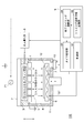
- FIG. 1 is a schematic diagram illustrating a configuration of a trimming apparatus according to the present embodiment.
- a trimming apparatus 100 includes a vacuum container 11 that can keep the inside in a vacuum state.
- a partition plate 1 made of a conductive member (SUS or aluminum) is provided in a horizontal state.
- the vacuum vessel 11 is grounded by the partition plate 1 and is divided into a plasma generation chamber 3 that forms a plasma discharge space that functions as a plasma generation space, and a trimming processing chamber 4 that functions as a trimming processing space.
- the partition plate 1 is formed with a plurality of through holes 5 penetrating the plasma generation chamber 3 and the trimming chamber 4 in the vertical direction, thereby blocking electrons and ions.
- a trimming gas that is a reactive gas is introduced into the plasma generation chamber 3, and high frequency power (for example, 13.56 MHz) is supplied to the high frequency electrode 2 from the high frequency power supply 21 that functions as a high frequency power supply means, thereby capacitively coupled plasma. Is born.
- a substrate holding mechanism 6 capable of holding the substrate 12 by an electrostatic adsorption action or the like is disposed.
- a heater 7 is provided inside the substrate holding mechanism 6, and it is possible to uniformly control the substrate temperature by this heater 7 and keep the trimming distribution uniform. It is possible to obtain a trimming shape with a good in-plane distribution by attaching a heater to the entire interior of the partition plate 1 and the vacuum container 11 to uniformly control the temperature of the entire vacuum container 11.
- the gas introduction system 8 that functions as a gas introduction means introduces gas from a gas supply source to the plasma generation chamber 3, has a mass flow controller (not shown), and is based on a command from the controller 9.
- the flow rate introduced into the can be adjusted.
- Trimming gas introduced from the gas introduction system 8 includes O atom, H atom, N atom as a substance that can convert C, H, O, etc. into a component such as CO2 by reaction with an organic compound as a constituent material of the photoresist.
- a gas containing the above can be used. Radicals containing O atoms can be suitably used because of their high reactivity. For example, C atoms in a photoresist are converted into components such as carbon dioxide.
- radicals containing H atoms react with C atoms in the photoresist and are converted into components such as CHX.
- CHX For example, O2, O3, N2, NH3, H2, NOX, CXHY (X and Y are arbitrary numbers, for example, alkanes such as methane and ethane, alkynes such as ethylene), CXHYOZ (X, Y, and Z are arbitrary)
- alcohols such as CH 3 OH
- ketones such as methyl ethyl ketone, isopropyl methyl ketone, and methyl propyl ketone
- aldehydes carboxylic acids, ethers, and esters
- plasma serving as a radical generation source is generated in the plasma generation chamber 3.
- the plasma contains electrons, radicals, and ions, but the electrons and ions are blocked by the partition plate 1 charged by high-frequency discharge, and the radicals are selectively introduced into the trimming chamber 4 through the through-holes 5 to form the substrate 12.
- oxygen plasma is generated.
- oxygen radicals pass through the through holes 5 and are separated and introduced into the trimming process chamber 4, and the process substrate 12 is irradiated with oxygen radicals.
- the oxygen radicals are combined with C atoms in the photoresist to become CO2 or CO, or are combined with H atoms and converted to H2O or the like.
- the gas flow rate in the through hole 5 of the partition plate 1 is u
- the substantial length of the through hole 5 is L
- the mutual gas diffusion coefficient is D, uL / D>
- the length L of the through hole 5 and the gas flow rate u are set so as to satisfy the condition of 1. Thereby, the reverse diffusion of radicals from the partition plate 1 to the plasma generation chamber 3 is prevented.
- the diameter size of the through holes 5 and the number of the through holes 5 in the partition plate 1 are also related to the amount of electrons and ions blocked, and are set so that the electron density in the trimming processing chamber 4 is set to a target value.
- the exhaust system 10 that functions as an exhaust means is configured to include a turbo molecular pump (not shown) and the like, and exhausts the trimming processing chamber 4 at a predetermined exhaust speed based on a command from the controller 9.
- the controller 9 can control process conditions such as high-frequency power, gas flow rate, process pressure, processing time, and substrate temperature by sending commands to the high-frequency power source 21, the gas introduction system 8, the exhaust system 10, the heater 7, and the like. ing.
- the process pressure is set to a predetermined value by controlling at least one of the gas introduction system 8 and the exhaust system 10 based on an input from a pressure sensor (not shown).
- the controller 9 includes a general computer, a driver that can transmit commands to various devices, and the like, and executes trimming processing based on a program.
- the controller 9 having such a configuration includes a control unit 91, It functions as a timer processing unit 92, a trimming speed information storage unit 93, and an end timing calculation unit 94.
- the control unit 91 is a functional unit that controls the controller 9 in an integrated manner.
- the timer processing unit 92 is a functional unit for ending the trimming process when the resist pattern is trimmed to a desired size.
- the trimming speed information storage unit 93 is a functional unit for storing trimming speed information related to the trimming speed.
- the end timing calculation unit 94 is a functional unit for determining the end timing of the trimming process based on the trimming speed information.
- the resist trimming method includes the following three steps as main steps.
- the first step is a plasma generation step for generating plasma of a reactive gas.
- the second step is a removal step in which ions and electrons are removed from the generated plasma to selectively extract radicals.
- the third step is a trimming step for trimming the resist pattern by irradiating the resist pattern with plasma from which ions and electrons have been removed.
- plasma is generated by introducing a reactive gas into the plasma generation space, supplying high frequency power to the high frequency electrode, and causing high frequency discharge. Then, the generated plasma is introduced into the trimming processing space via a conductive member, so that the plasma from which ions and electrons are removed is irradiated.
- FIGS. 2A and 2B are explanatory views showing a resist trimming method according to this embodiment.
- the substrate (the substrate portion is not shown) on which the material to be etched 31 and the resist pattern are stacked is placed in the trimming processing chamber 4 in a state where the inside of the vacuum vessel 11 is maintained at a predetermined degree of vacuum. It is carried in and placed on the substrate holding mechanism 6. Then, a trimming gas is introduced into the plasma generation chamber 3 and high frequency power is applied to the high frequency electrode 2 to generate plasma. Plasma diffuses toward the trimming chamber 4, but ions and electrons are blocked by the partition plate 1, and only radicals of trimming gas molecules are introduced into the trimming chamber 4, and the electron density in the trimming chamber 4 is 1 ⁇ . It is maintained at 10 +7 cm ⁇ 3 or less.
- the surface of the photoresist 32 When exposed to radicals of trimming gas molecules, the surface of the photoresist 32 is oxidized and converted into gas molecules such as carbon dioxide, and the size of the resist pattern is reduced as shown in FIG. 2B.
- the power supply to the high-frequency electrode 2 is stopped to end the trimming process. For example, when a predetermined processing time elapses, the processing is terminated assuming that the desired size is reached.
- the predetermined processing time will be described with reference to FIG. FIG. 3 is a map showing the correspondence between the CD and the trimming time (in this example, the line width of the resist pattern).
- the predetermined processing time is a controller that maps a map showing the correspondence between the CD and the trimming time, corresponding to each process condition (trimming gas type, process pressure, substrate temperature, etc.) and each resist material. 9 and determine based on this.
- the processing time ⁇ t required to change from the line width CD 0 before processing to the target line width CD 1 is calculated based on the map, and the processing is terminated when the processing time ⁇ t has elapsed.
- a predetermined processing time may be calculated based on an approximate expression instead of a map, or appropriate correction may be performed.
- the electron density is 1 ⁇ 10 +7 cm ⁇ 3 or less, and the resist trimming can be performed at a low trimming speed by trimming the resist pattern using the trimming gas. For this reason, it becomes possible to control the dimensions with high accuracy at a level of several tens nm to several nm.
- the predetermined processing time described above is determined by calculation by the controller 9, but a predetermined value is inputted by the user, and only the timer processing (processing for sending an end signal when the predetermined time elapses) is performed by the controller. 9 may be executed.
- the end point is determined by timer processing, feedback control may be performed by detecting the actual value using a known film thickness detector or the like.
- the trimming speed can be made extremely low, so that a desired dimension can be obtained with high accuracy even by a method of determining the processing time based on the trimming speed, There are advantages that the end point detection is easy and the apparatus configuration can be simplified.
- the present invention is not limited to the embodiment described above.
- capacitively coupled plasma is generated in the above-described embodiment, an apparatus configuration that generates inductively coupled plasma may be used, or an apparatus configuration that generates ECR or helicon wave plasma may be used.
- Example 1 in order to confirm that the trimming apparatus 100 shown in FIG. 1 satisfies the requirements for electron density, an electron density measurement test of the trimming chamber 4 was performed.
- the electron density of the trimming processing chamber 4 was measured using a Langmuir probe to measure the saturation ion current density at a position 11 mm directly above the processing substrate.
- Oxygen 500 sccm was used as a trimming gas, and argon 50 sccm was used as a carrier gas.
- a power of 200 W was applied to the high-frequency electrode 2 provided in the plasma generation chamber 3.
- the process pressure was 20 Pa.
- FIG. 4 is an electron density measurement result diagram of Example 1. As shown in FIG. 4, the electron density was kept at 1 ⁇ 10 +7 cm ⁇ 3 or less, and it was confirmed that the electron density was lower by 3 digits or more than when the partition plate 1 was not used.
- Example 2 Next, as Example 2, a test for confirming the effect of reducing the charge-up damage was performed.
- Example 2 the MOS capacitor was processed using the same apparatus and process conditions as in Example 1.
- a similar test was performed on a capacitive coupling type device without the partition plate 1.
- the test was performed with the trimming gas as oxygen at 500 sccm, the pressure as 180 Pa, and the input power as 1000 W.
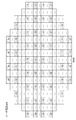
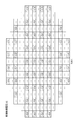
- FIG. 5 to 8 are graphs showing the results of evaluating the charge-up damage by measuring the IV characteristics of the MOS capacitor.
- the numerical values in FIG. 5 (Example 2) and FIG. 7 (Comparative Example) indicate the leakage current (pA) at each point.
- the absolute value of the leakage current value of the MOS capacitor is large.
- the numerical value in FIG. 6 (Example 2) and FIG. 8 (comparative example) has shown the breakdown voltage (V), and the absolute value of a breakdown voltage becomes small.
- Example 3 Next, as Example 3, the trimming speed was measured.
- Example 3 the substrate having a photoresist formed on the surface was processed and the trimming speed was measured using the same apparatus and process conditions as in Example 1. Further, as a comparative example, the substrate on which the photoresist was formed was processed under the same process conditions as in the comparative example in Example 1, and the trimming speed was measured.
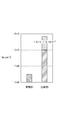
- FIG. 9 is a measurement result diagram of the trimming speed. As shown in FIG. 9, in the comparative example, the resist trimming speed is very high, 100 to 1000 nm / min. However, it is confirmed that the trimming speed is 10 nm / min or less in the resist trimming method using the radical of this embodiment. It was done.
- Example 4 Next, as Example 4, the resist trimming speed and in-plane distribution were measured by changing the substrate temperature and the process pressure.
- Oxygen 500 sccm was used as a trimming gas, and argon 50 sccm was used as a carrier gas. A power of 200 W was applied to the high-frequency electrode 2 provided in the plasma generation chamber 3.
- the process pressures in the plasma generation chamber 3 and the trimming chamber 4 are both 20 to 50 Pa, and the temperature of the processing substrate is 30 to 100 ° C., which is a low temperature region that does not affect the resist resistance.
- FIG. 10 is a measurement result diagram of the trimming speed and the temperature of the substrate holding mechanism.
- the resist trimming rate was 10 nm / min or less, and the trimming rate was kept low.
- FIG. 11 shows the process pressure and the in-plane distribution, and confirms the in-plane distribution on the 200 mm substrate.
- the maximum trimming distribution was 3 ⁇ and 5% or less.
- Example 5 Next, as Example 5, a test for confirming dimensional controllability was performed.
- the process gas used was 500 sccm of oxygen and 50 sccm of argon as the carrier gas.
- the high frequency electrode 2 disposed in the plasma generation chamber 3 was supplied with a power of 200 W.
- the process pressure of the plasma generation chamber 3 and the trimming chamber 4 was 50 Pa, and the temperature of the processing substrate was 100 ° C.
- CD measurement was performed on a trimming method using inductively coupled plasma in which plasma was irradiated as it was without selecting radicals.
- the process gas was oxygen 1 sccm, Ar 50 sccm, power 500 W, process pressure 1 Pa, and the processing substrate temperature was 80 ° C.
- FIG. 12 is a measurement result diagram of the resist pattern CD.
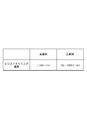
- the trimming method of the present embodiment can perform resist trimming with much higher accuracy of about 200 sec for performing 50 nm trimming.
- Example 6 Next, as Example 6, a test for confirming the isotropy of the trimming process was performed.
- Example 6 The process conditions of Example 6 and Comparative Example were the same as those of Example 5.
- FIG. 13 is a measurement result diagram of the amount of change in aspect ratio after resist trimming.
- the amount of change in the horizontal direction after resist trimming is A, and the amount of change in the vertical direction is B.
- the aspect ratio of trimming tends to be anisotropic due to ion bombardment and the like, but the ion trimming can be reduced and the aspect ratio can be trimmed isotropically by the resist trimming method of this embodiment.
Landscapes
- Physics & Mathematics (AREA)
- General Physics & Mathematics (AREA)
- Drying Of Semiconductors (AREA)
- Photosensitive Polymer And Photoresist Processing (AREA)
- Exposure Of Semiconductors, Excluding Electron Or Ion Beam Exposure (AREA)
Abstract
反応ガスのプラズマを生成するプラズマ生成工程と、生成したプラズマからイオン及び電子を除去し、ラジカルを選択的に取り出す除去工程と、イオン及び電子が除去されたプラズマをレジストパターンに照射することで、レジストパターンをトリミングするトリミング工程と、を含む。
Description
本発明は、露光装置の解像限界以下の超微細レジストパターンを形成するためのレジストトリミング方法及びトリミング装置に関する。
近年、半導体の高集積化及びチップサイズの縮小化に伴い、パターンサイズの微細化が推し進められている。半導体装置の速度性能は、材料が同じ場合には主に回路パターンの幅寸法によって決まるため、年々微細化が推し進められており、それに応じて精密な露光工程が要求される。
露光工程の微細化能力は、主に露光光源の波長に依存するため、I線からKrFレーザ、ArFレーザと、より短い波長の光源とその波長に感度のあるレジスト材料の開発が進められてきた。しかし、近年、光源の短波長化が微細化の進展に追いつかず、パターン転写能力が限界にきており、ゲート長32nm以降の世代では微細化を行うことが難しい。
そこで、露光によって形成できないような微細パターンについて、別の方法でレジストを変形させ、細らせて微細化する技術の開発が行われている。
このような技術として、例えば、真空処理室内に酸素等のエッチングガスを導入し、減圧下でプラズマ放電を発生させ、プラズマ処理を施してレジストパターンの幅を狭くするレジストトリミングという技術が開示されている(特許文献1参照)。
しかしながら、特許文献1に示すような容量結合型プラズマを利用したレジストトリミングでは、次のような問題があった。
第1に、プラズマの電子密度が1×10+10~10+12cm-3と非常に高いために、レジストのエッチング速度、即ちトリミング速度が数百から数千nm/minと速すぎて、数十nmから数nmレベルの寸法制御が難しい。
第2に、上述したように、プラズマの電子密度やイオン密度が高いと、高密度のプラズマが基板に直接照射されるために、処理基板へのチャージアップダメージを引き起こす可能性がある。
第3に、イオン密度が高いと、イオン衝撃により等方的なエッチングを行うことが難しく、例えば、目的のパターン幅にしようとすると、パターン厚さが小さくなりすぎてしまうことがある。
本発明は、上述した問題に鑑み提案されたもので、低いトリミング速度でレジストトリミングを実施することにより、高精度で寸法をコントロールすることが可能なレジストトリミング方法及びトリミング装置を提供することを目的とする。
本発明のレジストトリミング方法は、上述した目的を達成するため、以下の工程を含むことを特徴とする。
第1の工程は、反応ガスのプラズマを生成するプラズマ生成工程である。第2の工程は、生成したプラズマからイオン及び電子を除去し、ラジカルを選択的に取り出す除去工程である。第3の工程は、イオン及び電子が除去されたプラズマをレジストパターンに照射することで、レジストパターンをトリミングするトリミング工程である。
本発明によれば、低いトリミング速度でレジストトリミングを実施することができるため、高精度で寸法をコントロールすることが可能となる。
添付図面は明細書に含まれ、その一部を構成し、本発明の実施の形態を示し、その記述と共に本発明の原理を説明するために用いられる。
以下、本発明に係る一実施形態について図面を参照して詳細に説明する。なお、以下に説明する実施形態は、本発明の実現手段としての一例であり、本発明が適用される装置の構成や各種条件によって適宜修正又は変更されるべきものであり、本発明は以下の実施形態に限定されるものではない。
[トリミング装置の構成]
本発明に係るトリミング装置は、高周波電極が配置されたプラズマ生成空間と、被処理体を配置可能なトリミング処理空間と、導電性部材と、ガス導入手段と、排気手段と、高周波電力供給手段と、コントローラとを備えている。導電性部材は、プラズマ生成空間とトリミング処理空間との間に配されており、両空間を連通するための複数の貫通孔を有している。ガス導入手段は、プラズマ生成空間に反応ガスを導入する。排気手段は、プラズマ生成空間及びトリミング処理空間を排気する。高周波電力供給手段は、高周波電極への電力供給を行う。コントローラは、ガス導入手段、排気手段及び高周波電力供給手段を制御することで、イオン及び電子が除去されたプラズマをトリミング処理空間に導入し、当該トリミング処理空間に導入されたレジストパターンをトリミングする。
本発明に係るトリミング装置は、高周波電極が配置されたプラズマ生成空間と、被処理体を配置可能なトリミング処理空間と、導電性部材と、ガス導入手段と、排気手段と、高周波電力供給手段と、コントローラとを備えている。導電性部材は、プラズマ生成空間とトリミング処理空間との間に配されており、両空間を連通するための複数の貫通孔を有している。ガス導入手段は、プラズマ生成空間に反応ガスを導入する。排気手段は、プラズマ生成空間及びトリミング処理空間を排気する。高周波電力供給手段は、高周波電極への電力供給を行う。コントローラは、ガス導入手段、排気手段及び高周波電力供給手段を制御することで、イオン及び電子が除去されたプラズマをトリミング処理空間に導入し、当該トリミング処理空間に導入されたレジストパターンをトリミングする。
以下、図1を参照して、本実施形態に係るトリミング装置を具体的に説明する。図1は、本実施形態に係るトリミング装置の構成を示す概略図である。
図1に示すように、本実施形態に係るトリミング装置100は、内部を真空状態に保持可能な真空容器11を備えている。真空容器11の内部には、導電性部材(SUSやアルミニウム)からなる隔壁板1が、水平な状態で設けられている。真空容器11は、この隔壁板1によって接地されるとともに、プラズマ生成空間として機能するプラズマ放電空間を形成するプラズマ生成室3と、トリミング処理空間として機能するトリミング処理室4とに分けられている。この隔壁板1には、プラズマ生成室3とトリミング処理室4とを上下方向に貫通する複数の貫通孔5が形成されており、これにより電子やイオンを遮断する。また、プラズマ生成室3に反応ガスであるトリミングガスを導入し、高周波電力供給手段として機能する高周波電源21から高周波電極2に高周波電力(例えば、13.56MHz)を供給することで、容量結合プラズマが生起される。
トリミング処理室4には、静電吸着作用等により基板12を保持可能な基板保持機構6が配置されている。また、基板保持機構6の内部にはヒータ7が設けられており、このヒータ7によって基板温度を均一にコントロールし、トリミング分布を均一に保つことが可能である。なお、隔壁板1や真空容器11の内部全体にもヒータを取り付けて真空容器11の全体の温度を均一にコントロールすることにより、面内分布の良いトリミング形状を得ることが可能である。
ガス導入手段として機能するガス導入系8は、ガスの供給源からプラズマ生成室3にガスを導入するものであり、図示しないマスフローコントローラを有し、コントローラ9からの指令に基づいてプラズマ生成室3に導入する流量を調整可能になっている。ガス導入系8から導入するトリミングガスとしては、ホトレジストの構成材料となる有機化合物との反応により、C,H,OなどをCO2などの成分に変換可能な物質としてO原子、H原子、N原子などを含むガスを用いることができる。O原子を含むラジカルは反応性が高いため好適に用いることができ、例えば、ホトレジスト中のC原子を二酸化炭素などの成分
に変換する。また、H原子を含むラジカルは、ホトレジスト中のC原子と反応して、CHXなどの成分に変換する。例えば、O2、O3、N2、NH3、H2、NOX、CXHY(X,Yは任意の数、例えば、メタンやエタンなどのアルカン類、エチレンなどのアルキン類)、CXHYOZ(X,Y,Zは任意の数、例えば、アルコール類(CH3OH等)、ケトン類(メチルエチルケトン、イソプロピルメチルケトン、メチルプロピルケトン等)、アルデヒド類、カルボン酸類、エーテル類、エステル類)などを含むガスを用いることができる。
に変換する。また、H原子を含むラジカルは、ホトレジスト中のC原子と反応して、CHXなどの成分に変換する。例えば、O2、O3、N2、NH3、H2、NOX、CXHY(X,Yは任意の数、例えば、メタンやエタンなどのアルカン類、エチレンなどのアルキン類)、CXHYOZ(X,Y,Zは任意の数、例えば、アルコール類(CH3OH等)、ケトン類(メチルエチルケトン、イソプロピルメチルケトン、メチルプロピルケトン等)、アルデヒド類、カルボン酸類、エーテル類、エステル類)などを含むガスを用いることができる。
トリミングガスをプラズマ生成室3に導入した状態で、高周波電力を高周波電極2に供給すると、プラズマ生成室3でラジカル発生源となるプラズマが発生する。プラズマは、電子、ラジカル、イオンを含むが、高周波放電により帯電した隔壁板1によって電子やイオンは遮断され、ラジカルが選択的に貫通孔5を通過してトリミング処理室4に導入され、基板12に照射されることになる。例えば、酸素がプラズマ生成室3に導入された状態で高周波電力をプラズマ生成室3に供給すると、酸素プラズマが発生する。その内、酸素ラジカルのみが貫通孔5を通過して分離されてトリミング処理室4に導入され、酸素ラジカルが処理基板12に照射される。酸素ラジカルは、ホトレジスト中のC原子と結合してCO2やCOとなり、あるいはH原子と結合しH2Oなどに変換される。
なお、上記構成の装置とした場合、隔壁板1の貫通孔5内でのガス流速をu、実質的な貫通孔5の長さをL、相互ガス拡散係数をDとすると、uL/D>1の条件を満たすように貫通孔5の長さLやガス流速uを設定する。これにより、隔壁板1からプラズマ生成室3へのラジカルの逆拡散が防止される。また、隔壁板1の貫通孔5の径サイズや貫通孔5の数は、電子やイオンの遮断量にも関係しており、トリミング処理室4における電子密度を目的の値にするように設定される。
排気手段として機能する排気系10は、図示しないターボ分子ポンプなどを備えて構成され、コントローラ9からの指令に基づいて所定の排気速度でトリミング処理室4を排気する。
コントローラ9は、高周波電源21、ガス導入系8、排気系10、ヒータ7などに指令を送ることで、高周波電力、ガス流量、プロセス圧力、処理時間、基板温度などのプロセス条件をコントロール可能になっている。プロセス圧力は、本実施形態では、図示しない圧力センサからの入力に基づき、ガス導入系8及び排気系10の少なくとも一方をコントロールすることで、所定の値に設定される。なお、コントローラ9は、一般的なコンピュータ、各種装置への指令を送信可能なドライバなどを備えて構成され、プログラムに基づきトリミング処理を実行する。このような構成からなるコントローラ9は、制御部91、
タイマ処理部92、トリミング速度情報記憶部93、終了タイミング演算部94として機能する。制御部91は、コントローラ9を統合的に制御する機能部である。タイマ処理部92は、レジストパターンが所望のサイズにトリミングされた際に、トリミング処理を終了させるための機能部である。トリミング速度情報記憶部93は、トリミング速度に関するトリミング速度情報を記憶するための機能部である。終了タイミング演算部94は、トリミング速度情報に基づいて、トリミング処理の終了タイミングを決定するための機能部である。
タイマ処理部92、トリミング速度情報記憶部93、終了タイミング演算部94として機能する。制御部91は、コントローラ9を統合的に制御する機能部である。タイマ処理部92は、レジストパターンが所望のサイズにトリミングされた際に、トリミング処理を終了させるための機能部である。トリミング速度情報記憶部93は、トリミング速度に関するトリミング速度情報を記憶するための機能部である。終了タイミング演算部94は、トリミング速度情報に基づいて、トリミング処理の終了タイミングを決定するための機能部である。
[トリミング方法]
次に、上述した構成のトリミング装置を用いたレジストトリミング方法について説明する。
次に、上述した構成のトリミング装置を用いたレジストトリミング方法について説明する。
本発明に係るレジストトリミング方法は、以下の3つの工程を主要な工程としている。第1の工程は、反応ガスのプラズマを生成するプラズマ生成工程である。第2の工程は、生成したプラズマからイオン及び電子を除去し、ラジカルを選択的に取り出す除去工程である。第3の工程は、イオン及び電子が除去されたプラズマをレジストパターンに照射することで、レジストパターンをトリミングするトリミング工程である。また、トリミング工程は、プラズマ生成空間に反応ガスを導入し、高周波電極に高周波電力を供給し、高周波放電させることで、プラズマを生成する。そして、生成したプラズマを導電
性部材を介してトリミング処理空間に導入することで、イオン及び電子が除去されたプラズマを照射するようになっている。このトリミング工程では、電子密度が1×10+7cm-3以下のプラズマを照射することが好ましい。
性部材を介してトリミング処理空間に導入することで、イオン及び電子が除去されたプラズマを照射するようになっている。このトリミング工程では、電子密度が1×10+7cm-3以下のプラズマを照射することが好ましい。
以下、図2A,Bを参照して、本実施形態に係るレジストトリミング方法について具体的に説明する。図2A,Bは、本実施形態に係るレジストトリミング方法を示す説明図である。
まず、図2Aに示すように、真空容器11内を所定の真空度に維持した状態で、被エッチング材料31及びレジストパターンが積層した基板(基板部分は図示せず)をトリミング処理室4内に搬入し、基板保持機構6に載置する。そして、プラズマ生成室3にトリミングガスを導入し、高周波電極2に高周波電力を印加してプラズマを生成する。プラズマはトリミング処理室4へ向かって拡散するが、イオンや電子は隔壁板1に遮断され、トリミングガス分子のラジカルのみがトリミング処理室4に導入され、トリミング処理室4内の電子密度が1×10+7cm-3以下に維持される。
トリミングガス分子のラジカルに曝されると、ホトレジスト32の表面が酸化され、二酸化炭素などの気体分子に変換されて、図2Bに示すように、レジストパターンのサイズが小さくなる。
レジストパターンが所望のサイズになったときに、高周波電極2への電力供給を停止することで、トリミング処理を終了する。これは、例えば、所定の処理時間が経過したとき、所望のサイズになったとして処理を終了する。
図3を参照して、所定の処理時間について説明する。図3は、CDとトリミング時間(この例では、レジストパターンの線幅)との対応を示すマップである。所定の処理時間は、例えば、図3に示すようにCDとトリミング時間との対応を示すマップを、各プロセス条件(トリミングガス種、プロセス圧力、基板温度等)及び各レジスト材料に対応させてコントローラ9に記憶しておき、これに基づいて決定する。具体的には、処理前の線幅CD0から目的の線幅CD1にするのに必要な処理時間Δtをマップに基づいて算出し、当該処理時間Δtが経過したときに処理を終了させる。もちろん、マップではなく、近似式に基づいて所定の処理時間を算出したり、適切な補正を行ったりしてもよい。
このように、電子密度は1×10+7cm-3以下で、トリミングガスを用いてレジストパターンのトリミングを行うことにより、低いトリミング速度でレジストトリミングを実施することができる。このため、数十nmから数nmレベルでの高精度で寸法をコントロールすることが可能となる。
また、基板にプラズマを直接照射しないことで、基板への電荷によるチャージアップダメージを無くすことが可能である。さらに、等方的なエッチングを行うことが可能である。
なお、上述した所定の処理時間は、コントローラ9が演算により決定しているが、予め定めた値をユーザに入力させ、タイマ処理(所定時間が経過したときに終了信号を送る処理)のみをコントローラ9に実行させてもよい。また、終点をタイマ処理により決定しているが、公知の膜厚検出器などを用いて実値を検出し、フィードバック制御を行うようにしてもよい。但し、本実施形態の場合、ラジカルを選択的に用いることで、トリミング速度を非常に小さくできるので、トリミング速度に基づいて処理時間を決定する方法でも高い精度で所望の寸法を得ることができ、終点検出が容易で、装置構成が簡素にできるという利点がある。
なお、本発明は上述した実施形態に限定されるものではない。例えば、上述した実施形態では容量結合プラズマを生成しているが、誘導結合プラズマを生成する装置構成であってもよいし、ECRやヘリコン波プラズマを生成する装置構成であってもよい。
[実施例1]
次に、本発明の具体的な実施例について説明する。
次に、本発明の具体的な実施例について説明する。
実施例1として、図1に示すトリミング装置100が電子密度の要件を満たしていることを確認するために、トリミング処理室4の電子密度測定試験を行った。トリミング処理室4の電子密度をLangmuirプローブを用いて、処理基板直上11mmの箇所における飽和イオン電流密度を測定した。
トリミングガスとして酸素500sccm、キャリアガスとしてアルゴン50sccmを使用した。プラズマ生成室3に配備される高周波電極2へはパワー200Wを投入した。プロセス圧力は20Paとした。
図4は、実施例1の電子密度測定結果図である。図4に示すように、電子密度は1×10+7cm-3以下に保たれており、隔壁板1を用いない場合と比較すると、電子密度は3桁以上低いことが確認できた。
[実施例2]
次に、実施例2として、チャージアップダメージの低減効果を確認する試験を行った。
次に、実施例2として、チャージアップダメージの低減効果を確認する試験を行った。
実施例2では、実施例1と同様の装置及びプロセス条件で、MOSキャパシタに対する処理を行った。
比較例として、隔壁板1が存在しない容量結合タイプの装置について同様のテストを実施した。トリミングガスは酸素500sccm、圧力は180Pa、投入パワーは1000Wとして試験を行った。
測定は8”ウエハ面内56ポイント、アンテナ比(上部電極とゲート酸化膜の面積比)は70万倍で測定した。
図5~図8は、MOSキャパシタのIV特性の測定により、チャージアップダメージを評価した結果図である。図5(実施例2)及び図7(比較例)中の数値は、各ポイントのリーク電流(pA)を示しており、チャージアップダメージがある場合、MOSキャパシタのリーク電流値の絶対値が大きくなる。また、図6(実施例2)及び図8(比較例)中の数値は、絶縁破壊電圧(V)を示しており、絶縁破壊電圧の絶対値が小さくなる。
比較例では、リーク電流の絶対値がウエハ面内の中で1E+6pAと局所的に高い領域があり、また絶縁破壊電圧も局所的に小さい領域が測定された(図7、図8参照)。このことから、プラズマ中の電子密度が大きいために、わずかなプラズマの不均一によってチャージアップが誘発されることが確認された。一方、実施例2では、リーク電流はウエハ面内均一に40pA以下で、絶縁破壊電圧も面内均一でチャージアップダメージがないことが確認された(図5、図6参照)。
[実施例3]
次に、実施例3として、トリミング速度の測定を行った。
次に、実施例3として、トリミング速度の測定を行った。
実施例3では、実施例1と同様の装置及びプロセス条件で、表面にホトレジストを形成した基板に対して処理を行い、トリミング速度を測定した。また、比較例として、実施例1における比較例と同様のプロセス条件で、ホトレジストを形成した基板に対して処理を行い、トリミング速度を測定した。
図9は、トリミング速度の測定結果図である。図9に示すように、比較例ではレジストのトリミング速度は100~1000nm/minと非常に速いが、本実施例のラジカルを用いたレジストトリミング方法ではトリミング速度は10nm/min以下であることが確認された。
[実施例4]
次に、実施例4として、レジストのトリミング速度と面内分布を基板温度やプロセス圧力を変化させて測定した。
次に、実施例4として、レジストのトリミング速度と面内分布を基板温度やプロセス圧力を変化させて測定した。
トリミングガスとして酸素500sccmと、キャリアガスとしてアルゴン50sccmを使用した。プラズマ生成室3に配備される高周波電極2へは、パワー200Wを投入した。
プラズマ生成室3とトリミング処理室4のプロセス圧力はどちらも20から50Pa、処理基板の温度はレジストの耐性に影響がない低温領域である30から100℃の領域を使用した。
図10は、トリミング速度と基板保持機構の温度の測定結果図である。
図10に示すように、30から100℃のどの温度帯においても、レジストトリミング速度は10nm/min以下と、トリミング速度が低く抑えられることが確認された。
図11は、プロセス圧力と面内分布を示すもので、200mm基板上の面内分布を確認したものである。
Edge exclusion 5mm、面内25ポイントで測定を実施した。
図11に示すように、トリミング分布は3σで最高5%以下を実現した。
[実施例5]
次に、実施例5として、寸法制御性を確認する試験を行った。
次に、実施例5として、寸法制御性を確認する試験を行った。
実施例5として、プロセスガスは酸素500sccmとキャリアガスとしてアルゴン50sccmを使用した。プラズマ生成室3に配備される高周波電極2はパワー200Wを投入した。プラズマ生成室3とトリミング処理室4のプロセス圧力は50Pa、処理基板の温度は100℃で実施した。
比較例として、ラジカルを選択することなく、プラズマをそのまま照射する誘導結合型プラズマを用いたトリミング方法に対してCD測定を実施した。プロセスガスは酸素1sccm、Ar 50sccm、パワーは500W、プロセス圧力は1Pa、処理基板の温度は80℃で実施した。
図12は、レジストパターンのCDの測定結果図である。
図12に示すように、比較例でトリミングを実施した結果、50nmのトリミングがわずか30secで終了してしまう。これに対して、本実施例のトリミング方法は、50nmのトリミングを実施するのに200sec程度とはるかに精度良いレジストトリミングが実施できることが示された。
[実施例6]
次に、実施例6として、トリミング処理の等方性を確認する試験を行った。
次に、実施例6として、トリミング処理の等方性を確認する試験を行った。
実施例6及び比較例のプロセス条件は、実施例5と同様とした。
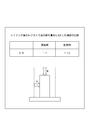
図13は、レジストトリミング後の縦横比の変化量の測定結果図である。
レジストトリミング後の横方向の変化量をA、縦方向の変化量をBとした。
図13に示すように、本実施例のラジカルを用いたレジストトリミング方法では縦横比がA:B=1:1であるのに対して、従来法では縦横比がA:B=1:1.5であった。
従来法ではイオン衝撃等のためにトリミングの縦横比が異方的になり易いが、本実施例のレジストトリミング方法によって、イオン衝撃を減らし、縦横比を等方的にトリミングすることができた。
以上、本発明の好ましい実施形態を添付図面の参照により説明したが、本発明はかかる実施形態に限定されるものではなく、請求の範囲の記載から把握される技術的範囲において種々な形態に変更可能である。
本願は、2008年7月24日提出の日本国特許出願特願2008-190778を基礎として優先権を主張するものであり、その記載内容の全てを、ここに援用する。
Claims (6)
- 反応ガスのプラズマを生成するプラズマ生成工程と、
生成したプラズマからイオン及び電子を除去し、ラジカルを選択的に取り出す除去工程と、
前記イオン及び電子が除去されたプラズマをレジストパターンに照射することで、レジストパターンをトリミングするトリミング工程と、を含むことを特徴とするレジストトリミング方法。 - 前記レジストトリミング方法は、高周波電極が配置されたプラズマ生成空間と、レジストパターンを形成した被処理体を配置可能なトリミング処理空間と、前記プラズマ生成空間と前記トリミング処理空間との間に配され、かつ、両空間を連通する複数の貫通孔を有する導電性部材と、を備えたトリミング装置を用いて実行され、
前記トリミング工程は、前記プラズマ生成空間に反応ガスを導入し、高周波電極に高周波電力を供給し、高周波放電させることで、プラズマを生成し、生成したプラズマを前記導電性部材を介して前記トリミング処理空間に導入することで、イオン及び電子が除去されたプラズマを照射することを特徴とする請求項1に記載のレジストトリミング方法。 - 前記トリミング工程は、電子密度が1×10+7cm-3以下のプラズマを照射することを特徴とする請求項1又は2に記載のレジストトリミング方法。
- 高周波電極が配置されたプラズマ生成空間と、トリミング処理空間と、前記プラズマ生成空間と前記トリミング処理空間との間に配され、かつ、両空間を連通する複数の貫通孔を有する導電性部材と、
前記プラズマ生成空間に反応ガスを導入するガス導入手段と、
前記プラズマ生成空間及びトリミング処理空間を排気する排気手段と、
前記高周波電極への電力供給を行う高周波電力供給手段と、
前記ガス導入手段、前記排気手段及び前記高周波電力供給手段を制御することで、イオン及び電子が除去されたプラズマを前記トリミング処理空間に導入し、当該トリミング処理空間に導入されたレジストパターンをトリミングするトリミング処理を実行するコントローラと、を備えたことを特徴とするトリミング装置。 - 前記コントローラは、レジストパターンが所定のサイズにトリミングされた際に、トリミング処理を終了させるタイマ処理部を有することを特徴とする請求項4に記載のトリミング装置。
- 前記コントローラは、
トリミング速度に関するトリミング速度情報を記憶するトリミング速度情報記憶部と、
前記トリミング速度情報に基づいて、トリミング処理の終了タイミングを決定する終了タイミング演算部と、を有することを特徴とする請求項5に記載のトリミング装置。
Applications Claiming Priority (2)
| Application Number | Priority Date | Filing Date | Title |
|---|---|---|---|
| JP2008-190778 | 2008-07-24 | ||
| JP2008190778A JP2011253832A (ja) | 2008-07-24 | 2008-07-24 | レジストトリミング方法及びトリミング装置 |
Publications (1)
| Publication Number | Publication Date |
|---|---|
| WO2010010706A1 true WO2010010706A1 (ja) | 2010-01-28 |
Family
ID=41570175
Family Applications (1)
| Application Number | Title | Priority Date | Filing Date |
|---|---|---|---|
| PCT/JP2009/003463 Ceased WO2010010706A1 (ja) | 2008-07-24 | 2009-07-23 | レジストトリミング方法及びトリミング装置 |
Country Status (2)
| Country | Link |
|---|---|
| JP (1) | JP2011253832A (ja) |
| WO (1) | WO2010010706A1 (ja) |
Cited By (97)
| Publication number | Priority date | Publication date | Assignee | Title |
|---|---|---|---|---|
| JP2014508424A (ja) * | 2011-03-14 | 2014-04-03 | アプライド マテリアルズ インコーポレイテッド | SiN膜のエッチング方法 |
| US9576809B2 (en) | 2013-11-04 | 2017-02-21 | Applied Materials, Inc. | Etch suppression with germanium |
| US9613822B2 (en) | 2014-09-25 | 2017-04-04 | Applied Materials, Inc. | Oxide etch selectivity enhancement |
| US9659753B2 (en) | 2014-08-07 | 2017-05-23 | Applied Materials, Inc. | Grooved insulator to reduce leakage current |
| US9691645B2 (en) | 2015-08-06 | 2017-06-27 | Applied Materials, Inc. | Bolted wafer chuck thermal management systems and methods for wafer processing systems |
| US9704723B2 (en) | 2013-03-15 | 2017-07-11 | Applied Materials, Inc. | Processing systems and methods for halide scavenging |
| US9711366B2 (en) | 2013-11-12 | 2017-07-18 | Applied Materials, Inc. | Selective etch for metal-containing materials |
| US9721789B1 (en) | 2016-10-04 | 2017-08-01 | Applied Materials, Inc. | Saving ion-damaged spacers |
| US9728437B2 (en) | 2015-02-03 | 2017-08-08 | Applied Materials, Inc. | High temperature chuck for plasma processing systems |
| US9741593B2 (en) | 2015-08-06 | 2017-08-22 | Applied Materials, Inc. | Thermal management systems and methods for wafer processing systems |
| US9754800B2 (en) | 2010-05-27 | 2017-09-05 | Applied Materials, Inc. | Selective etch for silicon films |
| US9768034B1 (en) | 2016-11-11 | 2017-09-19 | Applied Materials, Inc. | Removal methods for high aspect ratio structures |
| US9773695B2 (en) | 2014-07-31 | 2017-09-26 | Applied Materials, Inc. | Integrated bit-line airgap formation and gate stack post clean |
| US9773648B2 (en) | 2013-08-30 | 2017-09-26 | Applied Materials, Inc. | Dual discharge modes operation for remote plasma |
| US9837249B2 (en) | 2014-03-20 | 2017-12-05 | Applied Materials, Inc. | Radial waveguide systems and methods for post-match control of microwaves |
| US9865484B1 (en) | 2016-06-29 | 2018-01-09 | Applied Materials, Inc. | Selective etch using material modification and RF pulsing |
| US9881805B2 (en) | 2015-03-02 | 2018-01-30 | Applied Materials, Inc. | Silicon selective removal |
| US9885117B2 (en) | 2014-03-31 | 2018-02-06 | Applied Materials, Inc. | Conditioned semiconductor system parts |
| US9934942B1 (en) | 2016-10-04 | 2018-04-03 | Applied Materials, Inc. | Chamber with flow-through source |
| US9947549B1 (en) | 2016-10-10 | 2018-04-17 | Applied Materials, Inc. | Cobalt-containing material removal |
| US9966240B2 (en) | 2014-10-14 | 2018-05-08 | Applied Materials, Inc. | Systems and methods for internal surface conditioning assessment in plasma processing equipment |
| US9978564B2 (en) | 2012-09-21 | 2018-05-22 | Applied Materials, Inc. | Chemical control features in wafer process equipment |
| US10026621B2 (en) | 2016-11-14 | 2018-07-17 | Applied Materials, Inc. | SiN spacer profile patterning |
| US10032606B2 (en) | 2012-08-02 | 2018-07-24 | Applied Materials, Inc. | Semiconductor processing with DC assisted RF power for improved control |
| US10043684B1 (en) | 2017-02-06 | 2018-08-07 | Applied Materials, Inc. | Self-limiting atomic thermal etching systems and methods |
| US10043674B1 (en) | 2017-08-04 | 2018-08-07 | Applied Materials, Inc. | Germanium etching systems and methods |
| US10049891B1 (en) | 2017-05-31 | 2018-08-14 | Applied Materials, Inc. | Selective in situ cobalt residue removal |
| US10062579B2 (en) | 2016-10-07 | 2018-08-28 | Applied Materials, Inc. | Selective SiN lateral recess |
| US10062587B2 (en) | 2012-07-18 | 2018-08-28 | Applied Materials, Inc. | Pedestal with multi-zone temperature control and multiple purge capabilities |
| US10062585B2 (en) | 2016-10-04 | 2018-08-28 | Applied Materials, Inc. | Oxygen compatible plasma source |
| US10062575B2 (en) | 2016-09-09 | 2018-08-28 | Applied Materials, Inc. | Poly directional etch by oxidation |
| US10062578B2 (en) | 2011-03-14 | 2018-08-28 | Applied Materials, Inc. | Methods for etch of metal and metal-oxide films |
| US10128086B1 (en) | 2017-10-24 | 2018-11-13 | Applied Materials, Inc. | Silicon pretreatment for nitride removal |
| US10163696B2 (en) | 2016-11-11 | 2018-12-25 | Applied Materials, Inc. | Selective cobalt removal for bottom up gapfill |
| US10170336B1 (en) | 2017-08-04 | 2019-01-01 | Applied Materials, Inc. | Methods for anisotropic control of selective silicon removal |
| US10224210B2 (en) | 2014-12-09 | 2019-03-05 | Applied Materials, Inc. | Plasma processing system with direct outlet toroidal plasma source |
| US10242908B2 (en) | 2016-11-14 | 2019-03-26 | Applied Materials, Inc. | Airgap formation with damage-free copper |
| US10256112B1 (en) | 2017-12-08 | 2019-04-09 | Applied Materials, Inc. | Selective tungsten removal |
| US10256079B2 (en) | 2013-02-08 | 2019-04-09 | Applied Materials, Inc. | Semiconductor processing systems having multiple plasma configurations |
| US10283321B2 (en) | 2011-01-18 | 2019-05-07 | Applied Materials, Inc. | Semiconductor processing system and methods using capacitively coupled plasma |
| US10283324B1 (en) | 2017-10-24 | 2019-05-07 | Applied Materials, Inc. | Oxygen treatment for nitride etching |
| US10297458B2 (en) | 2017-08-07 | 2019-05-21 | Applied Materials, Inc. | Process window widening using coated parts in plasma etch processes |
| US10319649B2 (en) | 2017-04-11 | 2019-06-11 | Applied Materials, Inc. | Optical emission spectroscopy (OES) for remote plasma monitoring |
| US10319739B2 (en) | 2017-02-08 | 2019-06-11 | Applied Materials, Inc. | Accommodating imperfectly aligned memory holes |
| US10319600B1 (en) | 2018-03-12 | 2019-06-11 | Applied Materials, Inc. | Thermal silicon etch |
| US10354889B2 (en) | 2017-07-17 | 2019-07-16 | Applied Materials, Inc. | Non-halogen etching of silicon-containing materials |
| JP2019145761A (ja) * | 2018-02-20 | 2019-08-29 | エーエスエム アイピー ホールディング ビー.ブイ. | 基板処理方法及び装置 |
| US10403507B2 (en) | 2017-02-03 | 2019-09-03 | Applied Materials, Inc. | Shaped etch profile with oxidation |
| US10424485B2 (en) | 2013-03-01 | 2019-09-24 | Applied Materials, Inc. | Enhanced etching processes using remote plasma sources |
| US10424463B2 (en) | 2015-08-07 | 2019-09-24 | Applied Materials, Inc. | Oxide etch selectivity systems and methods |
| US10431429B2 (en) | 2017-02-03 | 2019-10-01 | Applied Materials, Inc. | Systems and methods for radial and azimuthal control of plasma uniformity |
| US10468267B2 (en) | 2017-05-31 | 2019-11-05 | Applied Materials, Inc. | Water-free etching methods |
| US10465294B2 (en) | 2014-05-28 | 2019-11-05 | Applied Materials, Inc. | Oxide and metal removal |
| US10490406B2 (en) | 2018-04-10 | 2019-11-26 | Appled Materials, Inc. | Systems and methods for material breakthrough |
| US10497573B2 (en) | 2018-03-13 | 2019-12-03 | Applied Materials, Inc. | Selective atomic layer etching of semiconductor materials |
| US10504754B2 (en) | 2016-05-19 | 2019-12-10 | Applied Materials, Inc. | Systems and methods for improved semiconductor etching and component protection |
| US10504700B2 (en) | 2015-08-27 | 2019-12-10 | Applied Materials, Inc. | Plasma etching systems and methods with secondary plasma injection |
| US10522371B2 (en) | 2016-05-19 | 2019-12-31 | Applied Materials, Inc. | Systems and methods for improved semiconductor etching and component protection |
| US10541246B2 (en) | 2017-06-26 | 2020-01-21 | Applied Materials, Inc. | 3D flash memory cells which discourage cross-cell electrical tunneling |
| US10541184B2 (en) | 2017-07-11 | 2020-01-21 | Applied Materials, Inc. | Optical emission spectroscopic techniques for monitoring etching |
| US10546729B2 (en) | 2016-10-04 | 2020-01-28 | Applied Materials, Inc. | Dual-channel showerhead with improved profile |
| US10566206B2 (en) | 2016-12-27 | 2020-02-18 | Applied Materials, Inc. | Systems and methods for anisotropic material breakthrough |
| US10573527B2 (en) | 2018-04-06 | 2020-02-25 | Applied Materials, Inc. | Gas-phase selective etching systems and methods |
| US10573496B2 (en) | 2014-12-09 | 2020-02-25 | Applied Materials, Inc. | Direct outlet toroidal plasma source |
| US10593560B2 (en) | 2018-03-01 | 2020-03-17 | Applied Materials, Inc. | Magnetic induction plasma source for semiconductor processes and equipment |
| US10593523B2 (en) | 2014-10-14 | 2020-03-17 | Applied Materials, Inc. | Systems and methods for internal surface conditioning in plasma processing equipment |
| CN110928149A (zh) * | 2018-09-20 | 2020-03-27 | 长鑫存储技术有限公司 | 关键尺寸的控制方法及控制系统 |
| US10615047B2 (en) | 2018-02-28 | 2020-04-07 | Applied Materials, Inc. | Systems and methods to form airgaps |
| US10629473B2 (en) | 2016-09-09 | 2020-04-21 | Applied Materials, Inc. | Footing removal for nitride spacer |
| US10672642B2 (en) | 2018-07-24 | 2020-06-02 | Applied Materials, Inc. | Systems and methods for pedestal configuration |
| US10679870B2 (en) | 2018-02-15 | 2020-06-09 | Applied Materials, Inc. | Semiconductor processing chamber multistage mixing apparatus |
| US10699879B2 (en) | 2018-04-17 | 2020-06-30 | Applied Materials, Inc. | Two piece electrode assembly with gap for plasma control |
| US10727080B2 (en) | 2017-07-07 | 2020-07-28 | Applied Materials, Inc. | Tantalum-containing material removal |
| US10755941B2 (en) | 2018-07-06 | 2020-08-25 | Applied Materials, Inc. | Self-limiting selective etching systems and methods |
| US10854426B2 (en) | 2018-01-08 | 2020-12-01 | Applied Materials, Inc. | Metal recess for semiconductor structures |
| US10872778B2 (en) | 2018-07-06 | 2020-12-22 | Applied Materials, Inc. | Systems and methods utilizing solid-phase etchants |
| US10886137B2 (en) | 2018-04-30 | 2021-01-05 | Applied Materials, Inc. | Selective nitride removal |
| US10892198B2 (en) | 2018-09-14 | 2021-01-12 | Applied Materials, Inc. | Systems and methods for improved performance in semiconductor processing |
| US10903054B2 (en) | 2017-12-19 | 2021-01-26 | Applied Materials, Inc. | Multi-zone gas distribution systems and methods |
| US10920320B2 (en) | 2017-06-16 | 2021-02-16 | Applied Materials, Inc. | Plasma health determination in semiconductor substrate processing reactors |
| US10920319B2 (en) | 2019-01-11 | 2021-02-16 | Applied Materials, Inc. | Ceramic showerheads with conductive electrodes |
| US10943834B2 (en) | 2017-03-13 | 2021-03-09 | Applied Materials, Inc. | Replacement contact process |
| US10964512B2 (en) | 2018-02-15 | 2021-03-30 | Applied Materials, Inc. | Semiconductor processing chamber multistage mixing apparatus and methods |
| US11049755B2 (en) | 2018-09-14 | 2021-06-29 | Applied Materials, Inc. | Semiconductor substrate supports with embedded RF shield |
| US11062887B2 (en) | 2018-09-17 | 2021-07-13 | Applied Materials, Inc. | High temperature RF heater pedestals |
| US11121002B2 (en) | 2018-10-24 | 2021-09-14 | Applied Materials, Inc. | Systems and methods for etching metals and metal derivatives |
| US11239061B2 (en) | 2014-11-26 | 2022-02-01 | Applied Materials, Inc. | Methods and systems to enhance process uniformity |
| US11257693B2 (en) | 2015-01-09 | 2022-02-22 | Applied Materials, Inc. | Methods and systems to improve pedestal temperature control |
| US11276559B2 (en) | 2017-05-17 | 2022-03-15 | Applied Materials, Inc. | Semiconductor processing chamber for multiple precursor flow |
| US11276590B2 (en) | 2017-05-17 | 2022-03-15 | Applied Materials, Inc. | Multi-zone semiconductor substrate supports |
| US11328909B2 (en) | 2017-12-22 | 2022-05-10 | Applied Materials, Inc. | Chamber conditioning and removal processes |
| US11417534B2 (en) | 2018-09-21 | 2022-08-16 | Applied Materials, Inc. | Selective material removal |
| US11437242B2 (en) | 2018-11-27 | 2022-09-06 | Applied Materials, Inc. | Selective removal of silicon-containing materials |
| US11594428B2 (en) | 2015-02-03 | 2023-02-28 | Applied Materials, Inc. | Low temperature chuck for plasma processing systems |
| US11682560B2 (en) | 2018-10-11 | 2023-06-20 | Applied Materials, Inc. | Systems and methods for hafnium-containing film removal |
| US11721527B2 (en) | 2019-01-07 | 2023-08-08 | Applied Materials, Inc. | Processing chamber mixing systems |
| US12340979B2 (en) | 2017-05-17 | 2025-06-24 | Applied Materials, Inc. | Semiconductor processing chamber for improved precursor flow |
Families Citing this family (2)
| Publication number | Priority date | Publication date | Assignee | Title |
|---|---|---|---|---|
| US9343308B2 (en) * | 2013-10-28 | 2016-05-17 | Asm Ip Holding B.V. | Method for trimming carbon-containing film at reduced trimming rate |
| US10354883B2 (en) * | 2017-10-03 | 2019-07-16 | Mattson Technology, Inc. | Surface treatment of silicon or silicon germanium surfaces using organic radicals |
Citations (8)
| Publication number | Priority date | Publication date | Assignee | Title |
|---|---|---|---|---|
| JPS61267325A (ja) * | 1985-05-22 | 1986-11-26 | Tokyo Denshi Kagaku Kk | 有機膜の除去方法 |
| JPH01192118A (ja) * | 1988-01-28 | 1989-08-02 | Fujitsu Ltd | レジスト膜除去装置 |
| JPH0845906A (ja) * | 1994-07-28 | 1996-02-16 | Sony Corp | パターン形成方法及び該パターン形成方法を用いた半導体装置の製造方法 |
| JP2003086572A (ja) * | 2001-09-13 | 2003-03-20 | Hynix Semiconductor Inc | 半導体装置のビットライン形成方法 |
| JP2003179064A (ja) * | 2001-12-10 | 2003-06-27 | Sony Corp | 配線パターンの形成方法 |
| JP2005026292A (ja) * | 2003-06-30 | 2005-01-27 | Fujitsu Ltd | 半導体装置及びその製造方法、半導体製造装置 |
| JP2005085878A (ja) * | 2003-09-05 | 2005-03-31 | Hitachi Ltd | マスクトリミング装置及びマスクトリミング方法 |
| JP2007081383A (ja) * | 2005-08-15 | 2007-03-29 | Fujitsu Ltd | 微細構造の製造方法 |
-
2008
- 2008-07-24 JP JP2008190778A patent/JP2011253832A/ja not_active Withdrawn
-
2009
- 2009-07-23 WO PCT/JP2009/003463 patent/WO2010010706A1/ja not_active Ceased
Patent Citations (8)
| Publication number | Priority date | Publication date | Assignee | Title |
|---|---|---|---|---|
| JPS61267325A (ja) * | 1985-05-22 | 1986-11-26 | Tokyo Denshi Kagaku Kk | 有機膜の除去方法 |
| JPH01192118A (ja) * | 1988-01-28 | 1989-08-02 | Fujitsu Ltd | レジスト膜除去装置 |
| JPH0845906A (ja) * | 1994-07-28 | 1996-02-16 | Sony Corp | パターン形成方法及び該パターン形成方法を用いた半導体装置の製造方法 |
| JP2003086572A (ja) * | 2001-09-13 | 2003-03-20 | Hynix Semiconductor Inc | 半導体装置のビットライン形成方法 |
| JP2003179064A (ja) * | 2001-12-10 | 2003-06-27 | Sony Corp | 配線パターンの形成方法 |
| JP2005026292A (ja) * | 2003-06-30 | 2005-01-27 | Fujitsu Ltd | 半導体装置及びその製造方法、半導体製造装置 |
| JP2005085878A (ja) * | 2003-09-05 | 2005-03-31 | Hitachi Ltd | マスクトリミング装置及びマスクトリミング方法 |
| JP2007081383A (ja) * | 2005-08-15 | 2007-03-29 | Fujitsu Ltd | 微細構造の製造方法 |
Cited By (139)
| Publication number | Priority date | Publication date | Assignee | Title |
|---|---|---|---|---|
| US9754800B2 (en) | 2010-05-27 | 2017-09-05 | Applied Materials, Inc. | Selective etch for silicon films |
| US10283321B2 (en) | 2011-01-18 | 2019-05-07 | Applied Materials, Inc. | Semiconductor processing system and methods using capacitively coupled plasma |
| KR101903751B1 (ko) * | 2011-03-14 | 2018-10-04 | 어플라이드 머티어리얼스, 인코포레이티드 | Sin 필름들의 에칭을 위한 방법들 |
| US10062578B2 (en) | 2011-03-14 | 2018-08-28 | Applied Materials, Inc. | Methods for etch of metal and metal-oxide films |
| US9842744B2 (en) | 2011-03-14 | 2017-12-12 | Applied Materials, Inc. | Methods for etch of SiN films |
| JP2014508424A (ja) * | 2011-03-14 | 2014-04-03 | アプライド マテリアルズ インコーポレイテッド | SiN膜のエッチング方法 |
| US10062587B2 (en) | 2012-07-18 | 2018-08-28 | Applied Materials, Inc. | Pedestal with multi-zone temperature control and multiple purge capabilities |
| US10032606B2 (en) | 2012-08-02 | 2018-07-24 | Applied Materials, Inc. | Semiconductor processing with DC assisted RF power for improved control |
| US9978564B2 (en) | 2012-09-21 | 2018-05-22 | Applied Materials, Inc. | Chemical control features in wafer process equipment |
| US11264213B2 (en) | 2012-09-21 | 2022-03-01 | Applied Materials, Inc. | Chemical control features in wafer process equipment |
| US10354843B2 (en) | 2012-09-21 | 2019-07-16 | Applied Materials, Inc. | Chemical control features in wafer process equipment |
| US10256079B2 (en) | 2013-02-08 | 2019-04-09 | Applied Materials, Inc. | Semiconductor processing systems having multiple plasma configurations |
| US11024486B2 (en) | 2013-02-08 | 2021-06-01 | Applied Materials, Inc. | Semiconductor processing systems having multiple plasma configurations |
| US10424485B2 (en) | 2013-03-01 | 2019-09-24 | Applied Materials, Inc. | Enhanced etching processes using remote plasma sources |
| US9704723B2 (en) | 2013-03-15 | 2017-07-11 | Applied Materials, Inc. | Processing systems and methods for halide scavenging |
| US9773648B2 (en) | 2013-08-30 | 2017-09-26 | Applied Materials, Inc. | Dual discharge modes operation for remote plasma |
| US9576809B2 (en) | 2013-11-04 | 2017-02-21 | Applied Materials, Inc. | Etch suppression with germanium |
| US9711366B2 (en) | 2013-11-12 | 2017-07-18 | Applied Materials, Inc. | Selective etch for metal-containing materials |
| US9837249B2 (en) | 2014-03-20 | 2017-12-05 | Applied Materials, Inc. | Radial waveguide systems and methods for post-match control of microwaves |
| US9885117B2 (en) | 2014-03-31 | 2018-02-06 | Applied Materials, Inc. | Conditioned semiconductor system parts |
| US9903020B2 (en) | 2014-03-31 | 2018-02-27 | Applied Materials, Inc. | Generation of compact alumina passivation layers on aluminum plasma equipment components |
| US10465294B2 (en) | 2014-05-28 | 2019-11-05 | Applied Materials, Inc. | Oxide and metal removal |
| US9773695B2 (en) | 2014-07-31 | 2017-09-26 | Applied Materials, Inc. | Integrated bit-line airgap formation and gate stack post clean |
| US9659753B2 (en) | 2014-08-07 | 2017-05-23 | Applied Materials, Inc. | Grooved insulator to reduce leakage current |
| US9837284B2 (en) | 2014-09-25 | 2017-12-05 | Applied Materials, Inc. | Oxide etch selectivity enhancement |
| US9613822B2 (en) | 2014-09-25 | 2017-04-04 | Applied Materials, Inc. | Oxide etch selectivity enhancement |
| US9966240B2 (en) | 2014-10-14 | 2018-05-08 | Applied Materials, Inc. | Systems and methods for internal surface conditioning assessment in plasma processing equipment |
| US10796922B2 (en) | 2014-10-14 | 2020-10-06 | Applied Materials, Inc. | Systems and methods for internal surface conditioning assessment in plasma processing equipment |
| US10490418B2 (en) | 2014-10-14 | 2019-11-26 | Applied Materials, Inc. | Systems and methods for internal surface conditioning assessment in plasma processing equipment |
| US10707061B2 (en) | 2014-10-14 | 2020-07-07 | Applied Materials, Inc. | Systems and methods for internal surface conditioning in plasma processing equipment |
| US10593523B2 (en) | 2014-10-14 | 2020-03-17 | Applied Materials, Inc. | Systems and methods for internal surface conditioning in plasma processing equipment |
| US11239061B2 (en) | 2014-11-26 | 2022-02-01 | Applied Materials, Inc. | Methods and systems to enhance process uniformity |
| US11637002B2 (en) | 2014-11-26 | 2023-04-25 | Applied Materials, Inc. | Methods and systems to enhance process uniformity |
| US10573496B2 (en) | 2014-12-09 | 2020-02-25 | Applied Materials, Inc. | Direct outlet toroidal plasma source |
| US10224210B2 (en) | 2014-12-09 | 2019-03-05 | Applied Materials, Inc. | Plasma processing system with direct outlet toroidal plasma source |
| US11257693B2 (en) | 2015-01-09 | 2022-02-22 | Applied Materials, Inc. | Methods and systems to improve pedestal temperature control |
| US10468285B2 (en) | 2015-02-03 | 2019-11-05 | Applied Materials, Inc. | High temperature chuck for plasma processing systems |
| US9728437B2 (en) | 2015-02-03 | 2017-08-08 | Applied Materials, Inc. | High temperature chuck for plasma processing systems |
| US11594428B2 (en) | 2015-02-03 | 2023-02-28 | Applied Materials, Inc. | Low temperature chuck for plasma processing systems |
| US12009228B2 (en) | 2015-02-03 | 2024-06-11 | Applied Materials, Inc. | Low temperature chuck for plasma processing systems |
| US9881805B2 (en) | 2015-03-02 | 2018-01-30 | Applied Materials, Inc. | Silicon selective removal |
| US10147620B2 (en) | 2015-08-06 | 2018-12-04 | Applied Materials, Inc. | Bolted wafer chuck thermal management systems and methods for wafer processing systems |
| US10468276B2 (en) | 2015-08-06 | 2019-11-05 | Applied Materials, Inc. | Thermal management systems and methods for wafer processing systems |
| US9741593B2 (en) | 2015-08-06 | 2017-08-22 | Applied Materials, Inc. | Thermal management systems and methods for wafer processing systems |
| US11158527B2 (en) | 2015-08-06 | 2021-10-26 | Applied Materials, Inc. | Thermal management systems and methods for wafer processing systems |
| US10607867B2 (en) | 2015-08-06 | 2020-03-31 | Applied Materials, Inc. | Bolted wafer chuck thermal management systems and methods for wafer processing systems |
| US9691645B2 (en) | 2015-08-06 | 2017-06-27 | Applied Materials, Inc. | Bolted wafer chuck thermal management systems and methods for wafer processing systems |
| US10424464B2 (en) | 2015-08-07 | 2019-09-24 | Applied Materials, Inc. | Oxide etch selectivity systems and methods |
| US10424463B2 (en) | 2015-08-07 | 2019-09-24 | Applied Materials, Inc. | Oxide etch selectivity systems and methods |
| US11476093B2 (en) | 2015-08-27 | 2022-10-18 | Applied Materials, Inc. | Plasma etching systems and methods with secondary plasma injection |
| US10504700B2 (en) | 2015-08-27 | 2019-12-10 | Applied Materials, Inc. | Plasma etching systems and methods with secondary plasma injection |
| US11735441B2 (en) | 2016-05-19 | 2023-08-22 | Applied Materials, Inc. | Systems and methods for improved semiconductor etching and component protection |
| US10504754B2 (en) | 2016-05-19 | 2019-12-10 | Applied Materials, Inc. | Systems and methods for improved semiconductor etching and component protection |
| US10522371B2 (en) | 2016-05-19 | 2019-12-31 | Applied Materials, Inc. | Systems and methods for improved semiconductor etching and component protection |
| US12057329B2 (en) | 2016-06-29 | 2024-08-06 | Applied Materials, Inc. | Selective etch using material modification and RF pulsing |
| US9865484B1 (en) | 2016-06-29 | 2018-01-09 | Applied Materials, Inc. | Selective etch using material modification and RF pulsing |
| US10629473B2 (en) | 2016-09-09 | 2020-04-21 | Applied Materials, Inc. | Footing removal for nitride spacer |
| US10062575B2 (en) | 2016-09-09 | 2018-08-28 | Applied Materials, Inc. | Poly directional etch by oxidation |
| US10541113B2 (en) | 2016-10-04 | 2020-01-21 | Applied Materials, Inc. | Chamber with flow-through source |
| US10546729B2 (en) | 2016-10-04 | 2020-01-28 | Applied Materials, Inc. | Dual-channel showerhead with improved profile |
| US10224180B2 (en) | 2016-10-04 | 2019-03-05 | Applied Materials, Inc. | Chamber with flow-through source |
| US10062585B2 (en) | 2016-10-04 | 2018-08-28 | Applied Materials, Inc. | Oxygen compatible plasma source |
| US11049698B2 (en) | 2016-10-04 | 2021-06-29 | Applied Materials, Inc. | Dual-channel showerhead with improved profile |
| US9934942B1 (en) | 2016-10-04 | 2018-04-03 | Applied Materials, Inc. | Chamber with flow-through source |
| US9721789B1 (en) | 2016-10-04 | 2017-08-01 | Applied Materials, Inc. | Saving ion-damaged spacers |
| US10062579B2 (en) | 2016-10-07 | 2018-08-28 | Applied Materials, Inc. | Selective SiN lateral recess |
| US10319603B2 (en) | 2016-10-07 | 2019-06-11 | Applied Materials, Inc. | Selective SiN lateral recess |
| US9947549B1 (en) | 2016-10-10 | 2018-04-17 | Applied Materials, Inc. | Cobalt-containing material removal |
| US10163696B2 (en) | 2016-11-11 | 2018-12-25 | Applied Materials, Inc. | Selective cobalt removal for bottom up gapfill |
| US9768034B1 (en) | 2016-11-11 | 2017-09-19 | Applied Materials, Inc. | Removal methods for high aspect ratio structures |
| US10186428B2 (en) | 2016-11-11 | 2019-01-22 | Applied Materials, Inc. | Removal methods for high aspect ratio structures |
| US10770346B2 (en) | 2016-11-11 | 2020-09-08 | Applied Materials, Inc. | Selective cobalt removal for bottom up gapfill |
| US10600639B2 (en) | 2016-11-14 | 2020-03-24 | Applied Materials, Inc. | SiN spacer profile patterning |
| US10026621B2 (en) | 2016-11-14 | 2018-07-17 | Applied Materials, Inc. | SiN spacer profile patterning |
| US10242908B2 (en) | 2016-11-14 | 2019-03-26 | Applied Materials, Inc. | Airgap formation with damage-free copper |
| US10566206B2 (en) | 2016-12-27 | 2020-02-18 | Applied Materials, Inc. | Systems and methods for anisotropic material breakthrough |
| US10403507B2 (en) | 2017-02-03 | 2019-09-03 | Applied Materials, Inc. | Shaped etch profile with oxidation |
| US10903052B2 (en) | 2017-02-03 | 2021-01-26 | Applied Materials, Inc. | Systems and methods for radial and azimuthal control of plasma uniformity |
| US10431429B2 (en) | 2017-02-03 | 2019-10-01 | Applied Materials, Inc. | Systems and methods for radial and azimuthal control of plasma uniformity |
| US10043684B1 (en) | 2017-02-06 | 2018-08-07 | Applied Materials, Inc. | Self-limiting atomic thermal etching systems and methods |
| US10325923B2 (en) | 2017-02-08 | 2019-06-18 | Applied Materials, Inc. | Accommodating imperfectly aligned memory holes |
| US10319739B2 (en) | 2017-02-08 | 2019-06-11 | Applied Materials, Inc. | Accommodating imperfectly aligned memory holes |
| US10529737B2 (en) | 2017-02-08 | 2020-01-07 | Applied Materials, Inc. | Accommodating imperfectly aligned memory holes |
| US10943834B2 (en) | 2017-03-13 | 2021-03-09 | Applied Materials, Inc. | Replacement contact process |
| US10319649B2 (en) | 2017-04-11 | 2019-06-11 | Applied Materials, Inc. | Optical emission spectroscopy (OES) for remote plasma monitoring |
| US11915950B2 (en) | 2017-05-17 | 2024-02-27 | Applied Materials, Inc. | Multi-zone semiconductor substrate supports |
| US12340979B2 (en) | 2017-05-17 | 2025-06-24 | Applied Materials, Inc. | Semiconductor processing chamber for improved precursor flow |
| US11276590B2 (en) | 2017-05-17 | 2022-03-15 | Applied Materials, Inc. | Multi-zone semiconductor substrate supports |
| US11361939B2 (en) | 2017-05-17 | 2022-06-14 | Applied Materials, Inc. | Semiconductor processing chamber for multiple precursor flow |
| US11276559B2 (en) | 2017-05-17 | 2022-03-15 | Applied Materials, Inc. | Semiconductor processing chamber for multiple precursor flow |
| US10497579B2 (en) | 2017-05-31 | 2019-12-03 | Applied Materials, Inc. | Water-free etching methods |
| US10049891B1 (en) | 2017-05-31 | 2018-08-14 | Applied Materials, Inc. | Selective in situ cobalt residue removal |
| US10468267B2 (en) | 2017-05-31 | 2019-11-05 | Applied Materials, Inc. | Water-free etching methods |
| US10920320B2 (en) | 2017-06-16 | 2021-02-16 | Applied Materials, Inc. | Plasma health determination in semiconductor substrate processing reactors |
| US10541246B2 (en) | 2017-06-26 | 2020-01-21 | Applied Materials, Inc. | 3D flash memory cells which discourage cross-cell electrical tunneling |
| US10727080B2 (en) | 2017-07-07 | 2020-07-28 | Applied Materials, Inc. | Tantalum-containing material removal |
| US10541184B2 (en) | 2017-07-11 | 2020-01-21 | Applied Materials, Inc. | Optical emission spectroscopic techniques for monitoring etching |
| US10354889B2 (en) | 2017-07-17 | 2019-07-16 | Applied Materials, Inc. | Non-halogen etching of silicon-containing materials |
| US10170336B1 (en) | 2017-08-04 | 2019-01-01 | Applied Materials, Inc. | Methods for anisotropic control of selective silicon removal |
| US10043674B1 (en) | 2017-08-04 | 2018-08-07 | Applied Materials, Inc. | Germanium etching systems and methods |
| US10593553B2 (en) | 2017-08-04 | 2020-03-17 | Applied Materials, Inc. | Germanium etching systems and methods |
| US11101136B2 (en) | 2017-08-07 | 2021-08-24 | Applied Materials, Inc. | Process window widening using coated parts in plasma etch processes |
| US10297458B2 (en) | 2017-08-07 | 2019-05-21 | Applied Materials, Inc. | Process window widening using coated parts in plasma etch processes |
| US10128086B1 (en) | 2017-10-24 | 2018-11-13 | Applied Materials, Inc. | Silicon pretreatment for nitride removal |
| US10283324B1 (en) | 2017-10-24 | 2019-05-07 | Applied Materials, Inc. | Oxygen treatment for nitride etching |
| US10256112B1 (en) | 2017-12-08 | 2019-04-09 | Applied Materials, Inc. | Selective tungsten removal |
| US12148597B2 (en) | 2017-12-19 | 2024-11-19 | Applied Materials, Inc. | Multi-zone gas distribution systems and methods |
| US10903054B2 (en) | 2017-12-19 | 2021-01-26 | Applied Materials, Inc. | Multi-zone gas distribution systems and methods |
| US11328909B2 (en) | 2017-12-22 | 2022-05-10 | Applied Materials, Inc. | Chamber conditioning and removal processes |
| US10854426B2 (en) | 2018-01-08 | 2020-12-01 | Applied Materials, Inc. | Metal recess for semiconductor structures |
| US10861676B2 (en) | 2018-01-08 | 2020-12-08 | Applied Materials, Inc. | Metal recess for semiconductor structures |
| US10964512B2 (en) | 2018-02-15 | 2021-03-30 | Applied Materials, Inc. | Semiconductor processing chamber multistage mixing apparatus and methods |
| US10679870B2 (en) | 2018-02-15 | 2020-06-09 | Applied Materials, Inc. | Semiconductor processing chamber multistage mixing apparatus |
| US10699921B2 (en) | 2018-02-15 | 2020-06-30 | Applied Materials, Inc. | Semiconductor processing chamber multistage mixing apparatus |
| JP7250442B2 (ja) | 2018-02-20 | 2023-04-03 | エーエスエム アイピー ホールディング ビー.ブイ. | 基板処理方法及び装置 |
| JP2019145761A (ja) * | 2018-02-20 | 2019-08-29 | エーエスエム アイピー ホールディング ビー.ブイ. | 基板処理方法及び装置 |
| US10615047B2 (en) | 2018-02-28 | 2020-04-07 | Applied Materials, Inc. | Systems and methods to form airgaps |
| US10593560B2 (en) | 2018-03-01 | 2020-03-17 | Applied Materials, Inc. | Magnetic induction plasma source for semiconductor processes and equipment |
| US10319600B1 (en) | 2018-03-12 | 2019-06-11 | Applied Materials, Inc. | Thermal silicon etch |
| US11004689B2 (en) | 2018-03-12 | 2021-05-11 | Applied Materials, Inc. | Thermal silicon etch |
| US10497573B2 (en) | 2018-03-13 | 2019-12-03 | Applied Materials, Inc. | Selective atomic layer etching of semiconductor materials |
| US10573527B2 (en) | 2018-04-06 | 2020-02-25 | Applied Materials, Inc. | Gas-phase selective etching systems and methods |
| US10490406B2 (en) | 2018-04-10 | 2019-11-26 | Appled Materials, Inc. | Systems and methods for material breakthrough |
| US10699879B2 (en) | 2018-04-17 | 2020-06-30 | Applied Materials, Inc. | Two piece electrode assembly with gap for plasma control |
| US10886137B2 (en) | 2018-04-30 | 2021-01-05 | Applied Materials, Inc. | Selective nitride removal |
| US10872778B2 (en) | 2018-07-06 | 2020-12-22 | Applied Materials, Inc. | Systems and methods utilizing solid-phase etchants |
| US10755941B2 (en) | 2018-07-06 | 2020-08-25 | Applied Materials, Inc. | Self-limiting selective etching systems and methods |
| US10672642B2 (en) | 2018-07-24 | 2020-06-02 | Applied Materials, Inc. | Systems and methods for pedestal configuration |
| US10892198B2 (en) | 2018-09-14 | 2021-01-12 | Applied Materials, Inc. | Systems and methods for improved performance in semiconductor processing |
| US11049755B2 (en) | 2018-09-14 | 2021-06-29 | Applied Materials, Inc. | Semiconductor substrate supports with embedded RF shield |
| US11062887B2 (en) | 2018-09-17 | 2021-07-13 | Applied Materials, Inc. | High temperature RF heater pedestals |
| CN110928149B (zh) * | 2018-09-20 | 2024-04-19 | 长鑫存储技术有限公司 | 关键尺寸的控制方法及控制系统 |
| CN110928149A (zh) * | 2018-09-20 | 2020-03-27 | 长鑫存储技术有限公司 | 关键尺寸的控制方法及控制系统 |
| US11417534B2 (en) | 2018-09-21 | 2022-08-16 | Applied Materials, Inc. | Selective material removal |
| US11682560B2 (en) | 2018-10-11 | 2023-06-20 | Applied Materials, Inc. | Systems and methods for hafnium-containing film removal |
| US11121002B2 (en) | 2018-10-24 | 2021-09-14 | Applied Materials, Inc. | Systems and methods for etching metals and metal derivatives |
| US11437242B2 (en) | 2018-11-27 | 2022-09-06 | Applied Materials, Inc. | Selective removal of silicon-containing materials |
| US11721527B2 (en) | 2019-01-07 | 2023-08-08 | Applied Materials, Inc. | Processing chamber mixing systems |
| US10920319B2 (en) | 2019-01-11 | 2021-02-16 | Applied Materials, Inc. | Ceramic showerheads with conductive electrodes |
Also Published As
| Publication number | Publication date |
|---|---|
| JP2011253832A (ja) | 2011-12-15 |
Similar Documents
| Publication | Publication Date | Title |
|---|---|---|
| WO2010010706A1 (ja) | レジストトリミング方法及びトリミング装置 | |
| TWI757334B (zh) | 準原子層蝕刻方法 | |
| US8329585B2 (en) | Method for reducing line width roughness with plasma pre-etch treatment on photoresist | |
| KR101455883B1 (ko) | 펄스화된 초고 애스펙트비 유전체 식각 | |
| TWI423322B (zh) | 利用氫變化之光阻調整 | |
| CN101606231B (zh) | 超高纵横比电介质刻蚀 | |
| KR100976882B1 (ko) | 반도체 장치의 제조 방법 및 기억 매체 | |
| US10975468B2 (en) | Method of cleaning plasma processing apparatus | |
| US9911607B2 (en) | Method of processing target object | |
| TWI748360B (zh) | 電漿處理方法及電漿處理裝置 | |
| TWI413187B (zh) | Method for forming amorphous carbon film, amorphous carbon film, multilayer resist film, manufacturing method of semiconductor device, and computer readable recording medium | |
| US7491343B2 (en) | Line end shortening reduction during etch | |
| US8207066B2 (en) | Dry etching method | |
| JP5486883B2 (ja) | 被処理体の処理方法 | |
| JP2004022747A (ja) | エッチング処理装置及び処理方法 | |
| JP5064319B2 (ja) | プラズマエッチング方法、制御プログラム及びコンピュータ記憶媒体 | |
| CN102365392A (zh) | 等离子体蚀刻方法 | |
| US8709952B2 (en) | Etching method, etching apparatus, and computer-readable recording medium | |
| TW201841089A (zh) | 檢查流量控制器之方法及處理被處理體之方法 | |
| Rudenko et al. | Plasma etching of poly-Si/SiO2/Si structures: Langmuir-probe and optical-emission-spectroscopy monitoring | |
| KR20070045082A (ko) | 드라이에칭방법 | |
| US12237174B2 (en) | Etching method | |
| TW573326B (en) | Storage poly process without carbon contamination | |
| JP2010062212A (ja) | 半導体装置の製造方法 | |
| US7407597B2 (en) | Line end shortening reduction during etch |
Legal Events
| Date | Code | Title | Description |
|---|---|---|---|
| 121 | Ep: the epo has been informed by wipo that ep was designated in this application |
Ref document number: 09800222 Country of ref document: EP Kind code of ref document: A1 |
|
| DPE1 | Request for preliminary examination filed after expiration of 19th month from priority date (pct application filed from 20040101) | ||
| NENP | Non-entry into the national phase |
Ref country code: DE |
|
| 122 | Ep: pct application non-entry in european phase |
Ref document number: 09800222 Country of ref document: EP Kind code of ref document: A1 |
|
| NENP | Non-entry into the national phase |
Ref country code: JP |