WO2010016331A1 - デバイスの製造方法 - Google Patents
デバイスの製造方法 Download PDFInfo
- Publication number
- WO2010016331A1 WO2010016331A1 PCT/JP2009/060825 JP2009060825W WO2010016331A1 WO 2010016331 A1 WO2010016331 A1 WO 2010016331A1 JP 2009060825 W JP2009060825 W JP 2009060825W WO 2010016331 A1 WO2010016331 A1 WO 2010016331A1
- Authority
- WO
- WIPO (PCT)
- Prior art keywords
- light
- layer
- transfer
- substrate
- organic
- Prior art date
- Legal status (The legal status is an assumption and is not a legal conclusion. Google has not performed a legal analysis and makes no representation as to the accuracy of the status listed.)
- Ceased
Links
Images


Classifications
-
- H—ELECTRICITY
- H10—SEMICONDUCTOR DEVICES; ELECTRIC SOLID-STATE DEVICES NOT OTHERWISE PROVIDED FOR
- H10K—ORGANIC ELECTRIC SOLID-STATE DEVICES
- H10K71/00—Manufacture or treatment specially adapted for the organic devices covered by this subclass
- H10K71/10—Deposition of organic active material
- H10K71/12—Deposition of organic active material using liquid deposition, e.g. spin coating
-
- H—ELECTRICITY
- H10—SEMICONDUCTOR DEVICES; ELECTRIC SOLID-STATE DEVICES NOT OTHERWISE PROVIDED FOR
- H10K—ORGANIC ELECTRIC SOLID-STATE DEVICES
- H10K50/00—Organic light-emitting devices
- H10K50/10—OLEDs or polymer light-emitting diodes [PLED]
- H10K50/11—OLEDs or polymer light-emitting diodes [PLED] characterised by the electroluminescent [EL] layers
-
- H—ELECTRICITY
- H10—SEMICONDUCTOR DEVICES; ELECTRIC SOLID-STATE DEVICES NOT OTHERWISE PROVIDED FOR
- H10K—ORGANIC ELECTRIC SOLID-STATE DEVICES
- H10K71/00—Manufacture or treatment specially adapted for the organic devices covered by this subclass
- H10K71/10—Deposition of organic active material
- H10K71/18—Deposition of organic active material using non-liquid printing techniques, e.g. thermal transfer printing from a donor sheet
-
- H—ELECTRICITY
- H10—SEMICONDUCTOR DEVICES; ELECTRIC SOLID-STATE DEVICES NOT OTHERWISE PROVIDED FOR
- H10K—ORGANIC ELECTRIC SOLID-STATE DEVICES
- H10K71/00—Manufacture or treatment specially adapted for the organic devices covered by this subclass
- H10K71/40—Thermal treatment, e.g. annealing in the presence of a solvent vapour
-
- H—ELECTRICITY
- H10—SEMICONDUCTOR DEVICES; ELECTRIC SOLID-STATE DEVICES NOT OTHERWISE PROVIDED FOR
- H10K—ORGANIC ELECTRIC SOLID-STATE DEVICES
- H10K85/00—Organic materials used in the body or electrodes of devices covered by this subclass
- H10K85/60—Organic compounds having low molecular weight
- H10K85/615—Polycyclic condensed aromatic hydrocarbons, e.g. anthracene
- H10K85/622—Polycyclic condensed aromatic hydrocarbons, e.g. anthracene containing four rings, e.g. pyrene
-
- H—ELECTRICITY
- H10—SEMICONDUCTOR DEVICES; ELECTRIC SOLID-STATE DEVICES NOT OTHERWISE PROVIDED FOR
- H10K—ORGANIC ELECTRIC SOLID-STATE DEVICES
- H10K71/00—Manufacture or treatment specially adapted for the organic devices covered by this subclass
Definitions
- the present invention relates to a method for forming a thin film constituting a device such as an organic EL element, an organic TFT, a photoelectric conversion element, and various sensors, and a method for manufacturing a device using the film forming method.
- Organic devices have a structure in which an organic material is sandwiched between a cathode and an anode.
- organic EL electroluminescence
- organic transistors current control
- photoelectric conversion organic solar cells
- organic device manufacturing methods can be classified into a dry process represented by a vacuum deposition method and a wet process such as a spin coating method and an inkjet method.
- the vacuum evaporation method is a method of forming a film on a device substrate by sublimating a low molecular material in vacuum. According to this method, a device in which a plurality of types of materials are laminated while arbitrarily controlling the film thickness is manufactured. Is possible. Any of the above-described organic EL, organic transistor, and organic solar cell elements can be produced by this method (see Non-Patent Documents 1 to 3). In particular, the organic EL element can provide a practical high-performance element. .
- problems with the vacuum deposition method include that the manufacturing apparatus is expensive, the material utilization rate is low, and it is difficult to produce a large-area device by patterning using a shadow mask.
- the wet process has the advantage that it can solve the problems that were difficult with the vacuum deposition method, such as the ease of manufacturing a large-area device that requires material utilization and patterning (see Non-Patent Document 4).
- the object of the present invention is to provide a method for manufacturing a device that solves such a problem, has the same characteristics of the element as those produced by vapor deposition, and is compatible with an increase in size.
- the present invention provides a coating process for applying a precursor material, which is soluble in a solvent at the time of coating and can be converted into a device constituent material after coating, onto a donor substrate, a conversion process for converting the precursor material into a device constituent material, and the donor. And a transfer step of transferring a material on the substrate to the device substrate.
- the present invention a high-performance organic device equivalent to that produced by the vapor deposition method can be manufactured.
- the present invention is a technique suitable for manufacturing a large organic EL display.
- Sectional drawing which shows an example of the light irradiation method to the donor substrate in this invention.
- Sectional drawing which shows another example of the light irradiation method to the donor substrate in this invention.
- the perspective view which shows an example of the light irradiation method in this invention.
- the perspective view which shows another example of the light irradiation method in this invention.
- Sectional drawing which shows an example of the organic EL element by which the light emitting layer was patterned by this invention.
- Sectional drawing which shows an example of the transcription
- the figure which shows an example of the shape of ITO produced on the glass substrate.
- the manufacturing method of the present invention includes (1) a coating step in which a precursor material that is solvent-soluble at the time of coating and can be converted into a device constituent material after coating is applied to a donor substrate, and (2) the precursor material is converted into a device constituent material. And (3) a transfer step of transferring the material on the donor substrate to a device substrate.
- a solvent-soluble precursor material is used when applying the material onto the donor substrate, so that a wet process can be applied. Therefore, even a large-area donor substrate can be easily produced. Moreover, since it is not applied directly to the device substrate, there is no adverse effect such as elution of the lower layer during application when a multi-layered device is created.
- the precursor material is converted into a device constituent material and transferred onto the device substrate by transfer. Therefore, even if there is uneven coating on the material before transfer on the donor substrate, the unevenness is eliminated during transfer, and a uniform device constituent material layer can be formed on the device substrate.
- these steps will be described in order.
- a coating process in which a precursor material that is soluble in a solvent at the time of coating and can be converted into a device constituent material after coating is applied to a donor substrate.
- a coating process is a process in which a material for transfer to a device substrate is coated on the donor substrate.
- the donor substrate used in the present invention refers to a substrate used for forming a transfer layer by applying a precursor material for transfer to a device substrate.
- a precursor material that is soluble in a solvent at the time of application and can be converted into a device constituent material after application is used.
- many device constituent materials are not solvent-soluble.
- a solvent-soluble material is used as the precursor material, so even a device material that is not solvent-soluble can be applied to this step.
- a precursor material that is solvent-soluble at the time of application and can be converted into a device constituent material after application refers to a material that is given solvent solubility by modifying a part of the skeleton of a compound useful as a device constituent material.
- a compound having a polyacene skeleton such as anthracene is often poor in solvent solubility.
- solvent solubility can be imparted. . Therefore, a compound having a polyacene skeleton, which is useful as a device constituent material, can be used as a precursor material with such a modification.
- the precursor is soluble in a solvent, can be converted into a device constituent material, and the object of the present invention can be achieved by using the device constituent material after conversion. Any compound can be applied as long as the above is satisfied.
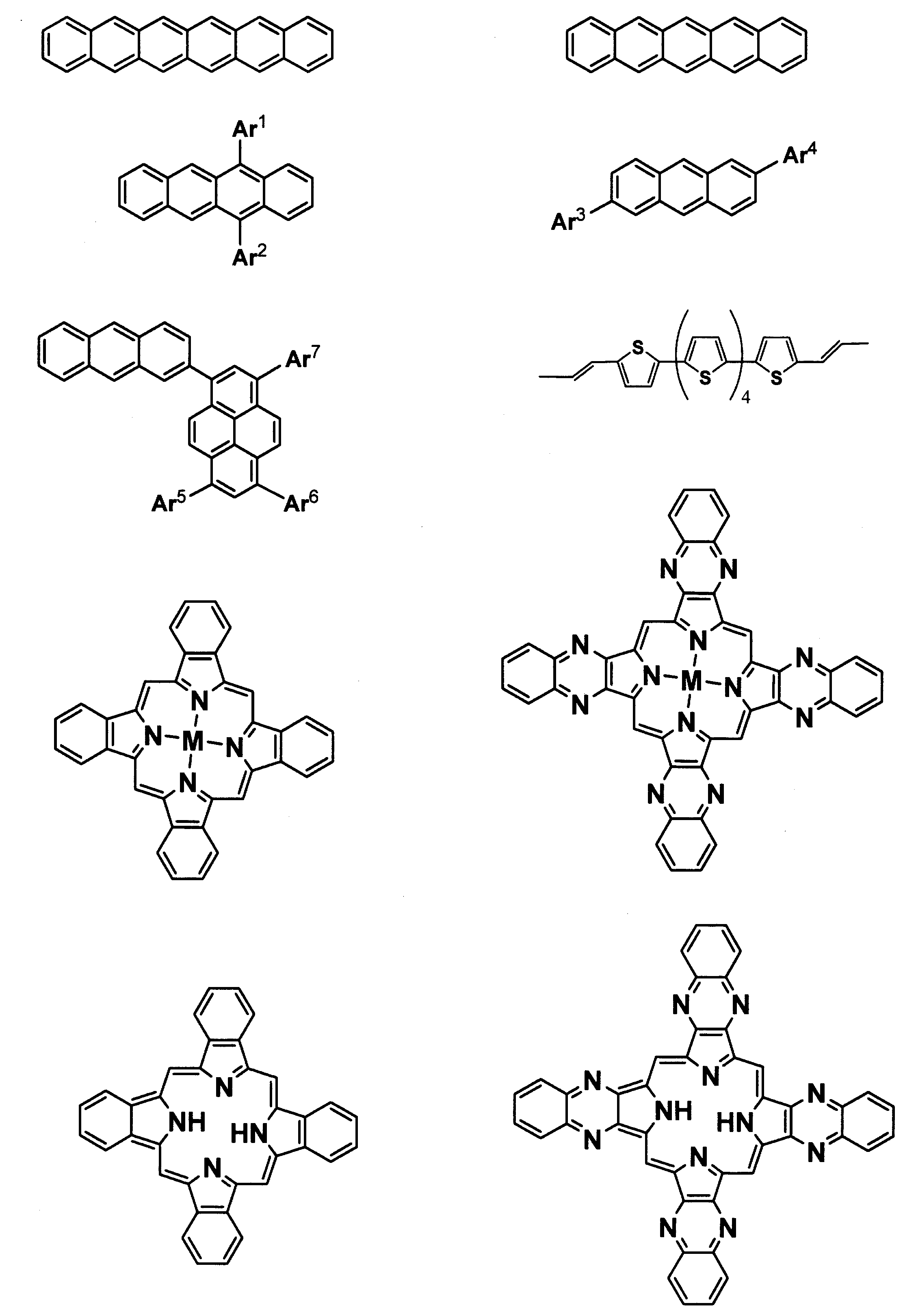
- Ar 1 to Ar 7 each represents hydrogen, an aryl group or a heteroaryl group, which may be substituted.
- the substituent is preferably an aryl group or a heteroaryl group.
- the number of carbon atoms including the substituent is preferably 1 to 20.
- Ar 1 and Ar 2 , Ar 3 and Ar 4 , and Ar 5 to Ar 7 may be the same or different.
- M represents a metal ion. Specific examples of M include aluminum, gallium, indium, copper, zinc, iron, cobalt, nickel, rhodium, ruthenium, palladium, platinum and the like.
- a protonated compound instead of a metal ion is also useful as a device constituent material.
- those having a naphthacene skeleton, those having a pentacene skeleton, and those having an anthrylpyrene skeleton are particularly preferable because they exhibit good characteristics as a light-emitting material or an organic semiconductor.
- Examples of producing organic EL devices using these device constituent materials include Japanese Patent No. 3196230, International Publication WO2007 / 097178, Japanese Patent Application Laid-Open No. 2002-8867, Japanese Patent Application Laid-Open No. 2008-159778, and the like.
- Examples of manufacturing organic transistors are “Chemistry of Materials”, 2004, 16, 23, 4413-4422, “Chemical Review”, 2007, 107, 4, 1066-1096, JP 2004 -015007 and the like.
- Examples of producing the organic solar cell include Japanese Patent Application Laid-Open No. 2004-055586, Japanese Patent Application Laid-Open No. 2005-166744, and Japanese Patent Application Laid-Open No. 2008-135622.
- the present invention can be applied by preparing a solvent-soluble precursor for the device materials described in these examples.
- solvent soluble refers to the solubility at which a solution having a concentration of 0.5 weight percent or more can be adjusted with respect to any one or more of the following solvents at room temperature and atmospheric pressure. More preferably, 1.0 weight percent, or even 3.0 weight percent or more of the solution can be adjusted.
- the solvent is not particularly limited, it is preferable that the solution having the above-mentioned concentration can be adjusted and has a boiling point, viscosity, and surface tension suitable for the coating process. Specifically, water, alcohol having a boiling point of 100 ° C. or higher and 250 ° C.
- xylene, benzoic acid ester, tetralin and cyclohexanone are preferably used. It is also possible to use a mixture of a plurality of these solvents. Further, since impurities contained in the solvent may deteriorate the characteristics of the manufactured device, it is desirable to use a high-purity product as much as possible.
- the solution for coating can be adjusted by putting the precursor material and solvent in a container and stirring. At this time, dissolution can be promoted by heating or ultrasonic waves.
- the donor substrate can be used without particular limitation as long as it can apply a precursor material to form a transfer layer and can be used for transfer to a device substrate.
- partition patterns partition walls
- a surface treatment may be performed on the donor substrate so that a good film can be obtained when the precursor material is applied, or a material having physical properties necessary for transfer may be formed on the donor substrate in advance.
- the surface treatment is a treatment for controlling the wettability of the coating solution, and examples thereof include a silane-based hydrophilic treatment agent and a “Teflon” (registered trademark) water-repellent treatment agent.
- the material having physical properties required at the time of transfer include a heat insulating material, a photothermal conversion material, a reflective material, a drying material, a polymerization initiator, a polymerization inhibitor, and an insulating material.
- an inkjet method As a method of applying the precursor material, an inkjet method, a spin coating method, a blade coating method, a slit die coating method, a screen printing method, a bar coater method, a mold method, a nozzle method, a printing transfer method, a dip pulling method, a spray method, etc. Can be mentioned.
- the ink-jet method, the screen printing method, the nozzle method, the print transfer method, and the like are suitably used for those that require patterning, such as an organic EL element and an organic transistor element.
- the precursor material coating solution is preferably adjusted to a concentration of 1 to 5% by weight using the solvent. More preferably, it is 3 to 5% by weight.
- the film thickness of the precursor material is not particularly limited as long as it is greater than the film thickness necessary for the converted device material, but is usually about 20 to 200 nm, preferably 10 to 100 nm, and more preferably 20 to 50 nm. It is desirable that the thin film formed by coating has a uniform film thickness without pinholes.
- the donor substrate after the precursor material has been applied can be left to dry in an inert atmosphere under atmospheric pressure, but it can be left under reduced pressure to reduce residual solvent, or under an inert gas flow. It is also preferable to leave it stationary. Furthermore, heating on a hot plate or in an inert oven also has an effect of reducing the residual solvent, and these methods can be combined.
- heating since it is preferable to carry out at the minimum temperature in order to prevent decomposition
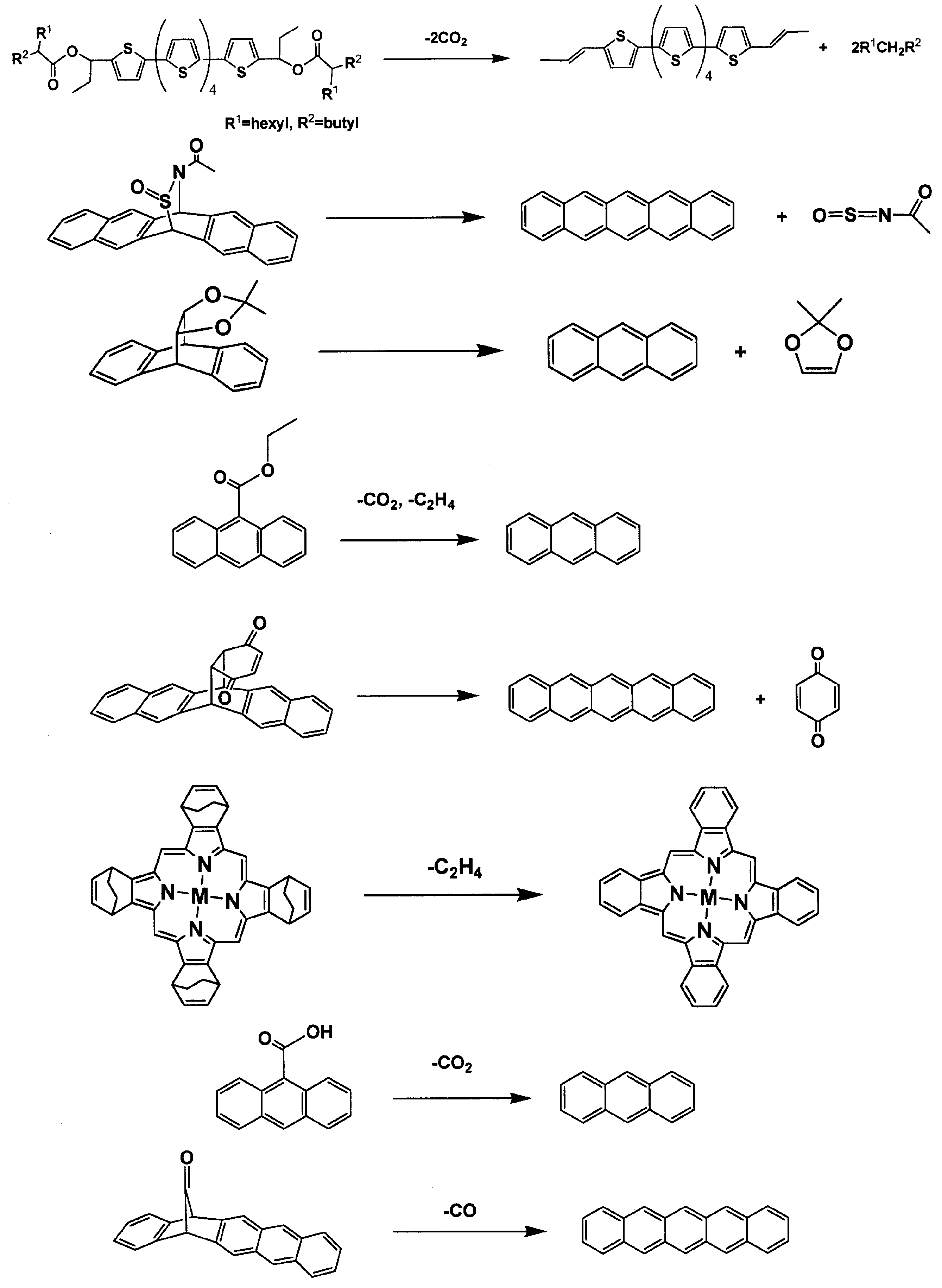
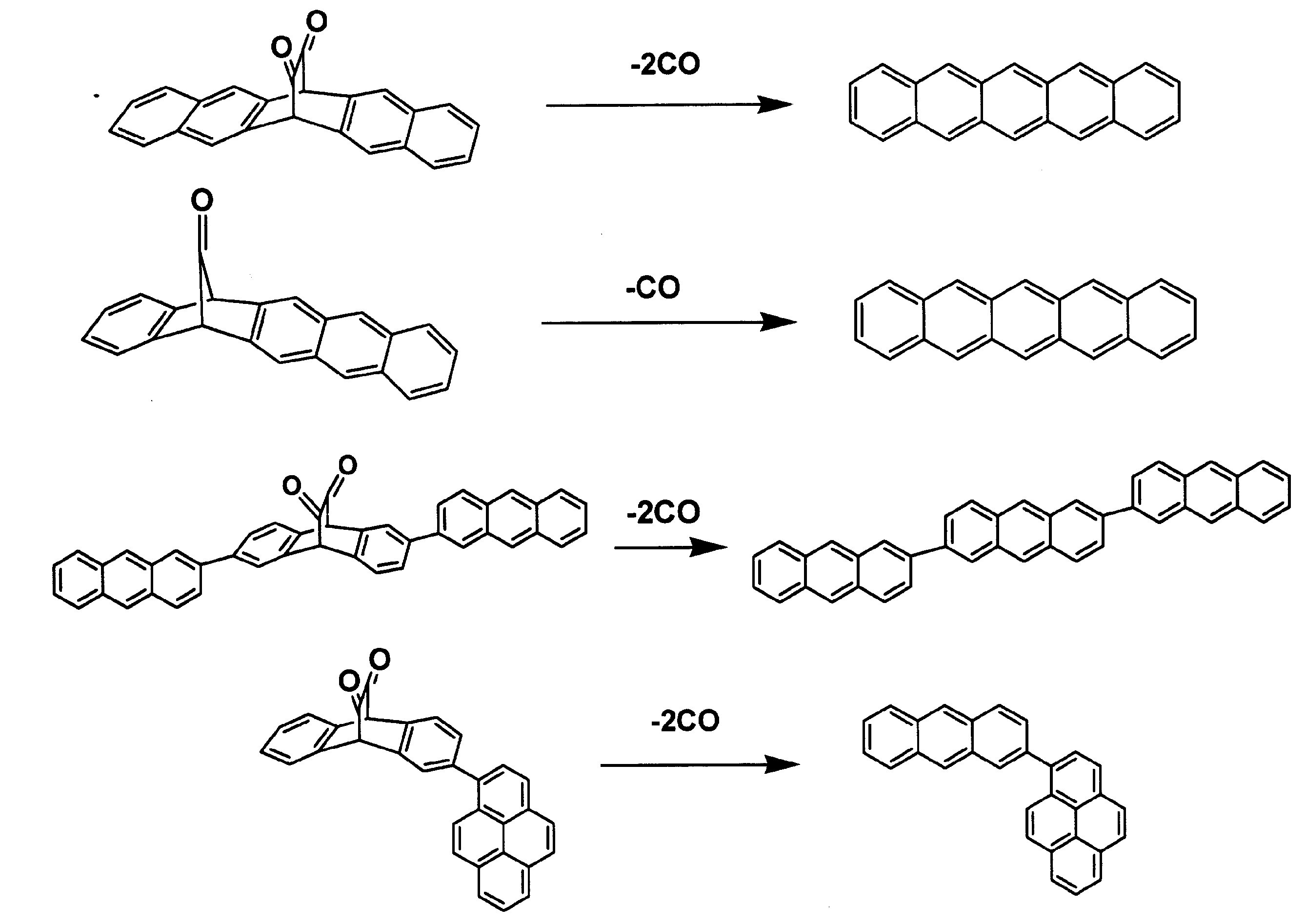
- the conversion step causes a structural change of the precursor material by heating, light irradiation, contact with a chemical solution, etc., and conversion into the target device constituent material. It is a process to do. In this case, as a factor causing the structural change, those which do not remain in the constituent materials such as heat, light, and volatile compounds are preferable in order not to deteriorate the characteristics of the device. Volatile compounds refer to acids and alkalis that do not remain after hydrochloric acid ether complexes, ammonia gas, and the like. Among these structural changes, a structural change by light irradiation and / or heat treatment is particularly preferable.
- the conversion is preferably performed at the lowest possible temperature. Therefore, it is preferable to use a precursor that can be converted at 180 ° C. or lower. Examples of structural changes are due to desorption of small molecules such as ethylene, carbon monoxide and carbon dioxide from the precursor material as described later. Among them, those where ethylene and carbon monoxide are desorbed are 180 ° C or less. Conversion is possible and is preferable. A hot plate, an inert oven, an infrared heater, or the like can be used for heating.
- the structure when converted by light irradiation, it is preferable to irradiate visible light. This is because an undesired reaction due to ultraviolet light (light having a wavelength of less than 390 nm) may occur depending on the precursor used. Therefore, when such an undesirable reaction does not occur, for example, white light may be irradiated as it is. However, when an undesirable reaction occurs, light with little or no ultraviolet light is irradiated. Is preferred. For example, a method of irradiating the precursor with light emitted from a light source after passing through an ultraviolet cut filter is preferable.
- the more preferable wavelength of irradiation light depends on the precursor material used, but when using a precursor (a precursor having a keto-crosslinking and / or diketo-crosslinking structure) that generates carbon monoxide and converts it into a device material, which will be described later. It is particularly preferable to use blue light that allows efficient conversion. Specifically, it is preferable to use light having a peak wavelength in the range of 430 to 470 nm and a half width of the peak of 50 nm or less. Compounds that generate carbon monoxide and convert it into device materials show absorption in this wavelength region due to the carbonyl group's n- ⁇ * transition. This absorption is not greatly dependent on the structure of the compound. Since the conversion reaction from the precursor to the device material accompanied by the release of carbon monoxide proceeds when the precursor is excited by the absorption of light in this wavelength region, the light in the above wavelength region may be irradiated. Particularly preferred.
- the light source for light irradiation a combination of a high-intensity light source lamp and a band pass filter, a light emitting diode, or the like can be used.
- the high-intensity light source lamp include, but are not limited to, a high-pressure mercury lamp, a halogen lamp, and a metal halide lamp.
- the heating temperature is preferably 150 ° C. or less, more preferably 40 to 100 ° C.
- the structure when the structure is converted by contact with a chemical solution, a method of immersing the substrate in a storage layer in which the chemical solution is stored, a method of spraying a chemical solution, or the like can be exemplified. In either case, the conversion may be promoted by heating after contact with the chemical solution. Moreover, you may introduce the process of wash
- the conversion reaction examples include a Retro Diels-Alder reaction, a cheletropy reaction, a decarboxylation reaction, an ester decomposition reaction, and a decarbonylation reaction from a carbonyl compound.
- M is aluminum, gallium, indium, copper, zinc, iron, cobalt, nickel, rhodium, ruthenium, palladium, platinum or the like.
- Examples of structural changes due to light include the following.
- Examples of the precursor material synthesis method include a method of synthesizing a target precursor material by a Diels-Alder reaction using a device constituent material, and a method of chemically synthesizing a precursor material from other raw materials. Specifically, it is synthesized by the method described in JP-A-2003-304014, JP-A-2004-266157, JP-A-2005-232136, “Tetrahedron Letters”, 2005, 46, 1981-1983. can do.
- the conversion process is preferably carried out in an inert atmosphere in order to avoid contact with moisture / oxygen as much as possible, which degrades materials and reduces device characteristics.
- the inert atmosphere is, for example, a rare gas atmosphere such as argon, helium, or xenon, or a nitrogen or carbon dioxide atmosphere. Among these, argon, helium or nitrogen is preferably used, and argon or nitrogen is more preferably used.
- the precursor in the present invention can be used in various reaction forms as described above. Among them, a precursor that generates carbon monoxide and converts it into a device material (having a keto-crosslinking and / or diketo-crosslinking structure).
- a (precursor) is preferable because moisture and oxygen mixed in a trace amount in the donor substrate can be removed. That is, carbon monoxide generated in the thin film reacts with water and oxygen present in the thin film by heating and / or light irradiation to generate hydrogen, carbon dioxide, and the like. This removes moisture and oxygen.
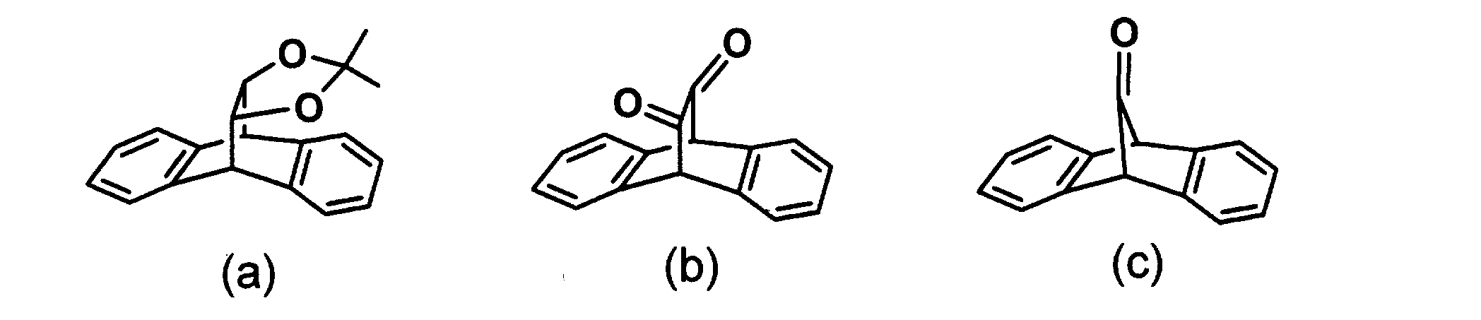
- the keto cross-linked structure referred to here is a structure having a bicyclo skeleton having a cross-linked carbonyl group as shown in Chemical Formula 1 (c).
- the diketo cross-linked structure is a structure having an ⁇ -diketo cross-linked bicyclo skeleton as shown in Chemical Formula 1 (b).
- Examples of useful precursors for generating carbon monoxide and converting it into device materials include the following.
- Ar 1 to Ar 7 represent hydrogen, an aryl group, or a heteroaryl group, which may or may not be substituted. Ar 1 to Ar 7 may be the same or different. When Ar 1 to Ar 7 are an aryl group or a heteroaryl group, the number of carbon atoms including substituents is preferably 1 to 20. Specific examples include those described in International Publication WO 2007/097178 pamphlet and Japanese Patent No. 3712760.
- the transfer process is a process of superimposing the device substrate and the donor substrate and transferring the material on the donor substrate to the device substrate by heating or light irradiation. .
- a known method can be used as the overlay method.
- the space between the donor substrate and the device substrate is preferably a vacuum or a reduced pressure atmosphere of 0.01 Torr or less.
- an inert atmosphere may be used if necessary.
- a known method can be used for the transfer step, and examples thereof include a method of heating the superimposed donor substrate and device substrate from the donor substrate side, and a method of irradiating light from the donor substrate side. Heating can be performed using a hot plate or an infrared heater. Moreover, if it is a donor board
- the light irradiated at this time is preferably a laser beam capable of selecting the center wavelength, irradiation intensity, and irradiation range.
- the transfer with the laser beam may be completed at a time or may be completed a plurality of times.
- the laser beam may be irradiated by scanning, step irradiation or batch irradiation.
- the material on the donor substrate is finally heated and transferred onto the device substrate by sublimation. Therefore, it is possible to form a film that is as homogeneous as when vapor deposition is used, and a high-performance device can be obtained.
- FIG. 1 is a cross-sectional view showing an example of a method for irradiating a donor substrate with light according to the present invention.
- the donor substrate 30 is composed of a support 31, a photothermal conversion layer 33, and one kind of device constituent material 37
- the transfer substrate 20 is composed only of the support 22.
- FIG. 1B light represented by a laser is incident from the support 31 side of the donor substrate 30, and the light is applied to the photothermal conversion layer 33 so that a part of the device constituent material 37 is heated. Irradiation enables transfer to the transfer substrate.
- FIG. 1B schematically shows a process in which the device constituent material 37 is heated and evaporated to be deposited on the support 22 of the device substrate 20 as the transfer film 27.
- the light irradiation can be stopped (the light irradiation of the portion is terminated by the movement of the light irradiation portion), or the light irradiation can be continued as it is to transfer the entire device constituent material 37.
- an ablation mode in which the device constituent material 37 reaches the support 22 of the device substrate 20 in a state where the film shape is maintained can also be used.
- the device constituent material 37 is transferred in a plurality of times in the film thickness direction.
- This is a preferred transfer method.
- the maximum temperature of not only the device constituent material 37 but also the underlying layer formed on the device substrate 20 can be lowered, so that damage to the donor substrate and device performance can be prevented.
- the number n is not limited. However, if the amount is too small, the above-mentioned effect under low temperature is not sufficiently exhibited. The range of is preferable.
- FIG. 2 shows the width of each of two or more different device constituent materials 37 (in this example, three types of 37R, 37G, and 37B) and a partition pattern 34 (in this example, a partition sandwiched between 37R and 37G, 37G and 37B).
- a partition pattern 34 in this example, a partition sandwiched between 37R and 37G, 37G and 37B.
- the set of transfer materials 37R, 37G, and 37B is k times in the x direction of the arrangement, In the case where it is repeatedly formed h times in the vertical y direction, for example, m sets (m is a number of 2 to k) transfer materials 37R, 37G, and 37B are simultaneously irradiated with light while light is applied in the y direction. Can be shortened to about 1 / m.
- the entire transfer material is collectively transferred in one scan by irradiating light that covers the entire width of the transfer region 38 of the donor substrate 30. You can also With this arrangement, alignment of light irradiation with respect to the donor substrate 30 can be greatly reduced.
- FIG. 3B when there are a plurality of transfer regions 38 on the substrate, it is also possible to transfer them all at once. As is called a delta arrangement, even when the RGB sub-pixels are not arranged in a straight line, the irradiation light can be scanned in a straight line, so that the transfer can be easily performed.
- the conversion step (2) is performed before the transfer step (3) (Method I), or the conversion step (2) is performed simultaneously with the transfer step (3).
- the embodiment (Method II) is preferred.
- Method I after the precursor material is applied on the donor substrate, the conversion to the device material is performed by the above-described method, and then the transfer to the device substrate is performed.
- Method II after the precursor material is applied on the donor substrate, the donor substrate and the device substrate are overlapped and transferred to the device substrate. Then, transfer is performed while the precursor material is converted into a device material.
- the method I is preferable because the conversion from the precursor material to the device material can be performed uniformly and at a high conversion rate.
- FIG. 5 is a cross-sectional view showing an example of a typical structure of the organic EL element 10 (display).
- An active matrix circuit including the TFT 12 and the planarization layer 13 is formed on the support 11.
- the element portion is the first electrode 15 / hole transport layer 16 / light emitting layer 17 / electron transport layer 18 / second electrode 19 formed thereon.
- An insulating layer 14 that prevents a short circuit from occurring at the electrode end and defines a light emitting region is formed at the end of the first electrode.
- the configuration of the element is not limited to this example. For example, only one light emitting layer having a hole transport function and an electron transport function may be formed between the first electrode and the second electrode.
- the hole transport layer may be a hole injection layer and a hole transport layer
- the electron transport layer may be a multilayer structure of an electron transport layer and an electron injection layer
- the light emitting layer has an electron transport function.
- the electron transport layer may be omitted.
- these layers may be a single layer or a plurality of layers.
- a protective layer, a color filter, sealing, or the like may be performed using a known technique.
- the light emitting layer In a color display, at least a light emitting layer needs to be patterned, and the light emitting layer is a thin film that is suitably patterned in the present invention.
- the insulating layer, the first electrode, the TFT, and the like are often patterned by a known photolithography method, but may be patterned using the method of the present invention.
- at least one layer such as a positive hole transport layer, an electron carrying layer, and a 2nd electrode
- the photolithographic method is used up to the first electrode 15, the insulating layer 14 is patterned by a known technique using a photosensitive polyimide precursor material, and then the hole transport layer 16 is used. Is formed on the entire surface by a known technique using a vacuum deposition method. Then, the light emitting layers 17R, 17G, and 17B are patterned on the hole transport layer 16 through the steps (1) to (3). On top of this, if the electron transport layer 18 and the second electrode 19 are formed on the entire surface by a known technique such as vacuum deposition, an organic EL element can be completed.
- FIG. 6 is a cross-sectional view showing an example of a transfer process in this production example.
- the donor substrate 30 includes a support 31, a light-to-heat conversion layer 33, a partition pattern 34, and a light emitting material 37 existing in the partition pattern (an organic EL RGB light emitting material precursor is applied and then a skeleton is formed on the light emitting material Converted).
- the partition pattern 34 of the donor substrate 30 and the insulating layer 14 of the device substrate 10 are aligned, the two substrates are arranged to face each other.
- a laser is incident from the support 31 side of the donor substrate 30 and absorbed by the photothermal conversion layer 33, and the light emitting materials 37R, 37G, and 37B are simultaneously heated and evaporated by the heat generated there, and they are transported by holes of the device substrate 10.
- the light emitting layers 17R, 17G, and 17B are collectively formed.
- the light emitting layer may be a single layer or a plurality of layers, and the light emitting material of each layer may be a single material or a mixture of a plurality of materials.
- the light emitting layer preferably has a single layer structure of a mixture of a host material and a dopant material. Therefore, the transfer material for forming the light emitting layer is preferably a mixture of a host material and a dopant material.
- the precursor material that becomes a host material after conversion it is preferable to use a precursor material that becomes a host material after conversion. A mixed solution of such a precursor material and a dopant material is applied onto a donor substrate, dried, and then a subsequent conversion step and transfer. Through the steps, a light emitting layer can be formed.
- the concentration of the dopant material in the light emitting layer can be changed in the film thickness direction by utilizing the difference in evaporation temperature between the precursor material or the host material and the dopant material at the time of transfer.
- Examples of light-emitting materials include anthracene derivatives, naphthacene derivatives, pyrene derivatives, quinolinol complexes such as tris (8-quinolinolato) aluminum (Alq 3 ), and benzothiazolyl
- Various metal complexes such as phenol-zinc complexes, bisstyrylanthracene derivatives, tetraphenylbutadiene derivatives, coumarin derivatives, oxadiazole derivatives, benzoxazole derivatives, carbazole derivatives, distyrylbenzene derivatives, pyrrolopyridine derivatives, perinone derivatives, cyclopentadiene derivatives, Oxadiazole derivatives, thiadiazolopyridine derivatives, rubrene, quinacridone derivatives, phenoxazone derivatives, perinone derivatives, perylene derivatives, coumarin derivatives, chrysene Conduct
- examples of materials excellent in light emitting performance and suitable for the production method of the present invention include anthracene derivatives, naphthacene derivatives, pyrene derivatives, chrysene derivatives, pyromethene derivatives, and various phosphorescent materials.
- the hole transport layer may be a single layer or a plurality of layers, and each layer may be a single material or a mixture of a plurality of materials.
- a layer called a hole injection layer is also included in the hole transport layer. From the viewpoint of hole transportability (low driving voltage) and durability, an acceptor material that promotes hole transportability may be mixed in the hole transport layer. Therefore, the transfer material for forming the hole transport layer may be made of a single material or a mixture of a plurality of materials.
- hole transport materials include N, N′-diphenyl-N, N′-dinaphthyl-1,1′-diphenyl-4,4′-diamine (NPD) and N, N′-biphenyl-N, N′—.
- aromatic amines N-isopropylcarbazole, pyrazoline derivatives, stilbene compounds, hydrazone compounds, low molecular materials such as oxadiazole derivatives and heterocyclic compounds represented by phthalocyanine derivatives, and these low molecules
- polymer materials such as polycarbonate having a compound in the side chain, styrene derivative, polyvinyl carbazole, and polysilane.
- acceptor material examples include low molecular weight materials such as 7,7,8,8-tetracyanoquinodimethane (TCNQ), hexaazatriphenylene (HAT) and its cyano group derivative (HAT-CN6).
- TCNQ 7,7,8,8-tetracyanoquinodimethane
- HAT hexaazatriphenylene
- HAT-CN6 cyano group derivative
- metal oxides such as molybdenum oxide and silicon oxide that are thinly formed on the surface of the first electrode can also be exemplified as hole transport materials and acceptor materials.
- the electron transport layer may be a single layer or a plurality of layers, and each layer may be a single material or a mixture of a plurality of materials.
- a layer called a hole blocking layer or an electron injection layer is also included in the electron transport layer.
- the electron transport layer may be mixed with a donor material that promotes electron transport properties.
- a layer called the electron injection layer is often discussed as this donor material.
- the transfer material for forming the electron transport layer may be made of a single material or a mixture of a plurality of materials.
- electron transport materials include quinolinol complexes such as Alq 3 and 8-quinolinolatolithium (Liq), condensed polycyclic aromatic derivatives such as naphthalene and anthracene, and 4,4′-bis (diphenylethenyl) biphenyl.
- quinolinol complexes such as Alq 3 and 8-quinolinolatolithium (Liq)
- condensed polycyclic aromatic derivatives such as naphthalene and anthracene
- 4,4′-bis (diphenylethenyl) biphenyl 4,4′-bis (diphenylethenyl) biphenyl.
- Styryl aromatic ring derivatives such as anthraquinone and diphenoquinone, phosphorus oxide derivatives, benzoquinolinol complexes, hydroxyazole complexes, azomethine complexes, various metal complexes such as tropolone metal complexes and flavonol metal complexes, heterocycles containing electron-accepting nitrogen Examples thereof include low molecular materials such as compounds having an aryl ring structure, and polymer materials having these low molecular compounds in the side chain.
- the donor material examples include alkali metals and alkaline earth metals such as lithium, cesium, magnesium, and calcium, various metal complexes such as quinolinol complexes, and oxides and fluorides such as lithium fluoride and cesium oxide. be able to.
- An electron transport material or a donor material is one of materials that easily change in performance due to the combination with each of the RGB light emitting layers, and is exemplified as another preferable example that is patterned by the present invention. It is preferable that at least one of the first electrode and the second electrode is transparent in order to extract light emitted from the light emitting layer.
- the first electrode In the case of bottom emission in which light is extracted from the first electrode, the first electrode is transparent, and in the case of top emission in which light is extracted from the second electrode, the second electrode is transparent. Also, at the time of transfer, reactive transfer can be performed, for example, by reacting a transfer material with oxygen.
- the transparent electrode material and the other electrode conventionally known materials can be used as described in JP-A-11-214154, for example.
- the organic EL element in the present invention is not generally limited to the active matrix type in which the second electrode is formed as a common electrode.
- the organic EL element is formed of a stripe electrode in which the first electrode and the second electrode intersect each other. It may be a simple matrix type or a segment type in which the display unit is patterned so as to display predetermined information. Examples of these applications include televisions, personal computers, monitors, watches, thermometers, audio equipment, automobile display panels, and the like.
- the organic EL device manufactured by the method of the present invention has a high performance in terms of luminous efficiency and lifetime as well as those manufactured by the vapor deposition method.
- a large organic EL element that is difficult to produce by a vapor deposition method can be produced, and even in that case, an element excellent in luminous efficiency and life can be obtained.
- the device manufacturing method of the present invention is applicable not only to organic EL elements but also to devices such as organic TFTs, photoelectric conversion elements, and various sensors.
- a typical organic TFT for manufacturing an organic TFT having a source electrode, a drain electrode, an organic semiconductor layer formed between them, a gate insulating layer, and a gate electrode, as an example, the present invention is as follows. Can be applied. First, a gate electrode and a gate insulating layer, a source electrode and a drain electrode are formed on a substrate by a known method to obtain a device substrate.
- a solution in which a solvent-soluble precursor of a material for forming the organic semiconductor layer is dissolved in an appropriate solvent is applied on another substrate, and this is used as a donor substrate. Then, the precursor is converted into an organic semiconductor layer forming material by the method of the present invention, the donor substrate and the device substrate are made to face each other, and then transferred to a predetermined position on the device substrate. Then, an organic TFT can be manufactured by forming a sealing film by a well-known method or the method of this invention as needed.
- the material for forming the substrate, the source electrode, the drain electrode, the gate insulating layer, and the gate electrode is not particularly limited, and for example, known materials such as those described in JP-A-2006-173444 can be used.
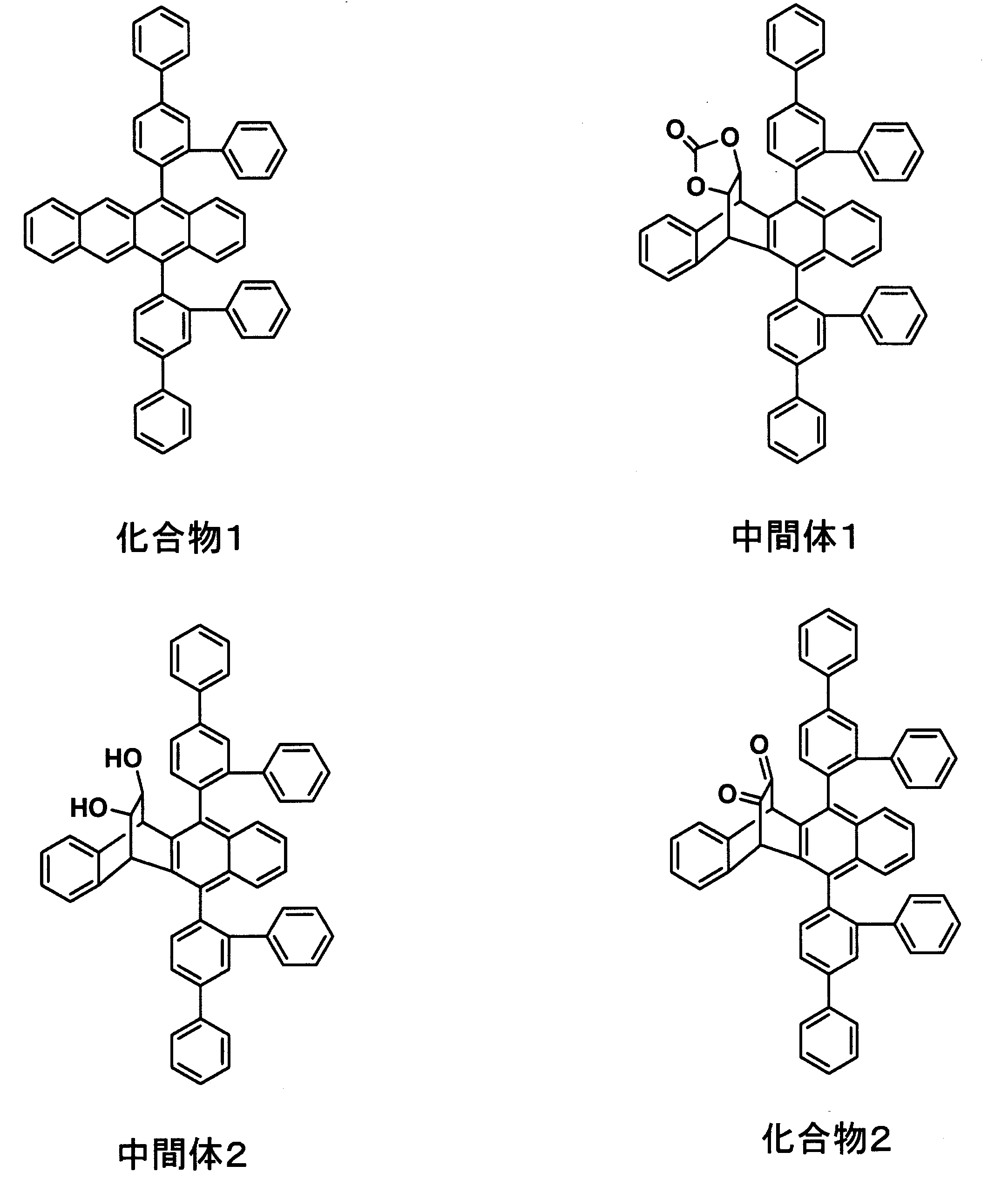
- Synthesis example 1 Synthesis of Intermediate 1 Compound 1 (0.48 g) and vinylene carbonate (0.1 mL) were heated and distilled in orthodichlorobenzene (10 mL) for 15 hours. After cooling the reaction solution to room temperature, a large excess of hexane was added and stirred vigorously. The resulting powdered solid was filtered and dried to obtain Intermediate 1 as a white powder. Intermediate 1 was a mixture of isomers. Yield 0.53 g (98%). 1 H-NMR ( ⁇ : ppm) 7.93-6.75 (m, 34H), 4.88-4.23 (m, 4H).
- Compound 1 could not prepare a solution of 0.5% by weight or more in any solvent of dichlorobenzene, chloroform, tetralin, ethyl benzoate and N-methyl-2-pyrrolidone. It was possible to prepare a solution of 2% by weight or more with respect to any of these solvents.
- Synthesis example 2 Synthesis of Intermediate 3 Compound 3 (0.53 g) and vinylene carbonate (0.1 mL) were heated and distilled in orthodichlorobenzene (10 mL) for 15 hours. After cooling the reaction solution to room temperature, a large excess of hexane was added and stirred vigorously. The resulting powdered solid was filtered and dried to obtain Intermediate 3 as a white powder. Intermediate 3 was a mixture of isomers. Yield 0.56 g (99%). 1 H-NMR ( ⁇ : ppm) 8.03-7.01 (m, 20H), 4.89-4.45 (m, 4H).
- Compound 3 could not prepare a solution of 0.5 wt% or more in any solvent of dichlorobenzene, chloroform, tetralin, ethyl benzoate, and N-methyl-2-pyrrolidone. It was possible to prepare a solution of 2% by weight or more with respect to any of these solvents.
- Example 1 A donor substrate was prepared as follows. An alkali-free glass substrate was used as a support, and after cleaning / UV ozone treatment, a titanium film having a thickness of 1.0 ⁇ m was formed as a photothermal conversion layer on the entire surface by sputtering. Next, after the photothermal conversion layer has been subjected to UV ozone treatment, a positive polyimide photosensitive coating agent (DL-1000, manufactured by Toray Industries, Inc.) is spin-coated thereon, prebaked and UV exposed, and then a developer. The exposed part was dissolved and removed by ELM-D (manufactured by Toray Industries, Inc.). The polyimide precursor film thus patterned was baked on a hot plate at 350 ° C.
- DL-1000 positive polyimide photosensitive coating agent
- the partition pattern had a height of 2 ⁇ m and a cross section of a forward tapered shape. Openings exposing the photothermal conversion layer having a width of 80 ⁇ m and a length of 280 ⁇ m were arranged in the partition pattern at a pitch of 100 and 300 ⁇ m, respectively.
- a chloroform solution containing 3% by weight of Compound 2 and 0.15% by weight of DCJTB shown below was spin-coated and dried.
- the obtained thin film was irradiated with light (peak wavelength: 405 nm (half width: 5 nm), 436 nm (half width: 5 nm)) of a high pressure mercury lamp (600 W) passed through a blue filter in a nitrogen atmosphere for 3 hours. Converted to. As a result, a layer having an average thickness of 25 nm composed of Compound 1 and DCJTB was formed in the partition pattern (opening).
- the device substrate was produced as follows. A non-alkali glass substrate (manufactured by Geomatic Co., Ltd., sputtering film-formed product) on which an ITO transparent conductive film was deposited to 140 nm was cut into 38 ⁇ 46 mm, and the ITO was etched into the shape shown in FIG. 7 by photolithography. Next, the polyimide precursor film patterned similarly to the donor substrate was baked at 300 ° C. for 10 minutes to form a polyimide-based insulating layer. The height of this insulating layer was 1.8 ⁇ m and the cross section was a forward tapered shape.
- Openings exposing ITO with a width of 70 ⁇ m and a length of 270 ⁇ m were arranged in the pattern of the insulating layer at a pitch of 100 and 300 ⁇ m, respectively.
- This substrate was subjected to UV ozone treatment, placed in a vacuum deposition apparatus, and evacuated until the degree of vacuum in the apparatus became 3 ⁇ 10 ⁇ 4 Pa or less.
- 20 nm of copper phthalocyanine (CuPc) and 40 nm of NPD were stacked as a hole transport layer by vapor deposition over the entire light emitting region.
- the partition pattern of the donor substrate and the insulating layer of the device substrate were aligned and held in a vacuum of 3 ⁇ 10 ⁇ 4 Pa or less, and then taken out into the atmosphere.
- the transfer space partitioned by the insulating layer and the partition pattern was kept in a vacuum.
- a laser having a central wavelength of 800 nm (light source: semiconductor laser diode) is irradiated from the glass substrate side of the donor substrate so that a part of the material in the partition pattern and a part of the partition pattern are heated simultaneously.
- the material in the partition pattern was transferred onto the hole transport layer which is the underlayer of the device substrate.
- the laser intensity was about 300 W / mm 2
- the scanning speed was 1.25 m / s
- repeated scanning was performed by overlapping the lasers so as to be transferred over the entire light emitting region.
- the transferred device substrate was placed in the vacuum deposition apparatus again and evacuated until the degree of vacuum in the apparatus became 3 ⁇ 10 ⁇ 4 Pa or less.
- E-1 shown below as an electron transporting layer was deposited on the entire surface of the light emitting region by resistance heating.
- lithium fluoride was deposited at a thickness of 0.5 nm as a donor material (electron injection layer), and aluminum was deposited at a thickness of 100 nm as a second electrode to produce an organic EL device having a 5 mm square light emitting region.
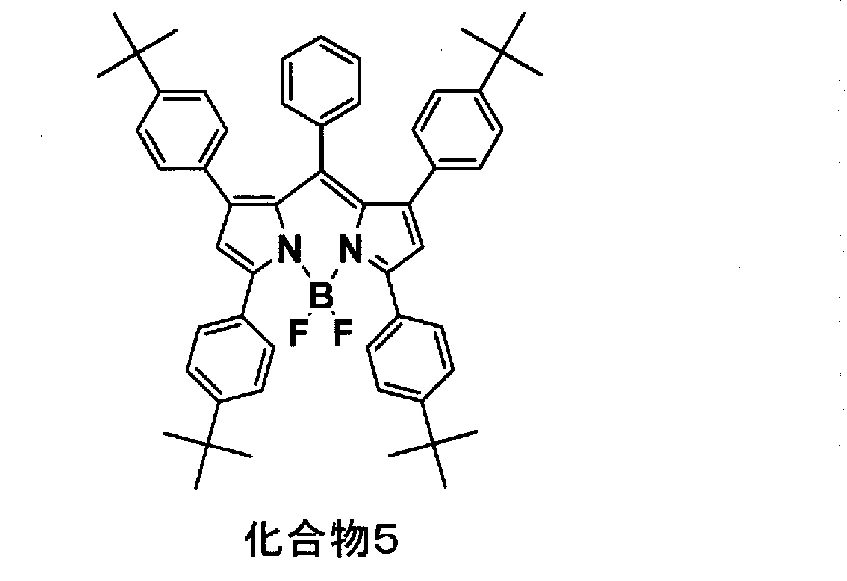
- Example 2 An organic EL device was produced in the same manner as in Example 1 except that the following compound 5 was used instead of DCJTB.
- Example 3 Instead of laminating copper phthalocyanine and NPD as a hole transport layer by vacuum deposition, PEDOT ⁇ poly (3,4-ethylenedioxythiophene) ⁇ : PSS ⁇ poly (4-styrenesulfonate) ⁇ aqueous solution (PEDOT 0.8 wt% , PSS 0.5 wt%) was formed to a thickness of 100 nm by spin coating, and an organic EL device was produced in the same manner as in Example 2 except that it was dried by heating at 200 ° C. for 5 minutes using a hot plate.
- PEDOT ⁇ poly (3,4-ethylenedioxythiophene) ⁇ PSS ⁇ poly (4-styrenesulfonate) ⁇ aqueous solution (PEDOT 0.8 wt% , PSS 0.5 wt%) was formed to a thickness of 100 nm by spin coating, and an organic EL device was produced in the same manner as in Example 2 except that it was dried by heating at 200 ° C. for
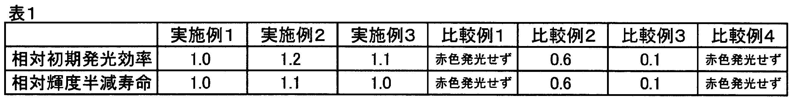
- Comparative Example 1 An organic EL device was prepared in the same manner as in Example 1 except that a coating film was prepared using a chloroform suspension of compound 1 and DCJTB instead of the chloroform solution of compound 2 and DCJTB, and a donor substrate was prepared without light irradiation. A device was created. Since compound 1 has low solubility, a 3 wt% chloroform solution could not be prepared and was used as a suspension. In this case, the film thickness of the material layer on the donor substrate was not uniform, and a good transfer film could not be obtained. Further, although the compound 1 was adhered on the device substrate after the transfer, the film quality was poor, and EL light emission from the compound 1 or DCJTB could not be observed from the prepared element.
- Comparative Example 2 Instead of forming the light emitting material layer on the donor substrate and then transferring it to the device substrate, a chloroform solution containing 3% by weight of Compound 2 and 0.15% by weight of DCJTB is directly spin coated on the device substrate and dried. Under a nitrogen atmosphere, light from a high-pressure mercury lamp (600 W) passed through a blue filter (peak wavelength: 405 nm (half width 5 nm), 436 nm (half width 5 nm)) is irradiated for 3 hours to convert compound 2 into compound 1 and emit light An organic EL device was produced in the same manner as in Example 3 except that the layer was produced.
- a chloroform solution containing 3% by weight of Compound 2 and 0.15% by weight of DCJTB is directly spin coated on the device substrate and dried. Under a nitrogen atmosphere, light from a high-pressure mercury lamp (600 W) passed through a blue filter (peak wavelength: 405 nm (half width 5 nm), 436 nm (half width 5 n
- Comparative Example 3 Instead of forming the light emitting material layer on the donor substrate and then transferring it to the device substrate, a chloroform solution containing 3% by weight of Compound 2 and 0.15% by weight of DCJTB is directly spin coated on the device substrate and dried.
- Example 1 except that a light-emitting layer was produced by irradiating light (peak wavelength: 405 nm (half-value width: 5 nm), 436 nm (half-value width: 5 nm)) of a high-pressure mercury lamp (600 W) passed through a blue filter in a nitrogen atmosphere for 3 hours. In the same manner, an organic EL device was produced.
- Comparative Example 4 Instead of irradiating the donor substrate on which a thin film composed of Compound 2 and DCJTB is irradiated with the light of the high-pressure mercury lamp (600 W) through the blue filter, the light of the high-pressure mercury lamp (600 W) (including light with a wavelength of 390 nm or less) An organic EL device was produced in the same manner as in Example 1 except that direct irradiation was performed. Under this condition, an undesired reaction occurred, so that Compound 2 could not be converted to Compound 1, and EL emission from DCJTB could not be observed.
- Example 4 A donor substrate was produced in the same manner as in Example 1 except that a molybdenum film having a thickness of 0.4 ⁇ m was formed as a photothermal conversion layer over the entire surface by sputtering.
- a thin film composed of compound 4 and DCJTB was prepared on a donor substrate, and the light was emitted from a blue light-emitting diode (center wavelength: 460 nm, half-value width: 20 nm) for 5 minutes instead of a high-pressure mercury lamp passed through a blue filter.
- the conversion step was carried out in the same manner as in Example 1. As a result, a layer having an average thickness of 25 nm made of compound 3 and DCJTB was formed in the partition pattern (opening).
- Example 5 An organic EL device was produced in the same manner as in Example 4 except that Compound 5 was used instead of DCJTB.
- Example 6 Instead of laminating copper phthalocyanine and NPD by a vacuum deposition method as a hole transport layer, a PEDOT: PSS aqueous solution (0.8% by weight of PEDOT, 0.5% by weight of PSS) is formed to a thickness of 100 nm by a spin coating method.
- An organic EL device was produced in the same manner as in Example 4 except that it was dried by heating at 200 ° C. for 5 minutes using a plate.
- Example 7 A solution in which compound 2 and compound 5 are dissolved in tetralin by 1 wt% and 0.05 wt%, respectively, is prepared, applied to a donor substrate by an ink jet method, and dried, whereby compound 2 and compound 5 The mixed film was formed in the partition pattern.
- Compound 2 was converted to compound 1 by irradiating the mixed film with light of a blue light-emitting diode (center wavelength: 460 nm, half-value width: 20 nm) in vacuum for 5 minutes.
- a blue light-emitting diode center wavelength: 460 nm, half-value width: 20 nm
- an organic EL device was produced in the same manner as in Example 4 except that a transfer material having an average film thickness of 40 nm composed of a mixed film of compound 1 and compound 5 was formed in the partition pattern of the donor substrate. However, clear red light emission was confirmed.
- Comparative Example 5 An organic EL device was produced in the same manner as in Example 4 except that a chloroform suspension of compound 3 and DCJTB was used instead of the chloroform solution of compound 4 and DCJTB. In this case, the film thickness of the material layer on the donor substrate was not uniform, and a good transfer film could not be obtained. Further, although the compound 3 was adhered on the device substrate after transfer, the film quality was poor, and EL light emission from the compound 4 and DCJTB could not be observed from the prepared element.
- Comparative Example 6 Similar to Comparative Example 2, except that Compound 4 was used instead of Compound 2, and light of a blue light emitting diode (center wavelength: 460 nm, half-value width: 20 nm) was irradiated for 5 minutes instead of the high-pressure mercury lamp passed through the blue filter. Thus, an organic EL element was produced.
- a blue light emitting diode center wavelength: 460 nm, half-value width: 20 nm
- Comparative Example 7 The same as Comparative Example 3 except that Compound 4 was used instead of Compound 2 and the light of a blue light emitting diode (center wavelength: 460 nm, half width: 20 nm) was irradiated for 5 minutes instead of the high-pressure mercury lamp passed through the blue filter. Thus, an organic EL element was produced.
- a blue light emitting diode center wavelength: 460 nm, half width: 20 nm
- Comparative Example 8 An organic EL device was produced in the same manner as in Comparative Example 4 except that Compound 4 was used instead of Compound 2. Under this condition, Compound 4 could not be converted to Compound 3, and EL emission from DCJTB could not be observed.
- Compound 1 and Compound 3 are materials that are difficult to form by coating, but as in Examples 1 to 6, a precursor material that can be coated and formed is formed on a donor substrate, An element using the compound 1 or the compound 3 can be manufactured by a coating method by transferring after conversion into a device material. Further, as can be seen from the comparison between Examples 1 and 3 and Comparative Examples 2 to 3 and Comparative Examples 6 to 7, the process of converting the precursor material on the donor substrate to the device material, and further transferring it to the device substrate is performed. By including, the characteristic of an element can be improved significantly compared with the process of apply
- the present invention is a thin film patterning technology for organic EL elements, organic TFTs, photoelectric conversion elements, various sensors, and other devices, and is used for display panels used in mobile phones, personal computers, televisions, image scanners, etc. It can be used for manufacturing touch panels, image sensors, and the like.
- Organic EL elements (device substrates) 11 Support 12 TFT (including extraction electrode) DESCRIPTION OF SYMBOLS 13 Planarization layer 14 Insulating layer 15 1st electrode 16 Hole transport layer 17 Light emitting layer 18 Electron transport layer 19 Second electrode 20 Device substrate 22 Support body 27 Transfer film 30 Donor substrate 31 Support body 33 Photothermal conversion layer 34 Partition pattern 37 Device material 38 Transfer area 40 Glass substrate 41 ITO pattern
Landscapes
- Engineering & Computer Science (AREA)
- Manufacturing & Machinery (AREA)
- Physics & Mathematics (AREA)
- Spectroscopy & Molecular Physics (AREA)
- Chemical & Material Sciences (AREA)
- Materials Engineering (AREA)
- Optics & Photonics (AREA)
- Electroluminescent Light Sources (AREA)
- Thin Film Transistor (AREA)
Abstract
Description
以下、これらの工程について順に説明する。
塗布工程は、デバイス基板へ転写するための材料をドナー基板上に塗布する工程である。ここで、本発明に用いられるドナー基板とは、デバイス基板へ転写するための前駆体材料を塗布し、転写層を形成するために用いられる基板をいう。デバイス基板へ転写するための材料としては、塗布時には溶剤可溶性であり、塗布後にデバイス構成材料へと変換できる前駆体材料を用いる。一般に、デバイス構成材料は溶剤可溶性でないものが多い。これに対し、本発明ではその前駆体材料として溶剤可溶性であるものを用いているため、溶剤可溶性でないデバイス材料であっても本工程に適用できる。
変換工程は、加熱、光照射、薬液との接触などによって前駆体材料の構造変化を引き起こし、目的とするデバイス構成材料へと変換する工程である。この場合、構造変化を引き起こす因子としては、熱・光・揮発性化合物など構成材料の内部に残存しないものがデバイスの特性を低下させないために好ましい。揮発性化合物とは、塩酸エーテル錯体、アンモニアガスなど後に残らない酸やアルカリなどを言う。これらの構造変化の中でも、光照射および/または加熱処理による構造変化が特に好ましい。変換して得られた材料の劣化を防ぐため、加熱により構造を変換させる場合には可能な限り低温で変換を行うことが好ましく、そのため、180℃以下で変換できる前駆体を用いることが好ましい。構造変化の例は後述のように前駆体材料からのエチレン、一酸化炭素、二酸化炭素などの小分子の脱離によるものであるが、中でもエチレンや一酸化炭素が脱離するものは180℃以下での変換が可能であり好ましい。加熱にはホットプレートやイナートオーブン、赤外線ヒーターなどを用いることができる。

転写工程は、デバイス基板とドナー基板を重ね合わせ、ドナー基板上の材料を加熱や光照射などによりデバイス基板に転写する工程である。重ね合わせ方法は公知の方法を用いることができる。また、転写の効率を良くするために、ドナー基板とデバイス基板の間の空間は真空もしくは0.01Torr以下の減圧雰囲気であることが望ましい。ただし、必要な場合には不活性雰囲気であっても良い。前記ドナー基板とデバイス基板の間の空間を真空もしくは減圧雰囲気にするために、ドナー基板には絶縁材を用いて隔壁を形成しておき、デバイス基板との密着性を高めておくことが有用である。
ドナー材料としては、リチウムやセシウム、マグネシウム、カルシウムなどのアルカリ金属やアルカリ土類金属、それらのキノリノール錯体などの各種金属錯体、フッ化リチウムや酸化セシウムなどのそれらの酸化物やフッ化物を例示することができる。電子輸送材料やドナー材料は各RGB発光層との組み合わせによる性能変化が起こりやすい材料の1つであり、本発明によりパターニングされる別の好ましい例として例示される。 第一電極および第二電極は、発光層からの発光を取り出すために少なくとも一方が透明であることが好ましい。第一電極から光を取り出すボトムエミッションの場合には第一電極が、第二電極から光を取り出すトップエミッションの場合には第二電極が透明である。また、転写の際に、例えば転写材料と酸素を反応させるなど、反応性転写を実施することもできる。透明電極材料およびもう一方の電極には、例えば、特開平11-214154号公報記載の如く、従来公知の材料を用いることができる。
中間体1の合成
化合物1(0.48g)と炭酸ビニレン(0.1mL)をオルトジクロロベンゼン(10mL)中15時間加熱乾留した。室温まで反応液を冷却後、大過剰のヘキサンを加えて激しく撹拌した。生じた粉末固体をろ過して乾燥することで中間体1を白色粉末として得た。中間体1は異性体の混合物であった。収量0.53g(98%)。1H-NMR(δ:ppm) 7.93-6.75(m、34H)、4.88-4.23(m、4H)。
中間体1(0.33g)を1,4-ジオキサン(20mL)に溶解し、窒素雰囲気で水酸化ナトリウム水溶液(4N,7.5mL)を加えた後、6時間加熱還流した。反応終了後、水(50mL)を加えて撹拌し、さらにジクロロメタン(50mL)を加えて撹拌した。有機層を分液して飽和食塩水で洗浄し、硫酸ナトリウムで乾燥した。ろ過後、溶媒を濃縮乾固することで中間体2を白色固体として得た。中間体2は異性体の混合物であった。収量0.32g(99%)。1H-NMR(δ:ppm) 7.91-6.94(m、34H)、4.41-3.97(m、4H)。
ジメチルスルホキシド(1.2mL)を脱水したジクロロメタン(10mL)に溶解し、-78℃に冷却した。無水トリフルオロ酢酸(2.1mL)を滴下し、-78℃で15分間撹拌した。この混合物に中間体2(0.25g)の脱水ジクロロメタン溶液(10mL)をゆっくり滴下し、-78℃で90分間撹拌した。次いでトリエチルアミン(2.5mL)を滴下し、さらに-78℃で90分撹拌した後、反応液を室温まで昇温した。反応終了後、ジクロロメタンを加えて撹拌し、有機層を水で洗浄した。分液後に有機層を硫酸ナトリウムで乾燥し、ろ過後ろ液を濃縮乾固した。得られた固体をシリカゲルクロマトグラフィーにて精製することで化合物2を黄色粉末として得た。収量0.08g(32%)。1H-NMR(δ:ppm) 7.87-6.95(m、34H)、4.94(s、2H)。
中間体3の合成
化合物3(0.53g)と炭酸ビニレン(0.1mL)をオルトジクロロベンゼン(10mL)中15時間加熱乾留した。室温まで反応液を冷却後、大過剰のヘキサンを加えて激しく撹拌した。生じた粉末固体をろ過して乾燥することで中間体3を白色粉末として得た。中間体3は異性体の混合物であった。収量0.56g(99%)。1H-NMR(δ:ppm)8.03-7.01(m、20H)、4.89-4.45(m、4H)。
中間体3(0.50g)を1,4-ジオキサン(30mL)に溶解し、窒素雰囲気で水酸化ナトリウム水溶液(4N,10mL)を加えた後、6時間加熱還流した。反応終了後、水(50mL)を加えて撹拌し、さらにジクロロメタン(50mL)を加えて撹拌した。有機層を分液して飽和食塩水で洗浄し、硫酸ナトリウムで乾燥した。ろ過後、溶媒を濃縮乾固することで中間体4を白色固体として得た。中間体4は異性体の混合物であった。収量0.47g(81%)。1H-NMR(δ:ppm)8.00-6.98(m、20H)、4.39-4.23(m、4H)。
ジメチルスルホキシド(2.0mL)を脱水したジクロロメタン(20mL)に溶解し、-78℃に冷却した。無水トリフルオロ酢酸(4.0mL)を滴下し、-78℃で15分間撹拌した。この混合物に中間体4(0.25g)の脱水ジクロロメタン溶液(10mL)をゆっくり滴下し、-78℃で90分間撹拌した。次いでトリエチルアミン(10mL)を滴下し、さらに-78℃で90分撹拌した後、反応液を室温まで昇温した。反応終了後、ジクロロメタンを加えて撹拌し、有機層を水で洗浄した。分液後に有機層を硫酸ナトリウムで乾燥し、ろ過後ろ液を濃縮乾固した。得られた固体をシリカゲルクロマトグラフィーにて精製することで化合物4を黄色粉末として得た。収量0.08g(32%)。1H-NMR(δ:ppm)8.05-7.09(m、20H)、4.77(s、2H)。

ドナー基板を以下のとおり作製した。支持体として無アルカリガラス基板を用い、洗浄/UVオゾン処理後に、光熱変換層として厚さ1.0μmのチタン膜をスパッタリング法により全面形成した。次に、前記光熱変換層をUVオゾン処理した後に、上にポジ型ポリイミド系感光性コーティング剤(東レ株式会社製、DL-1000)をスピンコート塗布し、プリベーキング、UV露光した後に、現像液(東レ株式会社製、ELM-D)により露光部を溶解・除去した。このようにパターニングしたポリイミド前駆体膜をホットプレートで350℃、10分間ベーキングして、ポリイミド系の区画パターンを形成した。この区画パターンの高さは2μmで、断面は順テーパー形状であった。区画パターン内部には幅80μm、長さ280μmの光熱変換層を露出する開口部が、それぞれ100、300μmのピッチで配置されていた。この基板上に、化合物2を3重量%、以下に示すDCJTBを0.15重量%含むクロロホルム溶液をスピンコート塗布・乾燥した。得られた薄膜を窒素雰囲気下、ブルーフィルタを通した高圧水銀ランプ(600W)の光(ピーク波長405nm(半値幅5nm)、436nm(半値幅5nm))を3時間照射し、化合物2を化合物1に変換した。この結果、区画パターン内(開口部)に化合物1とDCJTBからなる平均厚さ25nmの層が形成された。

DCJTBの代わりに以下に示す化合物5を用いた以外は、実施例1と同様にして有機EL素子を作製した。
正孔輸送層として銅フタロシアニンとNPDを真空蒸着法で積層する代わりにPEDOT{ポリ(3,4-エチレンジオキシチオフェン)}:PSS{ポリ(4-スチレンスルホネート)}水溶液(PEDOT0.8重量%、PSS0.5重量%)をスピンコート法により100nmの厚さに成膜し、ホットプレートにより200℃で5分間加熱乾燥した以外は実施例2と同様にして有機EL素子を作製した。
化合物2とDCJTBのクロロホルム溶液の代わりに化合物1とDCJTBのクロロホルム懸濁液を用いて塗布膜を作製し、光照射を行わずにドナー基板を作製した以外は実施例1と同様にして有機EL素子を作成した。化合物1は溶解性が低いため3重量%のクロロホルム溶液は調整できず懸濁液として用いた。この場合のドナー基板上の材料層の膜厚は不均一であり、良好な転写膜を得ることができなかった。また、転写後のデバイス基板上には化合物1が付着しているものの膜質は悪く、作成した素子からは化合物1やDCJTBからのEL発光を観測することができなかった。
発光材料層をドナー基板上に形成してからデバイス基板に転写する代わりに、化合物2を3重量%、DCJTBを0.15重量%含むクロロホルム溶液をデバイス基板上に直接スピンコート塗布・乾燥し、窒素雰囲気下、ブルーフィルタを通した高圧水銀ランプ(600W)の光(ピーク波長405nm(半値幅5nm)、436nm(半値幅5nm))を3時間照射して化合物2を化合物1に変換し、発光層を作製した以外は実施例3と同様にして有機EL素子を作製した。
発光材料層をドナー基板上に形成してからデバイス基板に転写する代わりに、化合物2を3重量%、DCJTBを0.15重量%含むクロロホルム溶液をデバイス基板上に直接スピンコート塗布・乾燥し、窒素雰囲気下、ブルーフィルタを通した高圧水銀ランプ(600W)の光(ピーク波長405nm(半値幅5nm)、436nm(半値幅5nm))を3時間照射して発光層を作製した以外は実施例1と同様にして有機EL素子を作製した。
化合物2とDCJTBからなる薄膜を作製したドナー基板に、ブルーフィルタを通した高圧水銀ランプ(600W)の光を照射する代わりに高圧水銀ランプ(600W)の光(390nm以下の波長の光を含む)を直接照射した以外は実施例1と同様にして有機EL素子を作製した。この条件では望まない反応が生じたため化合物2を化合物1に変換することはできず、DCJTBからのEL発光を観測することができなかった。
光熱変換層として厚さ0.4μmのモリブデン膜をスパッタリング法により全面形成した以外は実施例1と同様にしてドナー基板を作製した。ドナー基板上に化合物4とDCJTBからなる薄膜を作製し、ブルーフィルタを通した高圧水銀ランプの代わりに青色発光ダイオード(中心波長:460nm、半値幅:20nm)の光を5分間照射した以外は実施例1と同様にして変換工程を実施した。この結果、区画パターン内(開口部)に化合物3とDCJTBからなる平均厚さ25nmの層が形成された。さらに、中心波長800nmのレーザー(光源:半導体レーザーダイオード)を照射する代わりに中心波長が940nmで、照射形状を横340μm、縦50μmの矩形に成形した光を用い(光源:半導体レーザーダイオード)、スキャン速度を0.6m/sとし、転写回数を24回、レーザー強度を148W/mm2とした以外は実施例1と同様にして有機EL素子を作製した。
DCJTBの代わりに化合物5を用いた以外は、実施例4と同様にして有機EL素子を作製した。
正孔輸送層として銅フタロシアニンとNPDを真空蒸着法で積層する代わりにPEDOT:PSS水溶液(PEDOT0.8重量%、PSS0.5重量%)をスピンコート法により100nmの厚さに成膜し、ホットプレートにより200℃で5分間加熱乾燥した以外は実施例4と同様にして有機EL素子を作製した。
化合物2と化合物5とをテトラリンにそれぞれ1重量%、0.05重量%溶解させた溶液を作製し、これをインクジェット法によりドナー基板へと塗布し、乾燥させることで、化合物2と化合物5との混合膜を区画パターン内に形成した。この混合膜に真空中で青色発光ダイオード(中心波長:460nm、半値幅:20nm)の光を5分間照射することで、化合物2を化合物1に変換した。
化合物4とDCJTBのクロロホルム溶液の代わりに化合物3とDCJTBのクロロホルム懸濁液を用いた以外は、実施例4と同様にして有機EL素子を作製した。この場合のドナー基板上の材料層の膜厚は不均一であり、良好な転写膜を得ることができなかった。また、転写後のデバイス基板上には化合物3が付着しているものの膜質は悪く、作成した素子からは化合物4やDCJTBからのEL発光を観測することができなかった。
化合物2の代わりに化合物4を用い、ブルーフィルタを通した高圧水銀ランプの代わりに青色発光ダイオード(中心波長:460nm、半値幅:20nm)の光を5分間照射した以外は、比較例2と同様にして有機EL素子を作製した。
化合物2の代わりに化合物4を用い、ブルーフィルタを通した高圧水銀ランプの代わりに青色発光ダイオード(中心波長:460nm、半値幅:20nm)の光を5分間照射した以外は、比較例3と同様にして有機EL素子を作製した。
化合物2の代わりに化合物4を用いた以外は、比較例4と同様にして有機EL素子を作製した。この条件では化合物4を化合物3に変換することはできず、DCJTBからのEL発光を観測することができなかった。

11 支持体
12 TFT(取り出し電極含む)
13 平坦化層
14 絶縁層
15 第一電極
16 正孔輸送層
17 発光層
18 電子輸送層
19 第二電極
20 デバイス基板
22 支持体
27 転写膜
30 ドナー基板
31 支持体
33 光熱変換層
34 区画パターン
37 デバイス材料
38 転写領域
40 ガラス基板
41 ITOパターン
Claims (9)
- 塗布時には溶剤可溶性であり、塗布後にデバイス構成材料へと変換できる前駆体材料をドナー基板に塗布する塗布工程と、前記前駆体材料をデバイス構成材料へと変換する変換工程と、前記ドナー基板上の材料をデバイス基板に転写する転写工程とを含むデバイスの製造方法。
- 前記変換工程が、前記転写工程の前に行われることを特徴とする請求項1記載のデバイスの製造方法。
- 前記変換工程が、前記転写工程と同時に行われることを特徴とする請求項1記載のデバイスの製造方法。
- 前記変換のための処理が光照射及び/又は加熱処理であることを特徴とする請求項1~3のいずれか記載のデバイスの製造方法。
- 前記変換のための処理が、ピーク波長が430~470nmの範囲にあり、当該ピークの半値幅が50nm以下である光の照射であることを特徴とする請求項1~4のいずれか記載のデバイスの製造方法。
- 前記転写工程がレーザー転写法によるものであることを特徴とする請求項1~5のいずれか記載のデバイスの製造方法。
- 前駆体材料がケト架橋および/またはジケト架橋構造を有し、前駆体材料からデバイス構成材料への変換の際、一酸化炭素の生成を伴うことを特徴とする請求項1~6のいずれか記載のデバイスの製造方法。
- デバイス構成材料がナフタセン骨格、ペンタセン骨格またはアントリルピレン骨格を有する請求項1~7のいずれか記載のデバイスの製造方法。
- デバイスが発光素子であり、デバイスを構成する構成材料が発光素子材料であることを特徴とする請求項1~8のいずれか記載のデバイスの製造方法。
Priority Applications (4)
| Application Number | Priority Date | Filing Date | Title |
|---|---|---|---|
| JP2009526826A JP5177145B2 (ja) | 2008-08-05 | 2009-06-15 | デバイスの製造方法 |
| EP09804818A EP2309823A4 (en) | 2008-08-05 | 2009-06-15 | METHOD OF MANUFACTURING THE DEVICE |
| CN2009801307688A CN102113413A (zh) | 2008-08-05 | 2009-06-15 | 装置的制造方法 |
| US13/057,400 US20110136282A1 (en) | 2008-08-05 | 2009-06-15 | Method for producing device |
Applications Claiming Priority (2)
| Application Number | Priority Date | Filing Date | Title |
|---|---|---|---|
| JP2008-201790 | 2008-08-05 | ||
| JP2008201790 | 2008-08-05 |
Publications (1)
| Publication Number | Publication Date |
|---|---|
| WO2010016331A1 true WO2010016331A1 (ja) | 2010-02-11 |
Family
ID=41663556
Family Applications (1)
| Application Number | Title | Priority Date | Filing Date |
|---|---|---|---|
| PCT/JP2009/060825 Ceased WO2010016331A1 (ja) | 2008-08-05 | 2009-06-15 | デバイスの製造方法 |
Country Status (7)
| Country | Link |
|---|---|
| US (1) | US20110136282A1 (ja) |
| EP (1) | EP2309823A4 (ja) |
| JP (1) | JP5177145B2 (ja) |
| KR (1) | KR20110050496A (ja) |
| CN (1) | CN102113413A (ja) |
| TW (1) | TW201008371A (ja) |
| WO (1) | WO2010016331A1 (ja) |
Cited By (7)
| Publication number | Priority date | Publication date | Assignee | Title |
|---|---|---|---|---|
| WO2010084852A1 (ja) * | 2009-01-23 | 2010-07-29 | 東レ株式会社 | 発光素子材料および発光素子 |
| WO2011074428A1 (ja) * | 2009-12-16 | 2011-06-23 | 東レ株式会社 | 発光素子用材料の製造方法、発光素子用材料前駆体および発光素子の製造方法 |
| WO2011158951A1 (en) * | 2010-06-15 | 2011-12-22 | Ricoh Company, Ltd. | Organic semiconductive material precursor containing dithienobenzodithiophene derivative, ink, insulating member, charge-transporting member, and organic electronic device |
| JP2013187191A (ja) * | 2012-03-05 | 2013-09-19 | Samsung Display Co Ltd | 有機発光装置の製造方法、無機膜転写用基板及び有機発光装置 |
| WO2013146630A1 (ja) * | 2012-03-28 | 2013-10-03 | 東レ株式会社 | 有機デバイス材料前駆体およびその製造方法ならびにこれを用いた発光素子およびその製造方法 |
| WO2014148180A1 (ja) * | 2013-03-19 | 2014-09-25 | 富士フイルム株式会社 | 有機半導体素子の製造方法 |
| JP2015046609A (ja) * | 2008-08-07 | 2015-03-12 | 三菱化学株式会社 | 発光層材料、有機電界発光素子用組成物、これらを利用した有機電界発光素子、有機el表示装置、及び有機el照明 |
Families Citing this family (8)
| Publication number | Priority date | Publication date | Assignee | Title |
|---|---|---|---|---|
| WO2009154156A1 (ja) * | 2008-06-16 | 2009-12-23 | 東レ株式会社 | パターニング方法およびこれを用いたデバイスの製造方法ならびにデバイス |
| WO2011068083A1 (ja) * | 2009-12-03 | 2011-06-09 | 東レ株式会社 | 有機el素子および有機el素子の製造方法 |
| JP2013138173A (ja) * | 2011-11-28 | 2013-07-11 | Ricoh Co Ltd | 有機エレクトロルミネッセンス素子の製造方法、有機エレクトロルミネッセンス素子 |
| US10418559B2 (en) | 2012-06-12 | 2019-09-17 | Daicel Corporation | Solvent or solvent composition for organic transistor production |
| US9741918B2 (en) | 2013-10-07 | 2017-08-22 | Hypres, Inc. | Method for increasing the integration level of superconducting electronics circuits, and a resulting circuit |
| CN103606635B (zh) * | 2013-11-26 | 2016-05-04 | 上海和辉光电有限公司 | 电激发光组件的封装方法 |
| WO2016027675A1 (ja) * | 2014-08-20 | 2016-02-25 | 東レ株式会社 | 光電変換素子ならびにそれを用いたイメージセンサ、太陽電池、単色検知センサおよびフレキシブルセンサ |
| EP3287291A1 (en) | 2016-08-26 | 2018-02-28 | Nederlandse Organisatie voor toegepast- natuurwetenschappelijk onderzoek TNO | Method and system for applying a patterned structure on a surface |
Citations (16)
| Publication number | Priority date | Publication date | Assignee | Title |
|---|---|---|---|---|
| JPH11214154A (ja) | 1997-10-15 | 1999-08-06 | Toray Ind Inc | 有機電界発光装置の製造方法 |
| JP3196230B2 (ja) | 1991-05-13 | 2001-08-06 | 三菱化学株式会社 | 有機電界発光素子 |
| JP2002008867A (ja) | 2000-04-21 | 2002-01-11 | Tdk Corp | 有機el素子 |
| JP2003304014A (ja) | 2002-04-08 | 2003-10-24 | Mitsubishi Chemicals Corp | 有機電子デバイス及びその作製方法 |
| JP2004015007A (ja) | 2002-06-11 | 2004-01-15 | Nippon Hoso Kyokai <Nhk> | 有機トランジスタ及びその製造方法 |
| JP2004055686A (ja) | 2002-07-17 | 2004-02-19 | Sharp Corp | 太陽電池およびその製造方法 |
| JP2004266157A (ja) | 2003-03-03 | 2004-09-24 | Canon Inc | 有機電界効果型トランジスタ及びその製造方法 |
| JP2005166744A (ja) | 2003-11-28 | 2005-06-23 | National Institute Of Advanced Industrial & Technology | 光電変換素子及びその製造方法 |
| JP2005232136A (ja) | 2004-02-23 | 2005-09-02 | Asahi Kasei Corp | ポリアセン化合物前駆体及びポリアセン化合物の合成方法 |
| JP3712760B2 (ja) | 1995-05-17 | 2005-11-02 | Tdk株式会社 | 有機el素子 |
| JP2006173444A (ja) | 2004-12-17 | 2006-06-29 | Konica Minolta Holdings Inc | 半導体層の形成方法および有機薄膜トランジスタの製造方法 |
| JP2006352143A (ja) * | 2005-06-18 | 2006-12-28 | Samsung Sdi Co Ltd | 有機半導体のパターニング方法 |
| WO2007097178A1 (ja) | 2006-02-23 | 2007-08-30 | Idemitsu Kosan Co., Ltd. | 有機エレクトロルミネッセンス素子用材料、その製造方法及び有機エレクトロルミネッセンス素子 |
| JP2008135198A (ja) | 2006-11-27 | 2008-06-12 | Konica Minolta Holdings Inc | 有機エレクトロルミネッセンス素子の製造方法、有機エレクトロルミネッセンス素子、表示装置及び照明装置 |
| JP2008135622A (ja) | 2006-11-29 | 2008-06-12 | Mitsubishi Chemicals Corp | 有機光電変換素子の製造方法及び有機光電変換素子 |
| JP2008159778A (ja) | 2006-12-22 | 2008-07-10 | Sony Corp | 有機電界発光素子および表示装置 |
Family Cites Families (15)
| Publication number | Priority date | Publication date | Assignee | Title |
|---|---|---|---|---|
| US6592933B2 (en) * | 1997-10-15 | 2003-07-15 | Toray Industries, Inc. | Process for manufacturing organic electroluminescent device |
| JP4345278B2 (ja) * | 2001-09-14 | 2009-10-14 | セイコーエプソン株式会社 | パターニング方法、膜形成方法、パターニング装置、有機エレクトロルミネッセンス素子の製造方法、カラーフィルタの製造方法、電気光学装置の製造方法、及び電子装置の製造方法 |
| JP4763237B2 (ja) * | 2001-10-19 | 2011-08-31 | キャボット コーポレイション | 基板上に導電性電子部品を製造する方法 |
| US6918982B2 (en) * | 2002-12-09 | 2005-07-19 | International Business Machines Corporation | System and method of transfer printing an organic semiconductor |
| EP1687830B1 (en) * | 2003-11-28 | 2010-07-28 | Merck Patent GmbH | Organic semiconducting layer formulations comprising polyacenes and organic binder polymers |
| US7572939B2 (en) * | 2006-02-10 | 2009-08-11 | Academia Sinica | Type of soluble pentacene precursor |
| US7994021B2 (en) * | 2006-07-28 | 2011-08-09 | Semiconductor Energy Laboratory Co., Ltd. | Method of manufacturing semiconductor device |
| US8425974B2 (en) * | 2007-11-29 | 2013-04-23 | Semiconductor Energy Laboratory Co., Ltd. | Evaporation donor substrate and method for manufacturing light-emitting device |
| JP5423396B2 (ja) * | 2007-12-20 | 2014-02-19 | コニカミノルタ株式会社 | 電子デバイスおよび電子デバイスの製造方法 |
| US8080811B2 (en) * | 2007-12-28 | 2011-12-20 | Semiconductor Energy Laboratory Co., Ltd. | Method for manufacturing evaporation donor substrate and light-emitting device |
| US8277903B2 (en) * | 2008-03-04 | 2012-10-02 | Academia Sinica | Synthesis and applications of soluble pentacene precursors and related compounds |
| WO2009154156A1 (ja) * | 2008-06-16 | 2009-12-23 | 東レ株式会社 | パターニング方法およびこれを用いたデバイスの製造方法ならびにデバイス |
| US20120012833A1 (en) * | 2009-03-31 | 2012-01-19 | Toray Industries, Inc. | Light-emitting element material precursor and production method therefor |
| KR20120113747A (ko) * | 2009-12-03 | 2012-10-15 | 도레이 카부시키가이샤 | 도너 기판, 패터닝 방법 및 디바이스의 제조 방법 |
| WO2011068083A1 (ja) * | 2009-12-03 | 2011-06-09 | 東レ株式会社 | 有機el素子および有機el素子の製造方法 |
-
2009
- 2009-06-15 US US13/057,400 patent/US20110136282A1/en not_active Abandoned
- 2009-06-15 EP EP09804818A patent/EP2309823A4/en not_active Withdrawn
- 2009-06-15 KR KR1020117005190A patent/KR20110050496A/ko not_active Ceased
- 2009-06-15 WO PCT/JP2009/060825 patent/WO2010016331A1/ja not_active Ceased
- 2009-06-15 CN CN2009801307688A patent/CN102113413A/zh active Pending
- 2009-06-15 JP JP2009526826A patent/JP5177145B2/ja not_active Expired - Fee Related
- 2009-06-16 TW TW098120007A patent/TW201008371A/zh unknown
Patent Citations (16)
| Publication number | Priority date | Publication date | Assignee | Title |
|---|---|---|---|---|
| JP3196230B2 (ja) | 1991-05-13 | 2001-08-06 | 三菱化学株式会社 | 有機電界発光素子 |
| JP3712760B2 (ja) | 1995-05-17 | 2005-11-02 | Tdk株式会社 | 有機el素子 |
| JPH11214154A (ja) | 1997-10-15 | 1999-08-06 | Toray Ind Inc | 有機電界発光装置の製造方法 |
| JP2002008867A (ja) | 2000-04-21 | 2002-01-11 | Tdk Corp | 有機el素子 |
| JP2003304014A (ja) | 2002-04-08 | 2003-10-24 | Mitsubishi Chemicals Corp | 有機電子デバイス及びその作製方法 |
| JP2004015007A (ja) | 2002-06-11 | 2004-01-15 | Nippon Hoso Kyokai <Nhk> | 有機トランジスタ及びその製造方法 |
| JP2004055686A (ja) | 2002-07-17 | 2004-02-19 | Sharp Corp | 太陽電池およびその製造方法 |
| JP2004266157A (ja) | 2003-03-03 | 2004-09-24 | Canon Inc | 有機電界効果型トランジスタ及びその製造方法 |
| JP2005166744A (ja) | 2003-11-28 | 2005-06-23 | National Institute Of Advanced Industrial & Technology | 光電変換素子及びその製造方法 |
| JP2005232136A (ja) | 2004-02-23 | 2005-09-02 | Asahi Kasei Corp | ポリアセン化合物前駆体及びポリアセン化合物の合成方法 |
| JP2006173444A (ja) | 2004-12-17 | 2006-06-29 | Konica Minolta Holdings Inc | 半導体層の形成方法および有機薄膜トランジスタの製造方法 |
| JP2006352143A (ja) * | 2005-06-18 | 2006-12-28 | Samsung Sdi Co Ltd | 有機半導体のパターニング方法 |
| WO2007097178A1 (ja) | 2006-02-23 | 2007-08-30 | Idemitsu Kosan Co., Ltd. | 有機エレクトロルミネッセンス素子用材料、その製造方法及び有機エレクトロルミネッセンス素子 |
| JP2008135198A (ja) | 2006-11-27 | 2008-06-12 | Konica Minolta Holdings Inc | 有機エレクトロルミネッセンス素子の製造方法、有機エレクトロルミネッセンス素子、表示装置及び照明装置 |
| JP2008135622A (ja) | 2006-11-29 | 2008-06-12 | Mitsubishi Chemicals Corp | 有機光電変換素子の製造方法及び有機光電変換素子 |
| JP2008159778A (ja) | 2006-12-22 | 2008-07-10 | Sony Corp | 有機電界発光素子および表示装置 |
Non-Patent Citations (8)
| Title |
|---|
| 2007 SID INTERNATIONAL SYMPOSIUM DIGEST OF TECHNICAL PAPERS, pages 1834 - 1837 |
| APPLIED PHYSICS LETTERS, vol. 51, no. 12, 1987, pages 913 - 915 |
| CHEMICAL REVIEW, vol. 107, no. 4, 2007, pages 1066 - 1096 |
| CHEMICAL REVIEW, vol. 107, no. 4, 2007, pages 1233 - 1271 |
| CHEMISTRY OF MATERIALS, vol. 16, no. 23, 2004, pages 4413 - 4422 |
| CHEMISTRY OF MATERIALS, vol. 16, no. 23, 2004, pages 4824 - 4840 |
| See also references of EP2309823A4 |
| TETRAHEDRON LETTERS, vol. 46, 2005, pages 1981 - 1983 |
Cited By (15)
| Publication number | Priority date | Publication date | Assignee | Title |
|---|---|---|---|---|
| JP2015046609A (ja) * | 2008-08-07 | 2015-03-12 | 三菱化学株式会社 | 発光層材料、有機電界発光素子用組成物、これらを利用した有機電界発光素子、有機el表示装置、及び有機el照明 |
| WO2010084852A1 (ja) * | 2009-01-23 | 2010-07-29 | 東レ株式会社 | 発光素子材料および発光素子 |
| JP5408124B2 (ja) * | 2009-01-23 | 2014-02-05 | 東レ株式会社 | 発光素子材料および発光素子 |
| WO2011074428A1 (ja) * | 2009-12-16 | 2011-06-23 | 東レ株式会社 | 発光素子用材料の製造方法、発光素子用材料前駆体および発光素子の製造方法 |
| US8952181B2 (en) | 2010-06-15 | 2015-02-10 | Ricoh Company, Ltd. | Organic semiconductive material precursor containing dithienobenzodithiophene derivative, ink, insulating member, charge-transporting member, and organic electronic device |
| WO2011158951A1 (en) * | 2010-06-15 | 2011-12-22 | Ricoh Company, Ltd. | Organic semiconductive material precursor containing dithienobenzodithiophene derivative, ink, insulating member, charge-transporting member, and organic electronic device |
| JP2012023334A (ja) * | 2010-06-15 | 2012-02-02 | Ricoh Co Ltd | ジチエノベンゾジチオフェン誘導体からなる有機半導体材料前駆体、インク、絶縁部材、電荷輸送性部材、有機電子デバイス |
| CN102947963A (zh) * | 2010-06-15 | 2013-02-27 | 株式会社理光 | 包含二噻吩并苯并二噻吩衍生物的有机半导体材料前体、油墨、绝缘构件、电荷传输构件以及有机电子器件 |
| US8575365B2 (en) | 2010-06-15 | 2013-11-05 | Ricoh Company, Ltd. | Organic semiconductive material precursor containing dithienobenzodithiophene derivative, ink, insulating member, charge-transporting member, and organic electronic device |
| CN102947963B (zh) * | 2010-06-15 | 2015-06-10 | 株式会社理光 | 包含二噻吩并苯并二噻吩衍生物的有机半导体材料前体、油墨、绝缘构件、电荷传输构件以及有机电子器件 |
| JP2013187191A (ja) * | 2012-03-05 | 2013-09-19 | Samsung Display Co Ltd | 有機発光装置の製造方法、無機膜転写用基板及び有機発光装置 |
| WO2013146630A1 (ja) * | 2012-03-28 | 2013-10-03 | 東レ株式会社 | 有機デバイス材料前駆体およびその製造方法ならびにこれを用いた発光素子およびその製造方法 |
| JP2014183191A (ja) * | 2013-03-19 | 2014-09-29 | Fujifilm Corp | 有機半導体素子の製造方法 |
| WO2014148180A1 (ja) * | 2013-03-19 | 2014-09-25 | 富士フイルム株式会社 | 有機半導体素子の製造方法 |
| US9711725B2 (en) | 2013-03-19 | 2017-07-18 | Fujifilm Corporation | Method for producing organic semiconductor element |
Also Published As
| Publication number | Publication date |
|---|---|
| TW201008371A (en) | 2010-02-16 |
| JPWO2010016331A1 (ja) | 2012-01-19 |
| CN102113413A (zh) | 2011-06-29 |
| US20110136282A1 (en) | 2011-06-09 |
| EP2309823A1 (en) | 2011-04-13 |
| JP5177145B2 (ja) | 2013-04-03 |
| EP2309823A4 (en) | 2012-08-08 |
| KR20110050496A (ko) | 2011-05-13 |
Similar Documents
| Publication | Publication Date | Title |
|---|---|---|
| JP5177145B2 (ja) | デバイスの製造方法 | |
| JP4990685B2 (ja) | 蛍光材料、発光インク組成物および有機el素子 | |
| JP4616596B2 (ja) | 電子装置の製造方法 | |
| JP5837316B2 (ja) | 有機el表示装置およびその製造方法 | |
| US20120025182A1 (en) | Donor substrate, process for production of transfer film, and process for production of organic electroluminescent element | |
| US20110114927A1 (en) | Method of manufacturing organic el display unit and organic el display unit | |
| JP5099220B2 (ja) | 発光素子材料前駆体およびその製造方法 | |
| KR101549249B1 (ko) | 전사용 기판 및 유기 전계 발광 소자의 제조 방법 | |
| JP2012104525A (ja) | 有機el表示装置およびその製造方法 | |
| US9530828B2 (en) | Organic EL display unit | |
| WO2012115218A1 (ja) | ジアントラ[2,3-b:2',3'-f]チエノ[3,2-b]チオフェンの製造方法並びにその用途 | |
| CN116406486A (zh) | 一种发光器件以及其在显示中的应用 | |
| EP2509130A1 (en) | Organic el element and method for manufacturing organic el element | |
| JPWO2011074428A1 (ja) | 発光素子用材料の製造方法、発光素子用材料前駆体および発光素子の製造方法 | |
| KR102101946B1 (ko) | 전자수송물질, 이를 포함하는 유기전계발광소자 및 그 전자 장치 | |
| JP2009129567A (ja) | 有機エレクトロルミネッセンス素子の製造方法および有機エレクトロルミネッセンス素子 | |
| US20240327647A1 (en) | Coating Composition, Organic Light-Emitting Device Comprising Same, and Manufacturing Method Therefor | |
| JP4788370B2 (ja) | 有機エレクトロルミネッセンス素子の製造方法 | |
| KR20250074303A (ko) | 정공 수송용 재료 및 이를 이용한 유기 전기 소자 및 그 전자기기 | |
| WO2013146630A1 (ja) | 有機デバイス材料前駆体およびその製造方法ならびにこれを用いた発光素子およびその製造方法 | |
| JPWO2013146630A1 (ja) | 有機デバイス材料前駆体およびその製造方法ならびにこれを用いた発光素子およびその製造方法 | |
| JP2007095522A (ja) | 有機el素子 |
Legal Events
| Date | Code | Title | Description |
|---|---|---|---|
| WWE | Wipo information: entry into national phase |
Ref document number: 200980130768.8 Country of ref document: CN |
|
| ENP | Entry into the national phase |
Ref document number: 2009526826 Country of ref document: JP Kind code of ref document: A |
|
| 121 | Ep: the epo has been informed by wipo that ep was designated in this application |
Ref document number: 09804818 Country of ref document: EP Kind code of ref document: A1 |
|
| WWE | Wipo information: entry into national phase |
Ref document number: 2009804818 Country of ref document: EP |
|
| WWE | Wipo information: entry into national phase |
Ref document number: 13057400 Country of ref document: US |
|
| NENP | Non-entry into the national phase |
Ref country code: DE |
|
| ENP | Entry into the national phase |
Ref document number: 20117005190 Country of ref document: KR Kind code of ref document: A |