WO2010024433A1 - 半導体装置およびその製造方法 - Google Patents
半導体装置およびその製造方法 Download PDFInfo
- Publication number
- WO2010024433A1 WO2010024433A1 PCT/JP2009/065171 JP2009065171W WO2010024433A1 WO 2010024433 A1 WO2010024433 A1 WO 2010024433A1 JP 2009065171 W JP2009065171 W JP 2009065171W WO 2010024433 A1 WO2010024433 A1 WO 2010024433A1
- Authority
- WO
- WIPO (PCT)
- Prior art keywords
- layer
- base layer
- source
- drain
- semiconductor device
- Prior art date
- Legal status (The legal status is an assumption and is not a legal conclusion. Google has not performed a legal analysis and makes no representation as to the accuracy of the status listed.)
- Ceased
Links
Images





Classifications
-
- H—ELECTRICITY
- H10—SEMICONDUCTOR DEVICES; ELECTRIC SOLID-STATE DEVICES NOT OTHERWISE PROVIDED FOR
- H10D—INORGANIC ELECTRIC SEMICONDUCTOR DEVICES
- H10D62/00—Semiconductor bodies, or regions thereof, of devices having potential barriers
- H10D62/50—Physical imperfections
- H10D62/53—Physical imperfections the imperfections being within the semiconductor body
-
- H—ELECTRICITY
- H10—SEMICONDUCTOR DEVICES; ELECTRIC SOLID-STATE DEVICES NOT OTHERWISE PROVIDED FOR
- H10D—INORGANIC ELECTRIC SEMICONDUCTOR DEVICES
- H10D30/00—Field-effect transistors [FET]
- H10D30/60—Insulated-gate field-effect transistors [IGFET]
- H10D30/64—Double-diffused metal-oxide semiconductor [DMOS] FETs
- H10D30/66—Vertical DMOS [VDMOS] FETs
-
- H—ELECTRICITY
- H10—SEMICONDUCTOR DEVICES; ELECTRIC SOLID-STATE DEVICES NOT OTHERWISE PROVIDED FOR
- H10D—INORGANIC ELECTRIC SEMICONDUCTOR DEVICES
- H10D30/00—Field-effect transistors [FET]
- H10D30/01—Manufacture or treatment
- H10D30/021—Manufacture or treatment of FETs having insulated gates [IGFET]
- H10D30/028—Manufacture or treatment of FETs having insulated gates [IGFET] of double-diffused metal oxide semiconductor [DMOS] FETs
- H10D30/0291—Manufacture or treatment of FETs having insulated gates [IGFET] of double-diffused metal oxide semiconductor [DMOS] FETs of vertical DMOS [VDMOS] FETs
-
- H—ELECTRICITY
- H10—SEMICONDUCTOR DEVICES; ELECTRIC SOLID-STATE DEVICES NOT OTHERWISE PROVIDED FOR
- H10D—INORGANIC ELECTRIC SEMICONDUCTOR DEVICES
- H10D62/00—Semiconductor bodies, or regions thereof, of devices having potential barriers
- H10D62/10—Shapes, relative sizes or dispositions of the regions of the semiconductor bodies; Shapes of the semiconductor bodies
- H10D62/102—Constructional design considerations for preventing surface leakage or controlling electric field concentration
- H10D62/103—Constructional design considerations for preventing surface leakage or controlling electric field concentration for increasing or controlling the breakdown voltage of reverse-biased devices
- H10D62/105—Constructional design considerations for preventing surface leakage or controlling electric field concentration for increasing or controlling the breakdown voltage of reverse-biased devices by having particular doping profiles, shapes or arrangements of PN junctions; by having supplementary regions, e.g. junction termination extension [JTE]
- H10D62/109—Reduced surface field [RESURF] PN junction structures
- H10D62/111—Multiple RESURF structures, e.g. double RESURF or 3D-RESURF structures
-
- H—ELECTRICITY
- H10—SEMICONDUCTOR DEVICES; ELECTRIC SOLID-STATE DEVICES NOT OTHERWISE PROVIDED FOR
- H10D—INORGANIC ELECTRIC SEMICONDUCTOR DEVICES
- H10D62/00—Semiconductor bodies, or regions thereof, of devices having potential barriers
- H10D62/10—Shapes, relative sizes or dispositions of the regions of the semiconductor bodies; Shapes of the semiconductor bodies
- H10D62/124—Shapes, relative sizes or dispositions of the regions of semiconductor bodies or of junctions between the regions
- H10D62/126—Top-view geometrical layouts of the regions or the junctions
- H10D62/127—Top-view geometrical layouts of the regions or the junctions of cellular field-effect devices, e.g. multicellular DMOS transistors or IGBTs
-
- H—ELECTRICITY
- H10—SEMICONDUCTOR DEVICES; ELECTRIC SOLID-STATE DEVICES NOT OTHERWISE PROVIDED FOR
- H10D—INORGANIC ELECTRIC SEMICONDUCTOR DEVICES
- H10D62/00—Semiconductor bodies, or regions thereof, of devices having potential barriers
- H10D62/10—Shapes, relative sizes or dispositions of the regions of the semiconductor bodies; Shapes of the semiconductor bodies
- H10D62/17—Semiconductor regions connected to electrodes not carrying current to be rectified, amplified or switched, e.g. channel regions
- H10D62/393—Body regions of DMOS transistors or IGBTs
-
- H—ELECTRICITY
- H10—SEMICONDUCTOR DEVICES; ELECTRIC SOLID-STATE DEVICES NOT OTHERWISE PROVIDED FOR
- H10D—INORGANIC ELECTRIC SEMICONDUCTOR DEVICES
- H10D84/00—Integrated devices formed in or on semiconductor substrates that comprise only semiconducting layers, e.g. on Si wafers or on GaAs-on-Si wafers
- H10D84/101—Integrated devices comprising main components and built-in components, e.g. IGBT having built-in freewheel diode
- H10D84/141—VDMOS having built-in components
- H10D84/143—VDMOS having built-in components the built-in components being PN junction diodes
- H10D84/144—VDMOS having built-in components the built-in components being PN junction diodes in antiparallel diode configurations
-
- H—ELECTRICITY
- H10—SEMICONDUCTOR DEVICES; ELECTRIC SOLID-STATE DEVICES NOT OTHERWISE PROVIDED FOR
- H10P—GENERIC PROCESSES OR APPARATUS FOR THE MANUFACTURE OR TREATMENT OF DEVICES COVERED BY CLASS H10
- H10P30/00—Ion implantation into wafers, substrates or parts of devices
- H10P30/20—Ion implantation into wafers, substrates or parts of devices into semiconductor materials, e.g. for doping
-
- H—ELECTRICITY
- H10—SEMICONDUCTOR DEVICES; ELECTRIC SOLID-STATE DEVICES NOT OTHERWISE PROVIDED FOR
- H10P—GENERIC PROCESSES OR APPARATUS FOR THE MANUFACTURE OR TREATMENT OF DEVICES COVERED BY CLASS H10
- H10P34/00—Irradiation with electromagnetic or particle radiation of wafers, substrates or parts of devices
- H10P34/40—Irradiation with electromagnetic or particle radiation of wafers, substrates or parts of devices with high-energy radiation
Definitions
- the present invention relates to a semiconductor device and a manufacturing method thereof, and more particularly, to a semiconductor device having a super junction MOS (Metal Oxide Semiconductor) structure and a manufacturing method thereof.
- MOS Metal Oxide Semiconductor
- FET Field Effect Transistor
- the first loss is an on loss.
- On-loss is a loss associated with current flowing through the channel of the MOSFET, and a reduction in the on-resistance of the MOSFET is required.
- the second loss is a switching loss accompanying turn-on switching.
- it is required to increase the gate sensitivity of the MOSFET to reduce the gate charge amount Qg necessary for the turn-on switching, thereby shortening the turn-on switching time.
- the third loss is a switching loss associated with turn-off switching, and is called a through loss.
- a through loss In order to reduce the through loss, it is required to reduce the reverse recovery time (Reverse Recovery Time) trr of the MOSFET and the turn-off switching time.
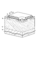
- a MOSFET having a planar structure has a first resistance type first base layer 12 having a high resistance and a first conductivity provided on the back surface of the first base layer 12, as shown in FIG.
- Type drain layer 10 second conductivity type second base layer 16 formed on the surface of first base layer 12, first conductivity type source layer 18 formed on the surface of second base layer 16,
- a gate insulating film 20 disposed on the surfaces of the source layer 18 and the second base layer 16, a gate electrode 22 disposed on the gate insulating film 20, and an interlayer insulating film 24 disposed on the gate electrode 22.
- the drain electrode provided on the drain layer 10 and the source electrode provided on the source layer 18 and the second base layer 16 are not shown in FIG.
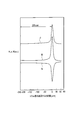
- FIG. 12 shows an example of a switching waveform of the semiconductor device according to the conventional example.
- a MOSFET having a super junction MOS structure exhibits superior performance in terms of switching loss and on-loss compared to a conventional planar structure MOSFET, but inferior in terms of through loss.
- the super junction MOSFET includes a column layer of the second conductivity type formed in the first base layer 12 below the second base layer 16 and the source layer 18 so as to face the drain layer 10. Therefore, the on-resistance is reduced, the gate sensitivity is increased, the gate charge amount Qg necessary for turn-on switching is reduced, and the turn-on switching time is shortened.
- the provision of this column layer increases the pn junction area, increases the reverse recovery time trr, and increases the turn-off switching time.
- the gate charge amount Qg is defined as, for example, the charge amount necessary for the gate-source voltage V GS to reach 10V.
- the reverse recovery time trr As a technique for shortening the reverse recovery time trr, there are a method using diffusion of heavy metal and a method of irradiating an electron beam. According to these methods, the reverse recovery time trr can be shortened, but there is a problem that the leakage current between the drain and the source increases because the controllability of trap level formation is poor.
- IGBT Insulated Gate Bipolar Transistor
- Japanese Patent Laid-Open No. 10-242165 (FIG. 1, pages 3-4) Japanese Patent Laid-Open No. 10-270451 (FIG. 1, page 4)
- An object of the present invention is to provide a semiconductor device having a super junction MOS structure that shortens the reverse recovery time trr without increasing the drain-source leakage current, and a method for manufacturing the same.
- a step of forming a first conductive type first base layer with high resistance a step of forming a first conductive type drain layer on the back surface of the first base layer, Forming a second conductivity type second base layer on the surface of the first base layer; forming a first conductivity type source layer on the surface of the second base layer; and Forming a gate insulating film on the surface of the base layer; forming a gate electrode on the gate insulating film; and draining the drain into the first base layer below the second base layer and the source layer.
- the present invention it is possible to provide a semiconductor device having a super junction MOS structure that shortens the reverse recovery time trr without increasing the drain-source leakage current and a method for manufacturing the same.
- FIG. 1 is a schematic sectional view of a semiconductor device according to a first embodiment of the present invention.
- 1 is a schematic bird's-eye view of a semiconductor device according to a first embodiment of the present invention.
- 1 is a schematic plan pattern configuration diagram of a semiconductor device according to a first embodiment of the present invention.
- FIG. FIG. 6 is another schematic planar pattern configuration diagram of the semiconductor device according to the first embodiment of the present invention. 6 is a switching waveform example of a comparative example of the semiconductor device according to the first embodiment of the present invention.
- FIG. 3 is a schematic cross-sectional structure diagram illustrating a relationship between an irradiation target position and a device structure when 3 He ++ ions are irradiated from the back surface to the semiconductor device according to the first embodiment of the present invention.
- FIG. 4 is a schematic diagram showing the relationship between the reverse recovery time trr, the drain-source saturation current I DSS, and the distance from the bottom surface of the column layer in the semiconductor device according to the first embodiment of the present invention.
- the typical bird's-eye view of the semiconductor device which concerns on a prior art example. 7 is a switching waveform example of a semiconductor device according to a conventional example.
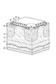
- FIG. 1 A schematic cross-sectional structure of the semiconductor device according to the first embodiment of the present invention is expressed as shown in FIG.
- FIG. 1 A schematic bird's-eye view structure of the semiconductor device according to the first embodiment is expressed as shown in FIG.
- the semiconductor device according to the first embodiment is provided on a first base layer 12 doped with n-type impurities with high resistance, and on the back surface of the first base layer 12, A drain layer 10 doped with an n-type impurity and a surface of the first base layer 12, a second base layer 16 doped with a p-type impurity and a surface of the second base layer 16, and an n-type impurity
- An interlayer insulating film 24 is disposed on the gate electrode 22. A broken line shown in FIG. 1
- heavy particles are irradiated to the column layer 14 to locally form trap levels.
- n-type impurity for example, P, As, Sb and the like
- p-type impurity for example, B, Al, Ga and the like
- impurities can be doped in each layer using a diffusion technique or an ion implantation technique.
- the gate insulating film 20 for example, a silicon oxide film, a silicon nitride film, a silicon oxynitride film, a hafnium oxide film, an alumina film, a tantalum oxide film, or the like can be applied.
- gate electrode 22 for example, polysilicon can be applied, and for the drain electrode 28 and the source electrode 26, for example, aluminum can be applied.
- interlayer insulating film 24 for example, a silicon oxide film, a silicon nitride film, a TEOS (tetraethoxysilane) film, or the like can be applied.
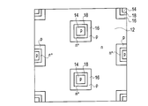
- the schematic planar pattern configuration of the semiconductor device according to the first embodiment shows an example in which a rectangular pattern is used as a base tone in the example of FIG.
- a rectangular pattern for example, as shown in FIG. 3, it may be arranged in a staggered pattern based on a rectangular pattern, or in a staggered pattern based on a hexagonal pattern as shown in FIG. You may arrange in a shape.
- the plane pattern configuration is not limited to a rectangle or a hexagon, but may be based on a circle, an ellipse, a pentagon, a polygon of a heptagon or more.
- 3 and 4 schematically show patterns of semiconductor layers such as the first base layer 12, the column layer 14, the second base layer 16, and the source layer 18, and the gate electrode 22, the source electrode 26, etc. The display is omitted.
- FIG. 5 shows an example of switching waveforms in a comparative example in which lifetime control by heavy particle irradiation is not performed in the semiconductor device according to the first embodiment.
- the reverse recovery time trr is 160 nsec, which is longer than 130 nsec of the conventional example shown in FIG.
- FIG. 6 shows a schematic cross-sectional structure for explaining the relationship between the irradiation target position and the device structure when the semiconductor device according to the first embodiment is irradiated with 3 He ++ ions from the back surface (IR: Irradiation). It is expressed as follows.
- WA the thickness of the drain layer 10 measured from the back surface of the semiconductor device.
- the coordinates are defined with the bottom surface of the column layer 14 as a reference, the direction of the source electrode 26 as the positive direction, and the direction of the drain layer 10 as the negative direction.
- the irradiation target position is defined as an attenuation peak position of the range of heavy particle ions irradiated from the back surface of the semiconductor device, and can be expressed on the above coordinates.
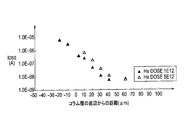
- FIG. 7 shows a case where the dose amount of 3 He ++ ions is 1 ⁇ 10 12 ions / cm 2 and 5 ⁇ 10 12 ions / cm 2 .
- the relationship between the reverse recovery time trr and the distance from the bottom surface of the column layer 14 corresponding to the attenuation peak position is expressed as shown in FIG. FIG. 8 also shows the case where the dose amount of 3 He ++ ions is 1 ⁇ 10 12 ions / cm 2 and 5 ⁇ 10 12 ions / cm 2 .
- the value of the drain-source saturation current I DSS tends to decrease as the distance from the bottom surface of the column layer 14 corresponding to the attenuation peak position increases.
- the reverse recovery time trr tends to increase as the distance from the bottom surface of the column layer 14 corresponding to the attenuation peak position increases.
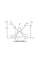
- the relationship between the reverse recovery time trr, the drain-source saturation current I DSS, and the distance from the bottom surface of the column layer 14 is schematically shown in FIG.
- the semiconductor device with reference to the bottom surface of the column layer 14, the first position PB obtained from the relationship between the distance from the bottom surface of the column layer 14 and the reverse recovery time trr, and the column layer 14
- the heavy particle irradiation so that the attenuation peak position of the heavy particle irradiation is included between the second position PA obtained from the relationship between the distance from the bottom surface of the electrode and the drain-source saturation current I DSS.
- a semiconductor device having a reverse recovery time trr shorter than the reverse recovery time t 0 and having a drain-source saturation current I DSS smaller than the drain-source saturation current I 0 can be obtained.
- a curve D has a reverse recovery time trr shorter than the reverse recovery time t 0 and a semiconductor device having a drain-source saturation current I DSS smaller than the drain-source saturation current I 0. Represents the attenuation peak curve of heavy particle irradiation.
- the first position PB is a heavy particle irradiation attenuation peak position corresponding to the reverse recovery time t 0 .
- the second position PA is the attenuation peak position of heavy particle irradiation corresponding to the drain-source saturation current I 0 .
- the reverse recovery time t 0 80 nsec and the drain-source saturation current I 0 is 1 ⁇ A
- the reverse recovery time trr ⁇ t 0 80 nsec
- the drain-source saturation current I DSS ⁇ I 0 1 ⁇ A
- the semiconductor device can be obtained.
- the particle species to be irradiated heavy particles for example, can be adopted proton, 3 the He ++, one of the 4 the He ++.
- the drain layer 10 made of a thin substrate.
- the dose amount of heavy particle irradiation can be set in the range of 5 ⁇ 10 10 to 5 ⁇ 10 12 particles / cm 2 , for example.
- FIG. 10 shows the relationship between the impurity density N, the resistivity ⁇ , the sheet resistance R, and the distance from the bottom surface of the column layer 14 in the semiconductor device according to the first embodiment.
- the resistivity ⁇ and the sheet resistance R show peak characteristics
- the impurity density N shows a decreasing peak characteristic.
- the method of manufacturing a semiconductor device includes a step of forming a first base layer 12 having a high resistance and a first conductivity type, Forming a drain layer 10 of the first conductivity type on the back surface, forming a second base layer 16 of the second conductivity type on the surface of the first base layer 12, and first on the surface of the second base layer 16.
- the step of locally forming the trap level uses the bottom surface of the column layer 14 as a reference, and sets the first position PB from the relationship between the distance from the bottom surface of the column layer 14 and the reverse recovery time trr.
- a step of determining, a step of determining the second position PA obtained from the relationship between the distance from the bottom surface of the column layer 14 and the drain-source saturation current I DSS, and the first position PB and the second position PA And a step of performing heavy particle irradiation so that an attenuation peak position is included in between.
- the first embodiment it is possible to improve the reverse recovery characteristics of the built-in diode while suppressing the deterioration of the drain-source saturation current I DSS and the gate-source threshold voltage. As a result, switching loss and diode reverse recovery loss can be reduced.
- the first embodiment it is possible to provide a semiconductor device having a super junction MOS structure that shortens the reverse recovery time trr without increasing the drain-source leakage current and a method for manufacturing the same.
- the semiconductor device of the present invention can be applied to a bridge circuit using a high voltage MOSFET, an LCD inverter, a motor, an automobile HID (High Intensity Discharge lamp) headlight lighting device, and the like.
Landscapes
- Insulated Gate Type Field-Effect Transistor (AREA)
- Thin Film Transistor (AREA)
- Chemical & Material Sciences (AREA)
- Composite Materials (AREA)
Abstract
Description
(素子構造)
本発明の第1の実施の形態に係る半導体装置の模式的断面構造は、図1に示すように表される。また、第1の実施の形態に係る半導体装置の模式的鳥瞰構造は、図2に示すように表される。
第1の実施の形態に係る半導体装置において、ドレイン・ソース間飽和電流IDSSと減衰ピーク位置に対応するコラム層14の底面からの距離との関係は、図7に示すように表される。図7においては、3He++イオンのドーズ量を1×10¹²個/cm2、5×1012個/cm2とした場合を示す。
第1の実施の形態に係る半導体装置の製造方法は、図1~図2に示すように、高抵抗で第1導電型の第1ベース層12を形成する工程と、第1ベース層12の裏面に第1導電型のドレイン層10を形成する工程と、第1ベース層12の表面に第2導電型の第2ベース層16を形成する工程と、第2ベース層16の表面に第1導電型のソース層18を形成する工程と、ソース層18および第2ベース層16の表面上にゲート絶縁膜20を形成する工程と、ゲート絶縁膜20上にゲート電極22を形成する工程と、第2ベース層16およびソース層18の下部の第1ベース層12内にドレイン層10に対向して第2導電型のコラム層14を形成する工程と、ドレイン層10にドレイン電極28を形成する工程と、
前記ソース層および前記第2ベース層にソース電極を形成する工程と、コラム層14に対して重粒子照射を行い、トラップレベルを局所的に形成する工程とを有する。
上記のように、本発明は第1の実施の形態によって記載したが、この開示の一部をなす論述および図面は例示的なものであり、この発明を限定するものであると理解すべきではない。この開示から当業者には様々な代替実施の形態、実施例および運用技術が明らかとなろう。
12…第1ベース層
14…コラム層
16…第2ベース層
18…ソース層
20…ゲート絶縁膜
22…ゲート電極
24…層間絶縁膜
26…ソース電極
28…ドレイン電極
Claims (9)
- 高抵抗で第1導電型の第1ベース層と、
前記第1ベース層の裏面に設けられた第1導電型のドレイン層と、
前記第1ベース層の表面に形成された第2導電型の第2ベース層と、
前記第2ベース層の表面に形成された第1導電型のソース層と、
前記ソース層および前記第2ベース層の表面上に配置されたゲート絶縁膜と、
前記ゲート絶縁膜上に配置されたゲート電極と、
前記第2ベース層および前記ソース層の下部の前記第1ベース層内に前記ドレイン層に対向して形成された第2導電型のコラム層と、
前記ドレイン層に設けられたドレイン電極と、
前記ソース層および前記第2ベース層に設けられたソース電極とを備え、
前記コラム層に対して重粒子照射を行い、トラップレベルを局所的に形成したことを特徴とする半導体装置。 - 前記コラム層の底面を基準とし、前記コラム層の底面からの距離と逆回復時間との関係より求めた第1の位置と、前記コラム層の底面からの距離とドレイン・ソース間飽和電流との関係より求めた第2の位置との間に、前記イオン照射の減衰ピーク位置が含まれることを特徴とする請求項1に記載の半導体装置。
- 前記重粒子照射する粒子種は、プロトン、3He++、4He++のいずれかであることを特徴とする請求項1または2に記載の半導体装置。
- 前記重粒子照射のドーズ量は、5×10¹⁰~5×10¹²個/cm2であることを特徴とする請求項1~3のいずれか1項に記載の半導体装置。
- 前記第1ベース層、前記第2ベース層、および前記ソース層は、矩形若しくは六角形を基調とする平面パターンを格子状、若しくは千鳥格子状に配置したことを特徴とする請求項1~4のいずれか1項に記載の半導体装置。
- 高抵抗で第1導電型の第1ベース層を形成する工程と、
前記第1ベース層の裏面に第1導電型のドレイン層を形成する工程と、
前記第1ベース層の表面に第2導電型の第2ベース層を形成する工程と、
前記第2ベース層の表面に第1導電型のソース層を形成する工程と、
前記ソース層および前記第2ベース層の表面上にゲート絶縁膜を形成する工程と、
前記ゲート絶縁膜上にゲート電極を形成する工程と、
前記第2ベース層および前記ソース層の下部の前記第1ベース層内に前記ドレイン層に対向して第2導電型のコラム層を形成する工程と、
前記ドレイン層にドレイン電極を形成する工程と、
前記ソース層および前記第2ベース層にソース電極を形成する工程と、
前記コラム層に対して重粒子照射を行い、トラップレベルを局所的に形成する工程と
を有することを特徴とする半導体装置の製造方法。 - 前記トラップレベルを局所的に形成する工程は、
前記コラム層の底面を基準とし、前記コラム層の底面からの距離と逆回復時間との関係より第1の位置を決定する工程と、
前記コラム層の底面からの距離とドレイン・ソース間飽和電流との関係より求めた第2の位置を決定する工程と、
前記第1の位置と前記第2の位置との間に減衰ピーク位置が含まれるように重粒子照射を実施する工程と
を有することを特徴とする請求項6に記載の半導体装置の製造方法。 - 前記重粒子照射する粒子種は、プロトン、3He++、4He++のいずれかであることを特徴とする請求項6または7に記載の半導体装置の製造方法。
- 前記重粒子照射のドーズ量は、5×10¹⁰~5×10¹²個/cm2であることを特徴とする請求項6~8のいずれか1項に記載の半導体装置の製造方法。
Priority Applications (9)
| Application Number | Priority Date | Filing Date | Title |
|---|---|---|---|
| US12/737,912 US8492829B2 (en) | 2008-09-01 | 2009-08-31 | Semiconductor device having super junction metal oxide semiconductor structure and fabrication method for the same |
| JP2010526808A JP5723595B2 (ja) | 2008-09-01 | 2009-08-31 | 半導体装置およびその製造方法 |
| EP09810077A EP2330617A4 (en) | 2008-09-01 | 2009-08-31 | SEMICONDUCTOR COMPONENT AND MANUFACTURING METHOD THEREFOR |
| CN200980133767.9A CN102138206B (zh) | 2008-09-01 | 2009-08-31 | 半导体装置及其制造方法 |
| US13/922,441 US8802548B2 (en) | 2008-09-01 | 2013-06-20 | Semiconductor device having super junction metal oxide semiconductor structure and fabrication method for the same |
| US14/320,671 US9385217B2 (en) | 2008-09-01 | 2014-07-01 | Semiconductor device having super junction metal oxide semiconductor structure and fabrication method for the same |
| US15/173,652 US9755065B2 (en) | 2008-09-01 | 2016-06-04 | Semiconductor device having super junction metal oxide semiconductor structure and fabrication method for the same |
| US15/677,003 US10217856B2 (en) | 2008-09-01 | 2017-08-14 | Semiconductor device having super junction metal oxide semiconductor structure and fabrication method for the same |
| US16/245,681 US10672900B2 (en) | 2008-09-01 | 2019-01-11 | Semiconductor device having super junction metal oxide semiconductor structure and fabrication method for the same |
Applications Claiming Priority (2)
| Application Number | Priority Date | Filing Date | Title |
|---|---|---|---|
| JP2008-223370 | 2008-09-01 | ||
| JP2008223370 | 2008-09-01 |
Related Child Applications (2)
| Application Number | Title | Priority Date | Filing Date |
|---|---|---|---|
| US12/737,912 A-371-Of-International US8492829B2 (en) | 2008-09-01 | 2009-08-31 | Semiconductor device having super junction metal oxide semiconductor structure and fabrication method for the same |
| US13/922,441 Division US8802548B2 (en) | 2008-09-01 | 2013-06-20 | Semiconductor device having super junction metal oxide semiconductor structure and fabrication method for the same |
Publications (1)
| Publication Number | Publication Date |
|---|---|
| WO2010024433A1 true WO2010024433A1 (ja) | 2010-03-04 |
Family
ID=41721592
Family Applications (1)
| Application Number | Title | Priority Date | Filing Date |
|---|---|---|---|
| PCT/JP2009/065171 Ceased WO2010024433A1 (ja) | 2008-09-01 | 2009-08-31 | 半導体装置およびその製造方法 |
Country Status (7)
| Country | Link |
|---|---|
| US (6) | US8492829B2 (ja) |
| EP (1) | EP2330617A4 (ja) |
| JP (4) | JP5723595B2 (ja) |
| KR (1) | KR101614565B1 (ja) |
| CN (1) | CN102138206B (ja) |
| TW (1) | TWI470799B (ja) |
| WO (1) | WO2010024433A1 (ja) |
Cited By (16)
| Publication number | Priority date | Publication date | Assignee | Title |
|---|---|---|---|---|
| JP2012142330A (ja) * | 2010-12-28 | 2012-07-26 | Rohm Co Ltd | 半導体装置およびその製造方法 |
| JP2013102111A (ja) * | 2011-10-17 | 2013-05-23 | Rohm Co Ltd | 半導体装置およびその製造方法 |
| US9048250B2 (en) | 2013-02-25 | 2015-06-02 | Fuji Electric Co., Ltd. | Method of manufacturing a super-junction semiconductor device |
| JP2015135987A (ja) * | 2008-09-01 | 2015-07-27 | ローム株式会社 | 半導体装置およびその製造方法 |
| US9219141B2 (en) | 2013-07-10 | 2015-12-22 | Fuji Electric Co., Ltd. | Super junction MOSFET, method of manufacturing the same, and complex semiconductor device |
| JP2017055465A (ja) * | 2015-09-07 | 2017-03-16 | ジョンソンコントロールズ ヒタチ エア コンディショニング テクノロジー(ホンコン)リミテッド | 直流電源装置及びこれを搭載した空気調和機 |
| US9711634B2 (en) | 2013-09-18 | 2017-07-18 | Fuji Electric Co., Ltd. | Semiconductor device including a super junction MOSFET |
| JP2017183419A (ja) * | 2016-03-29 | 2017-10-05 | ローム株式会社 | 半導体装置 |
| US9887279B2 (en) | 2015-09-15 | 2018-02-06 | Rohm Co., Ltd. | Semiconductor device and inverter including the semiconductor device |
| WO2019087424A1 (ja) * | 2017-11-01 | 2019-05-09 | 新電元工業株式会社 | 半導体装置及び半導体装置の製造方法 |
| JP6530867B1 (ja) * | 2017-12-27 | 2019-06-12 | 新電元工業株式会社 | Mosfet、mosfetの製造方法及び電力変換回路 |
| JP2020025459A (ja) * | 2019-10-16 | 2020-02-13 | 日立ジョンソンコントロールズ空調株式会社 | 直流電源装置及びこれを搭載した空気調和機 |
| US10720525B2 (en) | 2018-03-29 | 2020-07-21 | Rohm Co., Ltd. | Semiconductor device |
| US11127850B2 (en) | 2017-01-27 | 2021-09-21 | Rohm Co., Ltd. | Semiconductor device |
| JP2022069673A (ja) * | 2016-06-28 | 2022-05-11 | 日立ジョンソンコントロールズ空調株式会社 | 電力変換装置、及びこれを備える空気調和機 |
| JP2022132507A (ja) * | 2019-10-16 | 2022-09-08 | 日立ジョンソンコントロールズ空調株式会社 | 直流電源装置及びこれを搭載した空気調和機 |
Families Citing this family (7)
| Publication number | Priority date | Publication date | Assignee | Title |
|---|---|---|---|---|
| JP5586546B2 (ja) * | 2011-03-23 | 2014-09-10 | 株式会社東芝 | 半導体装置 |
| CN103325825B (zh) * | 2012-03-20 | 2016-01-27 | 宁波敏泰光电科技有限公司 | 超结mosfet |
| JP6263966B2 (ja) | 2012-12-12 | 2018-01-24 | 富士電機株式会社 | 半導体装置 |
| US9472456B2 (en) * | 2013-12-24 | 2016-10-18 | Intel Corporation | Technology for selectively etching titanium and titanium nitride in the presence of other materials |
| CN105161491B (zh) * | 2015-09-22 | 2019-03-15 | 苏州东微半导体有限公司 | 一种集成栅极驱动功率器件及其制备方法 |
| CN106887464B (zh) * | 2017-01-04 | 2019-12-06 | 上海华虹宏力半导体制造有限公司 | 超结器件及其制造方法 |
| US10186586B1 (en) * | 2017-09-26 | 2019-01-22 | Sanken Electric Co., Ltd. | Semiconductor device and method for forming the semiconductor device |
Citations (10)
| Publication number | Priority date | Publication date | Assignee | Title |
|---|---|---|---|---|
| JPS62219664A (ja) * | 1986-03-20 | 1987-09-26 | Hitachi Ltd | Mos型半導体素子の製造方法 |
| JPS62298120A (ja) * | 1986-06-18 | 1987-12-25 | Hitachi Ltd | 半導体装置およびその製造方法 |
| JPS63115383A (ja) * | 1986-11-04 | 1988-05-19 | Matsushita Electronics Corp | 電界効果トランジスタの製造方法 |
| JPH03263376A (ja) * | 1990-03-13 | 1991-11-22 | Mitsubishi Electric Corp | 電界効果型半導体装置 |
| JPH10150208A (ja) * | 1996-11-15 | 1998-06-02 | Toshiba Corp | 半導体装置の製造方法 |
| JPH10242165A (ja) | 1997-02-28 | 1998-09-11 | Hitachi Ltd | 半導体スイッチング素子及びそれを用いた電力変換装置並びに半導体スイッチング素子の駆動方法 |
| JPH10270451A (ja) | 1997-03-25 | 1998-10-09 | Rohm Co Ltd | 半導体装置およびその製造方法 |
| JP2001102577A (ja) * | 1999-09-30 | 2001-04-13 | Toshiba Corp | 半導体装置 |
| JP2004022716A (ja) * | 2002-06-14 | 2004-01-22 | Fuji Electric Holdings Co Ltd | 半導体素子 |
| JP2005197497A (ja) * | 2004-01-08 | 2005-07-21 | Toyota Central Res & Dev Lab Inc | 半導体装置 |
Family Cites Families (38)
| Publication number | Priority date | Publication date | Assignee | Title |
|---|---|---|---|---|
| US4053925A (en) * | 1975-08-07 | 1977-10-11 | Ibm Corporation | Method and structure for controllng carrier lifetime in semiconductor devices |
| US4762802A (en) * | 1984-11-09 | 1988-08-09 | American Telephone And Telegraph Company At&T, Bell Laboratories | Method for preventing latchup in CMOS devices |
| JP3034895B2 (ja) | 1990-03-08 | 2000-04-17 | 株式会社日立製作所 | 電力変換器システム |
| JPH03259537A (ja) * | 1990-03-09 | 1991-11-19 | Hitachi Ltd | 半導体装置及びその製法 |
| JP3081739B2 (ja) * | 1992-10-20 | 2000-08-28 | 三菱電機株式会社 | 絶縁ゲート型半導体装置及びその製造方法 |
| EP0694960B1 (en) * | 1994-07-25 | 2002-07-03 | Consorzio per la Ricerca sulla Microelettronica nel Mezzogiorno - CoRiMMe | Process for the localized reduction of the lifetime of charge carriers |
| JP3259537B2 (ja) | 1994-08-29 | 2002-02-25 | 松下電器産業株式会社 | 半導体装置の製造方法 |
| JP2883017B2 (ja) * | 1995-02-20 | 1999-04-19 | ローム株式会社 | 半導体装置およびその製法 |
| JPH09121052A (ja) | 1995-08-21 | 1997-05-06 | Fuji Electric Co Ltd | 半導体装置およびその製造方法 |
| US5759904A (en) * | 1996-11-06 | 1998-06-02 | Southwest Research Institute | Suppression of transient enhanced diffusion in ion implanted silicon |
| DE19730759C1 (de) * | 1997-07-17 | 1998-09-03 | Siemens Ag | Vertikaler Leistungs-MOSFET |
| DE19830332C2 (de) * | 1998-07-07 | 2003-04-17 | Infineon Technologies Ag | Vertikales Halbleiterbauelement mit reduziertem elektrischem Oberflächenfeld |
| JP4653273B2 (ja) * | 1999-11-05 | 2011-03-16 | 富士電機システムズ株式会社 | 半導体装置、および、その製造方法 |
| US6709955B2 (en) * | 2000-04-17 | 2004-03-23 | Stmicroelectronics S.R.L. | Method of fabricating electronic devices integrated in semiconductor substrates provided with gettering sites, and a device fabricated by the method |
| US6509240B2 (en) * | 2000-05-15 | 2003-01-21 | International Rectifier Corporation | Angle implant process for cellular deep trench sidewall doping |
| JP2002093813A (ja) * | 2000-09-13 | 2002-03-29 | Toyota Motor Corp | 半導体装置の製造方法 |
| DE10120656C2 (de) * | 2001-04-27 | 2003-07-10 | Infineon Technologies Ag | Halbleiterbauelement mit erhöhter Avalanche-Festigkeit |
| JP2003101022A (ja) | 2001-09-27 | 2003-04-04 | Toshiba Corp | 電力用半導体素子 |
| DE10137676B4 (de) * | 2001-08-01 | 2007-08-23 | Infineon Technologies Ag | ZVS-Brückenschaltung zum entlasteten Schalten |
| US20030030051A1 (en) * | 2001-08-09 | 2003-02-13 | International Rectifier Corporation | Superjunction device with improved avalanche capability and breakdown voltage |
| US6686244B2 (en) * | 2002-03-21 | 2004-02-03 | General Semiconductor, Inc. | Power semiconductor device having a voltage sustaining region that includes doped columns formed with a single ion implantation step |
| JP3952452B2 (ja) * | 2002-03-25 | 2007-08-01 | 新電元工業株式会社 | 半導体装置の製造方法 |
| JP3979258B2 (ja) * | 2002-05-21 | 2007-09-19 | 富士電機デバイステクノロジー株式会社 | Mis半導体装置およびその製造方法 |
| DE10243758A1 (de) * | 2002-09-20 | 2004-04-01 | eupec Europäische Gesellschaft für Leistungshalbleiter mbH | Verfahren zur Herstellung einer vergrabenen Stoppzone in einem Halbleiterbauelement und Halbleiterbauelement mit einer vergrabenen Stoppzone |
| US6838321B2 (en) * | 2002-09-26 | 2005-01-04 | Mitsubishi Denki Kabushiki Kaisha | Semiconductor substrate with defects reduced or removed and method of manufacturing the same, and semiconductor device capable of bidirectionally retaining breakdown voltage and method of manufacturing the same |
| US7166890B2 (en) * | 2003-10-21 | 2007-01-23 | Srikant Sridevan | Superjunction device with improved ruggedness |
| JP4832731B2 (ja) | 2004-07-07 | 2011-12-07 | 株式会社東芝 | 電力用半導体装置 |
| JP4843253B2 (ja) * | 2005-05-23 | 2011-12-21 | 株式会社東芝 | 電力用半導体装置 |
| JP4996848B2 (ja) | 2005-11-30 | 2012-08-08 | 株式会社東芝 | 半導体装置 |
| EP2058846B1 (de) * | 2006-01-20 | 2011-08-31 | Infineon Technologies Austria AG | Verfahren zur Herstellung einer n-dotierten Zone in einem Halbleiterwafer und Halbleiterbauelement |
| JP2008124300A (ja) | 2006-11-14 | 2008-05-29 | Rohm Co Ltd | 半導体装置およびこれを用いた電気回路 |
| JP4412344B2 (ja) * | 2007-04-03 | 2010-02-10 | 株式会社デンソー | 半導体装置およびその製造方法 |
| DE102007022533B4 (de) * | 2007-05-14 | 2014-04-30 | Infineon Technologies Ag | Verfahren zum Herstellen eines Halbleiterelements und Halbleiterelement |
| WO2010024433A1 (ja) | 2008-09-01 | 2010-03-04 | ローム株式会社 | 半導体装置およびその製造方法 |
| JP5748476B2 (ja) * | 2010-12-28 | 2015-07-15 | ローム株式会社 | 半導体装置およびその製造方法 |
| JP6135178B2 (ja) * | 2013-02-25 | 2017-05-31 | 富士電機株式会社 | 超接合半導体装置の製造方法 |
| JP6234696B2 (ja) * | 2013-04-16 | 2017-11-22 | ローム株式会社 | 半導体装置 |
| JP6611532B2 (ja) * | 2015-09-17 | 2019-11-27 | ローム株式会社 | 半導体装置および半導体装置の製造方法 |
-
2009
- 2009-08-31 WO PCT/JP2009/065171 patent/WO2010024433A1/ja not_active Ceased
- 2009-08-31 CN CN200980133767.9A patent/CN102138206B/zh active Active
- 2009-08-31 KR KR1020117007467A patent/KR101614565B1/ko not_active Expired - Fee Related
- 2009-08-31 JP JP2010526808A patent/JP5723595B2/ja active Active
- 2009-08-31 EP EP09810077A patent/EP2330617A4/en not_active Withdrawn
- 2009-08-31 US US12/737,912 patent/US8492829B2/en active Active
- 2009-09-01 TW TW98129401A patent/TWI470799B/zh not_active IP Right Cessation
-
2013
- 2013-06-20 US US13/922,441 patent/US8802548B2/en active Active
-
2014
- 2014-07-01 US US14/320,671 patent/US9385217B2/en active Active
-
2015
- 2015-03-24 JP JP2015061288A patent/JP6243370B2/ja active Active
-
2016
- 2016-06-04 US US15/173,652 patent/US9755065B2/en active Active
-
2017
- 2017-08-14 US US15/677,003 patent/US10217856B2/en active Active
- 2017-09-01 JP JP2017168375A patent/JP6557304B2/ja active Active
-
2019
- 2019-01-11 US US16/245,681 patent/US10672900B2/en active Active
- 2019-06-11 JP JP2019108642A patent/JP6731522B2/ja active Active
Patent Citations (10)
| Publication number | Priority date | Publication date | Assignee | Title |
|---|---|---|---|---|
| JPS62219664A (ja) * | 1986-03-20 | 1987-09-26 | Hitachi Ltd | Mos型半導体素子の製造方法 |
| JPS62298120A (ja) * | 1986-06-18 | 1987-12-25 | Hitachi Ltd | 半導体装置およびその製造方法 |
| JPS63115383A (ja) * | 1986-11-04 | 1988-05-19 | Matsushita Electronics Corp | 電界効果トランジスタの製造方法 |
| JPH03263376A (ja) * | 1990-03-13 | 1991-11-22 | Mitsubishi Electric Corp | 電界効果型半導体装置 |
| JPH10150208A (ja) * | 1996-11-15 | 1998-06-02 | Toshiba Corp | 半導体装置の製造方法 |
| JPH10242165A (ja) | 1997-02-28 | 1998-09-11 | Hitachi Ltd | 半導体スイッチング素子及びそれを用いた電力変換装置並びに半導体スイッチング素子の駆動方法 |
| JPH10270451A (ja) | 1997-03-25 | 1998-10-09 | Rohm Co Ltd | 半導体装置およびその製造方法 |
| JP2001102577A (ja) * | 1999-09-30 | 2001-04-13 | Toshiba Corp | 半導体装置 |
| JP2004022716A (ja) * | 2002-06-14 | 2004-01-22 | Fuji Electric Holdings Co Ltd | 半導体素子 |
| JP2005197497A (ja) * | 2004-01-08 | 2005-07-21 | Toyota Central Res & Dev Lab Inc | 半導体装置 |
Non-Patent Citations (1)
| Title |
|---|
| See also references of EP2330617A4 |
Cited By (30)
| Publication number | Priority date | Publication date | Assignee | Title |
|---|---|---|---|---|
| JP2015135987A (ja) * | 2008-09-01 | 2015-07-27 | ローム株式会社 | 半導体装置およびその製造方法 |
| US9755065B2 (en) | 2008-09-01 | 2017-09-05 | Rohm Co., Ltd. | Semiconductor device having super junction metal oxide semiconductor structure and fabrication method for the same |
| US10217856B2 (en) | 2008-09-01 | 2019-02-26 | Rohm Co., Ltd. | Semiconductor device having super junction metal oxide semiconductor structure and fabrication method for the same |
| US10672900B2 (en) | 2008-09-01 | 2020-06-02 | Rohm Co., Ltd. | Semiconductor device having super junction metal oxide semiconductor structure and fabrication method for the same |
| US9536948B2 (en) | 2010-12-28 | 2017-01-03 | Rohm Co., Ltd. | Semiconductor device, method of manufacturing the same, and power module |
| US9087857B2 (en) | 2010-12-28 | 2015-07-21 | Rohm Co., Ltd. | Semiconductor device, method of manufacturing the same, and power module |
| US9184231B2 (en) | 2010-12-28 | 2015-11-10 | Rohm Co., Ltd. | Semiconductor device, method of manufacturing the same, and power module |
| US9306000B2 (en) | 2010-12-28 | 2016-04-05 | Rohm Co., Ltd. | Semiconductor device, method of manufacturing the same, and power module |
| JP2012142330A (ja) * | 2010-12-28 | 2012-07-26 | Rohm Co Ltd | 半導体装置およびその製造方法 |
| US8921925B2 (en) | 2010-12-28 | 2014-12-30 | Rohm Co., Ltd. | Semiconductor device, method of manufacturing the same, and power module |
| JP2013102111A (ja) * | 2011-10-17 | 2013-05-23 | Rohm Co Ltd | 半導体装置およびその製造方法 |
| US9048250B2 (en) | 2013-02-25 | 2015-06-02 | Fuji Electric Co., Ltd. | Method of manufacturing a super-junction semiconductor device |
| US9219141B2 (en) | 2013-07-10 | 2015-12-22 | Fuji Electric Co., Ltd. | Super junction MOSFET, method of manufacturing the same, and complex semiconductor device |
| TWI608618B (zh) * | 2013-09-18 | 2017-12-11 | 富士電機股份有限公司 | Semiconductor device and its manufacturing method |
| US9954078B2 (en) | 2013-09-18 | 2018-04-24 | Fuji Electric Co., Ltd. | Method for manufacturing a semiconductor device having a super junction MOSFET |
| US9711634B2 (en) | 2013-09-18 | 2017-07-18 | Fuji Electric Co., Ltd. | Semiconductor device including a super junction MOSFET |
| JP2017055465A (ja) * | 2015-09-07 | 2017-03-16 | ジョンソンコントロールズ ヒタチ エア コンディショニング テクノロジー(ホンコン)リミテッド | 直流電源装置及びこれを搭載した空気調和機 |
| US9887279B2 (en) | 2015-09-15 | 2018-02-06 | Rohm Co., Ltd. | Semiconductor device and inverter including the semiconductor device |
| JP2017183419A (ja) * | 2016-03-29 | 2017-10-05 | ローム株式会社 | 半導体装置 |
| JP2022069673A (ja) * | 2016-06-28 | 2022-05-11 | 日立ジョンソンコントロールズ空調株式会社 | 電力変換装置、及びこれを備える空気調和機 |
| US11127850B2 (en) | 2017-01-27 | 2021-09-21 | Rohm Co., Ltd. | Semiconductor device |
| WO2019087424A1 (ja) * | 2017-11-01 | 2019-05-09 | 新電元工業株式会社 | 半導体装置及び半導体装置の製造方法 |
| WO2019087341A1 (ja) * | 2017-11-01 | 2019-05-09 | 新電元工業株式会社 | 半導体装置及び半導体装置の製造方法 |
| JPWO2019087424A1 (ja) * | 2017-11-01 | 2020-01-16 | 新電元工業株式会社 | 半導体装置及び半導体装置の製造方法 |
| US10818496B2 (en) | 2017-11-01 | 2020-10-27 | Shindengen Electric Manufacturing Co., Ltd. | Semiconductor device having crystal defects and method of manufacturing the semiconductor device having crystal defects |
| JP6530867B1 (ja) * | 2017-12-27 | 2019-06-12 | 新電元工業株式会社 | Mosfet、mosfetの製造方法及び電力変換回路 |
| US10720525B2 (en) | 2018-03-29 | 2020-07-21 | Rohm Co., Ltd. | Semiconductor device |
| JP2020025459A (ja) * | 2019-10-16 | 2020-02-13 | 日立ジョンソンコントロールズ空調株式会社 | 直流電源装置及びこれを搭載した空気調和機 |
| JP2021121168A (ja) * | 2019-10-16 | 2021-08-19 | 日立ジョンソンコントロールズ空調株式会社 | 直流電源装置及びこれを搭載した空気調和機 |
| JP2022132507A (ja) * | 2019-10-16 | 2022-09-08 | 日立ジョンソンコントロールズ空調株式会社 | 直流電源装置及びこれを搭載した空気調和機 |
Also Published As
| Publication number | Publication date |
|---|---|
| JP2017228793A (ja) | 2017-12-28 |
| US20160284835A1 (en) | 2016-09-29 |
| KR101614565B1 (ko) | 2016-04-21 |
| TWI470799B (zh) | 2015-01-21 |
| CN102138206A (zh) | 2011-07-27 |
| US20130302957A1 (en) | 2013-11-14 |
| US8492829B2 (en) | 2013-07-23 |
| US9755065B2 (en) | 2017-09-05 |
| EP2330617A1 (en) | 2011-06-08 |
| KR20110069039A (ko) | 2011-06-22 |
| JP6557304B2 (ja) | 2019-08-07 |
| JP5723595B2 (ja) | 2015-05-27 |
| JP6731522B2 (ja) | 2020-07-29 |
| US20190148536A1 (en) | 2019-05-16 |
| TW201011917A (en) | 2010-03-16 |
| US8802548B2 (en) | 2014-08-12 |
| US10672900B2 (en) | 2020-06-02 |
| JP6243370B2 (ja) | 2017-12-06 |
| US20180012987A1 (en) | 2018-01-11 |
| US9385217B2 (en) | 2016-07-05 |
| JPWO2010024433A1 (ja) | 2012-01-26 |
| US10217856B2 (en) | 2019-02-26 |
| JP2015135987A (ja) | 2015-07-27 |
| US20110147829A1 (en) | 2011-06-23 |
| CN102138206B (zh) | 2014-03-12 |
| US20140312411A1 (en) | 2014-10-23 |
| JP2019145849A (ja) | 2019-08-29 |
| EP2330617A4 (en) | 2012-01-25 |
Similar Documents
| Publication | Publication Date | Title |
|---|---|---|
| JP6731522B2 (ja) | 半導体装置およびその製造方法 | |
| US6246092B1 (en) | High breakdown voltage MOS semiconductor apparatus | |
| KR100244282B1 (ko) | 고전압 트랜지스터의 구조 및 제조 방법 | |
| US20140209972A1 (en) | Semiconductor device | |
| US8294206B2 (en) | Integrated circuit device and method for its production | |
| US9219138B2 (en) | Semiconductor device having localized charge balance structure and method | |
| CN107949916A (zh) | 半导体元件 | |
| CN1377093A (zh) | 高耐压半导体器件 | |
| WO2013058191A1 (ja) | 半導体装置およびその製造方法 | |
| JP2005510061A (ja) | トレンチ・ゲート半導体装置とその製造方法 | |
| JP4840551B2 (ja) | Mosトランジスタ | |
| JP2001135831A (ja) | 半導体装置 | |
| JP5003598B2 (ja) | 半導体装置 | |
| KR100290913B1 (ko) | 고전압 소자 및 그 제조방법 | |
| US20230146397A1 (en) | Semiconductor device | |
| JP2024039276A (ja) | 半導体装置、および、半導体装置の製造方法 | |
| JP2007134421A (ja) | パワーmosfet、igbtなどの縦型半導体装置とその製造方法 |
Legal Events
| Date | Code | Title | Description |
|---|---|---|---|
| WWE | Wipo information: entry into national phase |
Ref document number: 200980133767.9 Country of ref document: CN |
|
| 121 | Ep: the epo has been informed by wipo that ep was designated in this application |
Ref document number: 09810077 Country of ref document: EP Kind code of ref document: A1 |
|
| WWE | Wipo information: entry into national phase |
Ref document number: 2010526808 Country of ref document: JP |
|
| WWE | Wipo information: entry into national phase |
Ref document number: 12737912 Country of ref document: US |
|
| NENP | Non-entry into the national phase |
Ref country code: DE |
|
| WWE | Wipo information: entry into national phase |
Ref document number: 2009810077 Country of ref document: EP |
|
| ENP | Entry into the national phase |
Ref document number: 20117007467 Country of ref document: KR Kind code of ref document: A |