WO2010044193A1 - Procédé d’analyse d’échantillon - Google Patents
Procédé d’analyse d’échantillon Download PDFInfo
- Publication number
- WO2010044193A1 WO2010044193A1 PCT/JP2009/004735 JP2009004735W WO2010044193A1 WO 2010044193 A1 WO2010044193 A1 WO 2010044193A1 JP 2009004735 W JP2009004735 W JP 2009004735W WO 2010044193 A1 WO2010044193 A1 WO 2010044193A1
- Authority
- WO
- WIPO (PCT)
- Prior art keywords
- sample
- wave
- interface
- analysis method
- incident
- Prior art date
- Legal status (The legal status is an assumption and is not a legal conclusion. Google has not performed a legal analysis and makes no representation as to the accuracy of the status listed.)
- Ceased
Links
Images




Classifications
-
- G—PHYSICS
- G01—MEASURING; TESTING
- G01N—INVESTIGATING OR ANALYSING MATERIALS BY DETERMINING THEIR CHEMICAL OR PHYSICAL PROPERTIES
- G01N21/00—Investigating or analysing materials by the use of optical means, i.e. using sub-millimetre waves, infrared, visible or ultraviolet light
- G01N21/17—Systems in which incident light is modified in accordance with the properties of the material investigated
- G01N21/25—Colour; Spectral properties, i.e. comparison of effect of material on the light at two or more different wavelengths or wavelength bands
- G01N21/31—Investigating relative effect of material at wavelengths characteristic of specific elements or molecules, e.g. atomic absorption spectrometry
- G01N21/35—Investigating relative effect of material at wavelengths characteristic of specific elements or molecules, e.g. atomic absorption spectrometry using infrared light
- G01N21/3581—Investigating relative effect of material at wavelengths characteristic of specific elements or molecules, e.g. atomic absorption spectrometry using infrared light using far infrared light; using Terahertz radiation
-
- G—PHYSICS
- G01—MEASURING; TESTING
- G01N—INVESTIGATING OR ANALYSING MATERIALS BY DETERMINING THEIR CHEMICAL OR PHYSICAL PROPERTIES
- G01N21/00—Investigating or analysing materials by the use of optical means, i.e. using sub-millimetre waves, infrared, visible or ultraviolet light
- G01N21/17—Systems in which incident light is modified in accordance with the properties of the material investigated
- G01N21/25—Colour; Spectral properties, i.e. comparison of effect of material on the light at two or more different wavelengths or wavelength bands
- G01N21/31—Investigating relative effect of material at wavelengths characteristic of specific elements or molecules, e.g. atomic absorption spectrometry
- G01N21/35—Investigating relative effect of material at wavelengths characteristic of specific elements or molecules, e.g. atomic absorption spectrometry using infrared light
- G01N21/3563—Investigating relative effect of material at wavelengths characteristic of specific elements or molecules, e.g. atomic absorption spectrometry using infrared light for analysing solids; Preparation of samples therefor
Definitions
- the present invention relates to a technique for analyzing a sample using terahertz waves.
- a terahertz wave refers to an electromagnetic wave having a frequency of 20 GHz to 120 THz. Examples of analysis include measuring physical properties and dimensions of the sample itself, and measuring the amount of biopolymer attached to the sample.
- a measurement result corresponding to the physical property of the sample is obtained. For example, if a sample is irradiated with terahertz waves of different wavelengths, the terahertz wave of a specific wavelength is absorbed by the electromagnetic wave absorption of the sample, so the frequency characteristic of the terahertz wave transmittance is a unique waveform corresponding to the physical properties of the sample Appears as
- THz-TDS terahertz time domain spectroscopy
- Example 2 of Patent Document 1 THz-TDS by a reflective optical system is shown.
- the terahertz wave emitted from the terahertz wave generator is focused and irradiated on the sample through a parabolic mirror, and then the terahertz wave reflected on the sample is reflected using the parabolic mirror. Condensed on the detector.
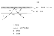
- FIG. 11 was created by the applicant based on the description in Patent Document 1.
- the conventional sample holder 100 includes a sample 102 to be measured and a metal film 101 in contact with the sample 102.
- the metal film 101 is a mirror that reflects almost 100% of the terahertz wave.
- the sample 102 In order to measure the transmittance of the sample 102 with respect to the terahertz wave, the sample 102 is irradiated with the terahertz wave.
- the terahertz wave propagation path in the sample at that time will be described with reference to FIG.
- an irradiation wave I that is a terahertz wave is incident on the sample 102.
- a part of the irradiation wave I becomes a reflected wave R 0 that directly hits and reflects the sample 102, and the other part becomes an in-sample propagation wave r 0 that passes through the sample 102.
- the reflected wave R 0 and the propagation wave r 0 in the sample are refracted due to the difference in permittivity between the atmosphere and the sample 102.
- Samples in propagating wave r 0 is reflected by the metal film 101, the sample in the propagating wave r 1, and the further surface in reflected sample the propagating wave r 2 next to the part of the sample 102 air samples in propagating wave r 1 The remaining part passes through the interface and is emitted to become an outgoing wave R 1 .
- the magnitudes of the amplitudes of the reflected wave R 0 and the outgoing wave R 1 are obtained on the time axis, and Fourier transform is performed to obtain the composition, physical properties, and mass of the sample 102.
- This is the conventional THz-TDS.
- the terahertz wave is not sufficiently absorbed in the sample, and the difference in amplitude between the reflected wave R 0 and the output wave R 1 does not change between when the sample is present and when the sample is present, and sufficient analysis of the sample 102 is performed.
- the transmission path of the terahertz wave itself is shortened, and a situation where electromagnetic wave absorption is not sufficiently performed occurs.
- the electromagnetic wave is not sufficiently absorbed, and it is impossible to measure the minute amount of 1 mg or less by the conventional method.
- the problem to be solved by the present invention is to accurately measure the composition, physical properties, mass, and dimensions of a micro sample, a micro sample, or a thin layer sample.
- the sample analysis method is a sample analysis method for analyzing a sample that is permeable to terahertz waves, and a reflecting member is provided in contact with the first main surface side of the sample.
- An incident member is provided in contact with the second main surface side of the first member, and the sample is irradiated with terahertz waves from the outside of the incident member toward the sample, and the second main surface side is irradiated with a terahertz wave.
- the sample is analyzed using an interference wave generated by a single-surface reflected wave and a second-surface reflected wave at the interface between the second main surface of the sample and the incident member.
- a terahertz wave refers to an electromagnetic wave having a frequency of 20 GHz to 120 THz.
- the interface between the first main surface of the sample and the reflecting member and the interface between the second main surface of the sample and the incident member are parallel.
- the interference wave includes an outgoing wave emitted from the first surface reflected wave through the sample and the incident member, and an incident member from the second surface reflected wave. And an outgoing wave that has passed through and emitted.
- the interference wave is in an interface between the first main surface of the sample and the reflecting member, and an interface between the second main surface of the sample and the incident member.
- a terahertz wave is formed from multiple reflected waves that are reflected multiple times. Multiple reflected waves are reflected waves that are reflected multiple times at the interface between the sample and the reflecting member and at the interface between the sample and the incident member in the process from irradiating the sample with the terahertz wave until it is emitted.
- the refractive index of the reflecting member is larger than the refractive index of the sample
- the refractive index of the incident member is larger than the refractive index of the sample
- the refractive index of the incident member is the incident light. It is larger than the refractive index of the atmosphere existing outside the member.
- a terahertz wave reflection suppressing layer is provided in contact with the outside of the incident member.
- the sample analysis method is a sample analysis method when the sample is formed of a plurality of layers having different dielectric constants, and is an analysis target of the plurality of layers of the sample.
- the layer is brought into contact with the reflective member and the sample is analyzed.
- a sample analysis method is a sample analysis method for analyzing a sample having permeability to terahertz waves, and a reflective member is applied to the first main surface side of the sample.
- An entrance member is provided in contact with the second main surface side of the sample, and a terahertz wave is irradiated from the outside of the entrance member toward the sample, and the first main surface of the sample and the reflection are irradiated.
- the outgoing wave finally emitted to the outside means a terahertz wave that has been emitted to the outside after being propagated through the sample or the incident member, whether once or plural times. .
- sample analysis method of the present invention it is possible to accurately measure the composition, physical properties, mass, and dimensions of a minute sample, a minute sample, or a thin layer sample.
- FIG. 1 is a diagram illustrating a sample holding unit and a terahertz wave propagation path in the sample holding unit in the embodiment.
- FIG. 2 is a diagram illustrating the entire THz-TDS imaging apparatus according to the first embodiment.
- FIG. 3 is a diagram illustrating a specific structure of the sample holder in the first embodiment.
- FIG. 4A is a diagram showing a time waveform by THz-TDS in Example 1
- FIG. 4B is a diagram showing a terahertz wave propagation path in the sample holding unit and the sample holding unit in Example 1. It is.
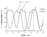
- FIG. 5 is a diagram illustrating frequency characteristics of transmittance according to the first embodiment.
- FIG. 6A is a diagram illustrating the sample holding unit 40 of the present embodiment, and FIG.
- FIG. 6B is an enlarged view of a portion A in FIG.
- FIG. 7 is a view showing a sample holder in the third embodiment.
- FIG. 8 is a schematic diagram of a biotin membrane array in Example 4 and a fluorescence detection image as a comparative example.
- FIG. 9 is a detection image of streptavidin on the biotin membrane array in Example 4.
- FIG. 10 is a detection image of lectins on the sugar chain membrane array in Example 5.
- FIG. 11 is a diagram for explaining a sample holder and a terahertz wave propagation path in a conventional THz-TDS.
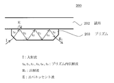
- FIG. 12 is a diagram showing a sample holder and a terahertz propagation path by the ATR method as a comparative example.
- the point that the present invention greatly differs from the prior art will be mainly described.
- the difference from the prior art is the transmission path of the terahertz wave in the sample holder 10 and the sample holder.
- the terahertz light source, optical system, data processing method, and the like will be specifically described in the embodiments.
- the sample holder 10 of this embodiment includes a sample 12 to be measured, a reflecting member 11 that is in contact with one main surface of the sample 12, and an incident that is in contact with the other main surface of the sample 12. It is constituted by the member 13.
- the reflecting member 11 is a mirror having a refractive index larger than that of the sample 12 and reflecting almost 100% of the terahertz wave.
- a member having a negative refractive index such as a metamaterial can be used.
- the incident member 13 is made of a material having a refractive index different from that of the sample 12 and having a refractive index larger than that of the atmosphere. More preferably, the refractive index of the incident member 13 should be larger than the refractive index of the sample 12.
- the material of the incident member 13 is high resistance silicon (Si) or translucent ceramic. This is because the multiple reflection described later can be used effectively.
- the sample 12 is a material having permeability and absorption with respect to terahertz waves.
- the boundary between the reflecting member 11 and the sample 12 is called a first interface 21
- the boundary between the sample 12 and the incident member 13 is called a second interface 22
- the boundary between the incident member 13 and the atmosphere is Called the third interface 23.
- the reflected wave generated at the first interface 21 is called a first surface reflected wave
- the reflected wave generated at the second interface 22 is called a second surface reflected wave
- the reflected wave generated at the third interface 23 is called a third surface. This is called a reflected wave.
- the present invention is characterized in that the sample 12 is analyzed using an interference wave generated by the first surface reflected wave generated at the first interface 21 and the second surface reflected wave generated at the second interface 22. . This will be described below.
- a terahertz wave is irradiated from the outside (atmosphere side) of the incident member 13 toward the sample holding unit 10.
- This irradiation wave I passes through the third interface 23 and becomes a propagation wave t 0 within the incident member.
- refraction occurs in the terahertz wave due to the difference in permittivity between the atmosphere and the incident member 13.
- a part of the propagation wave t 0 within the incident member is incident on the sample 12, and the remaining part is reflected by the second interface 22 to become a propagation wave t 1 (reflection wave) within the incident member.
- a part of the propagation wave t 1 in the incident member is reflected by the third interface 23 to become a propagation wave t 2 (reflection wave) in the incident member, and the remaining part passes through the third interface and is emitted as the outgoing wave R 1. Is done.
- the propagation wave incident on the sample 12 becomes the propagation wave r 0 in the sample and propagates in the sample with a predetermined angle.
- the predetermined angle is determined by the difference in dielectric constant between the incident member 13 and the sample 12.
- the intra-sample propagation wave r 0 is reflected by the first interface 21 and becomes the intra-sample propagation wave r 1 (reflection wave).
- a part of the propagation wave r 1 in the sample reflects the second interface 22, but the remaining part passes through the second interface 22 and further passes through the third interface 23 to be emitted as an outgoing wave R 2. Is done.
- the wave reflected without passing through the third interface 23 becomes the propagation wave r 1 t 2 (reflection wave) in the incident member.
- Propagating waves from the specimen within the propagating wave r 1 and reflected by the second surface 22 is the sample within the propagating wave r 2. After the sample within the propagating wave r 2 is reflected by the first interface 21, some further part passes through the second interface 22 is emitted through the third interface 23, the other the output wave R 3 become.
- the composition, physical properties, mass, and dimensions of the sample 12 can be obtained by obtaining the magnitude of the amplitude of the interference wave formed by the outgoing wave R 1 and the outgoing wave R 2 at this time on the time axis and performing Fourier transform. . Further, the magnitude of the amplitude of the interference wave formed from the outgoing wave R 1 , the outgoing wave R 2, and the outgoing wave R 3 can be obtained on the time axis and Fourier transformed. Furthermore, the amplitude of the interference wave formed by multiple reflection at the first interface 21, the second interface 22, and the third interface 23 is obtained on the time axis, and is subjected to Fourier transform, thereby making the composition of the sample 12 more accurate. , Physical properties, mass, dimensions can be obtained.
- the present invention has an advantage that the angle of the reflected wave from the second interface 22 can be measured stably since the incident member 13 having a smooth surface is provided on the sample holder 10 as shown in FIG. Furthermore, in the present invention, since the sample holding unit 10 is provided with the surface-smooth incident member 13 and the distance between the second interface 22 and the detection element 36 is constant, the sample is scanned in the in-plane direction to perform multipoint measurement. There is an advantage that the reflected wave from the second interface 22 can be measured on the same time basis. Therefore, the physical properties of the sample 12 can be accurately measured.
- the incident surface 13 having a smooth surface is provided in the sample holder 10 and the multiple reflection of the terahertz wave at the second interface and the first interface is actively used, so that the transmission path of the terahertz wave is substantially reduced. This makes it possible to measure even very small samples.
- the sample surface touches the atmosphere before the sample 102 is placed in the measuring apparatus, and impurities in the atmosphere adhere to the sample during that time, preventing accurate measurement.
- the sample 12 is sandwiched between the reflecting member 11 and the incident member 13, so that the sample 12 is not directly in contact with the atmosphere, and the problem that impurities adhere later can be solved.
- an ATR (Attenuated Total Reflection) method is cited as a comparative example, and the comparative example is compared with the present invention.
- the ATR method is an infrared spectroscopic analysis method using infrared light. As shown in FIG. 12, the sample 202 and a Si (silicon) prism 203 having a higher refractive index are brought into contact with each other, the incident angle of the irradiation wave I that is infrared light is adjusted, and total reflection occurs inside the prism. In this way, the outgoing wave R 1 is measured.
- the infrared light slightly enters the sample 202 by a predetermined depth and then reflects, so that an infrared absorption spectrum on the surface of the sample 202 is obtained.
- structural analysis and qualitative quantitative analysis of the sample 202 can be performed.
- the characteristic of the ATR method is that the evanescent wave E that enters the sample 202 by a predetermined depth is used.
- the number of multiple reflections determined by the length and thickness of the prism 203 and the incident angle of the irradiation wave I emitted from the light source is the number of times the sample 202 is sampled. .
- the present invention is different from the ATR method in the following points.
- the present invention and the ATR method are the same in that multiple reflections of terahertz waves are used.
- the ATR method causes multiple reflections on the outer surface of the sample 202 and uses multiple reflections occurring in the prism 203.
- the principle of the present invention is different in that the present invention also uses the multiple reflection occurring in the sample 12.
- the present invention using electromagnetic wave absorption in a sample is more susceptible to electromagnetic wave absorption than the ATR method using electromagnetic wave absorption by the sample surface, and is suitable for detecting a minute amount of the sample 12.
- the ATR method is a multiple reflection within the incident member (inside the prism) and does not utilize the multiple reflection within the sample, so it is not suitable for measuring a sample that transmits a terahertz wave.
- the present invention is a measurement method suitable for the sample 12 that transmits a terahertz wave, and is completely different from the ATR method in that multiple reflection in the sample is used.
- FIG. 2 shows an imaging system 30 using terahertz time domain spectroscopy (THz-TDS).
- the imaging system 30 is configured such that an XY stage 34 for driving a sample is disposed in the THz-TDS optical path, and an image can be acquired by raster scanning of the sample 12, and a transmittance image and absorbance at each frequency are obtained. An image can be obtained.
- THz-TDS terahertz time domain spectroscopy
- the terahertz wave is output by generating an instantaneous current by carriers generated when a femtosecond pulse laser is applied to an optical switch (generating element 32) to which a bias voltage is applied, and generating a terahertz pulse wave proportional to the time derivative. Is done.
- the terahertz wave optical switch (detecting element 36) has the opposite configuration, and an ammeter is attached instead of applying a voltage.
- the optical carrier When the optical carrier is generated by irradiating the antenna gap with the femtosecond laser in the same manner as when the terahertz wave is generated, the electric conductivity in the gap region increases and the antenna circuit is temporarily closed. At this time, if the terahertz wave has arrived at the detection element 36, an electric field generated by the electric field of the terahertz wave is applied to the detection element 36, whereby a current proportional to the amplitude of the terahertz wave flows through the antenna circuit, and the current value is detected.
- THz-TDS a sampling method is used in which the electric field strengths at slightly different times caused by this optical delay are measured to form one time waveform.
- a major feature of THz-TDS is that the time waveform thus obtained is Fourier-transformed and converted to a frequency spectrum of both phase and intensity.
- the imaging system 30 uses a femtosecond laser having a wavelength of 840 nm, an output of 650 mW, a pulse width of 100 fs or less, and a repetition frequency of 80 MHz, and a low-temperature grown GaAs film (Low-temperature grown GaAs, LT-GaAs) for the optical switches 32 and 36. Was used.
- FIG. 3 shows a specific fixing method of the sample 12.
- the sample 12 is fixed in a state where the reflecting member 11 and the incident member 13 are arranged on the first main surface (upper side in FIG. 3) and the second main surface (lower side in FIG. 3), respectively.
- the lower convex incident member 13 is fitted into the lower holding plate 15 having a hole
- the upper holding plate 14 is overlaid from above the incident member 13, and these are then fixed with the mounting screws 16.
- the first main surface and the second main surface of the sample 12 were parallel, and the variation in thickness was within 1%.
- the distance between the first interface 21 and the detection element 36 and the distance between the second interface 22 and the detection element 36 can be made constant.
- measurement is performed after performing a nitrogen purge to remove the influence of water vapor.
- FIG. 2 shows a schematic diagram of the optical system of the imaging system 30.
- the terahertz wave radiated from the optical switch 32 is reflected by the parabolic mirror 33 and is incident on the condensing position where the sample 12 is placed.
- the sample 12 to be measured is placed on the XY stage 34 and moved two-dimensionally to perform spectroscopic measurement for each point, and sequentially move the XY stage 34 to perform imaging.
- the sample surface is smooth and has no inclination.
- the incident member 13 made of high resistance silicon (Si) single crystal (resistivity 10 k ⁇ ⁇ cm or more) was placed in contact with the sample surface.
- High resistance silicon (Si) has a small absorption loss of terahertz waves and is suitable for an incident member.
- Si has a constant refractive index of 3.415 in the terahertz wave band and has a higher refractive index than plastic materials such as polyethylene, loss when terahertz waves are incident on Si from air is large.
- Si in the terahertz wave band has a large loss.
- the absorption coefficient is small, and the loss of the terahertz wave inside Si can be regarded as almost zero.
- a reflected wave from the interface between the Si surface and the sample 12 is detected.
- the other surface of the sample 12 as shown in FIG. A mirror serving as the reflecting member 11 is disposed in the optical system, which is expected to absorb light due to the optical path length for reciprocation.
- sample 12 a polyethylene plate having a different thickness was used as sample 12, and the time waveform and frequency spectrum by a reflection measurement system (a system in which a mirror was arranged on the upper surface of sample 12) were compared.
- FIG. 4 shows a time waveform when a polyethylene plate having a thickness of 500 ⁇ m and a thickness of 400 ⁇ m is used as the sample 12.
- the transmittance spectrum became an interference wave as shown in FIG. This is interference due to the above (i) and (ii).
- the transmission spectrum described in FIG. 5 was obtained as follows. First, each of the three data (ref, 400 ⁇ m, 500 ⁇ m) in the time waveform of FIG. 4 was Fourier transformed. Next, the 400 ⁇ m Fourier transform in FIG. 4 was divided by the ref Fourier transform in FIG. 4 to obtain a 400 ⁇ m transmission spectrum in FIG. 4 was divided by the Fourier transform of ref in FIG. 4 to obtain a 500 ⁇ m transmission spectrum in FIG.
- the interference was observed to be shifted depending on the optical path length propagating through the sample accompanying the thickness change.
- the transmittance was observed to change by 80% at the frequency (1.5 THz) indicated by the broken line in the figure.
- the sample is scanned in the XY direction by the XY stage 34, and the distribution of transmittance and transmission intensity can be measured by an image cut out at an arbitrary frequency.
- physical properties such as refractive index and dielectric constant can be measured.
- FIG. 6A shows the sample holder 40 of this embodiment.
- the sample holder 40 includes the reflecting member 11, the sample 12, the incident member 13, and the terahertz wave reflection suppressing layer 41.
- the same components as those in the first embodiment are denoted by the same reference numerals and description thereof is omitted.
- the feature of the sample holder 40 is that a separate layer is provided in contact with the outside (atmosphere side) of the incident member 13. This layer is a terahertz wave reflection suppressing layer 41 for suppressing the reflection of the irradiation wave I.
- the incident member 13 is made of Si material, but still reflects the irradiation wave I. If reflection occurs immediately at the time of irradiation, the efficiency of terahertz wave detection becomes low, and measurement of a very small amount of sample 12 becomes difficult. Also, the analysis of the interference waveform is complicated. Therefore, the second embodiment intends to suppress the reflection of the irradiation wave I by the configuration of the present embodiment.
- FIG. 6 (b) is an enlarged view of a portion A in FIG. 6 (a).
- the terahertz wave reflection suppressing layer 41 has a structure in which triangular protrusions 42 having a base w and a height h are periodically arranged.
- the triangular protrusion 42 may be a cone or a quadrangle.
- the material of the triangular protrusion 42 is the same Si material as the incident member 13.
- the triangular protrusions 42 are formed by etching or groove processing on the Si substrate.
- the surrounding dielectric constant including the atmosphere is gradually changed.
- the triangular protrusion 42 of the terahertz wave reflection suppressing layer 41 smoothly changes the atmospheric dielectric constant (approximately 1) to the dielectric constant of Si (approximately 3.4). As a result, the irradiation wave I is not easily reflected. Become.
- the example of the triangular protrusion 42 is shown.
- a plurality of layers having different dielectric constants may be used and a plurality of layers may be stacked so that the dielectric constant changes stepwise.
- the dielectric constant gradually changes, it functions as a terahertz wave reflection suppressing layer.
- FIG. 7 shows the sample holder 50 of this embodiment.
- the sample holder 50 includes the reflecting member 11, the sample 12, and the incident member 13.
- the same components as those in the first embodiment are denoted by the same reference numerals and description thereof is omitted.
- sample 12 is composed of a dielectric substrate 51 and a thin film 52.
- Sample 12 is obtained by sintering a dielectric ceramic material and forming a thin film 52 thereon using a thin film forming method. Naturally, the dielectric constants of the dielectric substrate 51 and the thin film 52 are different.
- the thin film 52 side may be provided in contact with the reflecting member 11.
- the dielectric substrate 51 side may be provided in contact with the reflecting member 11.
- the sample 12 when the sample 12 is formed of a plurality of layers having different dielectric constants, a more accurate measurement can be performed by analyzing the sample 12 by bringing the analysis target layer out of the plurality of layers of the sample 12 into contact with the reflecting member 11. A value can be obtained.
- Example 4 shows an example in which a polymer film called a membrane used for transfer of proteins and DNA after electrophoresis is used for detection of binding between a small molecule and a protein.
- the material of the membrane is made of polyvinylidene fluoride (PVDF).
- PVDF polyvinylidene fluoride
- the refractive index of the membrane is as low as about 1.1, and it is expected that the refractive index will increase when biopolymers adhere and permeate there. This is expected to increase the effective optical path length during reciprocation as the reflection intensity at the incident member (Si) interface decreases as the refractive index changes.
- the membrane is a porous membrane, and the binding ability to biopolymers is different due to different materials and porosity.
- examples include PDVF membrane and nitrocellulose membrane excellent in protein adsorption ability manufactured by BIO-RAD, and membrane manufactured by MILLIPORE used as a microfiltration filter.
- Membranes exhibit absorption characteristic of the terahertz wave band with various materials and can be selected according to various application methods.
- the adsorption capacity specified in the membrane specifications is not necessarily important, and a biopolymer that selectively becomes a host can be selected by chemical treatment on the membrane. It can be adsorbed.
- the low molecular weight compound itself does not interact with the membrane at all or has a very weak interaction, so that it easily flows out by washing performed after the reaction with the protein.
- a method of adding hydrophobicity to a low molecular weight compound by chemical treatment and immobilizing the membrane with a hydrophobic bond was used.
- Hydrophobic addition was performed by a known method of binding hydrophobic polyethylene glycol (PEG) to a low molecular weight compound, and the surface was bound (immobilized) to a PVDF membrane having hydrophobic characteristics.
- PEG polyethylene glycol
- a low molecular weight compound was similarly bonded to MPEG (Methyl PEG, average molecular weight 5000) having a molecular weight different from that of PEG (average molecular weight 3400), and the measurement results were compared by the difference in the immobilization method.
- MPEG Metal PEG, average molecular weight 5000
- Biotin and streptavidin which are known to form strong bonds, were used.
- Biotin was bound to PEG and MPEG, respectively, and immobilized by hydrophobic interaction with the membrane.
- concentration of biotin was changed stepwise from 1 ⁇ 10 ⁇ 3 M (M means mol / liter) to 3.2 ⁇ 10 ⁇ 6 M, and duplicates were used to confirm reproducibility.
- a dot blot was performed. The amount dropped to each was 0.2 ⁇ L, and spread on a 3 mm circle on the membrane.
- the sample thus prepared is referred to as a membrane array.
- Fig. 8 shows a schematic diagram of the membrane array prepared by the previous method, and the detection result by fluorescent labeling.
- the dark-colored portion is a portion where labeled streptavidin is detected.
- Fig. 9 shows the image results at 1.5 terahertz obtained with the THz-TDS reflection measurement system. This image is the result of unlabeled detection in which unlabeled streptavidin was reacted. The brighter the light, the greater the absorption. Similar to the fluorescence image, the presence of streptavidin could not be confirmed at the place where only the lower two rows of biotin solutions were dropped.
- linkers There are various types of substances that can be used as linkers, and there is an optimum method for small molecules and membrane types.
- Example 5 In Example 5, unlabeled detection using the present invention was performed on other biopolymers, and the presence / absence of binding between sugar and glycoprotein (lectin) was imaged. An image is shown in FIG.
- a sugar chain is a compound in which a plurality of sugars are linked.
- sugar chains present on the cell surface bind to lectins, viruses, lipids, etc., and transmit information to cells. Because it is closely related to cell growth, infection and immune function, it is said to be an important substance in life activities. However, since the binding force is not as high as the binding with antigens and antibodies, it is considered difficult to analyze the interaction.
- the reaction with a lectin exhibiting selective binding to galactose in a sugar chain was imaged by the same method as in the previous example, and an unlabeled detection was attempted.
- the sugar chain pentasaccharide, tetrasaccharide, and lactose (Lac) were immobilized on the membrane in duplicate, and lactose without immobilization treatment was used at the bottom stage.
- the unlabeled test using the membrane array of low molecular weight compounds developed from this method can be expected to be a screening technology for rapidly exploring candidate substances in the field of drug discovery.
- This method is introduced as a screening to react and image a known candidate substance array and an unknown protein group (mixture).
- the part is cut out, the molecular weight is obtained using electrophoresis, and further, the part is cut out and crystallized, and the three-dimensional structure can be examined using the X-ray structure analysis method.
- Such a utilization method is suitable for the analysis of a conventional group of difficult-to-label substances and a protein group in a mixture extracted from a living body.
- a ⁇ protein and the like are preferably used because of their high aggregation properties.
Landscapes
- Physics & Mathematics (AREA)
- Spectroscopy & Molecular Physics (AREA)
- Health & Medical Sciences (AREA)
- Analytical Chemistry (AREA)
- Life Sciences & Earth Sciences (AREA)
- Chemical & Material Sciences (AREA)
- Toxicology (AREA)
- Biochemistry (AREA)
- General Health & Medical Sciences (AREA)
- General Physics & Mathematics (AREA)
- Immunology (AREA)
- Pathology (AREA)
- Investigating Or Analysing Materials By Optical Means (AREA)
Abstract
La composition, la propriété physique, la masse, et la taille d’un échantillon minute ou d’une petite quantité d’échantillon sont mesurées avec précision par l’application d’une onde térahertz à celui-ci ou à celle-ci. La présente invention a pour objet un procédé d’analyse d’échantillon pour l’analyse d’un échantillon (12) ayant une perméabilité à l’onde térahertz. Un élément de réflexion (11) est prévu en contact avec une première surface principale de l’échantillon (12), un élément d’incidence (13) est prévu en contact avec une seconde surface principale de l’échantillon (12), l’onde térahertz est appliquée à l’échantillon (12) depuis l’extérieur de l’élément d’incidence (13), et l’échantillon (12) est analysé au moyen d’une onde d’interférence produite par une première onde de réflexion plane sur une interface entre la première surface principale de l’échantillon (12) et l’élément de réflexion (11) et une seconde onde de réflexion plane sur une interface entre la seconde surface principale de l’échantillon (12) et l’élément d’incidence (13).
Priority Applications (2)
| Application Number | Priority Date | Filing Date | Title |
|---|---|---|---|
| JP2010533790A JP5028529B2 (ja) | 2008-10-14 | 2009-09-18 | 試料分析方法 |
| US13/086,759 US8514403B2 (en) | 2008-10-14 | 2011-04-14 | Sample analysis method |
Applications Claiming Priority (2)
| Application Number | Priority Date | Filing Date | Title |
|---|---|---|---|
| JP2008-265415 | 2008-10-14 | ||
| JP2008265415 | 2008-10-14 |
Related Child Applications (1)
| Application Number | Title | Priority Date | Filing Date |
|---|---|---|---|
| US13/086,759 Continuation US8514403B2 (en) | 2008-10-14 | 2011-04-14 | Sample analysis method |
Publications (1)
| Publication Number | Publication Date |
|---|---|
| WO2010044193A1 true WO2010044193A1 (fr) | 2010-04-22 |
Family
ID=42106370
Family Applications (1)
| Application Number | Title | Priority Date | Filing Date |
|---|---|---|---|
| PCT/JP2009/004735 Ceased WO2010044193A1 (fr) | 2008-10-14 | 2009-09-18 | Procédé d’analyse d’échantillon |
Country Status (3)
| Country | Link |
|---|---|
| US (1) | US8514403B2 (fr) |
| JP (1) | JP5028529B2 (fr) |
| WO (1) | WO2010044193A1 (fr) |
Cited By (19)
| Publication number | Priority date | Publication date | Assignee | Title |
|---|---|---|---|---|
| EP2167914A4 (fr) * | 2007-07-12 | 2010-07-28 | Picometrix Llc | Système et procédé de mesure de la ou des positions de durée de transit d'impulsions dans des données de domaine temps |
| JP2011232289A (ja) * | 2010-04-30 | 2011-11-17 | Pola Chem Ind Inc | テラヘルツ波を用いた皮膚角層の計測方法 |
| WO2011152285A1 (fr) * | 2010-06-04 | 2011-12-08 | 日本電気株式会社 | Dispositif de formation d'image de réflexion et procédé d'acquisition d'image |
| GB2482378A (en) * | 2010-07-07 | 2012-02-01 | Melys Diagnostics Ltd | Determining analyte concentration using optical assembly interference pattern |
| JP2013004578A (ja) * | 2011-06-13 | 2013-01-07 | Hitachi High-Tech Control Systems Corp | ウェーハ接合強度検査装置及び方法 |
| JP2013024639A (ja) * | 2011-07-19 | 2013-02-04 | Murata Mfg Co Ltd | 被測定物の測定方法 |
| JP2013053916A (ja) * | 2011-09-02 | 2013-03-21 | Central Research Institute Of Electric Power Industry | 塗膜下鋼材腐食の検出方法、検出装置及び検出プログラム |
| US8969805B2 (en) | 2012-10-09 | 2015-03-03 | The University Of Tokyo | Terahertz wave measurement device and method |
| JP2015513067A (ja) * | 2012-01-23 | 2015-04-30 | ザ・リージェンツ・オブ・ザ・ユニバーシティ・オブ・ミシガンThe Regents Of The University Of Michigan | プラズモン電極を有する光伝導装置 |
| JP2016053528A (ja) * | 2014-09-03 | 2016-04-14 | 国立大学法人京都大学 | テラヘルツ波を用いた皮膚角層水分量の計測方法 |
| JP2016053527A (ja) * | 2014-09-03 | 2016-04-14 | 国立大学法人京都大学 | 水分量測定方法 |
| JP2017168595A (ja) * | 2016-03-15 | 2017-09-21 | 株式会社東芝 | 半導体レーザ装置 |
| JP2019020293A (ja) * | 2017-07-19 | 2019-02-07 | 浜松ホトニクス株式会社 | テラヘルツ波分光計測装置およびテラヘルツ波分光計測方法 |
| US10863895B2 (en) | 2015-05-27 | 2020-12-15 | The Regents Of The University Of California | Terahertz endoscopy through laser-driven terahertz sources and detectors |
| JP2021135188A (ja) * | 2020-02-27 | 2021-09-13 | アイレック技建株式会社 | 収納物検査装置 |
| US11249017B2 (en) | 2017-04-20 | 2022-02-15 | The Regents Of The University Of California | Systems and methods for high frequency nanoscopy |
| US11906424B2 (en) | 2019-10-01 | 2024-02-20 | The Regents Of The University Of California | Method for identifying chemical and structural variations through terahertz time-domain spectroscopy |
| US12066380B2 (en) | 2019-10-31 | 2024-08-20 | The Regents Of The University Of California | Methods and systems for detecting water status in plants using terahertz radiation |
| US12498615B2 (en) | 2020-12-01 | 2025-12-16 | The Regents Of The University Of California | Systems and methods for wavelength conversion through plasmon-coupled surface states |
Families Citing this family (12)
| Publication number | Priority date | Publication date | Assignee | Title |
|---|---|---|---|---|
| JP2013238401A (ja) * | 2012-05-11 | 2013-11-28 | Canon Inc | 電磁波を用いる測定装置及び測定方法 |
| US9370465B2 (en) * | 2012-10-09 | 2016-06-21 | Bwt Property, Inc. | Smart IV bag with optical IV drug identification tag |
| JP2014122875A (ja) * | 2012-11-26 | 2014-07-03 | Canon Inc | 層状物体の測定装置および方法 |
| JP2014209094A (ja) * | 2013-03-29 | 2014-11-06 | キヤノン株式会社 | テラヘルツ波を用いて試料の情報を取得する情報取得装置および情報取得方法 |
| JP2015083964A (ja) * | 2013-09-17 | 2015-04-30 | キヤノン株式会社 | テラヘルツ波を用いて検体の情報を取得する情報取得装置および情報取得方法 |
| JP2016090550A (ja) * | 2014-11-11 | 2016-05-23 | パイオニア株式会社 | 情報取得装置及び固定具 |
| CN105811118B (zh) * | 2016-03-16 | 2019-08-20 | 深圳光启高等理工研究院 | 一种天线 |
| WO2018105332A1 (fr) * | 2016-12-06 | 2018-06-14 | パイオニア株式会社 | Dispositif d'inspection, procédé d'inspection, programme informatique et support d'enregistrement |
| WO2019180556A1 (fr) | 2018-03-22 | 2019-09-26 | 3M Innovative Properties Company | Système de mesure térahertz dans le domaine temporel ayant une unique surface de référence |
| US10539504B1 (en) * | 2018-09-30 | 2020-01-21 | Agilent Technologies, Inc. | Method and apparatus for automating contact between an ATR crystal and a specimen |
| JP2022154998A (ja) * | 2021-03-30 | 2022-10-13 | 横河電機株式会社 | 測定装置及び測定方法 |
| CN119880843A (zh) * | 2025-03-28 | 2025-04-25 | 长春理工大学 | 一种多层介质光学参数迭代提取方法及系统 |
Citations (6)
| Publication number | Priority date | Publication date | Assignee | Title |
|---|---|---|---|---|
| WO2003058212A1 (fr) * | 2001-12-28 | 2003-07-17 | Nikon Corporation | Dispositif de mesure spectrale |
| JP2004101510A (ja) * | 2002-07-15 | 2004-04-02 | Tochigi Nikon Corp | パルス光を用いた分光計測方法および装置 |
| JP2004198250A (ja) * | 2002-12-18 | 2004-07-15 | Tochigi Nikon Corp | 時間分解反射測定方法およびテラヘルツ時間分解反射測定装置 |
| WO2006030756A1 (fr) * | 2004-09-13 | 2006-03-23 | The University Of Tokyo | Procede de mesure et materiel de mesure employant une onde electromagnetique de haute frequence |
| JP2007192607A (ja) * | 2006-01-18 | 2007-08-02 | Canon Inc | 積層体の情報を検出する検出装置 |
| JP2008175794A (ja) * | 2007-01-17 | 2008-07-31 | Tohoku Univ | 反射測定装置および方法 |
Family Cites Families (4)
| Publication number | Priority date | Publication date | Assignee | Title |
|---|---|---|---|---|
| DE10033259C2 (de) * | 2000-07-10 | 2003-06-26 | Univ Braunschweig Tech | Optisches Bauelement |
| GB2425833B (en) * | 2004-01-19 | 2007-02-21 | David Alexander Crawley | Terahertz Radiation Sensor and Imaging System |
| JP2006275910A (ja) * | 2005-03-30 | 2006-10-12 | Canon Inc | 位置センシング装置及び位置センシング方法 |
| JP5132146B2 (ja) | 2006-03-17 | 2013-01-30 | キヤノン株式会社 | 分析方法、分析装置、及び検体保持部材 |
-
2009
- 2009-09-18 JP JP2010533790A patent/JP5028529B2/ja not_active Expired - Fee Related
- 2009-09-18 WO PCT/JP2009/004735 patent/WO2010044193A1/fr not_active Ceased
-
2011
- 2011-04-14 US US13/086,759 patent/US8514403B2/en not_active Expired - Fee Related
Patent Citations (6)
| Publication number | Priority date | Publication date | Assignee | Title |
|---|---|---|---|---|
| WO2003058212A1 (fr) * | 2001-12-28 | 2003-07-17 | Nikon Corporation | Dispositif de mesure spectrale |
| JP2004101510A (ja) * | 2002-07-15 | 2004-04-02 | Tochigi Nikon Corp | パルス光を用いた分光計測方法および装置 |
| JP2004198250A (ja) * | 2002-12-18 | 2004-07-15 | Tochigi Nikon Corp | 時間分解反射測定方法およびテラヘルツ時間分解反射測定装置 |
| WO2006030756A1 (fr) * | 2004-09-13 | 2006-03-23 | The University Of Tokyo | Procede de mesure et materiel de mesure employant une onde electromagnetique de haute frequence |
| JP2007192607A (ja) * | 2006-01-18 | 2007-08-02 | Canon Inc | 積層体の情報を検出する検出装置 |
| JP2008175794A (ja) * | 2007-01-17 | 2008-07-31 | Tohoku Univ | 反射測定装置および方法 |
Non-Patent Citations (1)
| Title |
|---|
| HIDEAKI KITAHARA ET AL.: "Applications of Terahertz Time-Domain Reflectometry", IEEJ TRANSACTIONS ON FUNDAMENTALS AND MATERIALS, vol. 127, no. 7, 2007, pages 391 - 396 * |
Cited By (26)
| Publication number | Priority date | Publication date | Assignee | Title |
|---|---|---|---|---|
| US8457915B2 (en) | 2007-07-12 | 2013-06-04 | Picometrix, Llc | System and method to measure the transit time position(s) of pulses in time domain data |
| EP2167914A4 (fr) * | 2007-07-12 | 2010-07-28 | Picometrix Llc | Système et procédé de mesure de la ou des positions de durée de transit d'impulsions dans des données de domaine temps |
| JP2011232289A (ja) * | 2010-04-30 | 2011-11-17 | Pola Chem Ind Inc | テラヘルツ波を用いた皮膚角層の計測方法 |
| US9071776B2 (en) | 2010-06-04 | 2015-06-30 | Nec Corporation | Reflective imaging device and image acquisition method |
| WO2011152285A1 (fr) * | 2010-06-04 | 2011-12-08 | 日本電気株式会社 | Dispositif de formation d'image de réflexion et procédé d'acquisition d'image |
| JP2011252872A (ja) * | 2010-06-04 | 2011-12-15 | Nec Corp | 反射型イメージング装置 |
| GB2482378A (en) * | 2010-07-07 | 2012-02-01 | Melys Diagnostics Ltd | Determining analyte concentration using optical assembly interference pattern |
| JP2013004578A (ja) * | 2011-06-13 | 2013-01-07 | Hitachi High-Tech Control Systems Corp | ウェーハ接合強度検査装置及び方法 |
| JP2013024639A (ja) * | 2011-07-19 | 2013-02-04 | Murata Mfg Co Ltd | 被測定物の測定方法 |
| JP2013053916A (ja) * | 2011-09-02 | 2013-03-21 | Central Research Institute Of Electric Power Industry | 塗膜下鋼材腐食の検出方法、検出装置及び検出プログラム |
| US11112305B2 (en) | 2012-01-23 | 2021-09-07 | The Regents Of The University Of California | Photoconductive detector device with plasmonic electrodes |
| JP2015513067A (ja) * | 2012-01-23 | 2015-04-30 | ザ・リージェンツ・オブ・ザ・ユニバーシティ・オブ・ミシガンThe Regents Of The University Of Michigan | プラズモン電極を有する光伝導装置 |
| US11231318B2 (en) | 2012-01-23 | 2022-01-25 | The Regents Of The University Of California | Photoconductive detector device with plasmonic electrodes |
| US9804026B2 (en) | 2012-01-23 | 2017-10-31 | The Regents Of The University Of Michigan | Photoconductive emitter device with plasmonic electrodes |
| US8969805B2 (en) | 2012-10-09 | 2015-03-03 | The University Of Tokyo | Terahertz wave measurement device and method |
| JP2016053528A (ja) * | 2014-09-03 | 2016-04-14 | 国立大学法人京都大学 | テラヘルツ波を用いた皮膚角層水分量の計測方法 |
| JP2016053527A (ja) * | 2014-09-03 | 2016-04-14 | 国立大学法人京都大学 | 水分量測定方法 |
| US10863895B2 (en) | 2015-05-27 | 2020-12-15 | The Regents Of The University Of California | Terahertz endoscopy through laser-driven terahertz sources and detectors |
| JP2017168595A (ja) * | 2016-03-15 | 2017-09-21 | 株式会社東芝 | 半導体レーザ装置 |
| US11249017B2 (en) | 2017-04-20 | 2022-02-15 | The Regents Of The University Of California | Systems and methods for high frequency nanoscopy |
| JP2019020293A (ja) * | 2017-07-19 | 2019-02-07 | 浜松ホトニクス株式会社 | テラヘルツ波分光計測装置およびテラヘルツ波分光計測方法 |
| US11906424B2 (en) | 2019-10-01 | 2024-02-20 | The Regents Of The University Of California | Method for identifying chemical and structural variations through terahertz time-domain spectroscopy |
| US12066380B2 (en) | 2019-10-31 | 2024-08-20 | The Regents Of The University Of California | Methods and systems for detecting water status in plants using terahertz radiation |
| JP2021135188A (ja) * | 2020-02-27 | 2021-09-13 | アイレック技建株式会社 | 収納物検査装置 |
| JP7008303B2 (ja) | 2020-02-27 | 2022-01-25 | アイレック技建株式会社 | 収納物検査装置 |
| US12498615B2 (en) | 2020-12-01 | 2025-12-16 | The Regents Of The University Of California | Systems and methods for wavelength conversion through plasmon-coupled surface states |
Also Published As
| Publication number | Publication date |
|---|---|
| US20110205528A1 (en) | 2011-08-25 |
| JP5028529B2 (ja) | 2012-09-19 |
| US8514403B2 (en) | 2013-08-20 |
| JPWO2010044193A1 (ja) | 2012-03-08 |
Similar Documents
| Publication | Publication Date | Title |
|---|---|---|
| JP5028529B2 (ja) | 試料分析方法 | |
| US7977116B2 (en) | Analysis method and analysis apparatus | |
| JP4533044B2 (ja) | センサ | |
| US11604140B2 (en) | Optical sensor of bio-molecules using interferometer | |
| JP4829669B2 (ja) | 検体情報取得装置、及び検体情報取得方法 | |
| JP3579321B2 (ja) | 2次元イメージング表面プラズモン共鳴測定装置および測定方法 | |
| JP3897703B2 (ja) | センサ装置およびそれを用いた検査方法 | |
| US8969805B2 (en) | Terahertz wave measurement device and method | |
| CN104155266B (zh) | 一种多通道并行检测表面等离子体共振生物传感器及其制备和检测方法 | |
| KR100966503B1 (ko) | 센서 장치 | |
| US8106368B2 (en) | Fluorescence detecting method | |
| JP2007286045A (ja) | 検出装置、検出素子用基板、検出素子、検出素子用キット及び検出方法 | |
| WO2006101252A1 (fr) | Appareil d'inspection utilisant des ondes de l'ordre du terahertz | |
| US20120002913A1 (en) | Photonic crystal sensor | |
| US20120322166A1 (en) | Fluorescence detecting apparatus, sample cell for detecting fluorescence, and fluorescence detecting method | |
| KR102103077B1 (ko) | 고소광계수 표지자와 유전체기판을 이용한 고감도 바이오센서칩, 측정시스템 및 측정방법 | |
| JP2009192259A (ja) | センシング装置 | |
| CN116893158A (zh) | 基于太赫兹超材料的蛋白质浓度检测方法 | |
| CN103454253A (zh) | 基于表面等离子体共振的有机磷检测方法 | |
| CN115979990A (zh) | 一种自旋太赫兹源和超材料集成的太赫兹高通量生物芯片、制备方法及其应用 | |
| JP2004061286A (ja) | 表面プラズモン共鳴角センサー | |
| JP2008232719A (ja) | 標的物質検出のための装置及び方法 | |
| JP4030796B2 (ja) | 測定チップ | |
| CN221854614U (zh) | 太赫兹生物检测芯片及太赫兹检测系统 | |
| CN101556243B (zh) | 生物感测器 |
Legal Events
| Date | Code | Title | Description |
|---|---|---|---|
| 121 | Ep: the epo has been informed by wipo that ep was designated in this application |
Ref document number: 09820372 Country of ref document: EP Kind code of ref document: A1 |
|
| WWE | Wipo information: entry into national phase |
Ref document number: 2010533790 Country of ref document: JP |
|
| NENP | Non-entry into the national phase |
Ref country code: DE |
|
| 122 | Ep: pct application non-entry in european phase |
Ref document number: 09820372 Country of ref document: EP Kind code of ref document: A1 |