WO2010050428A1 - 電力変換装置 - Google Patents
電力変換装置 Download PDFInfo
- Publication number
- WO2010050428A1 WO2010050428A1 PCT/JP2009/068324 JP2009068324W WO2010050428A1 WO 2010050428 A1 WO2010050428 A1 WO 2010050428A1 JP 2009068324 W JP2009068324 W JP 2009068324W WO 2010050428 A1 WO2010050428 A1 WO 2010050428A1
- Authority
- WO
- WIPO (PCT)
- Prior art keywords
- capacitor
- power
- module
- terminal
- cooling water
- Prior art date
- Legal status (The legal status is an assumption and is not a legal conclusion. Google has not performed a legal analysis and makes no representation as to the accuracy of the status listed.)
- Ceased
Links
Images










Classifications
-
- B—PERFORMING OPERATIONS; TRANSPORTING
- B60—VEHICLES IN GENERAL
- B60K—ARRANGEMENT OR MOUNTING OF PROPULSION UNITS OR OF TRANSMISSIONS IN VEHICLES; ARRANGEMENT OR MOUNTING OF PLURAL DIVERSE PRIME-MOVERS IN VEHICLES; AUXILIARY DRIVES FOR VEHICLES; INSTRUMENTATION OR DASHBOARDS FOR VEHICLES; ARRANGEMENTS IN CONNECTION WITH COOLING, AIR INTAKE, GAS EXHAUST OR FUEL SUPPLY OF PROPULSION UNITS IN VEHICLES
- B60K6/00—Arrangement or mounting of plural diverse prime-movers for mutual or common propulsion, e.g. hybrid propulsion systems comprising electric motors and internal combustion engines
- B60K6/20—Arrangement or mounting of plural diverse prime-movers for mutual or common propulsion, e.g. hybrid propulsion systems comprising electric motors and internal combustion engines the prime-movers consisting of electric motors and internal combustion engines, e.g. HEVs
- B60K6/42—Arrangement or mounting of plural diverse prime-movers for mutual or common propulsion, e.g. hybrid propulsion systems comprising electric motors and internal combustion engines the prime-movers consisting of electric motors and internal combustion engines, e.g. HEVs characterised by the architecture of the hybrid electric vehicle
- B60K6/44—Series-parallel type
- B60K6/445—Differential gearing distribution type
-
- H—ELECTRICITY
- H01—ELECTRIC ELEMENTS
- H01G—CAPACITORS; CAPACITORS, RECTIFIERS, DETECTORS, SWITCHING DEVICES, LIGHT-SENSITIVE OR TEMPERATURE-SENSITIVE DEVICES OF THE ELECTROLYTIC TYPE
- H01G17/00—Structural combinations of capacitors or other devices covered by at least two different main groups of this subclass with other electric elements, not covered by this subclass, e.g. RC combinations
-
- B—PERFORMING OPERATIONS; TRANSPORTING
- B60—VEHICLES IN GENERAL
- B60L—PROPULSION OF ELECTRICALLY-PROPELLED VEHICLES; SUPPLYING ELECTRIC POWER FOR AUXILIARY EQUIPMENT OF ELECTRICALLY-PROPELLED VEHICLES; ELECTRODYNAMIC BRAKE SYSTEMS FOR VEHICLES IN GENERAL; MAGNETIC SUSPENSION OR LEVITATION FOR VEHICLES; MONITORING OPERATING VARIABLES OF ELECTRICALLY-PROPELLED VEHICLES; ELECTRIC SAFETY DEVICES FOR ELECTRICALLY-PROPELLED VEHICLES
- B60L15/00—Methods, circuits, or devices for controlling the traction-motor speed of electrically-propelled vehicles
- B60L15/007—Physical arrangements or structures of drive train converters specially adapted for the propulsion motors of electric vehicles
-
- B—PERFORMING OPERATIONS; TRANSPORTING
- B60—VEHICLES IN GENERAL
- B60L—PROPULSION OF ELECTRICALLY-PROPELLED VEHICLES; SUPPLYING ELECTRIC POWER FOR AUXILIARY EQUIPMENT OF ELECTRICALLY-PROPELLED VEHICLES; ELECTRODYNAMIC BRAKE SYSTEMS FOR VEHICLES IN GENERAL; MAGNETIC SUSPENSION OR LEVITATION FOR VEHICLES; MONITORING OPERATING VARIABLES OF ELECTRICALLY-PROPELLED VEHICLES; ELECTRIC SAFETY DEVICES FOR ELECTRICALLY-PROPELLED VEHICLES
- B60L50/00—Electric propulsion with power supplied within the vehicle
- B60L50/10—Electric propulsion with power supplied within the vehicle using propulsion power supplied by engine-driven generators, e.g. generators driven by combustion engines
- B60L50/16—Electric propulsion with power supplied within the vehicle using propulsion power supplied by engine-driven generators, e.g. generators driven by combustion engines with provision for separate direct mechanical propulsion
-
- B—PERFORMING OPERATIONS; TRANSPORTING
- B60—VEHICLES IN GENERAL
- B60L—PROPULSION OF ELECTRICALLY-PROPELLED VEHICLES; SUPPLYING ELECTRIC POWER FOR AUXILIARY EQUIPMENT OF ELECTRICALLY-PROPELLED VEHICLES; ELECTRODYNAMIC BRAKE SYSTEMS FOR VEHICLES IN GENERAL; MAGNETIC SUSPENSION OR LEVITATION FOR VEHICLES; MONITORING OPERATING VARIABLES OF ELECTRICALLY-PROPELLED VEHICLES; ELECTRIC SAFETY DEVICES FOR ELECTRICALLY-PROPELLED VEHICLES
- B60L50/00—Electric propulsion with power supplied within the vehicle
- B60L50/50—Electric propulsion with power supplied within the vehicle using propulsion power supplied by batteries or fuel cells
- B60L50/60—Electric propulsion with power supplied within the vehicle using propulsion power supplied by batteries or fuel cells using power supplied by batteries
- B60L50/61—Electric propulsion with power supplied within the vehicle using propulsion power supplied by batteries or fuel cells using power supplied by batteries by batteries charged by engine-driven generators, e.g. series hybrid electric vehicles
-
- B—PERFORMING OPERATIONS; TRANSPORTING
- B60—VEHICLES IN GENERAL
- B60L—PROPULSION OF ELECTRICALLY-PROPELLED VEHICLES; SUPPLYING ELECTRIC POWER FOR AUXILIARY EQUIPMENT OF ELECTRICALLY-PROPELLED VEHICLES; ELECTRODYNAMIC BRAKE SYSTEMS FOR VEHICLES IN GENERAL; MAGNETIC SUSPENSION OR LEVITATION FOR VEHICLES; MONITORING OPERATING VARIABLES OF ELECTRICALLY-PROPELLED VEHICLES; ELECTRIC SAFETY DEVICES FOR ELECTRICALLY-PROPELLED VEHICLES
- B60L7/00—Electrodynamic brake systems for vehicles in general
- B60L7/10—Dynamic electric regenerative braking
- B60L7/14—Dynamic electric regenerative braking for vehicles propelled by AC motors
-
- H—ELECTRICITY
- H02—GENERATION; CONVERSION OR DISTRIBUTION OF ELECTRIC POWER
- H02M—APPARATUS FOR CONVERSION BETWEEN AC AND AC, BETWEEN AC AND DC, OR BETWEEN DC AND DC, AND FOR USE WITH MAINS OR SIMILAR POWER SUPPLY SYSTEMS; CONVERSION OF DC OR AC INPUT POWER INTO SURGE OUTPUT POWER; CONTROL OR REGULATION THEREOF
- H02M7/00—Conversion of AC power input into DC power output; Conversion of DC power input into AC power output
- H02M7/003—Constructional details, e.g. physical layout, assembly, wiring or busbar connections
-
- H—ELECTRICITY
- H02—GENERATION; CONVERSION OR DISTRIBUTION OF ELECTRIC POWER
- H02P—CONTROL OR REGULATION OF ELECTRIC MOTORS, ELECTRIC GENERATORS OR DYNAMO-ELECTRIC CONVERTERS; CONTROLLING TRANSFORMERS, REACTORS OR CHOKE COILS
- H02P6/00—Arrangements for controlling synchronous motors or other dynamo-electric motors using electronic commutation dependent on the rotor position; Electronic commutators therefor
- H02P6/14—Electronic commutators
-
- H—ELECTRICITY
- H05—ELECTRIC TECHNIQUES NOT OTHERWISE PROVIDED FOR
- H05K—PRINTED CIRCUITS; CASINGS OR CONSTRUCTIONAL DETAILS OF ELECTRIC APPARATUS; MANUFACTURE OF ASSEMBLAGES OF ELECTRICAL COMPONENTS
- H05K7/00—Constructional details common to different types of electric apparatus
- H05K7/14—Mounting supporting structure in casing or on frame or rack
- H05K7/1422—Printed circuit boards receptacles, e.g. stacked structures, electronic circuit modules or box like frames
- H05K7/1427—Housings
- H05K7/1432—Housings specially adapted for power drive units or power converters
- H05K7/14329—Housings specially adapted for power drive units or power converters specially adapted for the configuration of power bus bars
-
- H—ELECTRICITY
- H05—ELECTRIC TECHNIQUES NOT OTHERWISE PROVIDED FOR
- H05K—PRINTED CIRCUITS; CASINGS OR CONSTRUCTIONAL DETAILS OF ELECTRIC APPARATUS; MANUFACTURE OF ASSEMBLAGES OF ELECTRICAL COMPONENTS
- H05K7/00—Constructional details common to different types of electric apparatus
- H05K7/20—Modifications to facilitate cooling, ventilating, or heating
- H05K7/2089—Modifications to facilitate cooling, ventilating, or heating for power electronics, e.g. for inverters for controlling motor
- H05K7/20927—Liquid coolant without phase change
-
- B—PERFORMING OPERATIONS; TRANSPORTING
- B60—VEHICLES IN GENERAL
- B60K—ARRANGEMENT OR MOUNTING OF PROPULSION UNITS OR OF TRANSMISSIONS IN VEHICLES; ARRANGEMENT OR MOUNTING OF PLURAL DIVERSE PRIME-MOVERS IN VEHICLES; AUXILIARY DRIVES FOR VEHICLES; INSTRUMENTATION OR DASHBOARDS FOR VEHICLES; ARRANGEMENTS IN CONNECTION WITH COOLING, AIR INTAKE, GAS EXHAUST OR FUEL SUPPLY OF PROPULSION UNITS IN VEHICLES
- B60K1/00—Arrangement or mounting of electrical propulsion units
- B60K1/02—Arrangement or mounting of electrical propulsion units comprising more than one electric motor
-
- B—PERFORMING OPERATIONS; TRANSPORTING
- B60—VEHICLES IN GENERAL
- B60L—PROPULSION OF ELECTRICALLY-PROPELLED VEHICLES; SUPPLYING ELECTRIC POWER FOR AUXILIARY EQUIPMENT OF ELECTRICALLY-PROPELLED VEHICLES; ELECTRODYNAMIC BRAKE SYSTEMS FOR VEHICLES IN GENERAL; MAGNETIC SUSPENSION OR LEVITATION FOR VEHICLES; MONITORING OPERATING VARIABLES OF ELECTRICALLY-PROPELLED VEHICLES; ELECTRIC SAFETY DEVICES FOR ELECTRICALLY-PROPELLED VEHICLES
- B60L2220/00—Electrical machine types; Structures or applications thereof
- B60L2220/10—Electrical machine types
- B60L2220/14—Synchronous machines
-
- H—ELECTRICITY
- H10—SEMICONDUCTOR DEVICES; ELECTRIC SOLID-STATE DEVICES NOT OTHERWISE PROVIDED FOR
- H10W—GENERIC PACKAGES, INTERCONNECTIONS, CONNECTORS OR OTHER CONSTRUCTIONAL DETAILS OF DEVICES COVERED BY CLASS H10
- H10W72/00—Interconnections or connectors in packages
- H10W72/50—Bond wires
- H10W72/531—Shapes of wire connectors
- H10W72/5363—Shapes of wire connectors the connected ends being wedge-shaped
-
- H—ELECTRICITY
- H10—SEMICONDUCTOR DEVICES; ELECTRIC SOLID-STATE DEVICES NOT OTHERWISE PROVIDED FOR
- H10W—GENERIC PACKAGES, INTERCONNECTIONS, CONNECTORS OR OTHER CONSTRUCTIONAL DETAILS OF DEVICES COVERED BY CLASS H10
- H10W72/00—Interconnections or connectors in packages
- H10W72/50—Bond wires
- H10W72/541—Dispositions of bond wires
- H10W72/547—Dispositions of multiple bond wires
- H10W72/5475—Dispositions of multiple bond wires multiple bond wires connected to common bond pads at both ends of the wires
-
- H—ELECTRICITY
- H10—SEMICONDUCTOR DEVICES; ELECTRIC SOLID-STATE DEVICES NOT OTHERWISE PROVIDED FOR
- H10W—GENERIC PACKAGES, INTERCONNECTIONS, CONNECTORS OR OTHER CONSTRUCTIONAL DETAILS OF DEVICES COVERED BY CLASS H10
- H10W90/00—Package configurations
- H10W90/701—Package configurations characterised by the relative positions of pads or connectors relative to package parts
- H10W90/751—Package configurations characterised by the relative positions of pads or connectors relative to package parts of bond wires
- H10W90/753—Package configurations characterised by the relative positions of pads or connectors relative to package parts of bond wires between laterally-adjacent chips
-
- Y—GENERAL TAGGING OF NEW TECHNOLOGICAL DEVELOPMENTS; GENERAL TAGGING OF CROSS-SECTIONAL TECHNOLOGIES SPANNING OVER SEVERAL SECTIONS OF THE IPC; TECHNICAL SUBJECTS COVERED BY FORMER USPC CROSS-REFERENCE ART COLLECTIONS [XRACs] AND DIGESTS
- Y02—TECHNOLOGIES OR APPLICATIONS FOR MITIGATION OR ADAPTATION AGAINST CLIMATE CHANGE
- Y02T—CLIMATE CHANGE MITIGATION TECHNOLOGIES RELATED TO TRANSPORTATION
- Y02T10/00—Road transport of goods or passengers
- Y02T10/60—Other road transportation technologies with climate change mitigation effect
- Y02T10/62—Hybrid vehicles
-
- Y—GENERAL TAGGING OF NEW TECHNOLOGICAL DEVELOPMENTS; GENERAL TAGGING OF CROSS-SECTIONAL TECHNOLOGIES SPANNING OVER SEVERAL SECTIONS OF THE IPC; TECHNICAL SUBJECTS COVERED BY FORMER USPC CROSS-REFERENCE ART COLLECTIONS [XRACs] AND DIGESTS
- Y02—TECHNOLOGIES OR APPLICATIONS FOR MITIGATION OR ADAPTATION AGAINST CLIMATE CHANGE
- Y02T—CLIMATE CHANGE MITIGATION TECHNOLOGIES RELATED TO TRANSPORTATION
- Y02T10/00—Road transport of goods or passengers
- Y02T10/60—Other road transportation technologies with climate change mitigation effect
- Y02T10/64—Electric machine technologies in electromobility
-
- Y—GENERAL TAGGING OF NEW TECHNOLOGICAL DEVELOPMENTS; GENERAL TAGGING OF CROSS-SECTIONAL TECHNOLOGIES SPANNING OVER SEVERAL SECTIONS OF THE IPC; TECHNICAL SUBJECTS COVERED BY FORMER USPC CROSS-REFERENCE ART COLLECTIONS [XRACs] AND DIGESTS
- Y02—TECHNOLOGIES OR APPLICATIONS FOR MITIGATION OR ADAPTATION AGAINST CLIMATE CHANGE
- Y02T—CLIMATE CHANGE MITIGATION TECHNOLOGIES RELATED TO TRANSPORTATION
- Y02T10/00—Road transport of goods or passengers
- Y02T10/60—Other road transportation technologies with climate change mitigation effect
- Y02T10/70—Energy storage systems for electromobility, e.g. batteries
-
- Y—GENERAL TAGGING OF NEW TECHNOLOGICAL DEVELOPMENTS; GENERAL TAGGING OF CROSS-SECTIONAL TECHNOLOGIES SPANNING OVER SEVERAL SECTIONS OF THE IPC; TECHNICAL SUBJECTS COVERED BY FORMER USPC CROSS-REFERENCE ART COLLECTIONS [XRACs] AND DIGESTS
- Y02—TECHNOLOGIES OR APPLICATIONS FOR MITIGATION OR ADAPTATION AGAINST CLIMATE CHANGE
- Y02T—CLIMATE CHANGE MITIGATION TECHNOLOGIES RELATED TO TRANSPORTATION
- Y02T10/00—Road transport of goods or passengers
- Y02T10/60—Other road transportation technologies with climate change mitigation effect
- Y02T10/7072—Electromobility specific charging systems or methods for batteries, ultracapacitors, supercapacitors or double-layer capacitors
Definitions
- the present invention relates to a power converter, and more particularly to a power converter for driving a hybrid vehicle or an electric vehicle.
- Patent Document 1 a smoothing film capacitor is mounted on a substrate, and further, a line bypass capacitor for reducing mixed noise and a discharge resistor are also provided on the substrate. Proposals to be mounted on top are made.
- a vehicle power conversion device includes a switching element, a power module that converts DC power into AC power to be supplied to a vehicle driving motor by the operation of the switching element, and a smoothing device.
- Capacitor element a capacitor module having an input side power supply terminal for receiving DC power, an output side power supply terminal for supplying DC power to the power module, and a noise removing capacitor for removing noise
- the noise removal capacitor is built in the capacitor module, and the noise removal capacitor connection position and the input power supply terminal are determined by the distance between the noise removal capacitor connection position and the output power supply terminal of the capacitor module.
- the noise removal capacitor is electrically connected to the input power supply terminal at a position where the Which are connected to.
- the input-side power supply terminal is disposed to face the output-side power supply terminal with the smoothing capacitor element interposed therebetween.
- the capacitor module is configured such that the positive electrode side conductor and the negative electrode side conductor are laminated, and the smoothing capacitor element and the input side power supply terminal. And a plate-like conductor that electrically connects the two.
- the capacitor module has a case for housing at least a smoothing capacitor element, and the plate-like conductor is It is electrically connected to the smoothing capacitor element in the storage part, and is extended from the case storage part to the outside of the case in a laminated state of the positive electrode side conductor and the negative electrode side conductor.
- a terminal is preferably formed.
- the capacitor module includes at least a case for housing the smoothing capacitor element and the noise removing capacitor, the smoothing capacitor element and the noise. It is preferable to include a sealing material for sealing the removing capacitor in the case.
- the vehicle power conversion device includes a power module, a capacitor module, and a metal housing for housing a noise removing capacitor.
- the metal housing includes a fixing portion for fixing the case of the capacitor module to the metal housing, and the noise removing capacitor has a wiring extending from the ground-side terminal of the noise removing capacitor.
- a discharge circuit unit for discharging the electric charge stored in the smoothing capacitor module is provided, and the discharge circuit unit is provided for smoothing. It is preferable that the capacitor element is interposed between the capacitor element and the capacitor for noise removal.
- the noise removing capacitor is less affected by switching by a power module or the like, and the influence of noise mixed in the power converter can be reduced.
- the influence of mixed noise can be reduced by the power conversion device using the present invention.
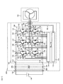
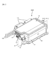
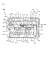
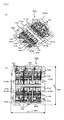
- FIG. 1 shows the control block of a hybrid vehicle. It is a figure explaining the electrical equipment circuit structure of an inverter apparatus. It is a perspective view which shows the external appearance of a power converter device. It is a disassembled perspective view which shows the internal structure of a power converter device. It is the figure which attached the cooling water inlet piping and the outlet piping to the aluminum casting of the housing
- FIG. 7 is a cross-sectional view taken along the line AA in FIG. 6. It is a figure which shows a power module, (a) is an upper perspective view, (b) is a top view. It is a disassembled perspective view of the DC terminal of the power module 300 regarding this embodiment.
- the power module case 302 is a sectional view partially transparent.
- FIG. 3 is a diagram showing a current flow in a power module 300. It is a perspective view which shows the external appearance structure of the capacitor
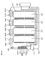
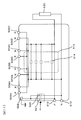
- FIG. 14 is a diagram schematically showing a connection state of the noise filter capacitors 556 and 557 and the discharge resistor 530.
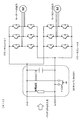
- 6 is a circuit diagram around a capacitor module 500.
- FIG. It is a figure explaining the form by which two power modules were connected with the common capacitor
- FIG. 5 is a diagram showing an electrical flow in an overview diagram of a capacitor module 500. It is a figure showing an electric flow in an outline figure of capacitor module 500 concerning other embodiments. It is the figure which represented the electrical connection inside the capacitor
- FIG. 3 is an external perspective view of a conductive member 570.
- FIG. FIG. 46 is an external view of a conductive member 570. It is an external appearance perspective view of the insulating cover 540 which concerns on this embodiment. It is an external appearance perspective view of the insulating paper 535 which concerns on other embodiment. It is an external appearance perspective view of the insulating cover 545 which concerns on other embodiment.
- FIG. 1 is a diagram showing a control block of a hybrid vehicle.
- the power conversion device is used in a vehicle-mounted power conversion device for a vehicle-mounted electrical system mounted on an automobile, in particular, a vehicle drive electrical system, and has a very severe mounting environment and operational environment.
- the inverter device will be described as an example.
- a vehicle drive inverter device is provided in a vehicle drive electrical system as a control device for controlling the drive of a vehicle drive motor, and a DC power supplied from an onboard battery or an onboard power generator constituting an onboard power source is a predetermined AC power. Then, the AC power obtained is supplied to the vehicle drive motor to control the drive of the vehicle drive motor.
- the vehicle drive inverter device also has a function of converting AC power generated by the vehicle drive motor into DC power according to the operation mode. Yes.
- the converted DC power is supplied to the on-vehicle battery.
- the configuration of the present embodiment is optimal as a power conversion device for driving a vehicle such as an automobile or a truck.
- other power conversion devices such as a power conversion device such as a train, a ship, and an aircraft, and a factory facility are also included.
- a hybrid electric vehicle (hereinafter referred to as “HEV”) 110 is one electric vehicle, and includes two vehicle driving systems.
- One of them is an engine system that uses an engine 120 that is an internal combustion engine as a power source.
- the engine system is mainly used as a drive source for HEV.
- the other is an in-vehicle electric system using motor generators 192 and 194 as a power source.
- the in-vehicle electric system is mainly used as an HEV drive source and an HEV power generation source.
- the motor generators 192 and 194 are, for example, synchronous machines or induction machines, and operate as both a motor and a generator depending on the operation method.
- a front wheel axle 114 is rotatably supported at the front part of the vehicle body.
- a pair of front wheels 112 are provided at both ends of the front wheel axle 114.
- a rear wheel axle (not shown) is rotatably supported on the rear portion of the vehicle body.
- a pair of rear wheels are provided at both ends of the rear wheel axle.
- the HEV of this embodiment employs a so-called front wheel drive system in which the main wheel driven by power is the front wheel 112 and the driven wheel to be driven is the rear wheel. You may adopt.
- a front wheel side differential gear (hereinafter referred to as “front wheel side DEF”) 116 is provided at the center of the front wheel axle 114.
- the front wheel axle 114 is mechanically connected to the output side of the front wheel side DEF 116.
- the output shaft of the transmission 118 is mechanically connected to the input side of the front wheel side DEF 116.
- the front wheel side DEF 116 is a differential power distribution mechanism that distributes the rotational driving force that is shifted and transmitted by the transmission 118 to the left and right front wheel axles 114.
- the output side of the motor generator 192 is mechanically connected to the input side of the transmission 118.
- the output side of the engine 120 and the output side of the motor generator 194 are mechanically connected to the input side of the motor generator 192 via the power distribution mechanism 122.
- Motor generators 192 and 194 and power distribution mechanism 122 are housed inside the casing of transmission 118.
- the motor generators 192 and 194 are synchronous machines having a permanent magnet on the rotor, and the AC power supplied to the armature windings of the stator is controlled by the inverter devices 140 and 142, thereby the motor generators 192 and 194. Is controlled.
- a battery 136 is electrically connected to the inverter devices 140 and 142, and power can be exchanged between the battery 136 and the inverter devices 140 and 142.
- the first motor generator unit composed of the motor generator 192 and the inverter device 140 and the second motor generator unit composed of the motor generator 194 and the inverter device 142 are provided. ing. That is, in the case where the vehicle is driven by the power from the engine 120, when assisting the driving torque of the vehicle, the second motor generator unit is operated as the power generation unit by the power of the engine 120 to generate power. The first electric power generation unit is operated as an electric unit by the obtained electric power. Further, in the same case, when assisting the vehicle speed of the vehicle, the first motor generator unit is operated by the power of the engine 120 as a power generation unit to generate power, and the second motor generator unit is generated by the electric power obtained by the power generation. Operate as an electric unit.
- the vehicle can be driven only by the power of the motor generator 192 by operating the first motor generator unit as an electric unit by the electric power of the battery 136.
- the battery 136 can be charged by generating power by operating the first motor generator unit or the second motor generator unit as the power generation unit by the power of the engine 120 or the power from the wheels.
- the battery 136 is also used as a power source for driving an auxiliary motor 195.
- the auxiliary machine is, for example, a motor that drives a compressor of an air conditioner or a motor that drives a hydraulic pump for control.
- DC power is supplied from the battery 136 to the inverter 43 device, and is converted into AC power by the inverter device 43.
- the inverter device 43 has the same function as the inverter devices 140 and 142, and controls the phase, frequency, and power of alternating current supplied to the motor 195.
- the motor 195 generates torque by supplying AC power having a leading phase with respect to the rotation of the rotor of the motor 195.
- the motor 195 acts as a generator, and the motor 195 is operated in a regenerative braking state.
- Such a control function of the inverter device 43 is the same as the control function of the inverter devices 140 and 142. Since the capacity of the motor 195 is smaller than the capacity of the motor generators 192 and 194, the maximum conversion power of the inverter device 43 is smaller than that of the inverter devices 140 and 142, but the circuit configuration of the inverter device 43 is basically the circuit of the inverter devices 140 and 142. Same as the configuration.
- the inverter devices 140 and 142, the inverter device 43, and the capacitor module 500 are in an electrical close relationship. Furthermore, there is a common point that measures against heat generation are necessary. It is also desired to make the volume of the device as small as possible. From these points, the power conversion device described in detail below includes the inverter devices 140 and 142, the inverter device 43, and the capacitor module 500 in the casing of the power conversion device. With this configuration, a small and highly reliable device can be realized.
- the inverter devices 140 and 142, the inverter device 43, and the capacitor module 500 in one housing, it is effective in simplifying wiring and taking measures against noise.
- the inductance of the connection circuit between the capacitor module 500, the inverter devices 140 and 142, and the inverter device 43 can be reduced, the spike voltage can be reduced, heat generation can be reduced, and heat dissipation efficiency can be improved.
- the electric circuit configuration of the inverter devices 140 and 142 or the inverter device 43 will be described with reference to FIG.
- the case where the inverter devices 140 and 142 or the inverter device 43 are individually configured will be described as an example. Since the inverter devices 140 and 142 or the inverter device 43 have the same functions and the same functions, the inverter device 140 will be described here as a representative example.
- the power conversion device 200 includes an inverter device 140 and a capacitor module 500, and the inverter device 140 includes an inverter circuit 144 and a control unit 170.
- the inverter circuit 144 includes a plurality of upper and lower arm series circuits 150 including an IGBT 328 (insulated gate bipolar transistor) and a diode 156 that operate as an upper arm, and an IGBT 330 and a diode 166 that operate as a lower arm (FIG. 2).
- control unit 170 includes a driver circuit 174 that drives and controls the inverter circuit 144 and a control circuit 172 that supplies a control signal to the driver circuit 174 via the signal line 176.
- the IGBTs 328 and 330 of the upper arm and the lower arm are switching power semiconductor elements, operate in response to a drive signal output from the control unit 170, and convert DC power supplied from the battery 136 into three-phase AC power. .
- the converted electric power is supplied to the armature winding of the motor generator 192.
- the inverter circuit 144 is configured by a three-phase bridge circuit, and a DC positive terminal 314 to which upper and lower arm series circuits 150, 150, 150 for three phases are electrically connected to the positive side and the negative side of the battery 136, respectively. And DC negative electrode terminal 316 are electrically connected in parallel.
- IGBTs 328 and 330 are used as switching power semiconductor elements.
- the IGBTs 328 and 330 include collector electrodes 153 and 163, emitter electrodes (signal emitter electrode terminals 155 and 165), and gate electrodes (gate electrode terminals 154 and 164).
- Diodes 156 and 166 are electrically connected between the collector electrodes 153 and 163 of the IGBTs 328 and 330 and the emitter electrode as shown.
- the diodes 156 and 166 have two electrodes, a cathode electrode and an anode electrode, and the cathode electrode serves as the collector electrode of the IGBTs 328 and 330 so that the direction from the emitter electrode to the collector electrode of the IGBTs 328 and 330 is the forward direction.
- the anode electrodes are electrically connected to the emitter electrodes of the IGBTs 328 and 330, respectively.
- a MOSFET metal oxide semiconductor field effect transistor
- the diode 156 and the diode 166 are not necessary.
- the upper and lower arm series circuit 150 is provided for three phases corresponding to each phase winding of the armature winding of the motor generator 192.
- the three upper and lower arm series circuits 150, 150, 150 are respectively connected to the motor generator 192 via the intermediate electrode 169 and the AC terminal 159 that connect the emitter electrode of the IGBT 328 and the collector electrode 163 of the IGBT 330, the V phase, and the W phase. Is forming.
- the upper and lower arm series circuits are electrically connected in parallel.
- the collector electrode 153 of the upper arm IGBT 328 is connected to the positive capacitor electrode of the capacitor module 500 via the positive terminal (P terminal) 157, and the emitter electrode of the lower arm IGBT 330 is connected to the capacitor module 500 via the negative terminal (N terminal) 158.
- the intermediate electrode 169 corresponding to the middle point portion of each arm is connected to the corresponding phase winding of the armature winding of the motor generator 192 with an AC connector. It is electrically connected via 188.
- the capacitor module 500 is for configuring a smoothing circuit that suppresses fluctuations in DC voltage caused by the switching operation of the IGBTs 328 and 330.
- the positive electrode side of the battery 136 is electrically connected to the positive electrode side capacitor electrode of the capacitor module 500, and the negative electrode side of the battery 136 is electrically connected to the negative electrode side capacitor electrode of the capacitor module 500 via the DC connector 138.
- the capacitor module 500 is connected between the collector electrode 153 of the upper arm IGBT 328 and the positive electrode side of the battery 136, and between the emitter electrode of the lower arm IGBT 330 and the negative electrode side of the battery 136. Electrically connected in parallel to the series circuit 150.
- the control unit 170 is for operating the IGBTs 328 and 330, and generates a timing signal for controlling the switching timing of the IGBTs 328 and 330 based on input information from other control devices or sensors. And a drive circuit 174 that generates a drive signal for switching the IGBTs 328 and 330 based on the timing signal output from the control circuit 172.
- the control circuit 172 includes a microcomputer (hereinafter referred to as “microcomputer”) for performing arithmetic processing on the switching timing of the IGBTs 328 and 330.
- the microcomputer receives as input information the target torque value required for the motor generator 192, the current value supplied from the upper and lower arm series circuit 150 to the armature winding of the motor generator 192, and the magnetic pole of the rotor of the motor generator 192. The position has been entered.
- the target torque value is based on a command signal output from a host controller (not shown).
- the current value is detected based on the detection signal output from the current sensor 180.
- the magnetic pole position is detected based on a detection signal output from a rotating magnetic pole sensor (not shown) provided in the motor generator 192.
- the case where the current values of three phases are detected will be described as an example, but the current values for two phases may be detected.
- the microcomputer in the control circuit 172 calculates the d and q axis current command values of the motor generator 192 based on the target torque value, and the calculated d and q axis current command values and the detected d and q
- the voltage command values for the d and q axes are calculated based on the difference from the current value of the shaft, and the calculated voltage command values for the d and q axes are calculated based on the detected magnetic pole position. Convert to W phase voltage command value.
- the microcomputer generates a pulse-like modulated wave based on the comparison between the fundamental wave (sine wave) and the carrier wave (triangular wave) based on the voltage command values of the U-phase, V-phase, and W-phase, and the generated modulation
- the wave is output to the driver circuit 174 as a PWM (pulse width modulation) signal.
- the driver circuit 174 When driving the lower arm, the driver circuit 174 amplifies the PWM signal, and when the driver circuit 174 drives the upper arm to the gate electrode of the corresponding IGBT 330 of the lower arm, the driver circuit 174 sets the level of the reference potential of the PWM signal. After shifting to the level of the reference potential of the upper arm, the PWM signal is amplified and output as a drive signal to the gate electrode of the corresponding IGBT 328 of the upper arm. As a result, each IGBT 328, 330 performs a switching operation based on the input drive signal.
- control unit 170 performs abnormality detection (overcurrent, overvoltage, overtemperature, etc.) to protect the upper and lower arm series circuit 150. For this reason, sensing information is input to the control unit 170. For example, information on the current flowing through the emitter electrodes of the IGBTs 328 and 330 is input to the corresponding drive units (ICs) from the signal emitter electrode terminals 155 and 165 of each arm. Thereby, each drive part (IC) detects overcurrent, and when overcurrent is detected, the switching operation of corresponding IGBT328,330 is stopped, and corresponding IGBT328,330 is protected from overcurrent.
- ICs drive unit
- Information on the temperature of the upper and lower arm series circuit 150 is input to the microcomputer from a temperature sensor (not shown) provided in the upper and lower arm series circuit 150.
- voltage information on the DC positive side of the upper and lower arm series circuit 150 is input to the microcomputer.
- the microcomputer performs over-temperature detection and over-voltage detection based on the information, and when an over-temperature or over-voltage is detected, it stops the switching operation of all the IGBTs 328 and 330, and the upper and lower arm series circuit 150 (subtract)
- the semiconductor module including the circuit 150 is protected from overtemperature or overvoltage.
- the upper and lower arm series circuit 150 includes a positive terminal (P terminal, positive terminal) 157, a negative terminal (N terminal 158, negative terminal), an AC terminal 159 from the intermediate electrode 169 of the upper and lower arms, and an upper arm signal.
- the power conversion device 200 has a DC connector 138 on the input side and an AC connector 188 on the output side, and is connected to the battery 136 and the motor generator 192 through the connectors 138 and 188, respectively. Further, as a circuit for generating an output of each phase of the three-phase alternating current to be output to the motor generator, a power conversion device having a circuit configuration in which two upper and lower arm series circuits are connected in parallel to each phase may be used.
- 200 is a power converter
- 10 is an upper case
- 11 is a metal base plate
- 12 is a housing
- 13 is a cooling water inlet pipe
- 14 is a cooling water outlet pipe
- 420 is a cover
- 16 is a lower part.
- the case, 17 is an AC terminal case
- 18 is an AC terminal
- 19 is a cooling water flow path
- 20 is a control circuit board that holds the control circuit 172.
- Reference numeral 21 denotes a connector for connection to the outside
- reference numeral 22 denotes a drive circuit board that holds a driver circuit 174.
- Two power modules (semiconductor module units) 300 are provided, and an inverter circuit 144 is built in each power module.
- 700 is a flat laminated bus bar
- 800 is an O-ring
- 304 is a metal base
- 188 is an AC connector
- 314 is a DC positive terminal
- 316 is a DC negative terminal
- 500 is a capacitor module
- 502 is a capacitor case
- 504 is a positive capacitor terminal
- Reference numeral 506 denotes a negative side capacitor terminal
- 514 denotes a capacitor cell.
- FIG. 3 is an external perspective view of the overall configuration of the power conversion device according to the embodiment of the present invention.
- the external appearance of the power conversion device 200 according to the present embodiment is as follows.
- the casing 12 whose top surface or bottom surface is substantially rectangular, the cooling water inlet pipe 13 provided on one of the outer circumferences on the short side of the casing 12, and the cooling water.
- the outlet pipe 14, the upper case 10 for closing the upper opening of the housing 12, and the lower case 16 for closing the lower opening of the housing 12 are fixedly formed. Since the shape of the bottom view or the top view of the housing 12 is substantially rectangular, it is easy to attach to the vehicle and to produce easily.
- AC terminal 18 electrically connects power module 300 and motor generators 192 and 194, and transmits an AC current output from power module 300 to motor generators 192 and 194.
- the connector 21 is connected to the control circuit board 20 built in the housing 12 and transmits various signals from the outside to the control circuit board 20.
- the DC power supply side negative electrode side connection terminal portion 510 and the DC power supply side positive electrode side connection terminal portion 512 electrically connect the battery 136 and the capacitor module 500.
- the connector 21 is provided on one side of the outer peripheral surface on the short side of the housing 12.
- the negative electrode side connecting terminal portion 510 on the DC power source side and the positive electrode side connecting terminal portion 512 on the DC power source side are provided on the outer peripheral surface on the short side opposite to the surface on which the connector 21 is provided. That is, the connector 21 and the negative electrode side connection terminal portion 510 on the DC power supply side are arranged apart from each other. As a result, noise that enters the housing 12 from the negative electrode side connection terminal portion 510 on the DC power supply side and propagates to the connector 21 can be reduced, and the controllability of the motor by the control circuit board 20 can be improved.
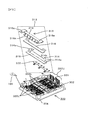
- FIG. 4 is a perspective view in which the entire configuration of the power conversion device according to the embodiment of the present invention is disassembled into components.
- a cooling water channel 19 is provided in the middle of the casing 12, and two sets of openings 400 and 402 are formed in the upper part of the cooling water channel 19 side by side in the flow direction.
- Two power modules 300 are fixed to the upper surface of the cooling water channel 19 so that the two sets of openings 400 and 402 are respectively closed by the power module 300.
- Each power module 300 is provided with fins 305 for radiating heat, and the fins 305 of each power module 300 protrude into the cooling water flow from the openings 400 and 402 of the cooling water channel 19, respectively.
- An opening 404 for facilitating aluminum casting is formed below the cooling water channel 19, and the opening 404 is closed with a cover 420.
- An auxiliary inverter device 43 is attached to the lower side of the cooling water passage 19.
- the auxiliary inverter 43 has a built-in circuit similar to the inverter circuit 144 shown in FIG. 2, and has a power module with a built-in power semiconductor element constituting the inverter circuit 144.
- the auxiliary inverter device 43 is fixed to the lower surface of the cooling water passage 19 so that the heat dissipation metal surface of the built-in power module faces the lower surface of the cooling water passage 19.
- an O-ring 800 for sealing is provided between the power module 300 and the housing 12, and an O-ring 802 is also provided between the cover 420 and the housing 12.
- the sealing material is an O-ring, but a resin material, a liquid seal, a packing, or the like may be used instead of the O-ring.
- the power converter 200 can be easily assembled. Can be improved.
- a lower case 16 is provided in the lower part of the cooling water flow path 19 so as to dissipate heat.
- the capacitor case 500 is disposed in the lower case 16, and the heat dissipation surface of the case made of a metal material of the capacitor module 500 It is fixed to the surface of the lower case 16 so as to face the surface.
- the casing 12 provided with the cooling water flow path 19 is cooled, whereby the lower case 16 provided at the lower portion of the casing 12 is cooled, and by this cooling, the heat of the capacitor module 500 is transferred to the lower case 16 and the casing.
- the capacitor module 500 is cooled by being thermally conducted to the cooling water through the body 12.
- a laminated conductor plate 700 for electrically connecting the power module 300 and the capacitor module 500 is disposed above the power module 300.
- the laminated conductor plate 700 is configured to be wide in the width direction of the two power modules 300 across the two power modules 300.
- the laminated conductor plate 700 includes a positive electrode side conductor plate 702 connected to the positive electrode side terminal of the capacitor module 500, a negative electrode side conductor plate 704 connected to the negative electrode side terminal, the positive electrode side terminal and the negative electrode side terminal. It is comprised by the insulation member arrange
- the laminated conductor plate 700, the power module 300, and the capacitor module 500 can be electrically connected. Even if it is a power converter provided, the assembly man-hour can be suppressed.
- a control circuit board 20 and a drive circuit board 22 are disposed above the laminated conductor plate 700.
- the driver circuit 174 shown in FIG. 2 is mounted on the drive circuit board 22, and the CPU shown in FIG.
- a control circuit 172 having is mounted.
- a metal base plate 11 is disposed between the drive circuit board 22 and the control circuit board 20, and the metal base plate 11 functions as an electromagnetic shield for a circuit group mounted on both the boards 22 and 20, and also the drive circuit board.
- the heat generated by the control circuit board 20 and the control circuit board 20 is released and cooled.
- the cooling water flow path 19 is provided in the central portion of the housing 19, the power module 300 for driving the vehicle is arranged on one side thereof, and the power module 43 for auxiliary machines is arranged on the other side.
- cooling can be efficiently performed in a small space, and the entire power conversion device can be downsized. Further, by making the main structure of the cooling water channel 19 at the center of the casing by casting an aluminum material integrally with the casing 12, the cooling water channel 19 has the effect of increasing the mechanical strength in addition to the cooling effect. Further, by making the aluminum casting, the housing 12 and the cooling water flow path 19 are integrated with each other, heat conduction is improved, and cooling efficiency is improved.
- the drive circuit board 22 is provided with an inter-board connector 23 that passes through the metal base plate 11 and is connected to a circuit group of the control circuit board 20.
- the control circuit board 20 is provided with a connector 21 for electrical connection with the outside.
- the connector 21 transmits a signal to, for example, a lithium battery module mounted on the vehicle as the battery 136, for example, outside the power conversion device, and a signal indicating the state of the battery from the lithium battery module or a charging state of the lithium battery. A signal is sent.
- the inter-board connector 23 is provided in order to exchange signals with the control circuit 172 held on the control circuit board 20, and the signal line 176 shown in FIG.
- the signal of the switching timing of the inverter circuit is transmitted from the control circuit board 20 to the drive circuit board 22 via the signal line 176 and the board-to-board connector 23, and the drive circuit board 22 generates a gate drive signal as a drive signal. Each is applied to the gate electrode of the power module.
- Openings are formed in the upper and lower portions of the housing 12, and these openings are closed by fixing the upper case 10 and the lower case 16 to the housing 12 with screws or the like, respectively.
- a cooling water channel 19 is provided in the center of the housing 12, and the power module 300 and the cover 420 are fixed to the cooling water channel 19. In this way, the cooling water channel 19 is completed, and a water leak test of the water channel is performed. When the water leakage test is passed, the operation of attaching the substrate and the capacitor module 500 from the upper and lower openings of the housing 12 can be performed next. In this way, the cooling water flow path 19 is arranged in the center, and then the structure for performing the work of fixing the necessary parts from the upper and lower openings of the housing 12 is made, and the productivity is improved. Moreover, it becomes possible to complete the cooling water flow path 19 first and to attach other parts after the water leak test, which improves both productivity and reliability.
- FIG. 5 is a view in which a cooling water inlet pipe and an outlet pipe are attached to an aluminum casting product of the casing 12 having the cooling water flow path 19,
- FIG. 5A is a perspective view of the casing 12
- FIG. FIG. 5C is a top view of the housing 12,
- FIG. 5C is a bottom view of the housing 12.
- the casing 12 and a cooling water flow path 19 provided in the casing 12 are integrally cast.
- the upper surface or the lower surface of the housing 12 has a substantially rectangular shape, and a cooling water inlet pipe 13 for taking in cooling water is provided on the side surface of one side of the rectangular short side, and the cooling water inlet pipe 14 is provided on the same side surface. Is provided.
- the cooling water flowing into the cooling water flow path 19 from the cooling water inlet pipe 13 flows along the long side of the rectangle in the direction of the arrow 418, and the arrows 421a and 421b near the front side of the other side of the short side of the rectangle. And flows again in the direction of the arrow 422 along the long side of the rectangle, and flows out from an outlet hole (not shown).
- Two openings 400 and 402 are respectively formed on the outgoing side and the return side of the cooling water passage 19.
- the power modules 300 are fixed to the openings, respectively, and fins for heat dissipation of the power modules 300 protrude from the openings into the flow of cooling water.
- the power modules 300 are aligned and fixed in the flow direction of the casing 12, that is, along the long side, and by this fixing, the opening of the cooling water flow path 19 is completely blocked by, for example, the O-ring 800 or the like.
- the support portion 410 is formed integrally with the housing so that the The support portion 410 is located at substantially the center of the housing 12, and one power module 300 is fixed toward the inlet / outlet side of the cooling water with respect to the support portion 410, and the cooling water is connected to the support portion 410.
- One other power module 300 is fixed toward the folded side.
- a screw hole 412 shown in FIG. 5B is used to fix the power module 300 on the entrance / exit side to the cooling water flow path 19, and the opening 400 is sealed by this fixing.
- the screw hole 414 is used to fix the power module 300 on the folding side to the cooling water channel 19, and the opening 402 is sealed by this fixing.
- the power module 300 on the inlet / outlet side is cooled by the cold cooling water from the cooling water inlet pipe 13 and the cooling water warmed by the heat from the heat generating component near the outlet side.
- the folded-back power module 300 is cooled by the slightly warmed cooling water and the cooling water that is slightly cooler than the cooling water near the outlet hole 403.
- the arrangement relationship between the folded cooling passage and the two power modules 300 has an advantage that the cooling efficiency of the two power modules 300 is balanced.
- the support portion 410 is used for fixing the power module 300 and is necessary for sealing the openings 400 and 402. Further, the support portion 410 has a great effect on strengthening the strength of the housing 12.
- the cooling water channel 19 has a folded shape as described above, and is provided with a partition 408 that separates the going-side channel and the returning-side channel, and the partition 408 is formed integrally with the support portion 410.
- the partition wall 408 not only simply separates the going-side flow path and the return-side flow path but also acts to increase the mechanical strength of the housing. Also, it acts as a heat transfer passage between the turn-back passages and makes the temperature of the cooling water uniform. If the temperature difference between the inlet side and the outlet side of the cooling water is large, uneven cooling efficiency increases. Although the temperature difference to some extent is unavoidable, the partition wall 408 is formed integrally with the support portion 410, so that there is an effect of suppressing the temperature difference of the cooling water.
- FIG. 5C shows the back surface of the cooling water channel 19, and an opening 404 is formed on the back surface corresponding to the support portion 410.
- the opening 404 is for improving the yield of the support portion 410 and the housing 12 integrated structure formed by casting the housing.
- the formation of the opening 404 eliminates the double structure of the support portion 410 and the bottom portion of the cooling water channel 19 in the cast product, facilitating casting, and improving productivity.
- a through hole 406 is formed in the side portion of the cooling water passage 19. Electrical components (power module 300 and capacitor module 500) installed on both sides of the cooling water channel 19 are connected through the through hole 406.
- the casing 12 can be manufactured as an integral structure of the cooling water flow path 19 and the casing 12, it is suitable for casting production, particularly aluminum die casting production.
- FIG. 6 shows a state where the power module 300 is fixed to the upper surface opening of the cooling water passage 19 and the cover 420 is further fixed to the rear surface opening.
- an AC power line 186 and an AC connector 188 protrude from the housing 12.
- the through hole 406 is formed inside the other long side of the rectangle of the housing 12, and a part of the laminated conductor plate 700 connected to the power module 300 through the through hole 406 can be seen.
- the auxiliary inverter device 43 is disposed in the vicinity of the side surface of the housing 12 to which the DC positive electrode side connection terminal portion 512 is connected. Further, a capacitor module 500 is disposed below the auxiliary inverter device 43 (on the side opposite to the side where the cooling water flow path 19 is present).
- the auxiliary machine positive terminal 44 and the auxiliary machine negative terminal 45 protrude downward (in the direction in which the capacitor module 500 is disposed), and are connected to the auxiliary machine positive terminal 532 and the auxiliary machine negative terminal 534 on the capacitor module 500 side, respectively.
- the auxiliary inverter device 43 is disposed in the gap between the cooling water flow path 19 and the capacitor module 500, and the auxiliary inverter device 43 has the same height as the cover 420. Therefore, the auxiliary inverter device 43 can be cooled and an increase in the height of the power conversion device 200 can be suppressed.
- the cooling water inlet pipe 13 and the cooling water outlet pipe 14 are fixed by screws.
- the water leakage inspection of the cooling water channel 19 can be performed.
- the auxiliary inverter device 43 is attached to the one that has passed this inspection, and the capacitor module 500 is further attached.
- FIG. 7 is a cross-sectional view of the power conversion device 200 (AA cross-section reference of FIG. 6), and the basic structure is as already described based on FIGS.
- a cooling water passage 19 (dotted line portion in FIG. 7) made of aluminum die casting is provided integrally with the housing 12 at the center in the vertical direction in the cross section of the housing 12, and is formed on the upper surface side of the cooling water passage 19.
- the power module 300 (the chain line portion in FIG. 7) is installed in the opened opening.
- the left side with respect to the paper surface of FIG. 7 is the outgoing path 19a on the cooling water direction
- the right side with respect to the paper surface is the return path 19b on the return side of the water channel.
- the forward path 19a and the return path 19b are each provided with an opening, and the opening is blocked by the metal base 304 for heat dissipation of the power module 300 so as to straddle both the forward path 19a and the return path 19b.
- Fins 305 for heat dissipation provided in 304 protrude from the opening in the flow of cooling water.
- an auxiliary inverter device 43 is fixed to the lower surface side of the cooling water passage 19.
- a plate-like AC power line 186 having a substantially bent center is connected to the AC terminal 159 of the power module 300 at one end and protrudes from the power converter 200 to form an AC connector.
- the positive electrode side capacitor terminal 504 and the negative electrode side capacitor terminal 506 are electrically and mechanically connected to the positive electrode side conductor plate 702 and the negative electrode side conductor plate 704 through the through holes 406 (two-dot chain line portion in FIG. 7), respectively.
- the A cooling water flow path 19 that reciprocates substantially in the center of the housing 12 in the long side direction of the rectangle is disposed, and an AC connector 188, a positive-side capacitor terminal 504, and a negative-side capacitor terminal are arranged in a direction substantially perpendicular to the cooling water flow direction. 506 is arranged.
- the electrical wiring is arranged in an orderly manner, which leads to a reduction in size of the power conversion device 200. Since the positive electrode side conductor plate 702 and the negative electrode side conductor plate 704 of the laminated conductor plate 700 and the AC side power line 186 project outside the power module 300 to form connection terminals, the structure is very simple, and other connection conductors are provided. Because it is not used, it is downsized. This structure improves productivity and improves reliability.
- the through hole 406 is separated from the cooling water flow path 19 by a frame inside the housing 12, and the positive electrode side conductor plate 702 and the negative electrode side conductor plate 704, the positive electrode side capacitor terminal 506, and the negative electrode side capacitor terminal 504. Therefore, the reliability is improved.
- the power module 300 having a large calorific value is fixed to one surface of the cooling water channel 19 and the fins 305 of the power module 300 protrude from the opening of the cooling water channel 19 into the water channel for efficient cooling.
- the auxiliary inverter device 43 having a large amount of heat is cooled on the other surface of the cooling water flow path 19, and the capacitor module 500 having the next largest heat generation amount is cooled via the housing 12 and the lower case 16.
- the capacitor module 500 can be used as a smoothing capacitor of the auxiliary inverter device 43.
- the wiring distance is shortened. There is.
- the wiring distance is short, the inductance can be reduced.
- a drive circuit board 22 on which a driver circuit 174 is mounted is disposed above the power module 300, and a control circuit board is interposed above the drive circuit board 22 with a metal base plate 11 that enhances the effects of heat dissipation and electromagnetic shielding. 20 is arranged.
- the control circuit board 20 is mounted with the control circuit 172 shown in FIG. By fixing the upper case 10 to the housing 12, the power conversion device 200 according to the present embodiment is configured.
- the drive circuit board 22 is arranged between the control circuit board 20 and the power module 300, the operation timing of the inverter circuit is transmitted from the control circuit board 20 to the drive circuit board 22, and based on that.
- a gate signal is generated by the drive circuit board 22 and applied to each gate of the power module 300. Since the control circuit board 20 and the drive circuit board 22 are thus arranged along the electrical connection relationship, the electrical wiring can be simplified and the power converter 200 can be downsized.
- the drive circuit board 22 is disposed at a distance closer to the control circuit board 20 than the power module 300 and the capacitor module 500. Therefore, the wiring distance from the drive circuit board 22 to the drive circuit board 20 is shorter than the wiring distance between other components (such as the power module 300) and the control circuit board 20. Therefore, electromagnetic noise transmitted from the DC positive electrode side connection terminal portion 512 and electromagnetic noise due to the switching operation of the IGBTs 328 and 330 can be prevented from entering the wiring from the drive circuit board 22 to the drive circuit board 20.
- the power module 300 is fixed to one surface of the cooling water channel 19 and the auxiliary inverter device 43 is fixed to the other surface, so that the power module 300 and the auxiliary inverter device 43 are simultaneously cooled by the cooling water channel 19. To do.
- the power module 300 has a greater cooling effect because the fins for heat dissipation are in direct contact with the cooling water in the cooling water passage 19.
- the casing 12 is cooled by the cooling water flow path 19, and the lower case 16 and the metal base plate 11 are fixed to the casing 12, thereby cooling through the lower case 16 and the metal base plate 11. Since the metal case of the capacitor module 500 is fixed to the lower case 16, the capacitor module 500 is cooled via the lower case 16 and the housing 12.
- the control circuit board 20 and the drive circuit board 22 are cooled via the metal base plate 11.
- the lower case 16 is also made of a material having good thermal conductivity, receives heat generated from the capacitor module 500, conducts heat to the housing 19, and is radiated by the cooling water in the cooling water passage 19.
- an inverter device 43 for auxiliary equipment having a relatively small capacity which is used for an air conditioner for a vehicle, an oil pump, and a pump for other purposes, is installed. The heat generated from the auxiliary inverter device 43 is radiated by the cooling water in the cooling water passage 19 through the intermediate frame of the housing 12.
- the cooling water flow path 19 is provided in the center, the metal base plate 11 is provided on one side, and the lower case 16 is provided on the other side. It can cool well. Also, the components are neatly arranged inside the power conversion device 200, and the size can be reduced.
- the heat radiator that performs the heat dissipation function of the power conversion device is primarily the cooling water flow path 19, but the metal base plate 11 also performs this function (the metal base plate 11 is used to perform the heat dissipation function). Provided).
- the metal base plate 11 performs an electromagnetic shielding function, receives heat from the control circuit board 20 and the drive circuit board 22, conducts heat to the housing 12, and is radiated by the cooling water in the cooling water flow path 19.
- the power converter according to the present embodiment has a multilayer structure in which the radiator is a three-layered structure, that is, the metal base plate 11, the cooling water channel 19, and the lower case 16, and these
- the heat radiators are hierarchically installed adjacent to the respective heat generators (power module 300, control circuit board 20, drive circuit board 22, and capacitor module 500).
- the cooling water flow path 19 In the center of the hierarchical structure, there is a cooling water flow path 19 that is a main radiator, and the metal base plate 11 and the lower case 16 are structured to transmit heat to the cooling water in the cooling water flow path 19 through the housing 12.
- Three heat radiators (cooling water flow path 19, metal base plate 11, lower case 16) are accommodated in the housing 12 to improve heat dissipation and contribute to reduction in thickness and size.
- the capacitor element 514 is configured such that the side surface of the columnar element is crushed from both ends and the cross section thereof is elliptical in order to improve the integration efficiency.
- the cylindrical side surface forming the major axis side in the elliptical cross section is disposed to face the bottom of the capacitor case 502. Thereby, the contact area between the capacitor element 514 and the capacitor case 502 increases, the capacitor element 514 can be efficiently cooled, and the height of the power conversion device 200 can be reduced.
- the heat generated by the capacitor element 514 can be radiated to the outside via the capacitor case 502 and the lower case 16.
- the arrangement of the element 514 is particularly effective for improving heat dissipation.
- FIG. 8A is a top perspective view of the power module 300 according to the present embodiment
- FIG. 8B is a top view of the power module 300.
- FIG. 9 is an exploded perspective view of a DC terminal of the power module 300 according to the present embodiment.
- FIG. 10 is a cross-sectional view in which the power module case 302 is partially transparent in order to make the structure of the DC bus bar easier to understand.
- FIG. 9A is a diagram in which one of the metal base 304 and three upper and lower arm series circuits, which are components of the power module 300, is extracted.
- FIG. 9B is an exploded perspective view of the metal base 304, the circuit wiring pattern, and the insulating substrate 334.
- 302 is a power module case
- 304 is a metal base
- 305 is a fin
- 314 is a DC positive terminal
- 316 is a DC negative terminal
- 318 is insulating paper (see FIG. 9)
- 320U / 320L is a power module control Terminals
- 328 are upper arm IGBTs
- 330 are lower arm IGBTs
- 156/166 are diodes
- 334 is an insulating substrate (see FIG. 10)
- 334k is a circuit wiring pattern on the insulating substrate 334 (see FIG. 10)
- Reference numeral 334r denotes a circuit wiring pattern 337 (see FIG. 10) under the insulating substrate 334.
- the power module 300 is roughly divided into, for example, a semiconductor module portion including wiring in a power module case 302 made of a resin material, a metal base 304 made of a metal material such as Cu, Al, AlSiC, and a connection terminal ( DC positive terminal 314, control terminal 320U, etc.).
- the power module 300 has U, V, and W phase AC terminals 159 for connecting to the motor, and a DC positive terminal 314 and a DC negative terminal 316 that are connected to the capacitor module 500. ing.
- the semiconductor module part is provided with IGBTs 328 and 330 of upper and lower arms, a diode 156/166, etc. on an insulating substrate 334, and is protected by a resin or silicon gel (not shown).
- the insulating substrate 334 may be a ceramic substrate or a thinner insulating sheet.
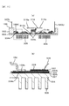
- FIG. 8B shows an arrangement configuration in which the upper and lower arm series circuits are specifically arranged on the insulating substrate 334 made of ceramic having good thermal conductivity fixed to the metal base 304. It is explanatory drawing which shows a figure and its function.
- the IGBTs 328 and 330 and the diodes 327 and 332 shown in FIG. 8B respectively connect two chips in parallel to form an upper arm and a lower arm, and increase the current capacity that can be supplied to the upper and lower arms.
- the DC terminal 313 built in the power module 300 has a laminated structure of a DC negative terminal 316 and a DC positive terminal 314 with an insulating paper 318 interposed therebetween (dotted line portion in FIG. 9). Further, the ends of the DC negative electrode terminal 316 and the DC positive electrode terminal 314 are bent in opposite directions to form a negative electrode connecting portion 316a and a positive electrode connecting portion 314a for electrically connecting the laminated conductor plate 700 and the power module 300. To do. By providing two connection portions 314a (or 316a) with the laminated conductor plate 700, the average distances from the negative electrode connection portion 316a and the positive electrode connection portion 314a to the three upper and lower arm series circuits are substantially equal. Variations in parasitic inductance in 300 can be reduced.
- the negative electrode connection portion 316a and the positive electrode connection portion 314a are bent in opposite directions.
- the insulating paper 318 is bent along the negative electrode connecting portion 316a to ensure an insulating creepage distance between the positive and negative terminals.
- the insulating paper 318 when heat resistance is required, a sheet in which polyimide, meta-aramid fiber, polyester with improved tracking properties, or the like is used is used. In addition, in consideration of defects such as pin fall, two sheets are stacked to increase reliability.
- the corners are rounded or the sag surface at the time of punching faces the insulating paper so that the edge of the terminal does not touch the insulating paper.
- insulating paper is used as the insulator, but as another example, the terminal may be coated with the insulator.
- the distance between the positive electrode and the negative electrode is 0.5 mm or less, and the thickness of the insulating paper is half or less.
- the DC positive terminal 314 and the DC negative terminal 316 have connection ends 314K and 316K for connecting to the circuit wiring pattern 334K.
- Each connection end 314K, 316K protrudes in the direction of the circuit wiring pattern 334K, and its tip is bent to form a joint surface with the circuit wiring pattern 334K.
- the connection ends 314K, 316K and the circuit wiring pattern 334K are connected via solder or the like, or directly connected to each other by ultrasonic welding.
- the power module 300 expands and contracts due to the temperature cycle. Due to the expansion and contraction, the connection portion between the connection ends 314K and 316K and the circuit wiring pattern 334K may be cracked or broken. Therefore, in the power module 300 according to the present embodiment, as shown in FIG. 9, the laminated flat surface portion 319 formed by laminating the DC positive terminal 314 and the DC negative terminal 316 is provided on the side where the insulating substrate 334 is mounted. Thus, the laminated flat surface portion 319 can be warped in response to the warping of the metal base 304 caused by the expansion and contraction described above. It becomes.
- connection ends 314 ⁇ / b> K and 316 ⁇ / b> K formed integrally with the laminated flat surface portion 319 can be reduced with respect to the warp of the metal base 304. Therefore, the stress applied in the vertical direction of the joint surface between the connection ends 314K and 316K and the circuit wiring pattern 334K can be relaxed, and cracks or breakage of the joint surface can be prevented.
- the lamination plane part 319 has the width direction length of the lamination plane part 319 so that the metal base 304 can bend in response to both the width direction and the depth direction curvature.
- the length in the depth direction is increased to 130 mm and the length in the depth direction to 10 mm.
- the thickness of each of the stacked flat surface portions 319 of the DC positive electrode terminal 314 and the DC negative electrode terminal 316 is set to be relatively thin as 1 mm so as to facilitate the warping operation.
- the metal base 304 has a fin shape 305 on the opposite side of the insulating substrate 334 in order to efficiently radiate heat to the cooling water by being immersed in the cooling water flow path.
- the metal base 304 is mounted with an IGBT or a diode constituting an inverter circuit on one surface, and a resin power module case 302 is provided on the outer periphery of the metal base 304.
- the fin 305 is brazed to the other surface of the metal base 304 or the metal base 304 and the fin 305 are integrally formed by forging.
- the metal base 304 and the fin 305 are integrally formed by forging, so that the productivity of the power module 300 is improved, the thermal conductivity from the metal base 304 to the fin 305 is improved, and the heat dissipation of the IGBT and the diode is improved. Can be made. Further, by setting the Vickers hardness of the metal base 304 to 60 or more, the ratchet deformation of the metal base 304 caused by the temperature cycle can be suppressed, and the sealing performance between the metal base 304 and the housing 12 can be improved. Further, as shown in FIG. 10A, fins 305 are provided corresponding to the upper and lower arms, respectively, and these fins 305 project into the water channel from the opening of the reciprocating cooling water channel 19. A metal surface around the fin 305 of the metal base 304 is used to close an opening provided in the cooling water channel 19.
- the fin 305 shape of this embodiment is a pin type
- the straight type formed along the flow direction of the cooling water may be used.
- the straight type is used for the fin 305 shape, the pressure for flowing the cooling water can be reduced, and when the pin type is used, the cooling efficiency can be improved.
- An insulating substrate 334 is fixed to one surface of the metal base 304, and an upper arm IGBT 328, an upper arm diode 156, a lower arm IGBT 330, and a lower arm are fixed to the insulating substrate 334 with solder 337.
- the chip of the diode 166 is fixed.
- the upper and lower arm series circuit 150 includes an upper arm circuit 151 and a lower arm circuit 152, a terminal 370 for connecting the upper and lower arm circuits 151 and 152, and an AC power for output.
- An AC terminal 159 is provided.
- the upper arm circuit 151 includes an insulating substrate 334 on which a circuit wiring pattern is formed on a metal base 304, and further an IGBT 328 and a diode 156 on the circuit wiring pattern 334k. Prepare.
- the electrode on the back surface side and the circuit wiring pattern 334k are joined by solder.
- the insulating substrate 334 on which the circuit wiring pattern is formed has a so-called solid pattern having no pattern on the surface (back surface) opposite to the circuit wiring pattern surface.
- the solid pattern on the back surface of the insulating substrate and the metal base 304 are joined by solder.
- the lower arm circuit 152 is mounted on the insulating substrate 334 disposed on the metal base 304, the circuit wiring pattern 334k wired on the insulating substrate 334, and the circuit wiring pattern 334k.
- the IGBT 330 and the diode 166 are provided.
- each arm of each phase in the present embodiment is configured by connecting two sets of the circuit units in parallel with one set of the circuit unit in which the IGBT 328 and the diode 156 are connected in parallel. How many sets of these circuits are connected in parallel is determined by the amount of current supplied to the motor 192. If a larger current than the current supplied to the motor 192 according to the present embodiment is required, the circuit portion is Three or more sets are connected in parallel. On the other hand, when the motor can be driven with a small current, each arm of each phase is configured by only one set of circuit units.
- connection conductor portion 371D flows through the connection portions 374U and 374D of the terminal 370.
- the upper arm is configured by connecting two sets of circuit units in which IGBT 328 and diode 156 are connected in parallel, in parallel. Therefore, in the current path of (2), the current is branched into two at the element side connection conductor portion 372U, and the branched current flows to the two sets of circuit portions.
- connection conductor portion 373D flows through the wire 336
- DC negative electrode terminal 316 (not shown) flows from the connection conductor portion 373D.
- the lower arm is configured by connecting two sets of circuit units in which the IGBT 330 and the diode 166 are connected in parallel in the same manner as the upper arm, in the current path of (1) above, the current is supplied to the element side connecting conductor unit. It is branched into two at 371D, and the branched current flows to two sets of circuit units.
- the connecting conductor portion 371U for connecting the IGBT 328 (and the diode 156) of the upper arm circuit and the DC positive electrode terminal 314 (not shown) is disposed in the vicinity of the substantially central portion of one side of the insulating substrate 334.
- the IGBT 328 (and the diode 156) is mounted in the vicinity of the other side that is opposite to the one side of the insulating substrate 334 on which the connection conductor portion 371U is disposed.
- the two connecting conductor portions 373U are arranged in a row on the one side of the insulating substrate 334 with the connecting conductor portion 371U interposed therebetween.
- Such a circuit pattern and a mounting pattern that is, a circuit wiring pattern on the insulating substrate 334, includes two wiring patterns (371U) on both sides of a generally T-shaped wiring pattern and a generally T-shaped vertical bar (371U).
- the transient current path at the time of switching of the IGBT 328 is an M-shaped current path as indicated by an arrow 350 (broken line) in FIG. It becomes two small loop current paths (the direction of the arrow is when the lower arm is turned on).
- a magnetic field 350H in the direction of the arrow 350H (solid line) in FIG. 11B is generated around these two small loop current paths.
- the magnetic field 350H induces an induced current, so-called eddy current 340, in the metal base 304 disposed below the insulating substrate 334.
- the eddy current 340 generates a magnetic field 340H in a direction that cancels the magnetic field 350H, and can reduce the parasitic inductance generated in the upper arm circuit.
- the two small loop currents described above can generate two U-turn currents such that the currents flowing on the insulating substrate 334 cancel each other. For this reason, as shown in the magnetic field 350H of FIG. 9B, a smaller loop magnetic field is generated inside the power module 300, and therefore, the parasitic inductance can be reduced. Furthermore, since the magnetic field loop generated at the time of switching is small and the magnetic field loop can be confined inside the power module, the induced current to the housing outside the power module is reduced, and the malfunction of the control board or the outside of the power converter Electromagnetic noise can be prevented.
- the lower arm circuit side also has the same circuit wiring pattern and mounting pattern as the above upper arm. That is, the connection conductor portion 371D for connecting the IGBT 330 (and the diode 166) of the lower arm circuit and the DC negative electrode terminal 316 (not shown) is disposed in the vicinity of the substantially central portion of one side of the insulating substrate 334.
- the IGBT 330 (and the diode 166) is mounted in the vicinity of the other side opposite to the one side of the insulating substrate 334 on which the connection conductor portion 371D is disposed.
- the two connecting conductor portions 373D are arranged in a row on the one side of the insulating substrate 334 with the connecting conductor portion 371D interposed therebetween.
- the above-described parasitic inductance can be reduced also on the lower arm circuit side.
- the entrance of the current path of each arm of each phase is, for example, the connection conductor part 371U sandwiched between the two connection conductor parts 373U, while the exit of the current path is the two connection conductor parts 373U. It has become.
- the aforementioned small loop current path is formed in each arm of each phase. Therefore, as described above, it is possible to reduce the parasitic inductance of each arm of each phase and prevent electromagnetic noise.
- FIG. 12 is a perspective view showing an external configuration of the capacitor module 500 according to the present embodiment.
- FIG. 13 is a perspective view showing a state before a filler (sealing material) 522 such as a resin is filled so that the inside of the capacitor module 500 shown in FIG. 12 can be seen.
- a filler (sealing material) 522 such as a resin
- 500 is a capacitor module
- 502 is a capacitor case
- 504 is a negative side capacitor terminal
- 506 is a positive side capacitor terminal
- 510 is a DC negative side connection terminal part
- 512 is a DC positive side connection terminal part
- 514 Represents a capacitor element.
- the capacitor module 500 is disposed at the lower part of the housing 12 and mounted on the upper part of the lower case 16.
- the capacitor case 502 is fixed to the lower case 16 at the four corners by bolts 559A to 559D.
- the capacitor case 502 and the lower case 16 are in contact with each other via a heat dissipating grease (not shown).
- a heat dissipating grease not shown.
- the heat generated by the capacitor element 514 can be released to the metal lower case 16 via the capacitor case 502 and the heat dissipating grease.
- the vibration of the vehicle can be prevented from being transmitted to the capacitor case 502 by the adhesive force of the heat dissipating grease.
- the bolt hole 549 is a hole through which a bolt for fixing the lower case 16 to the housing 12 passes.
- Bolt holes 548A to 548C are holes for penetrating bolts for fixing power conversion device 200 to the vehicle body side.
- One positive terminal rising portion 526 and one negative terminal rising portion 524 form a set, and four sets of laminated bus bars are formed along the longitudinal side of the capacitor module 500. The leading ends of these rises are bent in the opening direction to form positive side capacitor terminals 506A to 506D and negative side capacitor terminals 504A to 504D. Further, the insulating covers 540A to 540D are interposed in each of the four sets of laminated bus bars to ensure a creepage distance between the terminal and the positive and negative electrodes of the rising portion.
- a plurality of laminated conductor plates composed of a negative electrode conductor plate 505 and a positive electrode conductor plate 507, four in this embodiment, a direct current (battery) negative electrode side connection terminal portion 510 and a direct current ( Battery) It is electrically connected in parallel to the positive electrode side connection terminal portion 512.
- the negative electrode conductor plate 505 and the positive electrode conductor plate 507 are provided with a plurality of terminals 516 and terminals 518 for connecting the positive and negative electrodes of a plurality of capacitor elements 514 in parallel.
- a capacitor element 514 which is a unit structure of the power storage unit of the capacitor module 500 shown in FIG. 13B, is formed by laminating and winding two films each having a metal such as aluminum deposited thereon and winding them. Each is constituted by a film capacitor 515 having a positive electrode and a negative electrode.
- the positive and negative electrodes are manufactured by spraying a conductor such as tin, with the wound shaft surfaces being the positive and negative electrodes 508, respectively.
- the negative electrode conductor plate 505 and the positive electrode conductor plate 507 are made of thin plate-like wide conductors, and have a laminated structure with insulating paper (not shown) to reduce parasitic inductance.
- Terminals 516 and 518 for connecting to the electrode 508 of the capacitor element 514 are provided at the end of the laminated conductor.
- Terminals 516 and 518 are electrically connected to electrodes 508 of two capacitor elements 514 by soldering or welding.
- a plurality of terminals 516 and 518 may be provided in order to reduce parasitic inductance and to dissipate heat.
- the negative electrode conductor plate 505 and the positive electrode conductor plate 507 constitute the negative electrode side capacitor terminal 504 and the positive electrode side capacitor terminal 506 for bending the end portions of the thin plate-like wide conductors and connecting to the DC side conductor plate 700. (See FIG. 12). Moreover, the negative electrode conductor plate 505 and the positive electrode conductor plate 507 are connected to wiring bus bars 585 and 586 in the capacitor module by bending the end portions of the thin plate-like wide conductors. At the ends of the wiring bus bars 585 and 586, a direct current negative electrode side connection terminal portion 510 and a direct current positive electrode side connection terminal portion 512 that are connected to terminals that receive battery power are formed.
- the capacitor module 500 is configured by a total of eight capacitor cells 514 in which two element groups are arranged vertically in four rows. There are four pairs of positive and negative capacitor terminals 504 and 506 connected to the DC side conductive plate 700 and DC negative side connection terminal portions 510 and 512 for receiving battery power.
- the positive and negative capacitor terminals 504 and 506 are formed with openings 509 and 511 in which nuts are embedded so that the positive and negative DC terminals 316 and 314 of the power module 300 can be screwed together.
- the capacitor module 500 generates heat due to the electric current resistance of the metal thin film and the internal conductor (terminal) deposited on the film inside the capacitor element due to the ripple current at the time of switching.
- the capacitor cell and the inner conductor (terminal) are molded into the capacitor case 502 with resin (see FIG. 12). For this reason, the capacitor element and the internal conductor are in close contact with the capacitor case 502 via the resin, and the heat generated by the capacitor cell is easily transmitted to the case.
- the heat generated in the capacitor cell is directly transmitted to the negative electrode and the positive electrode conductor, and is transferred to the mold resin by the wide conductor. It has a structure where heat can be easily transmitted. For this reason, heat is transferred well from the capacitor case 502 to the lower case 16, and from the lower case 16 to the housing 12 and further to the cooling water channel 19, and heat dissipation can be ensured.
- the negative electrode conductor plate 505 and the positive electrode conductor plate 507 are configured to be independently arranged vertically in four rows, but the four rows of negative electrode conductors 505 and positive electrode conductors 507 are arranged.
- all the capacitor cells 514 may be connected to the wide conductor plate.
- the number of components can be reduced, productivity can be improved, and the capacitances of all capacitor cells 514 can be used substantially evenly, thereby extending the component life of the entire capacitor module 500. be able to.
- parasitic inductance can be reduced by using a wide conductor plate.
- FIG. 14 is a diagram schematically showing the connection state of the noise filter capacitors 556 and 557 and the discharge resistor 530.
- the main components of the main circuit of the power conversion device 200 include a power module 300, a capacitor module 500 for smoothing, capacitors 556 and 557 (noise removing capacitor module), and a discharge resistor 530. These components often fall into the category of large size among the components in the power conversion device 200, and often become an obstacle to downsizing the power conversion device. Moreover, even if the size can be reduced, there is a risk that contradictory matters such as a decrease in cooling performance, an increase in wiring inductance, and mixed noise may appear. A configuration for reducing the size of the entire power conversion device while suppressing an increase in cooling performance, wiring inductance, or mixed noise will be described below.
- FIG. 14 and 15 show how the capacitor module 500 is electrically connected to the power module 300 and the battery 136.
- FIG. 16 is a diagram illustrating a configuration in which two power modules are connected to a common capacitor module as in the present embodiment.
- the capacitor module 500 includes the discharge resistor 530 and the capacitors 556 and 557 in addition to the capacitor element 514 for smoothing.
- the role of the capacitor element 514 is to smooth the ripple voltage and ripple current riding on the DC circuit portion and to supply stable power to the power module 300.
- the capacitors 557 and 556 have a noise removal function.
- Each component is placed at a position where these functions are utilized to the maximum, and they are integrated, that is, modularized to achieve miniaturization.
- the capacitor element 514, the discharge resistor 530, and the capacitors 556 and 557 correspond to the portion surrounded by the broken line in FIG.
- Capacitors 557 and 556 are arranged adjacent to the DC-side positive and negative-side input terminal portions 512 and 510 (first DC power supply terminals) connected to the battery 136.
- Capacitors 557 and 556 include terminals 556A and 557A (second DC power supply terminals, FIG. 14) which are connection positions for connection to DC side input terminal portions 512 and 510 (first DC power supply terminals).
- the distances between the terminals 556A, 557A (second DC power supply terminal) and the DC side input terminal portions 512, 510 (first DC power supply terminal) are the same as the terminals 556A, 557A (second DC power supply terminal) and the positive and negative electrodes.
- Capacitors 557 and 556 are arranged so as to be shorter than the distance between the side capacitor terminals 504 and 506.
- the terminals 556A, 557A are connected to the positive and negative capacitor terminals 504, 506 from the terminals 556A, 557A (second DC power supply terminal) to the DC side input terminal portion 512, Since the connection is made to 510 (first DC power supply terminal), naturally, it is between the terminals 556A, 557A (second DC power supply terminal) and the DC side input terminal portions 512 and 510 (first DC power supply terminal). The distance is shorter than the distance between the terminals 556A and 557A (second DC power supply terminal) and the positive and negative capacitor terminals 504 and 506.
- one terminals 556B and 557B (FIG. 14) of the capacitors 556 and 557 are grounded to the ground terminal 558.
- the ground terminal 558 is fastened together when the bolt 559B is fixed to the housing 12. That is, the capacitors 556 and 557 are grounded and the capacitor module 500 is fixed to the housing 12 in common.
- FIG. 17 is a diagram showing an electrical flow in the overview diagram of the capacitor module 500.
- the current from the battery 136 enters the capacitor module 500 from the DC side input terminal portions 512 and 510, passes through the smoothing capacitor element group 515, and is sent to the power module 300 via the positive and negative capacitor terminals 506 and 504. That is, the smoothed power is supplied to the power module.
- the capacitors 557 and 556 and the terminals (second DC power supply terminals) of the capacitors 557 and 556 are arranged in the immediate vicinity of the DC input terminal portions 512 and 510, thereby efficiently removing noise from the power supply. be able to.
- heat generation of the capacitors 557 and 556 themselves due to the capacitors 557 and 556 functioning as a part of the ripple smoothing capacitor can be suppressed.
- the wirings 552 and 554 extending from the capacitors 557 and 556 have a laminated structure using an insulating layer using a plate-like conductor, so that the wiring has a low inductance.
- FIG. 18 is a diagram showing another embodiment relating to the positional relationship among the capacitors 557 and 556, the DC side input terminal portions 512 and 510, and the positive and negative side capacitor terminals 504 and 506.
- the embodiment of FIG. 18 differs from the embodiment of FIG. 17 in that the DC side input terminal portions 512 and 510 are arranged on the opposite side of the positive and negative side capacitor terminals 504 and 506 with the capacitor element group 515 interposed therebetween. Is a point. Further, the capacitors 557 and 556 and the terminals (second DC power supply terminals) of the capacitors 557 and 556 are arranged in the immediate vicinity of the DC side input terminal portions 512 and 510 as in the embodiment of FIG. Specifically, the capacitors 557 and 556 include terminals (second DC power supply terminals) for connecting to the DC side input terminal portions 512 and 510 (first DC power supply terminals), and the terminals (second DC power supply terminals). ) And the DC side input terminal portions 512 and 510 (first DC power supply terminal) are shorter than the distance between the terminal (second DC power supply terminal) and the positive and negative side capacitor terminals 504 and 506. 557 and 556 are arranged.
- the capacitors 557 and 556 are less susceptible to the influence of switching of the power module 300, and much of the capacitance of the capacitors 557 and 556 can be used for noise removal and mixed into the power conversion device. The effect of noise can be reduced.
- a discharge resistor 530 is disposed on the side of the outer wall of the capacitor case 502.
- the discharge resistor 530 is disposed on the side of the capacitor module 500, but may be another location as long as it does not thermally affect the inside of the capacitor module.
- the discharge resistor 530 may be mounted above the exposed surface of the filler 522 in a state of floating about several millimeters. With this arrangement, the mounting area of the capacitor element 514 is not reduced, and the power converter can be downsized in the width direction.
- the positional relationship between the discharge resistor 530 and the capacitor module 500 in the present embodiment is as shown in FIG.
- the discharge resistor 530 is fixed to the lower case 16.
- a bracket or the like may be used as a fixing method, or an adhesive or the like may be applied between the discharge resistor 530 and the lower case 16. In other words, it is only necessary to form a heat transfer path for the discharge resistor 530 between the discharge resistor 530 and the lower case 16.
- the discharge resistor 530 when the discharge resistor 530 is arranged on the side of the capacitor module 500, a part of the capacitor case 502 and a part of the filler 522 exist in the space between the discharge resistor 530 and the capacitor element 514. That is, since the heat generated by the discharge resistor 530 is difficult to be transmitted to the capacitor element 514, heat can be insulated from the capacitor element 514 while dissipating the heat of the discharge resistor 530 downward.
- the discharge resistor 500 includes one lead 531 and one lead 532 respectively for the positive electrode and the negative electrode, and these are electrically connected to the capacitor element 514.
- the discharge resistor 530 is disposed on the opposite side of the capacitor case 502 from the side on which the DC side input terminal portions 512 and 510 are formed.
- the discharge resistor 530 which is a heat generation source, is separated from the capacitor element 514 and the DC-side input terminal portions 512 and 510. Therefore, when viewed from the power converter 200 as a whole, heat is concentrated to one pole. Since there is nothing to do, the heat balance can be averaged.
- FIG. 19 is a diagram showing the electrical connection inside the capacitor module 500 in a physical positional relationship. From this figure, the distance between the terminals of the capacitors 557 and 556 (second DC power supply terminal) and the DC side input terminal portions 512 and 510 (first DC power supply terminal) is the same as the terminal (second DC power supply terminal) and the positive and negative electrodes. Since the distance is shorter than the distance between the side capacitor terminals 504 and 506, it can be seen that the power module 300 is less affected by the switching.
- capacitors 557 and 556 for removing noise from the DC-side input terminal portions 512 and 510 that receive power from the battery 136, and a discharge resistor 530 for discharging the charge of the capacitor element 514 constitute one module. Yes.
- FIG. 20 is a diagram showing an electrical connection relationship when the negative conductor 505 and the positive conductor 507 are integrated into a wide conductor plate and all the capacitor cells 514 are connected to the wide conductor plate. Even in such a configuration, the components are modularized as shown in FIG. 19, and the same effects as in FIG. 19 are exhibited.
- FIG. 21 is a schematic diagram of the A cross section of FIG. An auxiliary inverter device 43 is fixed immediately below the cooling water passage 19.
- the capacitor module 500 provides the same smoothing function not only to the motor driving power module 300 but also to the auxiliary inverter device 43 electrically connected to the capacitor module 500 in parallel.
- DC-side input terminal portions 512 and 510 are provided in the capacitor module 500, and an auxiliary inverter device 43 is disposed in the vicinity of the capacitor module 500.
- a conductive member 570 shown in FIG. 22 is used as a member responsible for these electrical connections.
- the conductive member 570 includes a negative electrode side conductive member 571, a positive electrode side conductive member 572, insulating paper 581, a negative electrode side resin bracket 582, a positive electrode side resin bracket 583, Consists of.
- the negative electrode side conductive member 571 and the positive electrode side conductive member 572 have a + (plus) shape when viewed from the (A) direction of FIG.
- the members formed in the vertical direction of the negative electrode side conductive member 571 and the positive electrode side conductive member 572 are bent in an L shape in the same direction.
- the negative electrode side conductive member 571 and the positive electrode side conductive member 572 are formed in a laminated state with the insulating paper 581 sandwiched therebetween, the wiring inductance is reduced. Further, since the positive electrode side resin bracket 583 is formed so as to cover a portion excluding the terminal portion formed at the tip thereof, electrical contact between the positive electrode side conductive member 572 and the metal casing 12 is prevented. can do.
- the bent members of the negative electrode side conductive member 571 are a negative electrode DC input terminal 573 and a negative DC output terminal 574.
- the members of the positive electrode side conductive member 572 bent into an L shape are the positive electrode side DC input terminal 577 and the positive electrode side DC output terminal 578.
- Power is supplied from the battery 136 to the positive side DC input terminal 577 and the negative side DC input terminal 573. Part of this power is supplied into the power conversion device 200. On the other hand, the remaining power is output from the positive side DC output terminal 578 and the negative side DC output terminal 574 without being supplied into the power converter 200.
- the output electric power is supplied to other inverters such as an inverter for an air conditioner in a vehicle cabin via an electric wire (not shown). That is, the conductive member 570 functions as a relay point for supplying power from the battery 136 to the air conditioner inverter in addition to the function as a terminal for supplying power to the power conversion device 200. With such a configuration, the electric wire from the battery 136 to the air conditioner inverter can be shortened (distance from the power conversion device 200 to the air conditioner inverter), and the wiring work of the electric wires in the vehicle interior becomes easy.
- the left side member extends downward and forms a terminal for connecting to the auxiliary inverter device 43. To do.
- the right side member has its tip extending downward, and the member extending downward is the negative electrode DC input / output
- the terminals 573 and 574 and the positive side DC input / output terminals 577 and 578 are bent to the opposite side to the bending direction. Further, the tip of the bent member is bent vertically and downward, and the end thereof is connected to the DC side input terminal portions 512 and 510.
- the DC side input terminal portions 512 and 510 of the capacitor module 500 protrude vertically upward, and the terminal of the auxiliary inverter device 43 protrudes vertically downward. Yes. If it is going to connect the electroconductive member 570 which concerns on this embodiment to such a terminal, the height of a power converter device will increase by the height of a terminal.
- the DC side input terminal portions 512 and 510 of the capacitor module 500 are bent at two locations, and the DC side input terminal portions 512 and 510 are bent.
- the tip of the capacitor module case 502 is formed on the side of the capacitor module case 502.
- the terminal of the inverter device for auxiliary equipment 43 is also bent at two places, and the tip of the terminal is formed so as to be located on the side of the inverter device for auxiliary equipment 43.
- the DC side input terminal portions 512 and 510 and the terminals of the auxiliary inverter device 43 are connected to the conductive member 570, whereby the auxiliary device inverter 43 and the capacitor module 500 are connected to the side of the battery 136. Connection terminals can be arranged. Thereby, the increase in the height direction of a power converter device can be suppressed.
- the DC-side input terminal portions 512 and 510 may be formed so as to protrude directly from the side wall of the capacitor module case 502. Similarly, the terminal of the auxiliary inverter device 43 is connected to the side wall of the auxiliary inverter device 43. Alternatively, it may be formed directly.
- FIG. 24 is an external perspective view of the insulating cover 540 according to the first embodiment.
- the insulating cover 540 is substantially rectangular.
- the upper rising portion 541 and the side rising portions 542 and 543 are provided on the outer edge of the insulating cover main surface 544 and in the vertical direction of the insulating cover main surface 544. There is no rising portion on the outer edge below the main surface 544 of the insulating cover.
- the insulating cover 540 is inserted between the negative terminal rising part 524 and the positive terminal rising part 526 from a place where the rising part does not exist.
- the inserted insulating cover 540 is hooked to the positive capacitor terminal 506 by the upper rising part 541 and fixed between the negative terminal rising part 524 and the positive terminal rising part 526.
- the upper rising portion 541 is directed to the positive electrode side capacitor terminal 506 side. Thereby, the exposed part of the positive electrode side capacitor terminal 506 can be covered, and insulation of the terminal can be ensured.
- the negative terminal rising part 524 and the positive terminal rising part 526 are formed in a stacked state.
- the upper rising part 541, the side rising parts 542, 543 of the insulating cover 540 according to the first embodiment ensure a creepage distance between the negative terminal rising part 524 and the positive terminal rising part 526. Insulation has been achieved.
- the insulating cover 540 As in the insulating cover 540 according to the present embodiment, by forming the upper rising portion 541 and the like simultaneously with the molding of the insulating cover 540, work such as bending the insulating paper becomes unnecessary, and workability is improved. Even when the distance between the inner wall of the housing 12 and the negative electrode terminal rising portion 524 is short, the side rising portion 543 of the insulating cover 540 according to the present embodiment interferes with the inner wall of the housing 12. There is nothing.
- FIG. 25 is an external perspective view of the insulating paper 535 according to the second embodiment.
- the insulating paper 535 according to the present embodiment differs from the insulating cover 540 according to the first embodiment in that there is no upper rising portion 541, side rising portions 542, 543, and the creepage distance for insulation is increased. Insulating paper upper part 536 and insulating paper side part 537 for securing are present.
- the insulating paper upper part 536 is bent toward the positive electrode side capacitor terminal 506 side. Thereby, the exposed part of the positive electrode side capacitor terminal 506 can be covered, and insulation of the terminal can be ensured.
- the insulation paper 535 can secure insulation at a reduced cost.
- FIG. 26 is an external perspective view of the insulating cover 545 according to the third embodiment.
- the insulating cover 545 according to the present embodiment is different from the insulating cover 540 according to the first embodiment in that a side rising portion 544 raised in a direction opposite to the rising direction of the side rising portion 543 is provided. Is to be formed.
- the negative terminal rising part 524 on the housing 12 side is covered by the side rising part 544, and insulation between the inner wall of the housing 12 and the negative terminal rising part 524 can be ensured.
- the inner wall of the housing 12, particularly the inner wall in the vicinity of the negative terminal rising part 524 and the positive terminal rising part 526, is subjected to insulation processing.
- insulation processing includes anodizing, and attaching an insulating sheet to the inner wall of the housing 12.
Landscapes
- Engineering & Computer Science (AREA)
- Power Engineering (AREA)
- Transportation (AREA)
- Mechanical Engineering (AREA)
- Microelectronics & Electronic Packaging (AREA)
- Physics & Mathematics (AREA)
- Chemical & Material Sciences (AREA)
- Thermal Sciences (AREA)
- Combustion & Propulsion (AREA)
- Life Sciences & Earth Sciences (AREA)
- Sustainable Development (AREA)
- Sustainable Energy (AREA)
- Inverter Devices (AREA)
- Electric Propulsion And Braking For Vehicles (AREA)
- Hybrid Electric Vehicles (AREA)
Abstract
車両用電力変換装置は、スイッチング素子を有し、スイッチング素子の動作により直流電力を車両駆動用電動機に供給するための交流電力に変換するパワーモジュールと、平滑用コンデンサ素子と、直流電力を受けるための入力側電源端子と、パワーモジュールに直流電力を供給するための出力側電源端子と、を有するコンデンサモジュールと、ノイズを除去するためのノイズ除去用コンデンサと、を備え、ノイズ除去用コンデンサをコンデンサモジュールに内蔵すると共に、ノイズ除去用コンデンサの接続位置とコンデンサモジュールの出力側電源端子との間の距離より、ノイズ除去用コンデンサの接続位置と入力側電源端子との間の距離が近くなる位置で、ノイズ除去用コンデンサを入力側電源端子に電気的に接続したものである。
Description
本発明は電力変換装置に係り、特にハイブリッド自動車または電気自動車の駆動用の電力変換装置に係るものである。
電力変換装置の小型化のために、当該装置を構成するコンポーネントをモジュール化する技術は従来から検討されている。例えば、特開2004-104860号公報(特許文献1)に示された技術では、平滑用のフィルムコンデンサを基板に搭載し、さらに混入ノイズを低減するためのラインバイパスコンデンサ、及び放電抵抗も同基板上に搭載される提案がなされている。
しかしながら、電力変換装置に混入するノイズの影響を更に低減することが求められる。
本発明の第1の態様によると、車両用電力変換装置は、スイッチング素子を有し、スイッチング素子の動作により直流電力を車両駆動用電動機に供給するための交流電力に変換するパワーモジュールと、平滑用コンデンサ素子と、直流電力を受けるための入力側電源端子と、パワーモジュールに直流電力を供給するための出力側電源端子と、を有するコンデンサモジュールと、ノイズを除去するためのノイズ除去用コンデンサと、を備え、ノイズ除去用コンデンサをコンデンサモジュールに内蔵すると共に、ノイズ除去用コンデンサの接続位置とコンデンサモジュールの出力側電源端子との間の距離より、ノイズ除去用コンデンサの接続位置と入力側電源端子との間の距離が近くなる位置で、ノイズ除去用コンデンサを入力側電源端子に電気的に接続したものである。
本発明の第2の態様によると、第1の態様の車両用電力変換装置において、入力側電源端子は、平滑用コンデンサ素子を挟んで、出力側電源端子と対向して配置されるのが好ましい。
本発明の第3の態様によると、第1の態様の車両用電力変換装置において、コンデンサモジュールは、正極側導体と負極側導体が積層状態で構成され、かつ平滑用コンデンサ素子と入力側電源端子とを電気的に接続する板状導体と、を備えるのが好ましい。
本発明の第4の態様によると、第3の態様の車両用電力変換装置において、コンデンサモジュールは、少なくとも平滑用コンデンサ素子を収納するためのケースと、を有し、板状導体は、ケースの収納部内で平滑用コンデンサ素子と電気的に接続され、かつ正極側導体と負極側導体との積層状態でケースの収納部からケース外部に延設され、さらに該板状導体の先端に出力側電源端子が形成されるのが好ましい。
本発明の第5の態様によると、第1の態様の車両用電力変換装置において、コンデンサモジュールは、少なくとも平滑用コンデンサ素子とノイズ除去用コンデンサを収納するためのケースと、平滑用コンデンサ素子とノイズ除去用コンデンサを、ケース内に封止するための封止材と、を備えるのが好ましい。
本発明の第6の態様によると、第4または第5の態様のいずれかの車両用電力変換装置において、パワーモジュール、コンデンサモジュール、及びノイズ除去用コンデンサを収納するための金属製筐体を備え、金属製筐体は、コンデンサモジュールのケースを該金属製筐体に固定するための固定部を備え、ノイズ除去用コンデンサは、該ノイズ除去用コンデンサのグランド側端子から延びる配線が固定部と電気的に接続されるのが好ましい。
本発明の第7の態様によると、第1の態様の車両用電力変換装置において、平滑用コンデンサモジュールに蓄えられた電荷を放電するための放電回路部を備え、該放電回路部は、平滑用コンデンサ素子を挟んで、かつノイズ除去用コンデンサと対向して配置されるのが好ましい。
本発明の第2の態様によると、第1の態様の車両用電力変換装置において、入力側電源端子は、平滑用コンデンサ素子を挟んで、出力側電源端子と対向して配置されるのが好ましい。
本発明の第3の態様によると、第1の態様の車両用電力変換装置において、コンデンサモジュールは、正極側導体と負極側導体が積層状態で構成され、かつ平滑用コンデンサ素子と入力側電源端子とを電気的に接続する板状導体と、を備えるのが好ましい。
本発明の第4の態様によると、第3の態様の車両用電力変換装置において、コンデンサモジュールは、少なくとも平滑用コンデンサ素子を収納するためのケースと、を有し、板状導体は、ケースの収納部内で平滑用コンデンサ素子と電気的に接続され、かつ正極側導体と負極側導体との積層状態でケースの収納部からケース外部に延設され、さらに該板状導体の先端に出力側電源端子が形成されるのが好ましい。
本発明の第5の態様によると、第1の態様の車両用電力変換装置において、コンデンサモジュールは、少なくとも平滑用コンデンサ素子とノイズ除去用コンデンサを収納するためのケースと、平滑用コンデンサ素子とノイズ除去用コンデンサを、ケース内に封止するための封止材と、を備えるのが好ましい。
本発明の第6の態様によると、第4または第5の態様のいずれかの車両用電力変換装置において、パワーモジュール、コンデンサモジュール、及びノイズ除去用コンデンサを収納するための金属製筐体を備え、金属製筐体は、コンデンサモジュールのケースを該金属製筐体に固定するための固定部を備え、ノイズ除去用コンデンサは、該ノイズ除去用コンデンサのグランド側端子から延びる配線が固定部と電気的に接続されるのが好ましい。
本発明の第7の態様によると、第1の態様の車両用電力変換装置において、平滑用コンデンサモジュールに蓄えられた電荷を放電するための放電回路部を備え、該放電回路部は、平滑用コンデンサ素子を挟んで、かつノイズ除去用コンデンサと対向して配置されるのが好ましい。
上記により、ノイズ除去用コンデンサは、パワーモジュール等によるスイッチング時の影響を受けにくくなり、電力変換装置に混入するノイズの影響を低減することができる。
本発明を用いた電力変換装置により、混入ノイズの影響を低減することができる。
本発明の実施形態に係る電力変換装置について、図面を参照しながら以下詳細に説明する。本発明の実施形態に係る電力変換装置は、ハイブリッド用の自動車や純粋な電気自動車に適用可能であるが、代表例として、本発明の実施形態に係る電力変換装置をハイブリッド自動車に適用した場合の制御構成と電力変換装置の回路構成について、図1と図2を用いて説明する。図1はハイブリッド自動車の制御ブロックを示す図である。
本発明の実施形態に係る電力変換装置では、自動車に搭載される車載電機システムの車載用電力変換装置、特に、車両駆動用電機システムに用いられ、搭載環境や動作的環境などが大変厳しい車両駆動用インバータ装置を例に挙げて説明する。車両駆動用インバータ装置は、車両駆動用電動機の駆動を制御する制御装置として車両駆動用電機システムに備えられ、車載電源を構成する車載バッテリ或いは車載発電装置から供給された直流電力を所定の交流電力に変換し、得られた交流電力を車両駆動用電動機に供給して車両駆動用電動機の駆動を制御する。また、車両駆動用電動機は発電機としての機能も有しているので、車両駆動用インバータ装置は運転モードに応じ、車両駆動用電動機の発生する交流電力を直流電力に変換する機能も有している。変換された直流電力は車載バッテリに供給される。
なお、本実施形態の構成は、自動車やトラックなどの車両駆動用電力変換装置として最適であるが、これら以外の電力変換装置、例えば電車や船舶,航空機などの電力変換装置、さらに工場の設備を駆動する電動機の制御装置として用いられる産業用電力変換装置、或いは家庭の太陽光発電システムや家庭の電化製品を駆動する電動機の制御装置に用いられたりする家庭用電力変換装置に対しても適用可能である。
図1において、ハイブリッド電気自動車(以下、「HEV」と記述する)110は1つの電動車両であり、2つの車両駆動用システムを備えている。その1つは、内燃機関であるエンジン120を動力源としたエンジンシステムである。エンジンシステムは、主としてHEVの駆動源として用いられる。もう1つは、モータジェネレータ192,194を動力源とした車載電機システムである。車載電機システムは、主としてHEVの駆動源及びHEVの電力発生源として用いられる。モータジェネレータ192,194は例えば同期機あるいは誘導機であり、運転方法によりモータとしても発電機としても動作するので、ここではモータジェネレータと記すこととする。
車体のフロント部には前輪車軸114が回転可能に軸支されている。前輪車軸114の両端には1対の前輪112が設けられている。車体のリア部には後輪車軸(図示省略)が回転可能に軸支されている。後輪車軸の両端には1対の後輪が設けられている。本実施形態のHEVでは、動力によって駆動される主輪を前輪112とし、連れ回される従輪を後輪とする、いわゆる前輪駆動方式を採用しているが、この逆、すなわち後輪駆動方式を採用しても構わない。
前輪車軸114の中央部には前輪側デファレンシャルギア(以下、「前輪側DEF」と記述する)116が設けられている。前輪車軸114は前輪側DEF116の出力側に機械的に接続されている。前輪側DEF116の入力側には変速機118の出力軸が機械的に接続されている。前輪側DEF116は、変速機118によって変速されて伝達された回転駆動力を左右の前輪車軸114に分配する差動式動力分配機構である。変速機118の入力側にはモータジェネレータ192の出力側が機械的に接続されている。モータジェネレータ192の入力側には動力分配機構122を介してエンジン120の出力側及びモータジェネレータ194の出力側が機械的に接続されている。尚、モータジェネレータ192,194及び動力分配機構122は、変速機118の筐体の内部に収納されている。
モータジェネレータ192,194は、回転子に永久磁石を備えた同期機であり、固定子の電機子巻線に供給される交流電力がインバータ装置140,142によって制御されることによりモータジェネレータ192,194の駆動が制御される。インバータ装置140,142にはバッテリ136が電気的に接続されており、バッテリ136とインバータ装置140,142との相互において電力の授受が可能である。
本実施形態では、モータジェネレータ192及びインバータ装置140からなる第1電動発電ユニットと、モータジェネレータ194及びインバータ装置142からなる第2電動発電ユニットとの2つを備え、運転状態に応じてそれらを使い分けている。すなわち、エンジン120からの動力によって車両を駆動している場合において、車両の駆動トルクをアシストする場合には第2電動発電ユニットを発電ユニットとしてエンジン120の動力によって作動させて発電させ、その発電によって得られた電力によって第1電動発電ユニットを電動ユニットとして作動させる。また、同様の場合において、車両の車速をアシストする場合には第1電動発電ユニットを発電ユニットとしてエンジン120の動力によって作動させて発電させ、その発電によって得られた電力によって第2電動発電ユニットを電動ユニットとして作動させる。
また、本実施形態では、バッテリ136の電力によって第1電動発電ユニットを電動ユニットとして作動させることにより、モータジェネレータ192の動力のみによって車両の駆動ができる。さらに、本実施形態では、第1電動発電ユニット又は第2電動発電ユニットを発電ユニットとしてエンジン120の動力或いは車輪からの動力によって作動させて発電させることにより、バッテリ136の充電ができる。
バッテリ136はさらに補機用のモータ195を駆動するための電源としても使用される。補機としては例えばエアコンディショナーのコンプレッサを駆動するモータ、あるいは制御用の油圧ポンプを駆動するモータであり、バッテリ136からインバータ43装置に直流電力が供給され、インバータ装置43で交流の電力に変換されてモータ195に供給される。前記インバータ装置43はインバータ装置140や142と同様の機能を持ち、モータ195に供給する交流の位相や周波数,電力を制御する。例えばモータ195の回転子の回転に対し進み位相の交流電力を供給することにより、モータ195はトルクを発生する。一方、遅れ位相の交流電力を発生することで、モータ195は発電機として作用し、モータ195は回生制動状態の運転となる。このようなインバータ装置43の制御機能はインバータ装置140や142の制御機能と同様である。モータ195の容量がモータジェネレータ192や194の容量より小さいので、インバータ装置43の最大変換電力がインバータ装置140や142より小さいが、インバータ装置43の回路構成は基本的にインバータ装置140や142の回路構成と同じである。
インバータ装置140や142およびインバータ装置43さらにコンデンサモジュール500は電気的に密接な関係にある。さらに発熱に対する対策が必要な点が共通している。また装置の体積をできるだけ小さく作ることが望まれている。これらの点から以下で詳述する電力変換装置は、インバータ装置140や142およびインバータ装置43さらにコンデンサモジュール500を電力変換装置の筐体内に内蔵している。この構成により、小型で信頼性の高い装置が実現できる。
またインバータ装置140や142およびインバータ装置43さらにコンデンサモジュール500を一つの筐体に内蔵することで、配線の簡素化やノイズ対策で効果がある。またコンデンサモジュール500とインバータ装置140や142およびインバータ装置43との接続回路のインダクタンスを低減でき、スパイク電圧を低減できると共に、発熱の低減や放熱効率の向上を図ることができる。
次に、図2を用いてインバータ装置140や142あるいはインバータ装置43の電気回路構成を説明する。尚、図1,図2に示す実施形態では、インバータ装置140や142あるいはインバータ装置43をそれぞれ個別に構成する場合を例に挙げて説明する。インバータ装置140や142あるいはインバータ装置43は同様の構成で同様の作用を為し、同様の機能を有しているので、ここでは、代表例としてインバータ装置140の説明を行う。
本実施形態に係る電力変換装置200は、インバータ装置140とコンデンサモジュール500とを備え、インバータ装置140はインバータ回路144と制御部170とを有している。また、インバータ回路144は、上アームとして動作するIGBT328(絶縁ゲート型バイポーラトランジスタ)及びダイオード156と、下アームとして動作するIGBT330及びダイオード166と、からなる上下アーム直列回路150を複数有し(図2の例では3つの上下アーム直列回路150,150,150)、それぞれの上下アーム直列回路150の中点部分(中間電極169)から交流端子159を通してモータジェネレータ192への交流電力線(交流バスバー)186と接続する構成である。また、制御部170はインバータ回路144を駆動制御するドライバ回路174と、ドライバ回路174へ信号線176を介して制御信号を供給する制御回路172と、を有している。
上アームと下アームのIGBT328や330は、スイッチング用パワー半導体素子であり、制御部170から出力された駆動信号を受けて動作し、バッテリ136から供給された直流電力を三相交流電力に変換する。この変換された電力はモータジェネレータ192の電機子巻線に供給される。
インバータ回路144は3相ブリッジ回路により構成されており、3相分の上下アーム直列回路150,150,150がそれぞれ、バッテリ136の正極側と負極側に電気的に接続されている直流正極端子314と直流負極端子316の間に電気的に並列に接続されている。
本実施形態では、スイッチング用パワー半導体素子としてIGBT328や330を用いることを例示している。IGBT328や330は、コレクタ電極153,163,エミッタ電極(信号用エミッタ電極端子155,165),ゲート電極(ゲート電極端子154,164)を備えている。IGBT328,330のコレクタ電極153,163とエミッタ電極との間にはダイオード156,166が図示するように電気的に接続されている。ダイオード156,166は、カソード電極及びアノード電極の2つの電極を備えており、IGBT328,330のエミッタ電極からコレクタ電極に向かう方向が順方向となるように、カソード電極がIGBT328,330のコレクタ電極に、アノード電極がIGBT328,330のエミッタ電極にそれぞれ電気的に接続されている。スイッチング用パワー半導体素子としてはMOSFET(金属酸化物半導体型電界効果トランジスタ)を用いてもよい、この場合はダイオード156やダイオード166は不要となる。
上下アーム直列回路150は、モータジェネレータ192の電機子巻線の各相巻線に対応して3相分設けられている。3つの上下アーム直列回路150,150,150はそれぞれ、IGBT328のエミッタ電極とIGBT330のコレクタ電極163を接続する中間電極169,交流端子159を介してモータジェネレータ192へのU相,V相,W相を形成している。上下アーム直列回路同士は電気的に並列接続されている。上アームのIGBT328のコレクタ電極153は正極端子(P端子)157を介してコンデンサモジュール500の正極側コンデンサ電極に、下アームのIGBT330のエミッタ電極は負極端子(N端子)158を介してコンデンサモジュール500の負極側コンデンサ電極にそれぞれ電気的に接続(直流バスバーで接続)されている。各アームの中点部分(上アームのIGBT328のエミッタ電極と下アームのIGBT330のコレクタ電極との接続部分)にあたる中間電極169は、モータジェネレータ192の電機子巻線の対応する相巻線に交流コネクタ188を介して電気的に接続されている。
コンデンサモジュール500は、IGBT328,330のスイッチング動作によって生じる直流電圧の変動を抑制する平滑回路を構成するためのものである。コンデンサモジュール500の正極側コンデンサ電極にはバッテリ136の正極側が、コンデンサモジュール500の負極側コンデンサ電極にはバッテリ136の負極側がそれぞれ直流コネクタ138を介して電気的に接続されている。これにより、コンデンサモジュール500は、上アームIGBT328のコレクタ電極153とバッテリ136の正極側との間と、下アームIGBT330のエミッタ電極とバッテリ136の負極側との間で接続され、バッテリ136と上下アーム直列回路150に対して電気的に並列接続される。
制御部170はIGBT328,330を作動させるためのものであり、他の制御装置やセンサなどからの入力情報に基づいて、IGBT328,330のスイッチングタイミングを制御するためのタイミング信号を生成する制御回路172と、制御回路172から出力されたタイミング信号に基づいて、IGBT328,330をスイッチング動作させるためのドライブ信号を生成するドライブ回路174とを備えている。
制御回路172は、IGBT328,330のスイッチングタイミングを演算処理するためのマイクロコンピュータ(以下、「マイコン」と記述する)を備えている。マイコンには入力情報として、モータジェネレータ192に対して要求される目標トルク値,上下アーム直列回路150からモータジェネレータ192の電機子巻線に供給される電流値、及びモータジェネレータ192の回転子の磁極位置が入力されている。目標トルク値は、不図示の上位の制御装置から出力された指令信号に基づくものである。電流値は、電流センサ180から出力された検出信号に基づいて検出されたものである。磁極位置は、モータジェネレータ192に設けられた回転磁極センサ(不図示)から出力された検出信号に基づいて検出されたものである。本実施形態では3相の電流値を検出する場合を例に挙げて説明するが、2相分の電流値を検出するようにしても構わない。
制御回路172内のマイコンは、目標トルク値に基づいてモータジェネレータ192のd,q軸の電流指令値を演算し、この演算されたd,q軸の電流指令値と、検出されたd,q軸の電流値との差分に基づいてd,q軸の電圧指令値を演算し、この演算されたd,q軸の電圧指令値を、検出された磁極位置に基づいてU相,V相,W相の電圧指令値に変換する。そして、マイコンは、U相,V相,W相の電圧指令値に基づく基本波(正弦波)と搬送波(三角波)との比較に基づいてパルス状の変調波を生成し、この生成された変調波をPWM(パルス幅変調)信号としてドライバ回路174に出力する。
ドライバ回路174は、下アームを駆動する場合、PWM信号を増幅し、これをドライブ信号として、対応する下アームのIGBT330のゲート電極に、上アームを駆動する場合、PWM信号の基準電位のレベルを上アームの基準電位のレベルにシフトしてからPWM信号を増幅し、これをドライブ信号として、対応する上アームのIGBT328のゲート電極にそれぞれ出力する。これにより、各IGBT328,330は、入力されたドライブ信号に基づいてスイッチング動作する。
また、制御部170は、異常検知(過電流,過電圧,過温度など)を行い、上下アーム直列回路150を保護している。このため、制御部170にはセンシング情報が入力されている。例えば各アームの信号用エミッタ電極端子155,165からは各IGBT328,330のエミッタ電極に流れる電流の情報が、対応する駆動部(IC)に入力されている。これにより、各駆動部(IC)は過電流検知を行い、過電流が検知された場合には対応するIGBT328,330のスイッチング動作を停止させ、対応するIGBT328,330を過電流から保護する。上下アーム直列回路150に設けられた温度センサ(不図示)からは上下アーム直列回路150の温度の情報がマイコンに入力されている。また、マイコンには上下アーム直列回路150の直流正極側の電圧の情報が入力されている。マイコンは、それらの情報に基づいて過温度検知及び過電圧検知を行い、過温度或いは過電圧が検知された場合には全てのIGBT328,330のスイッチング動作を停止させ、上下アーム直列回路150(引いては、この回路150を含む半導体モジュール)を過温度或いは過電圧から保護する。
インバータ回路144の上下アームのIGBT328,330の導通および遮断動作が一定の順で切り替わり、この切り替わり時のモータジェネレータ192の固定子巻線の電流は、ダイオード156,166によって作られる回路を流れる。
上下アーム直列回路150は、図示するように、Positive端子(P端子,正極端子)157,Negative端子(N端子158,負極端子),上下アームの中間電極169からの交流端子159,上アームの信号用端子(信号用エミッタ電極端子)155,上アームのゲート電極端子154,下アームの信号用端子(信号用エミッタ電極端子)165,下アームのゲート端子電極164、を備えている。また、電力変換装置200は、入力側に直流コネクタ138を有し、出力側に交流コネクタ188を有して、それぞれのコネクタ138と188を通してバッテリ136とモータジェネレータ192にそれぞれ接続される。また、モータジェネレータへ出力する3相交流の各相の出力を発生する回路として、各相に2つの上下アーム直列回路を並列接続する回路構成の電力変換装置であってもよい。
図3~図7において、200は電力変換装置、10は上部ケース、11は金属ベース板、12は筐体、13は冷却水入口配管、14は冷却水出口配管、420はカバー、16は下部ケース、17は交流ターミナルケース、18は交流ターミナル、19は冷却水流路、20は制御回路基板で制御回路172を保持している。21は外部との接続のためのコネクタ、22は駆動回路基板でドライバ回路174を保持している。300はパワーモジュール(半導体モジュール部)で2個設けられており、それぞれのパワーモジュールにはインバータ回路144が内蔵されている。700は平板積層バスバー、800はOリング、304は金属ベース、188は交流コネクタ、314は直流正極端子、316は直流負極端子、500はコンデンサモジュール、502はコンデンサケース、504は正極側コンデンサ端子、506は負極側コンデンサ端子、514はコンデンサセル、をそれぞれ表す。
図3は、本発明の実施形態に係る電力変換装置の全体構成の外観斜視図を示す。本実施形態に係る電力変換装置200の外観は、上面あるいは底面が略長方形の筐体12と、前記筐体12の短辺側の外周の1つに設けられた冷却水入口配管13および冷却水出口配管14と、前記筐体12の上部開口を塞ぐための上部ケース10と、前記筐体12の下部開口を塞ぐための下部ケース16とを固定して形成されたものである。筐体12の底面図あるいは上面図の形状を略長方形としたことで、車両への取り付けが容易となり、また生産し易い効果がある。
前記電力変換装置200の長辺側の外周にはモータジェネレータ192や194との接続を助けるための2組の交流ターミナルケース17が設けられる。交流ターミナル18は、パワーモジュール300とモータジェネレータ192,194とを電気的に接続して、該パワーモジュール300から出力される交流電流を該モータジェネレータ192,194へ伝達する。
コネクタ21は、筐体12に内蔵された制御回路基板20に接続されており、外部からの各種信号を該制御回路基板20に伝送する。直流電源側の負極側接続端子部510と直流電源側の正極側接続端子部512は、バッテリ136とコンデンサモジュール500とを電気的に接続する。ここで本実施形態では、コネクタ21は、前記筐体12の短辺側の外周面の一方側に設けられる。一方、直流電源側の負極側接続端子部510と直流電源側の)正極側接続端子部512は、前記コネクタ21が設けられた面とは反対側の短辺側の外周面に設けられる。つまり、コネクタ21と直流電源側の負極側接続端子部510が離れた配置となっている。これにより、直流電源側の負極側接続端子部510から筐体12に侵入し、さらにコネクタ21まで伝播するノイズを低減することでき、制御回路基板20によるモータの制御性を向上させることができる。
図4は、本発明の実施形態に係る電力変換装置の全体構成を各構成要素に分解した斜視図である。
図4に示すように、筐体12の中ほどに冷却水流路19が設けられ、該冷却水流路19の上部には流れの方向に並んで2組の開口400と402が形成されている。前記2組の開口400と402がそれぞれパワーモジュール300で塞がれる様に2個のパワーモジュール300が前記冷却水流路19の上面に固定されている。各パワーモジュール300には放熱のためのフィン305が設けられており、各パワーモジュール300のフィン305はそれぞれ前記冷却水流路19の開口400と402から冷却水の流れの中に突出している。
前記冷却水流路19の下側にはアルミ鋳造を行いやすくするための開口404が形成されており、前記開口404はカバー420で塞がれている。また前記冷却水流路19の下側には補機用のインバータ装置43が取り付けられている。前記補機用のインバータ装置43は、図2に示すインバータ回路144と同様の回路が内蔵されており、前記インバータ回路144を構成しているパワー半導体素子を内蔵したパワーモジュールを有している。補機用のインバータ装置43は前記内蔵している前記パワーモジュールの放熱金属面が前記冷却水流路19の下面に対向するようにして、前記冷却水流路19の下面に固定されている。また、パワーモジュール300と筐体12との間には、シールをするためのOリング800が設けられ、さらにカバー420と筐体12との間にもOリング802が設けられる。本実施形態ではシール材をOリングとしているが、Oリングの代わりに樹脂材・液状シール・パッキンなどを代用しても良く、特に液状シールを用いた場合には電力変換装置200の組立性を向上させることができる。
さらに前記冷却水流路19の下部に放熱作用をためす下部ケース16が設けられ、前記下部ケース16にはコンデンサモジュール500が、コンデンサモジュール500の金属材からなるケースの放熱面が前記下部ケース16の面に対向するようにして前記下部ケース16の面に固定されている。この構造により冷却水流路19の上面と下面とを利用して効率良く冷却することができ、電力変換装置全体の小型化に繋がる。
冷却水入出口配管13,14からの冷却水が冷却水流路19を流れることによって、併設されている2個のパワーモジュール300が有する放熱フィンが冷却され、前記2個のパワーモジュール300全体が冷却される。冷却水流路19の下面に設けられた補機用のインバータ装置43も同時に冷却する。
さらに冷却水流路19が設けられている筐体12が冷却されることにより、筐体12の下部に設けられた下部ケース16が冷却され、この冷却によりコンデンサモジュール500の熱が下部ケース16および筐体12を介して冷却水に熱的伝導され、コンデンサモジュール500が冷却される。
パワーモジュール300の上方には、該パワーモジュール300とコンデンサモジュール500とを電気的に接続するための積層導体板700が配置される。この積層導体板700は、2つのパワーモジュール300に跨って、2つのパワーモジュール300の幅方向に幅広に構成されている。さらに、積層導体板700は、コンデンサモジュール500の正極側端子と接続される正極側導体板702と、負極側端子と接続される負極側導体板704と、該正極側端子と該負極側端子と間に配置される絶縁部材によって構成される。これにより積層導体板700の積層面積を広げることができるので、パワーモジュール300からコンデンサモジュール500までの寄生インダクタンスの低減を図ることができる。また、一つの積層導体板700を2つのパワーモジュール300に載置した後、積層導体板700とパワーモジュール300とコンデンサモジュール500との電気的な接続を行うことができるので、パワーモジュール300を2つ備える電力変換装置であっても、その組立工数を抑えることができる。
積層導体板700の上方には制御回路基板20と駆動回路基板22とが配置され、駆動回路基板22には図2に示すドライバ回路174が搭載され、制御回路基板20には図2に示すCPUを有する制御回路172が搭載される。また、駆動回路基板22と制御回路基板20の間には金属ベース板11が配置され、金属ベース板11は両基板22,20に搭載される回路群の電磁シールドの機能を奏すると共に駆動回路基板22と制御回路基板20とが発生する熱を逃がし、冷却する作用を有している。このように筐体19の中央部に冷却水流路19を設け、その一方の側に車両駆動用のパワーモジュール300を配置し、また他方の側に補機用のパワーモジュール43を配置することで、少ない空間で効率良く冷却でき、電力変換装置全体の小型化が可能となる。また筐体中央部の冷却水流路19の主構造を筐体12と一体にアルミ材の鋳造で作ることにより、冷却水流路19は冷却効果に加え機械的強度を強くする効果がある。またアルミ鋳造で作ることで筐体12と冷却水流路19とが一体構造となり、熱伝導が良くなり冷却効率が向上する。
駆動回路基板22には、金属ベース板11を通り抜けて、制御回路基板20の回路群との接続を行う基板間コネクタ23が設けられている。また、制御回路基板20には外部との電気的接続を行うコネクタ21が設けられている。コネクタ21により電力変換装置の外の、例えばバッテリ136として車に搭載されているリチウム電池モジュールとの信号の伝送が行われ、リチウム電池モジュールから電池の状態を表す信号やリチウム電池の充電状態などの信号が送られてくる。前記制御回路基板20に保持されている制御回路172との信号の授受を行うために前記基板間コネクタ23が設けられており、図示を省略しているが図2に示す信号線176が設けられ、この信号線176と基板間コネクタ23を介して制御回路基板20からインバータ回路のスイッチングタイミングの信号が駆動回路基板22に伝達され、駆動回路基板22で駆動信号であるゲート駆動信号を発生し、パワーモジュールのゲート電極にそれぞれ印加される。
筐体12の上部と下部には開口が形成され、これら開口はそれぞれ上部ケース10と下部ケース16が例えばネジ等で筐体12に固定されることにより塞がれる。筐体12の中央に冷却水流路19が設けられ、前記冷却水流路19にパワーモジュール300やカバー420を固定する。このようにして冷却水流路19を完成させ、水路の水漏れ試験を行う。水漏れ試験に合格した場合に、次に前記筐体12の上部と下部の開口から基板やコンデンサモジュール500を取り付ける作業を行うことができる。このように中央に冷却水流路19配置し、次に前記筐体12の上部と下部の開口から必要な部品を固定する作業が行える構造をためしており、生産性が向上する。また冷却水流路19を最初に完成させ、水漏れ試験の後その他の部品を取り付けることが可能となり、生産性と信頼性の両方が向上する。
図5は冷却水流路19を有する筐体12のアルミ鋳造品に冷却水入口配管と出口配管を取り付けた図であり、図5(A)は筐体12の斜視図、図5(B)は筐体12の上面図、図5(C)は筐体12の下面図である。図5に示す如く筐体12と前記筐体12の内部に設けられた冷却水流路19が一体に鋳造されている。筐体12の上面あるいは下面は略長方形の形状をためし、長方形の短辺の一方側筐体側面に冷却水を取り入れるための冷却水入口配管13が設けられ、同じ側面に冷却水入口配管14が設けられている。
前記冷却水入口配管13から冷却水流路19に流入した冷却水は、矢印418の方向である長方形の長辺に沿って流れ、長方形の短辺の他方側の側面の手前近傍で矢印421a及び421bのように折り返し、再び長方形の長辺に沿って矢印422の方向に流れ、不図示の出口孔から流出する。冷却水流路19の行き側と帰り側にそれぞれ2個ずつの開口400と402とが形成されている。前記開口にはパワーモジュール300がそれぞれ固定され、各パワーモジュール300の放熱のためのフィンがそれぞれの開口から冷却水の流れの中に突出する構造となっている。前記筐体12の流れの方向すなわち長辺の沿った方向にパワーモジュール300が並べて固定され、この固定により前記各パワーモジュール300により冷却水流路19の開口を例えばOリング800などで完全に塞ぐことができるように、支持部410が筐体と一体成形されている。この支持部410は、筐体12の略中央に位置し、支持部410に対して冷却水の出入り口側の方に1つのパワーモジュール300が固定され、また前記支持部410に対して冷却水の折り返し側の方に他の1つのパワーモジュール300が固定される。図5(B)に示す螺子穴412は前記出入り口側のパワーモジュール300を冷却水流路19に固定するために用いられ、この固定により開口400が密閉される。また螺子穴414は前記折り返し側のパワーモジュール300を冷却水流路19に固定するために用いられ、この固定により開口402が密閉される。このように冷却水流路19の行き側と帰り側両方を跨ぐようにパワーモジュール300を配置することで、インバータ回路144を金属ベース304の上に高密度で集積できるため、パワーモジュール300の小型化が可能となり電力変換装置200の小型化にも大きく寄与する。
前記出入り口側のパワーモジュール300は冷却水入口配管13からの冷たい冷却水と、出口側に近く発熱部品からの熱によって暖められた冷却水とにより冷やされることとなる。一方、前記折り返し側のパワーモジュール300は、少し温められた冷却水及び、出口孔403近くの冷却水よりは少し冷えた状態の冷却水によって冷却される。結果として折り返し冷却通路と2つのパワーモジュール300の配置関係は、2つのパワーモジュール300の冷却効率が均衡した状態となるメリットがある。
前記支持部410はパワーモジュール300の固定のために使用され、開口400や402の密閉のために必要である。さらに前記支持部410は筐体12の強度の強化に大きな効果がある。冷却水流路19は上述の通り折り返し形状であり、行き側流路と帰り側流路を隔てる隔壁408が設けられ、この隔壁408が前記支持部410と一体に作られている。隔壁408は単に行き側流路と帰り側流路を隔てる作用の他に、筐体の機械的な強度を高める作用をしている。また折り返し通路間の熱の伝達通路としての作用を為し、冷却水の温度を均一化する作用を為す。冷却水の入口側と出口側との温度差が大きいと冷却効率のムラが大きくなる。ある程度の温度差は仕方ないが、この隔壁408が前記支持部410と一体に作られていることで冷却水の温度差を抑える効果が有る。
図5(C)は前記冷却水流路19の裏面を示しており、前記支持部410に対応した裏面に開口404が形成されている。この開口404は、筐体の鋳造により形成する前記支持部410と筐体12一体構造の歩留まりを向上するためのものである。開口404の形成により、鋳造品では、前記支持部410と冷却水流路19の底部との二重構造が無くなり、鋳造し易く、生産性が向上する。
また、前記冷却水流路19の側部には貫通穴406が形成される。前記冷却水流路19を挟んで両側に設置される電気部品(パワーモジュール300及びコンデンサモジュール500)同士を、この貫通穴406を介して接続される。
また、筐体12は、冷却水流路19と筐体12との一体構造として製造できるので、鋳造生産特にアルミダイキャスト生産に適している。
冷却水流路19の上面開口にパワーモジュール300を固定し、さらに裏面開口にカバー420を固定した状態を図6に示す。筐体12の長方形の一方の長辺側において、筐体12の外に交流電力線186および交流コネクタ188が突出している。
図6において、筐体12の長方形の他方の長辺側内部に前記貫通孔406が形成されており、前記貫通孔406を通してパワーモジュール300と接続される積層導体板700の一部が見えている。補機用インバータ装置43は、直流正極側接続端子部512が接続された筐体12の側面の近傍に配置される。また、この補機用インバータ装置43の下方(冷却水流路19がある側とは反対側)にコンデンサモジュール500が配置される。補機用正極端子44と補機用負極端子45は、下方(コンデンサモジュール500が配置された方向)に突出し、コンデンサモジュール500側の補機用正極端子532と補機用負極端子534にそれぞれ接続される。これにより、コンデンサモジュール500から補機用インバータ装置43までの配線距離が短くなるので、コンデンサモジュール500側の補機用正極端子532及び補機用負極端子534から金属製の筐体12を介して制御回路基板20に侵入するノイズを低減することができる。
また、補機用インバータ装置43は冷却水流路19とコンデンサモジュール500との隙間に配置され、さらに該補機用インバータ装置43の高さはカバー420の高さと同程度となっている。そのため、補機用インバータ装置43を冷却するとともに電力変換装置200の高さの増加を抑えることができる。
また図6には冷却水入口配管13と冷却水出口配管14が螺子により固定されている。図6の状態で冷却水流路19の水漏れ検査を実施できる。この検査に合格したものに、上記補機用インバータ装置43が取り付けられ、さらにコンデンサモジュール500が取り付けられる。
図7は、電力変換装置200の断面図(図6のA-A断面基準)であり、基本的な構造は図3から図6に基づいて、既に説明したとおりである。
筐体12の断面における上下方向の中央部には筐体12と一体にアルミダイキャストで作られた冷却水流路19(図7の点線部)が設けられ、冷却水流路19の上面側に形成された開口にパワーモジュール300(図7の一点鎖線部)が設置されている。図7の紙面に対して左側が冷却水の行き側の往路19aであり、紙面に対して右側が水路の折り返し側の復路19bである。往路19aおよび復路19bは、上述のとおりそれぞれ開口が設けられ、前記開口は、パワーモジュール300の放熱のための金属ベース304により往路19aおよび復路19bの両方に跨るように塞がれ、前記金属ベース304に設けられた放熱のためのフィン305が冷却水の流れのなかに前記開口から突出する。また、冷却水流路19の下面側には補機用のインバータ装置43が固定されている。
略中央が屈曲した板状の交流電力線186は、その一端がパワーモジュール300の交流端子159と接続され、その他端が、電力変換装置200内部から突出して交流コネクタを形成している。正極側コンデンサ端子504及び負極側コンデンサ端子506は、貫通孔406(図7の2点鎖線部)を介して、正極側導体板702及び負極側導体板704にそれぞれ電気的及び機械的に接続される。筐体12の略中央を長方形の長辺方向に往復する冷却水流路19が配置され、前記冷却水の流れ方向と略垂直の方向に、交流コネクタ188と正極側コンデンサ端子504及び負極側コンデンサ端子506が配置される。そのため電気配線が整然と配置され、電力変換装置200の小型化に繋がっている。積層導体板700の正極側導体板702及び負極側導体板704、さらに交流側電力線186がパワーモジュール300の外に突出して接続端子を形成しているため構造がたいへん簡単で、また他の接続導体が使用されていないため小型化になっている。この構造により生産性が向上し、信頼性も向上する。
さらに前記貫通孔406は前記冷却水流路19とは筐体12内部の枠体で隔絶しており、かつ正極側導体板702及び負極側導体板704と正極側コンデンサ端子506及び負極側コンデンサ端子504との接続部が該貫通孔406内に存在するため、信頼性が向上する。
発熱量の大きいパワーモジュール300を冷却水流路19の一方の面に固定すると共にパワーモジュール300のフィン305が冷却水流路19の開口から水路内に突出するようにして効率良く冷却し、次に放熱量の大きい補機用インバータ装置43を冷却水流路19の他方の面で冷却し、さらに次に発熱量が大きいコンデンサモジュール500を筐体12および下部ケース16を介して冷却する構造としている。このように放熱量の多さにあわせた冷却構造としているので、冷却効率や信頼性が向上すると共に、電力変換装置200をより小型化することができる。
さらに補機用インバータ装置43を冷却水流路19のコンデンサモジュール500側面に固定しているので、補機用インバータ装置43の平滑用コンデンサとしてコンデンサモジュール500を使用でき、この場合配線距離が短くなる効果がある。また配線距離が短いことからインダクタンスを小さくできる効果がある。
パワーモジュール300の上方には、ドライバ回路174を実装した駆動回路基板22が配置され、さらに駆動回路基板22の上方には放熱および電磁シールドの効果を高める金属ベース板11を介在させて制御回路基板20が配置されている。なお制御回路基板20には図2に示した制御回路172が搭載されている。上部ケース10を筐体12に固定することによって、本実施形態に係る電力変換装置200が構成される。
上述のように、制御回路基板20とパワーモジュール300との間に駆動回路基板22を配置しているので、制御回路基板20からインバータ回路の動作タイミングが駆動回路基板22に伝えられ、それに基づいて駆動回路基板22でゲート信号が作られ、パワーモジュール300のゲートにそれぞれ印加される。このように電気的な接続関係に沿って制御回路基板20や駆動回路基板22を配置しているので、電気配線が簡素化でき、電力変換装置200の小型化に繋がる。また、駆動回路基板22は、制御回路基板20に対して、パワーモジュール300やコンデンサモジュール500よりも近い距離に配置される。そのため駆動回路基板22から駆動回路基板20までの配線距離は、他の部品(パワーモジュール300等)と制御回路基板20との配線距離よりも短くなる。よって直流正極側接続端子部512から伝わる電磁ノイズやIGBT328,330のスイッチング動作による電磁ノイズが、駆動回路基板22から駆動回路基板20までの配線に侵入することを抑えることができる。
冷却水流路19の一方の面にパワーモジュール300を固定し、他方の面に補機用インバータ装置43を固定することで、冷却水流路19でパワーモジュール300と補機用インバータ装置43を同時に冷却する。この場合、パワーモジュール300は放熱のためのフィンが冷却水流路19の冷却水と直接、接するのでより冷却効果が大きい。さらに冷却水流路19で筐体12を冷却し、筐体12に下部ケース16や金属ベース板11を固定することで下部ケース16や金属ベース板11を介して冷却する。下部ケース16にはコンデンサモジュール500の金属ケースが固定されるので下部ケース16と筐体12を介してコンデンサモジュール500が冷却される。さらに金属ベース板11を介して制御回路基板20や駆動回路基板22を冷却する。さらに、下部ケース16も熱伝導性の良い材料でできていて、コンデンサモジュール500からの発熱を受け、筐体19に熱を伝導し、冷却水流路19の冷却水で放熱される。また、冷却水流路19の下部カバー15側である他方の側には、車内用エアコン,オイルポンプ,他用途のポンプ用として用いる、比較的小容量の補機用インバータ装置43を設置する。この補機用インバータ装置43からの発熱は、前記筐体12の中間枠体を通して冷却水流路19の冷却水で放熱される。このように中央に冷却水流路19を設け、一方に金属ベース板11を設け、他方に下部ケース16を設けることで、電力変換装置200を構成するのに必要な部品を発熱量に応じ、効率良く冷却することができる。また電力変換装置200の内部に部品が整然と配置されることとなり、小型化が可能となる。
電力変換装置の放熱機能を果たす放熱体は、第1に冷却水流路19であるが、この他にも金属ベース板11がその機能を奏している(放熱機能を果たすために金属ベース板11を設けている)。金属ベース板11は、電磁シールド機能を果たすとともに、制御回路基板20や駆動回路基板22からの熱を受けて、筐体12に熱を伝導し、冷却水流路19の冷却水で放熱される。
このように、本実施形態に係る電力変換装置は、放熱体が3層の積層体を形成しており、すなわち、金属ベース板11,冷却水流路19,下部ケース16という積層構造であり、これらの放熱体はそれぞれの発熱体(パワーモジュール300,制御回路基板20,駆動回路基板22,コンデンサモジュール500)に隣接して階層的に設置される。階層構造の中央部には、主たる放熱体である冷却水流路19が存在し、金属ベース板11と下部ケース16は筐体12を通して冷却水流路19の冷却水に熱を伝える構造となっている。筐体12内に3つの放熱体(冷却水流路19,金属ベース板11,下部ケース16)が収容されて、放熱性を向上させるとともに薄型化,小型化に寄与している。
また、本実施形態に係るコンデンサ素子514は、集積効率を向上させるために、円柱状の素子の側面を両端から潰し、その断面が楕円状になるように構成される。本実施形態では、断面の楕円形状における長径側を形成する円柱側面を、コンデンサケース502の底部に対向して配置する。これにより、コンデンサ素子514とコンデンサケース502との接触面積が増大し、コンデンサ素子514を効率よく冷却することができるとともに、電力変換装置200の高さの低減が可能になる。
本実施形態のようにコンデンサモジュール500が電力変換装置200の最下部に配置される場合には、コンデンサ素子514が発生する熱をコンデンサケース502及び下部ケース16を介して外部に放熱できるため、コンデンサ素子514の当該配置は、放熱性向上に特に効果がある。
図8(a)は、本実施形態に関するパワーモジュール300の上方斜視図であり、図8(b)は、当該パワーモジュール300の上面図である。図9は、本実施形態に関するパワーモジュール300の直流端子の分解斜視図である。図10は、直流バスバーの構造を分かりやすくするため、パワーモジュールケース302を一部透明にした断面図である。図9(a)は、パワーモジュール300の構成部品である金属ベース304及び3つの上下アーム直列回路のうち1つ、を抜き出した図である。図9(b)は、金属ベース304、回路配線パターン及び絶縁基板334の分解斜視図である。
302はパワーモジュールケース、304は金属ベース、305はフィン(図10参照)、314は直流正極端子、316は直流負極端子、318は絶縁紙(図9参照)、320U/320Lはパワーモジュールの制御端子、328は上アーム用のIGBT、330は下アーム用のIGBT、156/166はダイオード、334は絶縁基板(図10参照)、334kは絶縁基板334上の回路配線パターン(図10参照)、334rは絶縁基板334下の回路配線パターン337(図10参照)、をそれぞれ表す。
パワーモジュール300は、大きく分けて、例えば樹脂材料のパワーモジュールケース302内の配線を含めた半導体モジュール部と、金属材料例えばCu,Al,AlSiCなどからなる金属ベース304と、外部との接続端子(直流正極端子314や制御端子320U等)と、から構成される。そして外部と接続する端子として、パワーモジュール300は、モータと接続するためのU,V,W相の交流端子159と、コンデンサモジュール500と接続する直流正極端子314及び直流負極端子316とを有している。
また、前記半導体モジュール部は、絶縁基板334の上に上下アームのIGBT328,330,ダイオード156/166等が設けられて、レジン又はシリコンゲル(不図示)によって保護されている。絶縁基板334はセラミック基板であっても良いし、さらに薄い絶縁シートであってもよい。
図8(b)は、金属ベース304に固着された熱伝導性の良いセラミックからなる絶縁基板334の上に、上下アーム直列回路が具体的にどのような配置で設置されているかを示す配置構成図とその機能を示す説明図である。図8(b)に示すIGBT328,330とダイオード327、332はそれぞれ2つのチップを並列接続して上アーム,下アームを構成し、上下アームに通電可能な電流容量を増やしている。
図9に示すように、パワーモジュール300に内蔵された直流端子313は、絶縁紙318を挟んで、直流負極端子316,直流正極端子314の積層構造を為す(図9の点線部)。また、直流負極端子316,直流正極端子314の端部を互いに反対方向に屈曲させ、積層導体板700とパワーモジュール300とを電気的に接続するための負極接続部316a及び正極接続部314aを形成する。積層導体板700との接続部314a(又は、316a)が2つ設けられることにより、負極接続部316a及び正極接続部314aから3つの上下アーム直列回路までの平均距離をほぼ等しくなるので、パワーモジュール300内の寄生インダクタンスのバラツキを低減することができる。
また、直流正極端子314,絶縁紙318,直流負極端子316を積層して組み立てたときに、負極接続部316aと正極接続部314aが互いに反対方向に屈曲した構造を為す。絶縁紙318は、負極接続部316aに沿って曲げ、正極,負極の端子の絶縁沿面距離を確保する。絶縁紙318は、耐熱が必要なときは、ポリイミドやメタ系アラミド繊維,トラッキング性を高めたポリエステルなどを複合したシートを用いる。また、ピンフォールなどの欠陥を考慮して、信頼性を高めるときは2枚重ねする。また、破れたり、裂けたりすることを防ぐために、コーナ部にアールを設けたり、端子のエッジが絶縁紙に触れないよう、打ち抜き時のダレ面を絶縁紙に面する方向にする。本実施例では、絶縁物として絶縁紙を用いたが、他の例として、端子に絶縁物をコーティングしてもよい。寄生インダクタンスを低減するため、例えば、600V耐圧のパワーモジュールのときは、正極,負極間の距離を0.5mm以下とし、絶縁紙の厚さは、その半分以下とする。
また、直流正極端子314及び直流負極端子316は、回路配線パターン334Kと接続するための接続端314K,316Kを有する。それぞれの接続端314K,316Kは、各相(U,V,W相)に対して2つ存在する。これにより、後述するように、各相のアーム毎に2つの小ループ電流経路を形成した回路配線パターンと接続することができる。また、各接続端314K,316Kは、回路配線パターン334Kの方向に向かって突出し、かつ回路配線パターン334Kとの接合面を形成するために、その先端部が屈曲している。接続端314K,316Kと回路配線パターン334Kは、はんだなどを介して接続されるか、もしくは直接金属どうしを超音波溶接により接続される。
パワーモジュール300、特に金属ベース304は、温度サイクルによって膨張及び収縮する。この膨張及び収縮によって、接続端314K,316Kと回路配線パターン334Kの接続部は、亀裂又は破断するおそれが生じる。そこで、本実施形態に係るパワーモジュール300では、図9に示すように、直流正極端子314と直流負極端子316が積層されることにより形成される積層平面部319が、絶縁基板334を搭載した側の金属ベース304の平面に対して、略平行となるように構成されている、これにより、積層平面部319は、前述の膨張及び収縮により発生する金属ベース304の反り返りに対応した反り返り動作が可能となる。そのため、積層平面部319に一体に形成された接続端314K,316Kの剛性は、金属ベース304の反り返りに対して、小さくすることができる。したがって、接続端314K,316Kと回路配線パターン334Kとの接合面の垂直方向に加わる応力を緩和することができ、この接合面の亀裂又は破断を防止することができる。
なお、本実施形態に係る積層平面部319は、金属ベース304の幅方向及び奥行き方向の両方の反り返りに対応して反り返り動作が可能となるように、積層平面部319の幅方向の長さを130mm、奥行き方向の長さを10mmとして、奥行き方向の長さを大きめにしている。また、直流正極端子314と直流負極端子316のそれぞれの積層平面部319の厚さは、反り返り動作をしやすいように1mmと比較的薄く設定されている。
図10に示されるように、金属ベース304は、冷却水流路に浸されて冷却水へ効率良く放熱するために、絶縁基板334の反対側にフィンの形状305を有している。また、金属ベース304は、その一方の面にインバータ回路を構成するIGBTやダイオードを実装し、該金属ベース304の外周に樹脂製のパワーモジュールケース302を備える。金属ベース304の他方の面にフィン305がロウ付け又は、金属ベース304とフィン305が鍛造により一体成型される。金属ベース304とフィン305が鍛造により一体成型されることによって、パワーモジュール300の生産性が向上するとともに、金属ベース304からフィン305までの熱伝導率を向上させ、IGBT及びダイオードの放熱性を向上させることができる。また、金属ベース304のビッカース硬度を60以上とすることで、温度サイクルによって生ずる金属ベース304のラチェット変形を抑制し、金属ベース304と筐体12とのシール性を向上させることができる。さらに、図10(a)に示す如く上下アームにそれぞれ対応してフィン305が設けられており、これらのフィン305は往復する冷却水流路19の開口から水路内に突出する。金属ベース304のフィン305周辺の金属面は前記冷却水流路19に設けられた開口を閉じるために使用される。
なお、本実施形態のフィン305形状はピン型であるが、他の実施形態として、冷却水の流れ方向に沿って形成されたストレート型であってもよい。フィン305形状にストレート型を用いた場合には、冷却水を流すための圧力を低減させることができ、一方ピン型を用いた場合には冷却効率を向上させることができる。
金属ベース304の一方の面には、絶縁基板334が固定され、絶縁基板334にはんだ337より、その上に上アーム用のIGBT328や上アーム用のダイオード156さらに下アーム用のIGBT330や下アーム用のダイオード166のチップが固定される。
図11(a)に示すように、上下アーム直列回路150は、上アーム回路151,下アーム回路152、これら上下アーム回路151,152を結線するための端子370、及び交流電力を出力するための交流端子159を備える。また、図11(b)に示すように、上アーム回路151は、金属ベース304の上に、回路配線パターンを形成した絶縁基板334、さらに、この回路配線パターン334kの上にIGBT328,ダイオード156を備える。
IGBT328及びダイオード156は、その裏面側の電極と、回路配線パターン334kとが、はんだにより接合される。回路配線パターンを形成した絶縁基板334は、回路配線パターン面と反対面(裏面)が、パターンの無い、いわゆるベタパターンを形成している。この絶縁基板の裏面のベタパターンと、金属ベース304とが、はんだで接合される。下アーム回路152も上アームと同様に、金属ベース304の上に配置された絶縁基板334と、この絶縁基板334の上に配線された回路配線パターン334kと、この回路配線パターン334kの上に実装されたIGBT330,ダイオード166を備える。
また、IGBT330及びダイオード166の裏面側の電極も、回路配線パターン334kとはんだで接合される。なお、本実施形態における各相の各アームは、IGBT328とダイオード156を並列接続した回路部を一組として、この回路部を2組並列に接続して構成される。この回路を何組並列に接続するかは、モータ192に通電される電流量によって決定され、本実施形態に係るモータ192に通電される電流よりも大電流が必要な場合には、回路部を3組、もしくはそれ以上を並列接続して構成される。逆に、モータを小さい電流で駆動することができる場合には、各相の各アームは、回路部を一組のみで構成される。
図11(b)を用いてパワーモジュール300の電流経路を説明する。パワーモジュール300の上アーム回路に流れる電流の経路を以下に示す。(1)不図示の直流正極端子314から接続導体部371U、(2)接続導体部371Uから素子側接続導体部372Uを介して上アーム用IGBT328及び上アーム用ダイオード156の一方側電極(素子側接続導体部372Uと接続された側の電極)、(3)上アーム用IGBT328及び上アーム用ダイオード156の他方側電極からワイヤ336を介して接続導体部373U、(4)接続導体部373Uから結線端子370の接続部374U,374Dを介して接続導体部371Dを流れる。なお、前述のように上アームは、IGBT328とダイオード156を並列接続した回路部を2組並列に接続して構成される。よって、上記(2)の電流経路において、電流は、素子側接続導体部372Uにて2つに分岐され、該分岐された電流は2組の回路部へそれぞれ流れる。
また、パワーモジュール300の下アーム回路に流れる電流経路を以下に示す。(1)接続導体部371Dから素子側接続導体部372Dを介して下アーム用IGBT330及び上アーム用ダイオード166の一方側電極(素子側接続導体部372Dと接続された側の電極)、(2)下アーム用IGBT330及び下アーム用ダイオード166の他方側電極からワイヤ336を介して接続導体部373D、(3)接続導体部373Dから不図示の直流負極端子316を流れる。なお、上アームと同様に下アームは、IGBT330とダイオード166を並列接続した回路部を2組並列に接続して構成されので、上記(1)の電流経路において、電流は、素子側接続導体部371Dにて2つに分岐され、該分岐された電流は2組の回路部へそれぞれ流れる。
ここで、上アーム回路のIGBT328(及びダイオード156)と不図示の直流正極端子314とを接続するための接続導体部371Uは、絶縁基板334の一辺の略中央部付近に配置される。そして、IGBT328(及びダイオード156)は、接続導体部371Uが配設された絶縁基板334の前記一辺側とは反対側である他辺側の近傍に実装される。また、本実施形態においては、2つ備えられた接続導体部373Uは、前述の接続導体部371U挟んで、かつ絶縁基板334の前記一辺側に一列に配置される。
このような回路パターン及び実装パターン、すなわち、絶縁基板334上の回路配線パターンを、概T字形状の配線パターンと、概T字の縦棒(371U)の両側に、2つの配線パターン(371U)とし、接続端371U,373Uから端子を実装することで、IGBT328のスイッチング時の過渡的な電流経路は、図11(b)の矢印350(破線)に示すようなM字状の電流経路、すなわち2つの小ループ電流経路となる(矢印の方向は下アームターンオン時)。この2つの小ループ電流経路の周辺には、図11(b)の矢印350H方向(実線)の磁界350Hが発生する。この磁界350Hによって、絶縁基板334の下方に配置された金属ベース304に、誘導電流、いわゆる渦電流340が誘導される。この渦電流340は、前述の磁界350Hを打ち消す方向の磁界340Hを発生させ、上アーム回路で生じる寄生インダクタンスを低減させることができる。
また、上述の2つの小ループ電流は、絶縁基板334上に流れる電流どうしが打ち消し合うようなUターン電流が2つできる。このため、図9(b)の磁界350Hに示すように、パワーモジュール300の内部に、より小さいループ磁界ができるため、寄生インダクタンスを低減できる。さらに、スイッチング時に生ずる磁界ループが小さく、パワーモジュール内部に磁界ループを閉じ込めることができるため、パワーモジュールの外の筐体への誘導電流を低減し、制御基板の誤動作や、電力変換装置の外部への電磁ノイズも防止できる。
下アーム回路側も前述の上アームと同様な回路配線パターン及び実装パターンとなる。すなわち、下アーム回路のIGBT330(及びダイオード166)と不図示の直流負極端子316とを接続するための接続導体部371Dは、絶縁基板334の一辺の略中央部付近に配置される。そして、IGBT330(及びダイオード166)は、接続導体部371Dが配設された絶縁基板334の一辺側とは反対の他辺側の近傍に実装される。また、本実施形態においては、2つ備えられた接続導体部373Dは、前述の接続導体部371D挟んで、かつ絶縁基板334の一辺側に一列に配置される。
このような回路配線パターン及び実装パターンとすることにより、下アーム回路側においても、前述の寄生インダクタンスを低減させる効果を奏する。なお、本実施形態において、各相の各アームの電流経路の入口は、例えば2つの接続導体部373Uに挟まれた接続導体部371Uとなり、一方電流経路の出口は、前記2つの接続導体部373Uとなっている。しかし、これら入口と出口が逆となっても、各相の各アームにおいて前述の小ループ電流経路が形成される。そのため、前述と同様に、各相の各アームの寄生インダクタンス低減及び電磁ノイズ防止を図ることができる。
本実施形態のコンデンサモジュール500の詳細構造について、図12及び図13を参照しながら以下説明する。図12は、本実施形態に関するコンデンサモジュール500の外観構成を示す斜視図である。図13は、図12に示すコンデンサモジュール500の内部が分かるように、樹脂などの充填材(封止材)522を充填する前の状態を示す斜視図である。
図12及び図13において、500はコンデンサモジュール、502はコンデンサケース、504は負極側コンデンサ端子、506は正極側コンデンサ端子、510は直流負極側接続端子部、512は直流正極側接続端子部、514はコンデンサ素子、をそれぞれ表す。
図4に示されるように、本実施形態に係るコンデンサモジュール500は、筐体12の下部に配置され、かつ下部ケース16の上部に搭載される。コンデンサケース502は、四隅をボルト559A~559Dにより、下部ケース16に固定されている。これらコンデンサケース502と下部ケース16は、図示しない放熱性グリースを介して接触している。これにより、コンデンサ素子514の発熱をコンデンサケース502及び放熱性グリースを介して、金属製の下部ケース16へ逃がすことができる。また、放熱性グリースの接着力により、車両の振動がコンデンサケース502に伝わることを抑えることができる。
ボルト孔549は、下部ケース16を筐体12に固定するためのボルトを貫通させるための孔である。ボルト孔548A~548Cは、電力変換装置200を車体側に固定するためのボルトを貫通させるための孔である。
一つの正極端子立ち上げ部526と一つの負極端子立ち上げ部524が一組となって、4組の積層バスバーが、コンデンサモジュール500の長手方向の辺側に沿って形成されている。これら立ち上げの先端は、互いに開く方向に折れ曲がり、正極側コンデンサ端子506A~506D、及び負極側コンデンサ端子504A~504Dを形成する。また、絶縁カバー540A~540Dは、4組の積層バスバーのそれぞれに介装され、端子と立ち上げ部の正負極間の沿面距離を確保する。
図13(a)に示されるように、負極導体板505と正極導体板507とからなる積層導体板が複数組、本実施形態では4組、直流(バッテリ)負極側接続端子部510と直流(バッテリ)正極側接続端子部512に対して電気的に並列に接続されている。前記負極導体板505と正極導体板507には、複数個のコンデンサ素子514の正極と負極がそれぞれ並列接続されるための端子516と端子518が複数個設けられている。
図13(b)に示される、コンデンサモジュール500の蓄電部の単位構造体であるコンデンサ素子514は、片面にアルミなどの金属を蒸着したフィルムを2枚積層し巻回して、2枚の金属の各々を正極,負極としたフィルムコンデンサ515で構成する。正極,負極の電極は、巻回した軸面がそれぞれ、正極,負極の電極508となり、スズなどの導電体を吹き付けて製造される。
また、負極導体板505と正極導体板507は、薄板状の幅広導体で構成し、図示しない絶縁紙を介して積層構造をとり、寄生インダクタンスを低減する。積層導体の端部には、コンデンサ素子514の電極508と接続するための端子516,518が設けられる。端子516,518は、2個のコンデンサ素子514の電極508と、半田あるいは溶接により電気接続する。半田装置もしくは溶接機による作業がしやすく、検査しやすいように、接続面が外側になるコンデンサセル配置,導体構造をとり、添付のような2個のコンデンサセルを1つのコンデンサセル群とする単位を構成する。このようなセル群をつくることで、コンデンサ容量に応じて増減でき、量産に適する。寄生インダクタンスを低減するため、また、放熱のためにも、端子516,518を複数設けてもよい。
また、負極導体板505と正極導体板507は、その薄板状の幅広導体の端部を屈曲し、直流側導体板700と接続するための負極側コンデンサ端子504,正極側コンデンサ端子506を構成する(図12参照)。また、負極導体板505と正極導体板507は、その薄板状の幅広導体の端部を屈曲し、コンデンサモジュール内の配線バスバー585,586にそれぞれ接続される。配線バスバー585,586の端部には、バッテリ電力を受電する端子に接続する直流負極側接続端子部510,直流正極側接続端子部512が形成されている。
図13に示すように、コンデンサモジュール500は、2個の素子群が4列縦に配置して合計8個のコンデンサセル514で構成する。コンデンサモジュール500の外部との接続端子は、直流側導体板700と接続する正負コンデンサ端子504,506は4対、バッテリ電力を受電する直流負極側接続端子部510,512が存在する。正負コンデンサ端子504,506には、パワーモジュール300の直流正負極端子316,314とねじ固定できるように、ナットを埋め込んだ開口部509,511が形成される。
コンデンサモジュール500は、スイッチング時のリップル電流により、コンデンサ素子内部のフィルム上に蒸着された金属薄膜,内部導体(端子)の電気抵抗により発熱する。コンデンサ素子の耐湿のため、コンデンサセル,内部導体(端子)は、コンデンサケース502に樹脂でモールドする(図12参照)。このため、コンデンサ素子や内部導体は、樹脂を介してコンデンサケース502と密着した状態となり、コンデンサセルの発熱がケースに伝わりやすい構造になる。さらに本構造では、負極導体板505,正極導体板507とコンデンサ素子の電極508と端子516,518を直接接続するため、コンデンサセルの発熱が負極,正極導体に直接伝わり、幅広導体によりモールド樹脂へ熱が伝わりやすい構造となる。このため、コンデンサケース502から下部ケース16、下部ケース16から筐体12さらに冷却水流路19へ熱が良好に伝わり、放熱性を確保できる。
本実施形態においては図13に示すように負極導体板505及び正極導体板507は、4列縦に独立して配置された構成をためすが、これら4列の負極導体505及び正極導体507を一体の幅広導体板として、全てのコンデンサセル514をこの幅広導体板に接続する構成としてもよい。これにより、部品点数を削減することができ、生産性を向上させることができるとともに、全てのコンデンサセル514の静電容量を略均等に使用することができ、コンデンサモジュール500全体の部品寿命を伸ばすことができる。さらに、幅広導体板を使用することで、寄生インダクタンスを低減することができる。
図14は、ノイズフィルタ用のコンデンサ556,557及び放電抵抗530の接続状態を模式的に示した図である。
電力変換装置200の主回路の主要部品として、パワーモジュール300,平滑化のためのコンデンサモジュール500,コンデンサ556,557(ノイズ除去用コンデンサモジュール)、及び放電抵抗530が挙げられる。これらの部品は、電力変換装置200内の構成部品の中でもサイズの大きな部類に入り、電力変換装置の小型化をする上での障害になることが多い。また、仮に小型化できたとしても、冷却性能の低下,配線インダクタンス及び混入ノイズを増加等の背反事項が出てくるおそれがある。冷却性能の低下,配線インダクタンス、又は混入ノイズの増加を抑えながら、電力変換装置全体の小型化を図る構成を、以下に説明する。
図14及び図15は、コンデンサモジュール500がパワーモジュール300やバッテリ136とどのように電気的に結ばれているかを示すものである。また、図16は、本実施形態のように、2つのパワーモジュールが共通のコンデンサモジュールと接続された形態を説明した図である。前述のように、コンデンサモジュール500は、平滑化するためのコンデンサ素子514に加えて、放電抵抗530及びコンデンサ556,557を含んでいる。コンデンサ素子514の役割は、直流回路部分に乗るリップル電圧,リップル電流の平滑化して、安定した電力をパワーモジュール300に供給することである。一方、コンデンサ557,556はノイズ除去機能を有する。
これらの機能を最大限に活かした位置にそれぞれの部品を配置し、それらを一体化、つまりモジュール化して小型化を実現している。コンデンサ素子514,放電抵抗530及びコンデンサ556,557は、図15の破線で囲まれた部分に相当する。
コンデンサ557,556は、バッテリ136と接続される直流側正極及び負極側入力端子部512,510(第1直流電源端子)に隣接するように配置される。また、コンデンサ557,556は、直流側入力端子部512,510(第1直流電源端子)と接続するための接続位置である端子556A、557A(第2直流電源端子、図14)を備える。そして、当該端子556A、557A(第2直流電源端子)と直流側入力端子部512,510(第1直流電源端子)間の距離が、当該端子556A、557A(第2直流電源端子)と正負極側コンデンサ端子504,506間の距離より短くなるように、コンデンサ557,556が配置される。
図14の例では、端子556A、557A(第2直流電源端子)から正負極側コンデンサ端子504,506への接続は、端子556A、557A(第2直流電源端子)から直流側入力端子部512,510(第1直流電源端子)への接続を経て行われているので、当然、端子556A、557A(第2直流電源端子)と直流側入力端子部512,510(第1直流電源端子)間の距離は、当該端子556A、557A(第2直流電源端子)と正負極側コンデンサ端子504,506間の距離より短くなっている。
一方、これらコンデンサ556,557の一方の端子556B、557B(図14)はグランド端子558に接地される。図12に示されるように、グランド端子558は、ボルト559Bによる筐体12への固定に際して共締めされる。つまり、コンデンサ556,557のアース、及びコンデンサモジュール500の筐体12への固定が共通化されている。
上記の構成による作用効果を図17を用いて説明する。図17は、コンデンサモジュール500の概観図に電気的流れを表した図である。バッテリ136からの電流は、直流側入力端子部512,510からコンデンサモジュール500に入り、平滑用のコンデンサ素子群515を通過して正負極コンデンサ端子506,504を介してパワーモジュール300に送られる。つまり、平滑化された電力がパワーモジュールへ供給される。
一方、コンデンサ557,556及び当該コンデンサ557,556の端子(第2直流電源端子)が、直流側入力端子部512,510のすぐ近傍に配置されることで、電源からのノイズを効率よく除去することができる。特に、上記構成により、パワーモジュール300がスイッチングした時の影響を受けて、コンデンサ557,556が、リップル平滑用コンデンサの一部として機能してしまい、ノイズ除去機能を果たせなくなることを防止することができる。また、コンデンサ557,556が、リップル平滑用コンデンサの一部として機能することによるコンデンサ557,556自体の発熱を抑えることができる。なお、コンデンサ557,556から延びる配線552,554は板状導体を用いて、絶縁層を介した積層構造となっており、配線の低インダクタンス化が図られている。
図18は、コンデンサ557,556と直流側入力端子部512,510と正負極側コンデンサ端子504,506の位置関係に係る他の実施形態を示す図である。
図18の実施形態が図17の実施形態と異なる点は、直流側入力端子部512,510がコンデンサ素子群515を挟んで、正負極側コンデンサ端子504,506とは反対側に配置されている点である。また、コンデンサ557,556及び当該コンデンサ557,556の端子(第2直流電源端子)は、図17の実施形態と同様に直流側入力端子部512,510のすぐ近傍に配置される。具体的には、コンデンサ557,556は、直流側入力端子部512,510(第1直流電源端子)と接続するための端子(第2直流電源端子)を備え、当該端子(第2直流電源端子)と直流側入力端子部512,510(第1直流電源端子)間の距離が、当該端子(第2直流電源端子)と正負極側コンデンサ端子504,506間の距離より短くなるように、コンデンサ557,556が配置される。
このような構成により、コンデンサ557,556は、パワーモジュール300のスイッチング時の影響をさらに受けにくくなり、コンデンサ557,556の容量の多くをノイズ除去用として利用することができ、電力変換装置に混入するノイズの影響を低減することができる。
以下、本実施形態に係る放電抵抗530の配置について説明する。
図12及び図14に示されるように、コンデンサケース502の外壁の側部には、放電抵抗530が配置されている。本実施形態では、放電抵抗530はコンデンサモジュール500の側部に配置されているが、コンデンサモジュール内部に熱的な影響を与えない場所であれば、他の場所でも構わない。例えば、充填材522の露出面の上方に、数ミリメートル程度浮かせた状態で放電抵抗530を搭載してもよい。このように配置すれば、コンデンサ素子514の搭載領域を減らすことがなく、電力変換装置の幅方向の小型化が図れる。
本実施形態における、放電抵抗530とコンデンサモジュール500の位置関係は、図12に示されるようになる。放電抵抗530は、下部ケース16に固定されている。このとき、固定方法はブラケットなどを用いても構わないし、接着剤等を放電抵抗530と下部ケース16との間に塗布しても構わない。つまり、放電抵抗530と下部ケース16の間に、放電抵抗530の発生熱の伝達経路を形成できればよい。
さらに、放電抵抗530をコンデンサモジュール500の側部に配置した場合、放電抵抗530とコンデンサ素子514との間の空間には、コンデンサケース502の一部、及び充填材522の一部が存在する。すなわち、放電抵抗530の発生熱は、コンデンサ素子514に伝達しずらい構成になるので、放電抵抗530の熱を下に放熱しつつ、コンデンサ素子514との間で断熱することができる。
この放電抵抗500には正極及び負極それぞれ一本ずつのリード531,532が備わっており、これらはコンデンサ素子514と電気的に接続されている。
本実施形態では図14に示されるように、放電抵抗530は、コンデンサケース502において、直流側入力端子部512,510が形成された側とは反対側に配置される。このような配置により、発熱源である放電抵抗530を、コンデンサ素子514や直流側入力端子部512,510から離れているため、電力変換装置200全体で見た場合に、熱が一極に集中することが無いので、熱バランスを平均化することができる。
図19は、コンデンサモジュール500内部の電気的接続を物理的位置関係で表した図である。この図から、コンデンサ557,556の端子(第2直流電源端子)と直流側入力端子部512,510(第1直流電源端子)間の距離が、当該端子(第2直流電源端子)と正負極側コンデンサ端子504,506間の距離より短くなっているため、パワーモジュール300のスイッチング時の影響を受けにくくなっていることがわかる。
また、バッテリ136からの電力を受ける直流側入力端子部512,510からのノイズを除去するコンデンサ557,556、コンデンサ素子514の電荷を放電するための放電抵抗530が、一つのモジュールを構成している。このように機能的に密接な関連性を持つ部品をモジュール化することで、各部品の配線距離を低減することができ、低インダクタンス化かつ小型化を図ることができる。
なお、図20は、負極導体505及び正極導体507を一体の幅広導体板として、全てのコンデンサセル514をこの幅広導体板に接続する構成とした場合の電気的接続関係を示した図である。このような構成であっても、図19に示したように各部品のモジュール化がなされ、図19と同様な作用効果を示す。
図21は、図3のA断面の模式図である。冷却水流路19の直下には補機用インバータ装置43が固定される。コンデンサモジュール500は、モータ駆動用のパワーモジュール300に加え、当該コンデンサモジュール500に電気的に並列接続された補機用インバータ装置43に対しても、同じ平滑化機能を提供する。
本実施形態においては、直流側入力端子部512,510がコンデンサモジュール500に備えられ、さらにコンデンサモジュール500の近傍に補機用インバータ装置43が配置されている。これらの電気的接続を担う部材として、本実施形態では、図22に示される導電性部材570が用いられる。
当該導電性部材570は、図22に示されるように、負極側導電性部材571と、正極側導電性部材572と、絶縁紙581と、負極側樹脂ブラケット582と、正極側樹脂ブラケット583と、によって構成される。負極側導電性部材571及び正極側導電性部材572は、図22の(A)方向から見ると、+(プラス)型の形状を為す。また、負極側導電性部材571及び正極側導電性部材572の縦方向に形成された部材は、同一方向にL字型に折り曲げられる。
負極側導電性部材571と正極側導電性部材572は、絶縁紙581を挟んで積層状態で構成されているので、配線インダクタンスの低減が図られている。また、正極側樹脂ブラケット583は、その先端に形成された端子部分を除いた部分を覆うように形成されるので、正極側導電性部材572と金属製の筐体12との電気的接触を防止することができる。
図23(b)に示されるように、負極側導電性部材571の折り曲げ部材は、負極側直流入力端子573及び負極側直流出力端子574となる。一方、正極側導電性部材572のL字型に曲げられた部材は、正極側直流入力端子577及び正極側直流出力端子578となる。
正極側直流入力端子577及び負極側直流入力端子573には、バッテリ136から電力が供給される。この電力の一部は、電力変換装置200内に供給される。一方、残りの電力は電力変換装置200内に供給されることなく、正極側直流出力端子578及び負極側直流出力端子574から出力される。該出力された電力は図示しない電線を介して車室内のエアコン用インバータ等の他のインバータに供給される。すなわち、導電性部材570は、電力変換装置200への電力供給の端子としての機能に加えて、バッテリ136からエアコン用インバータへの電力供給の中継点の機能を果たす。このような構成により、バッテリ136からエアコン用インバータまでの電線を短くすることができ(電力変換装置200からエアコン用インバータまでの距離)、車室内の電線の配線作業が容易になる。
負極側導電性部材571及び正極側導電性部材572の横方向に形成された部材のうち左側の部材は、その先端が下方に延び、かつ補機用インバータ装置43と接続するための端子を形成する。
負極側導電性部材571及び正極側導電性部材572の横方向に形成された部材のうち右側の部材は、その先端が下方に延び、かつ当該下方に伸びた部材が、前記負極側直流入出力端子573,574及び正極側直流入出力端子577,578の屈曲方向とは反対側に折り曲げられる。さらに折り曲げられた部材の先端が、鉛直かつ下方方向に折り曲げられ、その端部が直流側入力端子部512,510と接続される。
図21(a)に示される電力変換装置の場合は、コンデンサモジュール500の直流側入力端子部512,510が鉛直上方に突出しており、かつ補機用インバータ装置43の端子が鉛直下方に突出している。このような端子に、本実施形態に係る導電性部材570を接続しようとすると、端子の高さ分だけ、電力変換装置の高さが増加してしまう。
そこで、本実施形態に係る電力変換装置は、図21(b)に示されるように、コンデンサモジュール500の直流側入力端子部512,510が、2箇所折り曲げられ、直流側入力端子部512,510の先端部がコンデンサモジュールケース502の側部に位置するように形成される。また、補機用インバータ装置43の端子も、2箇所折り曲げられ、当該端子の先端部が、補機用インバータ装置43の側部に位置するように形成される。
これら直流側入力端子部512,510と補機用インバータ装置43の端子が、導電性部材570と接続されることにより、補機用インバータ装置43及びコンデンサモジュール500の側部に、バッテリ136との接続端子を配置することができる。これにより、電力変換装置の高さ方向の増加を抑えることができる。
なお、直流側入力端子部512,510は、コンデンサモジュールケース502の側壁から直接突出するように形成してもよく、同様に補機用インバータ装置43の端子は、補機用インバータ装置43の側壁に直接形成するようにしてもよい。
図24は、第1実施形態に係る絶縁カバー540の外観斜視図である。絶縁カバー540は略長方形である。上部立ち上げ部541,側部立ち上げ部542,543は、絶縁カバー主面544の外縁に、かつ当該絶縁カバー主面544の鉛直方向に設けられる。絶縁カバー主面544の下方の外縁には、立ち上げ部は存在しない。絶縁カバー540は、この立ち上げ部は存在しない箇所から、負極端子立ち上げ部524と正極端子立ち上げ部526との間に挿入される。
挿入された絶縁カバー540は、上部立ち上げ部541によって正極側コンデンサ端子506に引っ掛けられ、負極端子立ち上げ部524と正極端子立ち上げ部526との間に固定される。なお、上部立ち上げ部541が、正極側コンデンサ端子506側に向けられる。これにより、正極側コンデンサ端子506の露出部分を覆うことができ、当該端子の絶縁を確保することができる。
本実施形態に係るコンデンサモジュール500は、当該コンデンサモジュール500からパワーモジュール300までの配線インダクタンスを低減するために、負極端子立ち上げ部524と正極端子立ち上げ部526が積層状態で形成される。しかし、これら負極端子立ち上げ部524と正極端子立ち上げ部526との間は、絶縁を確保する必要がある。そこで、第一実施形態に係る絶縁カバー540の上部立ち上げ部541,側部立ち上げ部542,543が、負極端子立ち上げ部524と正極端子立ち上げ部526との間の沿面距離を確保して、絶縁を達成している。
本実施形態に係る絶縁カバー540のように、上部立ち上げ部541等を絶縁カバー540の成型時と同時に形成することで、絶縁紙を折り曲げる等の作業が不要となり、作業性が向上する。また、筐体12内壁と負極端子立ち上げ部524等との間の距離が短い場合であっても、本実施形態に係る絶縁カバー540の側部立ち上げ部543は筐体12内壁と干渉することはない。
図25は、第2実施形態に係る絶縁紙535の外観斜視図である。本実施形態に係る絶縁紙535が、第1実施形態に係る絶縁カバー540と異なるところは、上部立ち上げ部541,側部立ち上げ部542,543が存在せず、絶縁のための沿面距離を確保するための絶縁紙上部536及び絶縁紙側部537が存在することである。
そして、絶縁紙上部536は、正極側コンデンサ端子506側に折り曲げられる。これにより、正極側コンデンサ端子506の露出部分を覆うことができ、当該端子の絶縁を確保することができる。
本実施形態に係る絶縁紙535によって、コストを抑えて絶縁を確保することができる。
図26は、第3実施形態に係る絶縁カバー545の外観斜視図である。本実施形態に係る絶縁カバー545が、第1実施形態に係る絶縁カバー540と異なるところは、側部立ち上げ部543の立ち上げ方向とは反対方向に立ち上げられた側部立ち上げ部544が形成されることである。
筐体12側の負極端子立ち上げ部524が側部立ち上げ部544により覆われ、筐体12内壁と負極端子立ち上げ部524との間の絶縁を確保することができる。
なお、第1から第3の実施形態のいずれの場合にも、筐体12の内壁、特に負極端子立ち上げ部524と正極端子立ち上げ部526の近傍の内壁に、絶縁のための処理を施すことによって、絶縁を確保してもよい。絶縁処理の具体的例としては、アルマイト処理,絶縁シートを筐体12内壁に貼る、などが挙げられる。
上記では、種々の実施の形態および変形例を説明したが、本発明はこれらの内容に限定されるものではない。本発明の技術的思想の範囲内で考えられるその他の態様も本発明の範囲内に含まれる。
次の優先権基礎出願の開示内容は引用文としてここに組み込まれる。
日本国特許出願2008年第277591号(2008年10月29日出願)
日本国特許出願2008年第277591号(2008年10月29日出願)
Claims (7)
- スイッチング素子を有し、前記スイッチング素子の動作により直流電力を車両駆動用電動機に供給するための交流電力に変換するパワーモジュールと、
平滑用コンデンサ素子と、直流電力を受けるための入力側電源端子と、前記パワーモジュールに直流電力を供給するための出力側電源端子と、を有するコンデンサモジュールと、
ノイズを除去するためのノイズ除去用コンデンサと、を備え、
前記ノイズ除去用コンデンサを前記コンデンサモジュールに内蔵すると共に、前記ノイズ除去用コンデンサの接続位置と前記コンデンサモジュールの前記出力側電源端子との間の距離より、前記ノイズ除去用コンデンサの接続位置と前記入力側電源端子との間の距離が近くなる位置で、前記ノイズ除去用コンデンサを前記入力側電源端子に電気的に接続した車両用電力変換装置。 - 請求項1に記載された車両用電力変換装置において、
前記入力側電源端子は、前記平滑用コンデンサ素子を挟んで、前記出力側電源端子と対向して配置される車両用電力変換装置。 - 請求項1に記載された車両用電力変換装置において、
前記コンデンサモジュールは、
正極側導体と負極側導体が積層状態で構成され、かつ前記平滑用コンデンサ素子と前記入力側電源端子とを電気的に接続する板状導体と、を備える車両用電力変換装置。 - 請求項3に記載された車両用電力変換装置において、
前記コンデンサモジュールは、少なくとも前記平滑用コンデンサ素子を収納するためのケースと、を有し、
前記板状導体は、前記ケースの収納部内で前記平滑用コンデンサ素子と電気的に接続され、かつ前記正極側導体と前記負極側導体との積層状態で前記ケースの収納部からケース外部に延設され、さらに該板状導体の先端に前記出力側電源端子が形成される車両用電力変換装置。 - 請求項1に記載された車両用電力変換装置において、
前記コンデンサモジュールは、少なくとも前記平滑用コンデンサ素子と前記ノイズ除去用コンデンサを収納するためのケースと、
前記平滑用コンデンサ素子と前記ノイズ除去用コンデンサを、前記ケース内に封止するための封止材と、を備える車両用電力変換装置。 - 請求項4または5に記載されたいずれかの車両用電力変換装置において、
前記パワーモジュール、前記コンデンサモジュール、及び前記ノイズ除去用コンデンサを収納するための金属製筐体を備え、
前記金属製筐体は、前記コンデンサモジュールの前記ケースを該金属製筐体に固定するための固定部を備え、
前記ノイズ除去用コンデンサは、該ノイズ除去用コンデンサのグランド側端子から延びる配線が前記固定部と電気的に接続される車両用電力変換装置。 - 請求項1に記載された車両用電力変換装置において、
前記平滑用コンデンサモジュールに蓄えられた電荷を放電するための放電回路部を備え、
該放電回路部は、前記平滑用コンデンサ素子を挟んで、かつ前記ノイズ除去用コンデンサと対向して配置される車両用電力変換装置。
Priority Applications (4)
| Application Number | Priority Date | Filing Date | Title |
|---|---|---|---|
| US13/126,410 US8674636B2 (en) | 2008-10-29 | 2009-10-26 | Power conversion device |
| CN200980143292.1A CN102197579B (zh) | 2008-10-29 | 2009-10-26 | 电力转换装置 |
| EP09823538.5A EP2346152B1 (en) | 2008-10-29 | 2009-10-26 | Power conversion device |
| US14/161,106 US9159506B2 (en) | 2008-10-29 | 2014-01-22 | Capacitor module and power conversion device |
Applications Claiming Priority (2)
| Application Number | Priority Date | Filing Date | Title |
|---|---|---|---|
| JP2008277591A JP5002568B2 (ja) | 2008-10-29 | 2008-10-29 | 電力変換装置 |
| JP2008-277591 | 2008-10-29 |
Related Child Applications (2)
| Application Number | Title | Priority Date | Filing Date |
|---|---|---|---|
| US13/126,410 A-371-Of-International US8674636B2 (en) | 2008-10-29 | 2009-10-26 | Power conversion device |
| US14/161,106 Continuation US9159506B2 (en) | 2008-10-29 | 2014-01-22 | Capacitor module and power conversion device |
Publications (1)
| Publication Number | Publication Date |
|---|---|
| WO2010050428A1 true WO2010050428A1 (ja) | 2010-05-06 |
Family
ID=42128790
Family Applications (1)
| Application Number | Title | Priority Date | Filing Date |
|---|---|---|---|
| PCT/JP2009/068324 Ceased WO2010050428A1 (ja) | 2008-10-29 | 2009-10-26 | 電力変換装置 |
Country Status (5)
| Country | Link |
|---|---|
| US (2) | US8674636B2 (ja) |
| EP (1) | EP2346152B1 (ja) |
| JP (1) | JP5002568B2 (ja) |
| CN (3) | CN102197579B (ja) |
| WO (1) | WO2010050428A1 (ja) |
Cited By (6)
| Publication number | Priority date | Publication date | Assignee | Title |
|---|---|---|---|---|
| US20120326799A1 (en) * | 2009-12-25 | 2012-12-27 | Hitachi Automotive Systems, Ltd. | Power Conversion Apparatus |
| WO2013065182A1 (ja) * | 2011-11-04 | 2013-05-10 | トヨタ自動車株式会社 | パワーモジュール、電力変換装置および電動車両 |
| CN103339847A (zh) * | 2010-12-27 | 2013-10-02 | 日立汽车系统株式会社 | 车辆用电力变换装置 |
| CN103733496A (zh) * | 2011-07-29 | 2014-04-16 | 日立汽车系统株式会社 | 电力转换装置 |
| WO2014057824A1 (ja) * | 2012-10-09 | 2014-04-17 | 日立オートモティブシステムズ株式会社 | コンデンサモジュール及び電力変換装置 |
| WO2026069510A1 (ja) * | 2024-09-26 | 2026-04-02 | Astemo株式会社 | 電力変換装置 |
Families Citing this family (96)
| Publication number | Priority date | Publication date | Assignee | Title |
|---|---|---|---|---|
| WO2011083578A1 (ja) * | 2010-01-08 | 2011-07-14 | トヨタ自動車株式会社 | 半導体モジュール |
| JP5422466B2 (ja) * | 2010-04-01 | 2014-02-19 | 日立オートモティブシステムズ株式会社 | 電力変換装置 |
| JP5557585B2 (ja) * | 2010-04-26 | 2014-07-23 | 日立オートモティブシステムズ株式会社 | パワーモジュール |
| JP5380376B2 (ja) * | 2010-06-21 | 2014-01-08 | 日立オートモティブシステムズ株式会社 | パワー半導体装置 |
| JP5644434B2 (ja) * | 2010-12-02 | 2014-12-24 | 富士電機株式会社 | 電力変換装置及びこれを使用した電気駆動車両 |
| JP5417314B2 (ja) * | 2010-12-27 | 2014-02-12 | 日立オートモティブシステムズ株式会社 | 電力変換装置 |
| JP5455887B2 (ja) * | 2010-12-27 | 2014-03-26 | 日立オートモティブシステムズ株式会社 | 電力変換装置 |
| JP5506741B2 (ja) | 2011-06-02 | 2014-05-28 | 日立オートモティブシステムズ株式会社 | 電力変換装置 |
| JP5580789B2 (ja) * | 2011-07-13 | 2014-08-27 | トヨタ自動車株式会社 | 電力変換装置 |
| US9048721B2 (en) * | 2011-09-27 | 2015-06-02 | Keihin Corporation | Semiconductor device |
| CN103023279B (zh) * | 2011-09-27 | 2015-05-13 | 株式会社京浜 | 半导体控制装置 |
| JP5725367B2 (ja) * | 2011-12-16 | 2015-05-27 | 株式会社デンソー | 電力変換装置の放電およびノイズ低減装置 |
| JP5647633B2 (ja) * | 2012-02-15 | 2015-01-07 | 日立オートモティブシステムズ株式会社 | 電力変換装置 |
| JP2013230054A (ja) * | 2012-04-26 | 2013-11-07 | Honda Motor Co Ltd | パワーコントロールユニット |
| US20140077611A1 (en) * | 2012-09-14 | 2014-03-20 | Henry Todd Young | Capacitor bank, laminated bus, and power supply apparatus |
| JP5718873B2 (ja) * | 2012-10-22 | 2015-05-13 | トヨタ自動車株式会社 | 電気自動車用の電力変換装置 |
| JP2014090629A (ja) * | 2012-10-31 | 2014-05-15 | Denso Corp | 電力変換装置 |
| JP2014107957A (ja) * | 2012-11-28 | 2014-06-09 | Hitachi Automotive Systems Ltd | インバータ装置およびモータ一体型インバータ装置 |
| JP6186143B2 (ja) * | 2013-03-13 | 2017-08-23 | 日立オートモティブシステムズ株式会社 | 電力変換装置 |
| US8866326B1 (en) * | 2013-04-10 | 2014-10-21 | Hamilton Sundstrand Corporation | Interleaved motor controllers for an electric taxi system |
| JP5862606B2 (ja) * | 2013-05-17 | 2016-02-16 | 株式会社デンソー | 電力変換装置 |
| JP5880491B2 (ja) * | 2013-07-01 | 2016-03-09 | トヨタ自動車株式会社 | インバータケース |
| JP6032149B2 (ja) * | 2013-07-22 | 2016-11-24 | 株式会社デンソー | 電力変換装置 |
| WO2015047892A1 (en) * | 2013-09-24 | 2015-04-02 | Sbe, Inc. | Bus structure with sealed dielectric interface to semiconductor switch package input connections for reduced terminal spacing and lower inductance while meeting regulatory agency requirements |
| DE102013021607A1 (de) * | 2013-09-27 | 2015-04-02 | Liebherr-Components Biberach Gmbh | Selbstfahrende Arbeitsmaschine sowie Verfahren zum Abbremsen einer solchen Arbeitsmaschine |
| US10112600B2 (en) * | 2013-09-27 | 2018-10-30 | Liebherr-Components Biberach Gmbh | Self-propelling work machine and method for braking such a work machine |
| US9226431B2 (en) | 2013-12-18 | 2015-12-29 | Caterpillar Inc. | Cast housing for a configurable power converter |
| JP6232315B2 (ja) * | 2014-03-03 | 2017-11-15 | 株式会社Soken | 電力変換装置 |
| EP3116023B1 (en) * | 2014-03-06 | 2020-09-23 | Mitsubishi Electric Corporation | Power semiconductor device |
| CN204011078U (zh) * | 2014-04-22 | 2014-12-10 | 比亚迪股份有限公司 | 电动汽车及其电容器 |
| WO2015186469A1 (ja) | 2014-06-06 | 2015-12-10 | 日立オートモティブシステムズ株式会社 | 電力変換装置 |
| JP6481193B2 (ja) * | 2014-06-13 | 2019-03-13 | 三菱自動車工業株式会社 | 電動車両 |
| JP6464580B2 (ja) * | 2014-06-20 | 2019-02-06 | 日産自動車株式会社 | 電力変換装置 |
| JP6061101B2 (ja) * | 2014-06-23 | 2017-01-18 | 株式会社安川電機 | コンデンサモジュール及びマトリクスコンバータ |
| JP5851666B1 (ja) * | 2014-08-22 | 2016-02-03 | 三菱電機株式会社 | 電力変換装置 |
| JP6294195B2 (ja) * | 2014-09-09 | 2018-03-14 | 日立オートモティブシステムズ株式会社 | 電力変換装置 |
| JP6352740B2 (ja) * | 2014-09-11 | 2018-07-04 | 株式会社ケーヒン | 電力変換装置 |
| WO2016080068A1 (ja) * | 2014-11-18 | 2016-05-26 | 日立オートモティブシステムズ株式会社 | 電力変換装置 |
| CN204305547U (zh) * | 2014-11-29 | 2015-04-29 | 中山大洋电机股份有限公司 | 一种电机控制器 |
| DE102014019433A1 (de) * | 2014-12-22 | 2016-06-23 | Audi Ag | Elektronikbaueinheit für einen Elektromotor eines Einzelradantriebs eines Kraftfahrzeugs, Einzelradantrieb sowie Kraftfahrzeug |
| US9985550B2 (en) * | 2014-12-23 | 2018-05-29 | General Electric Company | Systems and methods for reducing loop inductance |
| US10349562B2 (en) * | 2015-02-23 | 2019-07-09 | Mitsubishi Electric Corporation | Semiconductor power converter |
| JP6594000B2 (ja) * | 2015-02-26 | 2019-10-23 | ローム株式会社 | 半導体装置 |
| JP6523936B2 (ja) * | 2015-03-24 | 2019-06-05 | 株式会社東芝 | 半導体装置、インバータ回路、駆動装置、車両、及び、昇降機 |
| JP6399962B2 (ja) * | 2015-04-16 | 2018-10-03 | 三菱電機株式会社 | 半導体装置 |
| CN107624216B (zh) | 2015-05-13 | 2020-04-03 | 伟肯有限公司 | 电力电子设备 |
| JP6394802B2 (ja) * | 2015-05-29 | 2018-09-26 | 日産自動車株式会社 | 電力変換装置 |
| JP6575193B2 (ja) * | 2015-07-15 | 2019-09-18 | 富士電機株式会社 | 電力変換装置 |
| DE102015012197A1 (de) * | 2015-09-04 | 2017-03-09 | ftcap GmbH | Kondensatoreinheit für leistungselektronische Verwendungen |
| DE102015219979A1 (de) * | 2015-10-14 | 2017-04-20 | Conti Temic Microelectronic Gmbh | Entstörmodul für einen elektrisch kommutierten Elektromotor, Verfahren zur Herstellung eines Entstörmoduls und Fahrzeug mit einem solchen Entstörmodul |
| WO2017145449A1 (ja) * | 2016-02-23 | 2017-08-31 | 日立オートモティブシステムズ株式会社 | 電気回路装置 |
| CN105810658B (zh) * | 2016-05-03 | 2018-07-20 | 扬州国扬电子有限公司 | 一种电极叠层引出的三电平功率模块 |
| CN105789160B (zh) * | 2016-05-03 | 2017-05-24 | 扬州国扬电子有限公司 | 一种组合式电极及其三电平大功率模块 |
| CN105957711A (zh) * | 2016-06-25 | 2016-09-21 | 上海鹰峰电子科技股份有限公司 | 一种薄膜电容器的接口端子 |
| CN106463876A (zh) * | 2016-07-28 | 2017-02-22 | 株式会社小松制作所 | 功率半导体模块的端子连接结构 |
| JP6711211B2 (ja) * | 2016-08-30 | 2020-06-17 | トヨタ自動車株式会社 | バスバ構造 |
| US10128173B2 (en) | 2016-10-06 | 2018-11-13 | Infineon Technologies Americas Corp. | Common contact leadframe for multiphase applications |
| CN108075672B (zh) | 2016-11-18 | 2019-11-22 | 比亚迪股份有限公司 | 负载控制器及具有该负载控制器的电动汽车 |
| KR102614123B1 (ko) * | 2016-11-24 | 2023-12-13 | 현대자동차주식회사 | 차량의 인버터 구조 |
| US10673349B2 (en) * | 2016-12-22 | 2020-06-02 | Hitachi, Ltd. | Power conversion device with efficient cooling structure |
| USD954667S1 (en) | 2017-01-13 | 2022-06-14 | Wolfspeed, Inc. | Power module |
| US10212838B2 (en) * | 2017-01-13 | 2019-02-19 | Cree Fayetteville, Inc. | High power multilayer module having low inductance and fast switching for paralleling power devices |
| JP6828516B2 (ja) | 2017-03-02 | 2021-02-10 | ダイキン工業株式会社 | 電力変換装置 |
| US10147703B2 (en) * | 2017-03-24 | 2018-12-04 | Infineon Technologies Ag | Semiconductor package for multiphase circuitry device |
| WO2018193588A1 (ja) | 2017-04-20 | 2018-10-25 | 三菱電機株式会社 | 電力変換装置 |
| JP6919348B2 (ja) * | 2017-06-07 | 2021-08-18 | 株式会社デンソー | 電力変換装置 |
| FR3076176B1 (fr) * | 2017-12-21 | 2019-11-22 | Renault S.A.S | Chargeur a haute tension embarque dans un vehicule automobile electrique ou hybride integrant un dispositif de filtrage capacitif |
| FR3076175B1 (fr) * | 2017-12-22 | 2020-01-10 | Valeo Siemens Eautomotive France Sas | Equipement electrique a paroi deportee |
| CN109861556B (zh) * | 2018-02-06 | 2025-03-04 | 台达电子企业管理(上海)有限公司 | 电源转换装置 |
| CN110247611B (zh) * | 2018-03-09 | 2024-05-10 | 上海电驱动股份有限公司 | 一种用于高功率控制器的集成电气装置 |
| JP2020013834A (ja) * | 2018-07-13 | 2020-01-23 | 株式会社デンソー | コンデンサ装置 |
| WO2020021881A1 (ja) * | 2018-07-25 | 2020-01-30 | 株式会社デンソー | パワーモジュール及び電力変換装置 |
| KR102554431B1 (ko) | 2018-09-05 | 2023-07-13 | 삼성전자주식회사 | 반도체 장치 및 반도체 장치 제조 방법 |
| USD903590S1 (en) | 2018-09-12 | 2020-12-01 | Cree Fayetteville, Inc. | Power module |
| US11070140B2 (en) * | 2018-10-25 | 2021-07-20 | Eaton Intelligent Power Limited | Low inductance bus assembly and power converter apparatus including the same |
| FR3090183B1 (fr) * | 2018-12-14 | 2021-01-01 | Valeo Siemens Eautomotive France Sas | Dispositif électrique comprenant un film isolant |
| JP7095609B2 (ja) * | 2019-01-24 | 2022-07-05 | 株式会社デンソー | 電力変換器とその製造方法 |
| CN109755023B (zh) * | 2019-01-31 | 2024-03-29 | 德威(苏州)新能源有限公司 | 一种模块化电容组装置 |
| JP7135949B2 (ja) | 2019-03-14 | 2022-09-13 | 株式会社デンソー | 電力変換装置 |
| JP7218654B2 (ja) * | 2019-03-28 | 2023-02-07 | 株式会社デンソー | 回転電機、その固定子、およびその製造方法 |
| JP7067523B2 (ja) * | 2019-04-02 | 2022-05-16 | 株式会社デンソー | 電力変換装置 |
| CN113940151A (zh) * | 2019-04-19 | 2022-01-14 | 美达系统有限公司 | 用于电动车辆或混合动力车辆的电子功率转换装置 |
| US11267366B2 (en) | 2019-09-16 | 2022-03-08 | Ford Global Technologies, Llc | Integrated traction inverter DC busbar |
| US10888036B1 (en) * | 2019-12-18 | 2021-01-05 | Toyota Motor Engineering & Manufacturing North America, Inc. | Thermal management assemblies for electronic assemblies circumferentially mounted on a motor |
| WO2021176934A1 (ja) * | 2020-03-05 | 2021-09-10 | 富士電機株式会社 | 電力変換装置 |
| JP7435245B2 (ja) * | 2020-05-18 | 2024-02-21 | 株式会社デンソー | 電力変換装置 |
| JP7606073B2 (ja) * | 2020-10-20 | 2024-12-25 | シンフォニアテクノロジー株式会社 | インバータ用平滑回路、および、航空機用のインバータ |
| WO2022092817A1 (ko) * | 2020-10-27 | 2022-05-05 | 주식회사 만도 | 수소 연료 전지 차량용 직류 컨버터 |
| JP2022128162A (ja) * | 2021-02-22 | 2022-09-01 | 株式会社デンソー | 電気機器 |
| JP7192918B1 (ja) * | 2021-06-14 | 2022-12-20 | 株式会社明電舎 | バスバー放熱構造及びインバータ装置 |
| JP7544288B2 (ja) * | 2021-10-06 | 2024-09-03 | 株式会社デンソー | 電力変換装置 |
| US11856687B2 (en) * | 2021-12-21 | 2023-12-26 | Semikron Elektronik Gmbh & Co. Kg | Power electronics system having a housing, a cooling device, a power semiconductor module and a capacitor device |
| CA3222477A1 (en) * | 2022-12-29 | 2024-06-29 | Enedym Inc. | Switched reluctance motor drive system for controlling pitch angle of wind turbine blades |
| CN116094343A (zh) * | 2022-12-29 | 2023-05-09 | 中车永济电机有限公司 | 一体式单相功率单元 |
| FR3152660B1 (fr) * | 2023-09-04 | 2025-08-15 | Valeo Eautomotive Germany Gmbh | Filtre de compatibilité électromagnétique, convertisseur électrique continu-continu comportant un tel filtre, engin de mobilité comportant un tel convertisseur ou un tel filtre, et procédé de fabrication d’un tel filtre |
| DE102023131397A1 (de) | 2023-11-13 | 2025-05-15 | Bayerische Motoren Werke Aktiengesellschaft | Verbindungsvorrichtung für verkoppelte Kommutierungszellen einer Leistungselektronikvorrichtung |
Citations (4)
| Publication number | Priority date | Publication date | Assignee | Title |
|---|---|---|---|---|
| JP2004104860A (ja) | 2002-09-05 | 2004-04-02 | Mitsubishi Electric Corp | 電力変換装置の変換部 |
| JP2005012940A (ja) * | 2003-06-19 | 2005-01-13 | Toshiba Corp | インバータ装置 |
| JP2008061282A (ja) * | 2006-08-29 | 2008-03-13 | Hitachi Ltd | 電力変換装置 |
| JP2008277591A (ja) | 2007-04-28 | 2008-11-13 | Diamond Electric Mfg Co Ltd | 電子機器用ケース構造 |
Family Cites Families (16)
| Publication number | Priority date | Publication date | Assignee | Title |
|---|---|---|---|---|
| JP3395920B2 (ja) * | 1994-07-05 | 2003-04-14 | 株式会社デンソー | インバータ制御装置 |
| US5956231A (en) * | 1994-10-07 | 1999-09-21 | Hitachi, Ltd. | Semiconductor device having power semiconductor elements |
| JPH0919003A (ja) * | 1995-06-27 | 1997-01-17 | Honda Motor Co Ltd | 電動車両におけるコンデンサの劣化判定装置 |
| JP3791375B2 (ja) * | 2001-09-27 | 2006-06-28 | 株式会社明電舎 | 電動車両の制御方法と装置 |
| US6600209B1 (en) * | 2002-09-19 | 2003-07-29 | Faraday Technology Corp. | Mesh capacitor structure in an integrated circuit |
| JP4314513B2 (ja) * | 2003-06-18 | 2009-08-19 | アイシン・エィ・ダブリュ株式会社 | インバータノイズ除去装置 |
| JP2006020389A (ja) | 2004-06-30 | 2006-01-19 | Yaskawa Electric Corp | ノイズフィルタおよびそれを搭載したモータ駆動装置 |
| US7042745B1 (en) * | 2004-11-29 | 2006-05-09 | Cotek Electronic Ind. Co. Ltd. | Insulating arrangement for DC/AC inverter |
| JP4663404B2 (ja) | 2005-05-27 | 2011-04-06 | 株式会社デンソー | 車載用高電圧モータ装置用コモンモードノイズキャンセル回路装置 |
| JP4756935B2 (ja) * | 2005-06-29 | 2011-08-24 | 本田技研工業株式会社 | コンデンサ搭載型インバータユニット |
| JP4931458B2 (ja) * | 2006-04-06 | 2012-05-16 | 日立オートモティブシステムズ株式会社 | 電力変換装置 |
| JP4434181B2 (ja) * | 2006-07-21 | 2010-03-17 | 株式会社日立製作所 | 電力変換装置 |
| JP4751810B2 (ja) * | 2006-11-02 | 2011-08-17 | 日立オートモティブシステムズ株式会社 | 電力変換装置 |
| JP4403166B2 (ja) * | 2006-11-06 | 2010-01-20 | 株式会社日立製作所 | パワーモジュールおよび電力変換装置 |
| US20080117602A1 (en) * | 2006-11-20 | 2008-05-22 | Korich Mark D | Power inverter having liquid cooled capacitor and low inductance bus structure |
| CN201112134Y (zh) * | 2007-07-26 | 2008-09-10 | 西安爱科电子有限责任公司 | 电源中电解电容和其均压电路板的安装模块 |
-
2008
- 2008-10-29 JP JP2008277591A patent/JP5002568B2/ja active Active
-
2009
- 2009-10-26 CN CN200980143292.1A patent/CN102197579B/zh active Active
- 2009-10-26 US US13/126,410 patent/US8674636B2/en active Active
- 2009-10-26 WO PCT/JP2009/068324 patent/WO2010050428A1/ja not_active Ceased
- 2009-10-26 CN CN201410095347.9A patent/CN103856032B/zh active Active
- 2009-10-26 CN CN201410095391.XA patent/CN103872935A/zh active Pending
- 2009-10-26 EP EP09823538.5A patent/EP2346152B1/en active Active
-
2014
- 2014-01-22 US US14/161,106 patent/US9159506B2/en active Active
Patent Citations (4)
| Publication number | Priority date | Publication date | Assignee | Title |
|---|---|---|---|---|
| JP2004104860A (ja) | 2002-09-05 | 2004-04-02 | Mitsubishi Electric Corp | 電力変換装置の変換部 |
| JP2005012940A (ja) * | 2003-06-19 | 2005-01-13 | Toshiba Corp | インバータ装置 |
| JP2008061282A (ja) * | 2006-08-29 | 2008-03-13 | Hitachi Ltd | 電力変換装置 |
| JP2008277591A (ja) | 2007-04-28 | 2008-11-13 | Diamond Electric Mfg Co Ltd | 電子機器用ケース構造 |
Non-Patent Citations (1)
| Title |
|---|
| See also references of EP2346152A4 |
Cited By (14)
| Publication number | Priority date | Publication date | Assignee | Title |
|---|---|---|---|---|
| US9112402B2 (en) * | 2009-12-25 | 2015-08-18 | Hitachi Automotive Systems, Ltd. | Power conversion apparatus |
| US20120326799A1 (en) * | 2009-12-25 | 2012-12-27 | Hitachi Automotive Systems, Ltd. | Power Conversion Apparatus |
| CN103339847B (zh) * | 2010-12-27 | 2016-03-23 | 日立汽车系统株式会社 | 车辆用电力变换装置 |
| CN103339847A (zh) * | 2010-12-27 | 2013-10-02 | 日立汽车系统株式会社 | 车辆用电力变换装置 |
| CN103733496A (zh) * | 2011-07-29 | 2014-04-16 | 日立汽车系统株式会社 | 电力转换装置 |
| CN103733496B (zh) * | 2011-07-29 | 2016-05-18 | 日立汽车系统株式会社 | 电力转换装置 |
| US8754511B2 (en) | 2011-11-04 | 2014-06-17 | Toyota Jidosha Kabushiki Kaisha | Heat sink for electrical power converter |
| JP5541362B2 (ja) * | 2011-11-04 | 2014-07-09 | トヨタ自動車株式会社 | パワーモジュール、電力変換装置および電動車両 |
| JPWO2013065182A1 (ja) * | 2011-11-04 | 2015-04-02 | トヨタ自動車株式会社 | パワーモジュール、電力変換装置および電動車両 |
| WO2013065182A1 (ja) * | 2011-11-04 | 2013-05-10 | トヨタ自動車株式会社 | パワーモジュール、電力変換装置および電動車両 |
| JP2014079030A (ja) * | 2012-10-09 | 2014-05-01 | Hitachi Automotive Systems Ltd | コンデンサモジュール及び電力変換装置 |
| WO2014057824A1 (ja) * | 2012-10-09 | 2014-04-17 | 日立オートモティブシステムズ株式会社 | コンデンサモジュール及び電力変換装置 |
| US10381943B2 (en) | 2012-10-09 | 2019-08-13 | Hitachi Automotive Systems, Ltd. | Capacitor module and power conversion device |
| WO2026069510A1 (ja) * | 2024-09-26 | 2026-04-02 | Astemo株式会社 | 電力変換装置 |
Also Published As
| Publication number | Publication date |
|---|---|
| US8674636B2 (en) | 2014-03-18 |
| JP2010110065A (ja) | 2010-05-13 |
| US20140133199A1 (en) | 2014-05-15 |
| CN103872935A (zh) | 2014-06-18 |
| CN103856032B (zh) | 2016-08-24 |
| US9159506B2 (en) | 2015-10-13 |
| EP2346152A4 (en) | 2017-08-09 |
| EP2346152B1 (en) | 2018-12-12 |
| CN102197579B (zh) | 2014-04-09 |
| EP2346152A1 (en) | 2011-07-20 |
| US20110249421A1 (en) | 2011-10-13 |
| JP5002568B2 (ja) | 2012-08-15 |
| CN102197579A (zh) | 2011-09-21 |
| CN103856032A (zh) | 2014-06-11 |
Similar Documents
| Publication | Publication Date | Title |
|---|---|---|
| JP5002568B2 (ja) | 電力変換装置 | |
| JP5373150B2 (ja) | コンデンサモジュール | |
| JP4644275B2 (ja) | 電力変換装置および電動車両 | |
| JP5925270B2 (ja) | 電力変換装置 | |
| US7965510B2 (en) | Power conversion apparatus and power module | |
| JP5961714B2 (ja) | 電力変換装置 | |
| JP5241344B2 (ja) | パワーモジュール及び電力変換装置 | |
| JP5622658B2 (ja) | 電力変換装置 | |
| JP5619235B2 (ja) | 電力変換装置 | |
| JP5268688B2 (ja) | 電力変換装置 | |
| JP5178455B2 (ja) | 電力変換装置 | |
| JP5706563B2 (ja) | 半導体モジュール及びこれを備えた電力変換装置 |
Legal Events
| Date | Code | Title | Description |
|---|---|---|---|
| WWE | Wipo information: entry into national phase |
Ref document number: 200980143292.1 Country of ref document: CN |
|
| 121 | Ep: the epo has been informed by wipo that ep was designated in this application |
Ref document number: 09823538 Country of ref document: EP Kind code of ref document: A1 |
|
| NENP | Non-entry into the national phase |
Ref country code: DE |
|
| WWE | Wipo information: entry into national phase |
Ref document number: 2009823538 Country of ref document: EP |
|
| WWE | Wipo information: entry into national phase |
Ref document number: 13126410 Country of ref document: US |