WO2010055613A1 - エピタキシャル成長膜形成用高分子積層基板およびその製造方法 - Google Patents
エピタキシャル成長膜形成用高分子積層基板およびその製造方法 Download PDFInfo
- Publication number
- WO2010055613A1 WO2010055613A1 PCT/JP2009/005473 JP2009005473W WO2010055613A1 WO 2010055613 A1 WO2010055613 A1 WO 2010055613A1 JP 2009005473 W JP2009005473 W JP 2009005473W WO 2010055613 A1 WO2010055613 A1 WO 2010055613A1
- Authority
- WO
- WIPO (PCT)
- Prior art keywords
- polymer
- metal foil
- epitaxial growth
- laminated substrate
- forming
- Prior art date
- Legal status (The legal status is an assumption and is not a legal conclusion. Google has not performed a legal analysis and makes no representation as to the accuracy of the status listed.)
- Ceased
Links
Images



Classifications
-
- C—CHEMISTRY; METALLURGY
- C30—CRYSTAL GROWTH
- C30B—SINGLE-CRYSTAL GROWTH; UNIDIRECTIONAL SOLIDIFICATION OF EUTECTIC MATERIAL OR UNIDIRECTIONAL DEMIXING OF EUTECTOID MATERIAL; REFINING BY ZONE-MELTING OF MATERIAL; PRODUCTION OF A HOMOGENEOUS POLYCRYSTALLINE MATERIAL WITH DEFINED STRUCTURE; SINGLE CRYSTALS OR HOMOGENEOUS POLYCRYSTALLINE MATERIAL WITH DEFINED STRUCTURE; AFTER-TREATMENT OF SINGLE CRYSTALS OR A HOMOGENEOUS POLYCRYSTALLINE MATERIAL WITH DEFINED STRUCTURE; APPARATUS THEREFOR
- C30B25/00—Single-crystal growth by chemical reaction of reactive gases, e.g. chemical vapour-deposition growth
- C30B25/02—Epitaxial-layer growth
- C30B25/18—Epitaxial-layer growth characterised by the substrate
-
- C—CHEMISTRY; METALLURGY
- C30—CRYSTAL GROWTH
- C30B—SINGLE-CRYSTAL GROWTH; UNIDIRECTIONAL SOLIDIFICATION OF EUTECTIC MATERIAL OR UNIDIRECTIONAL DEMIXING OF EUTECTOID MATERIAL; REFINING BY ZONE-MELTING OF MATERIAL; PRODUCTION OF A HOMOGENEOUS POLYCRYSTALLINE MATERIAL WITH DEFINED STRUCTURE; SINGLE CRYSTALS OR HOMOGENEOUS POLYCRYSTALLINE MATERIAL WITH DEFINED STRUCTURE; AFTER-TREATMENT OF SINGLE CRYSTALS OR A HOMOGENEOUS POLYCRYSTALLINE MATERIAL WITH DEFINED STRUCTURE; APPARATUS THEREFOR
- C30B1/00—Single-crystal growth directly from the solid state
- C30B1/02—Single-crystal growth directly from the solid state by thermal treatment, e.g. strain annealing
-
- B—PERFORMING OPERATIONS; TRANSPORTING
- B32—LAYERED PRODUCTS
- B32B—LAYERED PRODUCTS, i.e. PRODUCTS BUILT-UP OF STRATA OF FLAT OR NON-FLAT, e.g. CELLULAR OR HONEYCOMB, FORM
- B32B15/00—Layered products comprising a layer of metal
- B32B15/04—Layered products comprising a layer of metal comprising metal as the main or only constituent of a layer, which is next to another layer of the same or of a different material
- B32B15/08—Layered products comprising a layer of metal comprising metal as the main or only constituent of a layer, which is next to another layer of the same or of a different material of synthetic resin
-
- B—PERFORMING OPERATIONS; TRANSPORTING
- B32—LAYERED PRODUCTS
- B32B—LAYERED PRODUCTS, i.e. PRODUCTS BUILT-UP OF STRATA OF FLAT OR NON-FLAT, e.g. CELLULAR OR HONEYCOMB, FORM
- B32B15/00—Layered products comprising a layer of metal
- B32B15/20—Layered products comprising a layer of metal comprising aluminium or copper
-
- B—PERFORMING OPERATIONS; TRANSPORTING
- B32—LAYERED PRODUCTS
- B32B—LAYERED PRODUCTS, i.e. PRODUCTS BUILT-UP OF STRATA OF FLAT OR NON-FLAT, e.g. CELLULAR OR HONEYCOMB, FORM
- B32B27/00—Layered products comprising a layer of synthetic resin
- B32B27/28—Layered products comprising a layer of synthetic resin comprising synthetic resins not wholly covered by any one of the sub-groups B32B27/30 - B32B27/42
- B32B27/281—Layered products comprising a layer of synthetic resin comprising synthetic resins not wholly covered by any one of the sub-groups B32B27/30 - B32B27/42 comprising polyimides
-
- C—CHEMISTRY; METALLURGY
- C22—METALLURGY; FERROUS OR NON-FERROUS ALLOYS; TREATMENT OF ALLOYS OR NON-FERROUS METALS
- C22F—CHANGING THE PHYSICAL STRUCTURE OF NON-FERROUS METALS AND NON-FERROUS ALLOYS
- C22F1/00—Changing the physical structure of non-ferrous metals or alloys by heat treatment or by hot or cold working
- C22F1/08—Changing the physical structure of non-ferrous metals or alloys by heat treatment or by hot or cold working of copper or alloys based thereon
-
- C—CHEMISTRY; METALLURGY
- C23—COATING METALLIC MATERIAL; COATING MATERIAL WITH METALLIC MATERIAL; CHEMICAL SURFACE TREATMENT; DIFFUSION TREATMENT OF METALLIC MATERIAL; COATING BY VACUUM EVAPORATION, BY SPUTTERING, BY ION IMPLANTATION OR BY CHEMICAL VAPOUR DEPOSITION, IN GENERAL; INHIBITING CORROSION OF METALLIC MATERIAL OR INCRUSTATION IN GENERAL
- C23C—COATING METALLIC MATERIAL; COATING MATERIAL WITH METALLIC MATERIAL; SURFACE TREATMENT OF METALLIC MATERIAL BY DIFFUSION INTO THE SURFACE, BY CHEMICAL CONVERSION OR SUBSTITUTION; COATING BY VACUUM EVAPORATION, BY SPUTTERING, BY ION IMPLANTATION OR BY CHEMICAL VAPOUR DEPOSITION, IN GENERAL
- C23C14/00—Coating by vacuum evaporation, by sputtering or by ion implantation of the coating forming material
- C23C14/02—Pretreatment of the material to be coated
-
- C—CHEMISTRY; METALLURGY
- C23—COATING METALLIC MATERIAL; COATING MATERIAL WITH METALLIC MATERIAL; CHEMICAL SURFACE TREATMENT; DIFFUSION TREATMENT OF METALLIC MATERIAL; COATING BY VACUUM EVAPORATION, BY SPUTTERING, BY ION IMPLANTATION OR BY CHEMICAL VAPOUR DEPOSITION, IN GENERAL; INHIBITING CORROSION OF METALLIC MATERIAL OR INCRUSTATION IN GENERAL
- C23C—COATING METALLIC MATERIAL; COATING MATERIAL WITH METALLIC MATERIAL; SURFACE TREATMENT OF METALLIC MATERIAL BY DIFFUSION INTO THE SURFACE, BY CHEMICAL CONVERSION OR SUBSTITUTION; COATING BY VACUUM EVAPORATION, BY SPUTTERING, BY ION IMPLANTATION OR BY CHEMICAL VAPOUR DEPOSITION, IN GENERAL
- C23C14/00—Coating by vacuum evaporation, by sputtering or by ion implantation of the coating forming material
- C23C14/22—Coating by vacuum evaporation, by sputtering or by ion implantation of the coating forming material characterised by the process of coating
- C23C14/56—Apparatus specially adapted for continuous coating; Arrangements for maintaining the vacuum, e.g. vacuum locks
- C23C14/562—Apparatus specially adapted for continuous coating; Arrangements for maintaining the vacuum, e.g. vacuum locks for coating elongated substrates
-
- C—CHEMISTRY; METALLURGY
- C30—CRYSTAL GROWTH
- C30B—SINGLE-CRYSTAL GROWTH; UNIDIRECTIONAL SOLIDIFICATION OF EUTECTIC MATERIAL OR UNIDIRECTIONAL DEMIXING OF EUTECTOID MATERIAL; REFINING BY ZONE-MELTING OF MATERIAL; PRODUCTION OF A HOMOGENEOUS POLYCRYSTALLINE MATERIAL WITH DEFINED STRUCTURE; SINGLE CRYSTALS OR HOMOGENEOUS POLYCRYSTALLINE MATERIAL WITH DEFINED STRUCTURE; AFTER-TREATMENT OF SINGLE CRYSTALS OR A HOMOGENEOUS POLYCRYSTALLINE MATERIAL WITH DEFINED STRUCTURE; APPARATUS THEREFOR
- C30B1/00—Single-crystal growth directly from the solid state
- C30B1/02—Single-crystal growth directly from the solid state by thermal treatment, e.g. strain annealing
- C30B1/04—Isothermal recrystallisation
-
- H—ELECTRICITY
- H05—ELECTRIC TECHNIQUES NOT OTHERWISE PROVIDED FOR
- H05K—PRINTED CIRCUITS; CASINGS OR CONSTRUCTIONAL DETAILS OF ELECTRIC APPARATUS; MANUFACTURE OF ASSEMBLAGES OF ELECTRICAL COMPONENTS
- H05K1/00—Printed circuits
- H05K1/02—Details
- H05K1/09—Use of materials for the conductive, e.g. metallic pattern
-
- H—ELECTRICITY
- H10—SEMICONDUCTOR DEVICES; ELECTRIC SOLID-STATE DEVICES NOT OTHERWISE PROVIDED FOR
- H10F—INORGANIC SEMICONDUCTOR DEVICES SENSITIVE TO INFRARED RADIATION, LIGHT, ELECTROMAGNETIC RADIATION OF SHORTER WAVELENGTH OR CORPUSCULAR RADIATION
- H10F77/00—Constructional details of devices covered by this subclass
- H10F77/10—Semiconductor bodies
- H10F77/16—Material structures, e.g. crystalline structures, film structures or crystal plane orientations
- H10F77/162—Non-monocrystalline materials, e.g. semiconductor particles embedded in insulating materials
- H10F77/164—Polycrystalline semiconductors
- H10F77/1642—Polycrystalline semiconductors including only Group IV materials
-
- H—ELECTRICITY
- H10—SEMICONDUCTOR DEVICES; ELECTRIC SOLID-STATE DEVICES NOT OTHERWISE PROVIDED FOR
- H10F—INORGANIC SEMICONDUCTOR DEVICES SENSITIVE TO INFRARED RADIATION, LIGHT, ELECTROMAGNETIC RADIATION OF SHORTER WAVELENGTH OR CORPUSCULAR RADIATION
- H10F77/00—Constructional details of devices covered by this subclass
- H10F77/10—Semiconductor bodies
- H10F77/16—Material structures, e.g. crystalline structures, film structures or crystal plane orientations
- H10F77/169—Thin semiconductor films on metallic or insulating substrates
-
- H—ELECTRICITY
- H10—SEMICONDUCTOR DEVICES; ELECTRIC SOLID-STATE DEVICES NOT OTHERWISE PROVIDED FOR
- H10P—GENERIC PROCESSES OR APPARATUS FOR THE MANUFACTURE OR TREATMENT OF DEVICES COVERED BY CLASS H10
- H10P14/00—Formation of materials, e.g. in the shape of layers or pillars
- H10P14/20—Formation of materials, e.g. in the shape of layers or pillars of semiconductor materials
-
- B—PERFORMING OPERATIONS; TRANSPORTING
- B32—LAYERED PRODUCTS
- B32B—LAYERED PRODUCTS, i.e. PRODUCTS BUILT-UP OF STRATA OF FLAT OR NON-FLAT, e.g. CELLULAR OR HONEYCOMB, FORM
- B32B2255/00—Coating on the layer surface
- B32B2255/06—Coating on the layer surface on metal layer
-
- B—PERFORMING OPERATIONS; TRANSPORTING
- B32—LAYERED PRODUCTS
- B32B—LAYERED PRODUCTS, i.e. PRODUCTS BUILT-UP OF STRATA OF FLAT OR NON-FLAT, e.g. CELLULAR OR HONEYCOMB, FORM
- B32B2255/00—Coating on the layer surface
- B32B2255/20—Inorganic coating
-
- B—PERFORMING OPERATIONS; TRANSPORTING
- B32—LAYERED PRODUCTS
- B32B—LAYERED PRODUCTS, i.e. PRODUCTS BUILT-UP OF STRATA OF FLAT OR NON-FLAT, e.g. CELLULAR OR HONEYCOMB, FORM
- B32B2307/00—Properties of the layers or laminate
- B32B2307/30—Properties of the layers or laminate having particular thermal properties
- B32B2307/306—Resistant to heat
-
- B—PERFORMING OPERATIONS; TRANSPORTING
- B32—LAYERED PRODUCTS
- B32B—LAYERED PRODUCTS, i.e. PRODUCTS BUILT-UP OF STRATA OF FLAT OR NON-FLAT, e.g. CELLULAR OR HONEYCOMB, FORM
- B32B2307/00—Properties of the layers or laminate
- B32B2307/50—Properties of the layers or laminate having particular mechanical properties
- B32B2307/514—Oriented
- B32B2307/518—Oriented bi-axially
-
- B—PERFORMING OPERATIONS; TRANSPORTING
- B32—LAYERED PRODUCTS
- B32B—LAYERED PRODUCTS, i.e. PRODUCTS BUILT-UP OF STRATA OF FLAT OR NON-FLAT, e.g. CELLULAR OR HONEYCOMB, FORM
- B32B2307/00—Properties of the layers or laminate
- B32B2307/50—Properties of the layers or laminate having particular mechanical properties
- B32B2307/538—Roughness
-
- B—PERFORMING OPERATIONS; TRANSPORTING
- B32—LAYERED PRODUCTS
- B32B—LAYERED PRODUCTS, i.e. PRODUCTS BUILT-UP OF STRATA OF FLAT OR NON-FLAT, e.g. CELLULAR OR HONEYCOMB, FORM
- B32B2307/00—Properties of the layers or laminate
- B32B2307/70—Other properties
- B32B2307/732—Dimensional properties
-
- H—ELECTRICITY
- H05—ELECTRIC TECHNIQUES NOT OTHERWISE PROVIDED FOR
- H05K—PRINTED CIRCUITS; CASINGS OR CONSTRUCTIONAL DETAILS OF ELECTRIC APPARATUS; MANUFACTURE OF ASSEMBLAGES OF ELECTRICAL COMPONENTS
- H05K1/00—Printed circuits
- H05K1/02—Details
- H05K1/03—Use of materials for the substrate
- H05K1/0393—Flexible materials
-
- H—ELECTRICITY
- H05—ELECTRIC TECHNIQUES NOT OTHERWISE PROVIDED FOR
- H05K—PRINTED CIRCUITS; CASINGS OR CONSTRUCTIONAL DETAILS OF ELECTRIC APPARATUS; MANUFACTURE OF ASSEMBLAGES OF ELECTRICAL COMPONENTS
- H05K2201/00—Indexing scheme relating to printed circuits covered by H05K1/00
- H05K2201/03—Conductive materials
- H05K2201/0332—Structure of the conductor
- H05K2201/0335—Layered conductors or foils
- H05K2201/0355—Metal foils
-
- H—ELECTRICITY
- H05—ELECTRIC TECHNIQUES NOT OTHERWISE PROVIDED FOR
- H05K—PRINTED CIRCUITS; CASINGS OR CONSTRUCTIONAL DETAILS OF ELECTRIC APPARATUS; MANUFACTURE OF ASSEMBLAGES OF ELECTRICAL COMPONENTS
- H05K2203/00—Indexing scheme relating to apparatus or processes for manufacturing printed circuits covered by H05K3/00
- H05K2203/11—Treatments characterised by their effect, e.g. heating, cooling, roughening
- H05K2203/1105—Heating or thermal processing not related to soldering, firing, curing or laminating, e.g. for shaping the substrate or during finish plating
-
- H—ELECTRICITY
- H05—ELECTRIC TECHNIQUES NOT OTHERWISE PROVIDED FOR
- H05K—PRINTED CIRCUITS; CASINGS OR CONSTRUCTIONAL DETAILS OF ELECTRIC APPARATUS; MANUFACTURE OF ASSEMBLAGES OF ELECTRICAL COMPONENTS
- H05K3/00—Apparatus or processes for manufacturing printed circuits
- H05K3/02—Apparatus or processes for manufacturing printed circuits in which the conductive material is applied to the surface of the insulating support and is thereafter removed from such areas of the surface which are not intended for current conducting or shielding
- H05K3/022—Processes for manufacturing precursors of printed circuits, i.e. copper-clad substrates
-
- H—ELECTRICITY
- H10—SEMICONDUCTOR DEVICES; ELECTRIC SOLID-STATE DEVICES NOT OTHERWISE PROVIDED FOR
- H10F—INORGANIC SEMICONDUCTOR DEVICES SENSITIVE TO INFRARED RADIATION, LIGHT, ELECTROMAGNETIC RADIATION OF SHORTER WAVELENGTH OR CORPUSCULAR RADIATION
- H10F71/00—Manufacture or treatment of devices covered by this subclass
-
- Y—GENERAL TAGGING OF NEW TECHNOLOGICAL DEVELOPMENTS; GENERAL TAGGING OF CROSS-SECTIONAL TECHNOLOGIES SPANNING OVER SEVERAL SECTIONS OF THE IPC; TECHNICAL SUBJECTS COVERED BY FORMER USPC CROSS-REFERENCE ART COLLECTIONS [XRACs] AND DIGESTS
- Y02—TECHNOLOGIES OR APPLICATIONS FOR MITIGATION OR ADAPTATION AGAINST CLIMATE CHANGE
- Y02E—REDUCTION OF GREENHOUSE GAS [GHG] EMISSIONS, RELATED TO ENERGY GENERATION, TRANSMISSION OR DISTRIBUTION
- Y02E10/00—Energy generation through renewable energy sources
- Y02E10/50—Photovoltaic [PV] energy
- Y02E10/546—Polycrystalline silicon PV cells
Definitions
- the present invention relates to a polymer laminated substrate for forming an epitaxially grown film and a method for manufacturing the same.
- single crystal wafers such as single crystal silicon (Si), single crystal GaAs, and single crystal sapphire (Al 2 O 3 ) having excellent crystal orientation have been used as substrates for epitaxial growth film formation.
- Si single crystal silicon
- GaAs single crystal GaAs
- Si and the like are not strong, and handling is not easy during transport in the manufacturing process, so care must be taken.
- the use to be used is also limited.
- Ni, Cu, Ag, or an alloy thereof is cold-rolled at a high pressure under low pressure as a substrate on which an epitaxially grown film is to be formed.
- a metal substrate on which a high degree of biaxial crystal orientation is formed is known.
- Patent Documents 1 to 5 clad materials of Ni or Ni—W alloy and other metal materials have been proposed, but these materials can form an intermediate layer and a superconductor layer at 600 ° C. It is a material that is performed at a high temperature as described above, has a low saturation magnetization, and has a crystal orientation of the surface in the (200) plane, and is not widely used and is a special and expensive material.
- Japanese Patent No. 3601830 Japanese Patent No. 3587756 WO2004 / 088677 JP 2006-286212 A Japanese Patent Laid-Open No. 2007-200831
- the single crystal wafer substrate for forming the epitaxially grown film has the following problems. That is, an expensive single crystal substrate is used, the single crystal substrate is small in size, a single wafer process must be performed, the substrate is hard and cannot be flexible, The application side is limited. Accordingly, an object of the present invention is to provide a polymer laminated substrate for forming an epitaxial growth film having a highly crystal-oriented surface and a method for manufacturing the same, in order to solve all the above problems.
- a method for producing a polymer laminated substrate for forming an epitaxial growth film of the present invention comprises a step of activating at least one surface of a polymer plate, and Cu or Cu alloy cold-rolled at a reduction rate of 90% or more.
- a step of activating at least one surface of the metal foil a step of laminating the activated surface of the polymer plate and the activated surface of the metal foil facing each other, cold rolling, and heat treatment to form the metal foil. And biaxial crystal orientation.
- a method for producing a polymer laminated substrate for forming an epitaxial growth film according to the present invention comprises a step of forming a metal layer by sputtering on at least one surface of a polymer plate, and Cu that has been cold-rolled at a reduction rate of 90% or more.
- the step of activating at least one surface of a metal foil made of a Cu alloy, the step of laminating the metal layer surface of the polymer plate and the activated surface of the metal foil face to face, and cold rolling, and heat treatment A step of biaxial crystal orientation of the metal foil.
- the method for producing a polymer laminated substrate for forming an epitaxially grown film according to the present invention is characterized in that, in the above (1) or (2), the reduction rate of cold rolling during the lamination is 10% or less. .
- the method for producing a polymer laminated substrate for epitaxial growth film formation according to the present invention is the method according to any one of (1) to (4), wherein the surface roughness of the metal foil side surface is adjusted to 1 nm to 40 nm in terms of Ra.
- the biaxial crystal orientation is characterized.
- the method for producing a polymer laminated substrate for forming an epitaxial growth film according to the present invention is characterized in that, in any one of (1) to (5), the thickness of the metal foil is 7 ⁇ m or more and 50 ⁇ m or less. To do.
- the method for producing a polymer laminated substrate for forming an epitaxial growth film according to the present invention is characterized in that, in any one of the above (1) to (6), the heat treatment temperature is 150 ° C. or more and 400 ° C. or less.
- the method for producing a polymer laminated substrate for forming an epitaxial growth film of the present invention is the method according to any one of (1) to (7), wherein the metal foil is a total of Ag, Sn, Zn, Zr, O, and N. And 0.01% or more and 1% or less.
- the method for producing a polymer laminated substrate for epitaxial growth film formation according to the present invention is the metal of the polymer laminated substrate produced by the method for producing a polymer laminated substrate according to any one of (1) to (8). A protective film is further formed on the surface.
- the polymer laminated substrate for forming an epitaxial growth film according to the present invention is produced by the method for producing a polymer laminated substrate for forming an epitaxial growth film according to any one of (1) to (9). To do.
- the polymer laminated substrate for epitaxial growth film formation of the present invention is flexible because it uses a polymer as a substrate and has a highly crystallized surface, and is therefore excellent as a substrate for epitaxial growth film formation.
- FIG. 1 is a schematic cross-sectional view showing a configuration of a polymer laminated substrate 5A for epitaxial growth film formation according to the present invention.
- the polymer laminated substrate 5A includes a polymer plate T1 and a metal foil T2 laminated on the polymer plate T1.
- the polymer plate T1 is selected depending on the purpose of use, and can be applied as long as it can withstand the recrystallization heat treatment temperature of 150 ° C. to 400 ° C. of the metal foil T2 to be bonded.
- the resin films such as polyimide, liquid crystal polymer, and aramid that are widely used are preferable because they are excellent in high temperature heat resistance.
- the thickness of the polymer plate T1 is not specified as long as the strength is ensured and provided in a wide and long coil state, but the cost and the prevalent aramid film, polyimide film, and liquid crystal polymer are not specified.
- the film is preferably 3 ⁇ m or more and 200 ⁇ m or less.
- a Cu foil or a Cu alloy foil may be mentioned as a preferable material.
- the Cu alloy foil T2 may be used in a state in which the crystal orientation is previously performed by heat treatment. However, since there is a risk of distortion during processing and deterioration of the crystal orientation, the Cu alloy foil T2 is laminated with the polymer plate T1. It is desirable to have a high degree of crystal orientation after the molecular laminated substrate.
- the Cu alloy foil T2 of the present invention is preferably in a state of a uniform rolling texture formed by strong working with a reduction rate of 90% or more before lamination with the polymer plate T1. This is because if the rolling reduction is less than 90%, Cu may not be oriented in the subsequent heat treatment.
- Such a high-pressure under-rolled Cu alloy foil has been developed, is widely available, and can be easily obtained in order to provide high flexibility in flexible mounting substrate applications.
- Nikko Materials' high-pressure under-rolled Cu foil HA foil (trade name)
- Hitachi Cable's high-pressure under-rolled Cu foil HX foil (trade name)
- the like Nikko Materials' high-pressure under-rolled Cu foil (HA foil (trade name)
- HX foil Hitachi Cable's high-pressure under-rolled Cu foil (trade name)
- the commercially available high-pressure under-rolled Cu alloy foil as described above is preferably used because of its excellent crystal orientation.
- the thickness is preferably 7 ⁇ m or more and 50 ⁇ m or less. More preferably, it is 12 ⁇ m to 18 ⁇ m. The reason why the thickness is 7 ⁇ m or more is to ensure the strength of the Cu alloy foil T2, and the reason why the thickness is 50 ⁇ m or less is to ensure the workability of the Cu alloy foil T2.
- the crystal orientation of the Cu alloy foil T2 is determined at the time of bonding or the target epitaxial growth by setting the temperature of the polymer laminated substrate to 150 ° C. or higher in the process of forming the target epitaxial growth film at the time of bonding to the polymer plate T1 or after the bonding.
- the Cu alloy foil can be recrystallized to impart a high degree of crystal orientation.
- the processing time in a continuous process even if the process is passed above 150 ° C. Is short, recrystallization of the Cu alloy foil is suppressed and it becomes impossible to impart a high degree of crystal orientation. Therefore, the Cu alloy foil on the polymer laminated substrate should be crystallized in advance by heat treatment. Is preferred.
- the heat treatment temperature may be equal to or higher than the temperature at which recrystallization of the Cu alloy foil is completed, but the bonding partner is a polymer plate, and the heat resistance and crystal orientation are set to a high orientation ratio of 99% or more. Considering it, it is desirable to set it to 150 degreeC or more and 400 degrees C or less.
- the Cu alloy foil may be any additive element as long as it can be easily oriented to a (200) plane crystal orientation ratio of 99% or more by heat treatment, but Ag, Sn, Zn, Zr, O, N Is added in a small amount, and the total content is 0.01% or more and 1% or less.
- the reason why the total amount of additive elements is 1% or less is that the additive element and Cu form a solid solution, but if the total content exceeds 1%, impurities such as oxides other than the solid solution increase, which affects the orientation. It is because there is a possibility that it will come out. Therefore, the total content is preferably 0.01% or more and 0.1% or less.
- FIG. 2 shows a polymer laminated substrate 5B according to an embodiment in which a metal foil T2 is bonded to both surfaces of the polymer plate T1.
- the polymer laminated substrate 5B in FIG. 2 can be a substrate on which epitaxial growth films are grown on both sides of the flexible polymer plate T1 because the crystal orientation metal layers are laminated on both sides.
- any means can be used as long as a wide and long coil can be uniformly joined in the longitudinal direction.
- examples include a casting method in which a polymer plate and a Cu alloy foil are directly joined without using an agent. It is also desirable to use a surface activated bonding method that provides stable crystal orientation after bonding.
- Examples of the surface activated bonding method include a vacuum surface activated bonding apparatus D1 shown in FIGS.
- Surface activated bonding refers to the activation of the surface of polymer plates and metal foils that are laminated by removing oxides and dirt on the surface by a method such as sputter etching, and the activated surface is applied to another laminate. It is cold rolling in contact. Further, a metal layer may be provided on the surface of the polymer plate by sputtering.
- the polymer plate 24 and the Cu alloy foil 26 are prepared as long coils having a width of 150 mm to 600 mm, and are respectively installed in the recoiler parts 62 and 64 of the surface activated bonding apparatus D1.
- the polymer plate 24 and the Cu alloy foil 26 transported from the recoiler parts 62 and 64 are continuously transported to the surface activation treatment step, where two surfaces to be joined are pre-activated and then cold-welded. .
- one electrode A 72, 82 in which the polymer plate 24 and the Cu alloy foil 26 having a bonding surface are grounded in an extremely low pressure inert gas atmosphere of 10 to 1 ⁇ 10 ⁇ 2 Pa, respectively.
- an alternating current of 1 to 50 MHz is applied between the other electrodes B (74, 76 and 84, 86) which are insulated and supported to generate a glow discharge and exposed to the plasma generated by the glow discharge. This is performed by performing sputter etching with an area of the electrode to be 1/3 or less of the area of the electrode B.
- the inert gas argon, neon, xenon, krypton, or a mixed gas containing at least one of these can be used.
- the surface to be bonded is sputtered with an inert gas by sputtering the surface to which the polymer plate 24 and the Cu alloy foil 26 are bonded, and the surface to be bonded is activated.
- the electrode A (72, 82) takes the form of a cooling roll to prevent the temperature of each conveying material from rising.
- the press-contact roll process (60), and the activated surfaces are press-contacted.
- the atmosphere under pressure contact when O 2 gas or the like is present, the surface subjected to the activation treatment is re-oxidized during the transfer, thereby affecting the adhesion. Therefore, it is desirable to carry out under a high vacuum of 1 ⁇ 10 ⁇ 3 Pa or less.
- the lower the rolling reduction the better the thickness accuracy, and 10% or less is preferable so as not to break the state of the metal foil. More preferably, it is 2% or less.
- the laminated body brought into close contact through the pressure welding process is transported to the winding process (66) where it is wound up.
- the polymer plate is sputter etched with the electrode B (74), and then the electrode C (76) is Ni, Ni—Cr as shown in FIG. It is also effective to form a metal intermediate layer on the bonding surface side of the polymer plate by setting a target (90) such as an alloy or Ni—Cu alloy and applying a voltage opposite to that of the electrode B.
- a target such as an alloy or Ni—Cu alloy
- a protective film can be formed as an intermediate layer.
- a GaN film is formed as a semiconductor compound as an epitaxial growth film for a blue light emitting diode
- an InGaN layer or a ZnO layer can be formed as a protective film on a Cu alloy foil, and GaN can be formed thereon.
- the thickness of the protective film may be 0.1 ⁇ m or more in order to function as diffusion prevention of the underlying Cu. In order to maintain the epitaxially grown film, the thickness is preferably 10 ⁇ m or less.
- a method for forming the protective film may be a sputtering method, a vapor deposition method, a CVD method, an MOCVD method, an electrolytic plating method, an electroless plating method, or the like, and any method may be used.
- the protective film is made of a metal such as Ni, electrolytic plating is economically preferable.
- a sputtering method or an MOCVD method that can form a film at a relatively low substrate temperature is preferable.
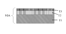
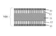
- FIG. 4 shows a polymer laminated substrate 10B of an embodiment in which a metal foil T2 is bonded to both surfaces of the polymer plate T1 and a protective film T3 is formed on each metal foil T2.
- the crystal orientation metal layers are laminated on both sides of the flexible polymer plate T1, and the protective film T3 is formed on each metal foil T2. It can be a substrate to be grown.
- a means for forming the epitaxial growth film known means such as an electrolytic plating method, an electroless plating method, a vacuum deposition method, or a sputtering film forming method can be used.
- the film thickness of the epitaxially grown film needs to be an epitaxially grown film, and is preferably 1 nm or more and 10 ⁇ m or less. This is because when the thickness of the epitaxially grown film is less than 1 nm, the adhesion of the deposited film can be ensured, and when it exceeds 10 ⁇ m, the thickness becomes excessive.
- the surface roughness of the crystallized Cu alloy foil on the polymer laminated substrate will be described. If the surface roughness of the Cu alloy foil is 40 nm or less when purchased at the surface roughness Ra, there is no problem, but there are cases where the surface roughness Ra exceeds 100 nm.
- the surface roughness (mean surface roughness) of the Cu alloy foil is 100 nm, it has sufficient performance as a substrate. However, the lower the surface roughness Ra, the better the crystal orientation, so that Ra is 100 nm. In the case of a rough surface roughness state, the surface roughness Ra is adjusted to 40 nm or less after the surface activation bonding.
- the surface roughness is preferably a mirror surface, but considering the current method and economy, it is desirable that Ra be 1 nm or more and 10 nm or less.
- a polymer laminated substrate for an excellent epitaxial growth film can be obtained, and a high-performance functional film can be formed on such a substrate.
- Examples of the present invention will be shown below, and characteristics of the obtained polymer laminated substrate will be described.
- a 200 ⁇ m wide 18 ⁇ m-thick high-pressure rolled Cu foil, a 25 ⁇ m-thick polyimide film, and a liquid crystal polymer film were bonded by a room temperature surface activation bonding method, and then heat treated at 200 ° C. for 5 minutes to obtain a polymer laminated substrate.
- Table 1 shows the ratio of the Cu (200) plane parallel to the Cu foil surface at this time, that is, the crystal orientation ratio (the diffraction peak intensity of the (200) plane of the ⁇ / 2 ⁇ diffraction peak measured by X-ray diffraction).
- the high-pressure under-rolled Cu foil has a crystal orientation ratio of 93% at a heat treatment temperature of 130 ° C. ⁇ 5 minutes, which is not sufficient, By holding at 200 ° C. for 5 minutes, the (200) plane crystal orientation ratio becomes 99% or more.
- the crystal orientation rate was 70% or less.
- ⁇ of the example in which the crystal orientation is 99% or more is 6 °, indicating a fairly high degree of biaxial crystal orientation.
- the above measured values are average values obtained by measuring a total of three points near the both ends and the center of the plate in the width direction of 200 mm, and almost no difference was observed in the values in the width direction.
- the polymer laminated substrate of the present invention is manufactured as a wide and long coil while maintaining uniform crystal orientation on the surface of the Cu foil, application as a substrate for various epitaxial growth films can be expected.
- Examples of a method for forming an epitaxial growth film include a plating method, a physical vapor deposition (PVD) method, a chemical vapor deposition (CVD) method, and a molecular beam (MBE) method.
- PVD physical vapor deposition
- CVD chemical vapor deposition
- MBE molecular beam
- the above epitaxial growth film forming method has been developed year by year.
- the substrate temperature is reduced by using RF plasma instead of the conventional method of raising the film forming substrate temperature to 400 to 800 ° C.
- a method capable of forming a film at about 200 ° C. has been developed, and low-temperature film formation of a polycrystalline Si film, GaN, or the like has become possible.
- the polymer laminated substrate according to the present invention is a polycrystalline silicon (Si) film for solar cells, a gallium nitride (GaN) film for light emitting diodes, a TiO 2 film that can be expected to have a catalyst / photoelectric effect, etc. It can be used as a substrate for various epitaxial growth films.
- the manufacturing method of the polymer laminated substrate for epitaxial growth film formation of this invention can be made into the continuous film-forming process by a reel-to-reel system by using a long coil. Furthermore, it can contribute to crystal orientation of polycrystalline silicon films for solar cells, weight reduction and flexibility, and cost reduction of GaN elements for light emitting diodes. It can be applied as a material and is extremely useful in industry.
Landscapes
- Chemical & Material Sciences (AREA)
- Engineering & Computer Science (AREA)
- Organic Chemistry (AREA)
- Materials Engineering (AREA)
- Metallurgy (AREA)
- Physics & Mathematics (AREA)
- Thermal Sciences (AREA)
- Crystallography & Structural Chemistry (AREA)
- Mechanical Engineering (AREA)
- Chemical Kinetics & Catalysis (AREA)
- Microelectronics & Electronic Packaging (AREA)
- General Chemical & Material Sciences (AREA)
- Laminated Bodies (AREA)
- Crystals, And After-Treatments Of Crystals (AREA)
- Chemical Vapour Deposition (AREA)
Abstract
Description
しかし、これら単結晶ウェハーは、サイズが大きくても300mmφ程度の切り板であり、リール・トゥ・リール方式のような連続的な生産方式での成膜はできない。
また、Siなどは強度もなく、製造工程での搬送中、ハンドリングが容易でなく注意が必要である。
また、上記単結晶ウェハーでは、基板にフレキシブル性を付与できないことから、使用する用途も限定される。
すなわち、高価な単結晶基板が使用されていること、単結晶基板はサイズも小さいこと、枚葉式の工程処理を行わなければいけないこと、基板が固く、フレキシブル性を持たせることができず、応用面が限定されていること、などである。
そこで、本発明は、上記の問題をすべて解決すべく、高度に結晶配向した表面を持つエピタキシャル成長膜形成用の高分子積層基板及びその製造方法を提供することを目的とする。
(2)本発明のエピタキシャル成長膜形成用高分子積層基板の製造方法は、高分子板の少なくとも一方の表面を活性化する工程と、圧下率90%以上で冷間圧延されたCu若しくはCu合金からなる金属箔の少なくとも一方の表面を活性化する工程と、前記高分子板の活性化表面と、前記金属箔の活性化表面を向かい合わせて積層し冷間圧延する工程と、熱処理により前記金属箔を2軸結晶配向させる工程と、を有することを特徴とする。
(3)本発明のエピタキシャル成長膜形成用高分子積層基板の製造方法は、高分子板の少なくとも一方の表面にスパッタリングにより金属層を形成する工程と、圧下率90%以上で冷間圧延されたCu若しくはCu合金からなる金属箔の少なくとも一方の表面を活性化する工程と、前記高分子板の金属層表面と、前記金属箔の活性化表面を向かい合わせて積層し冷間圧延する工程と、熱処理により前記金属箔を2軸結晶配向させる工程と、を有することを特徴とする。
(4)本発明のエピタキシャル成長膜形成用高分子積層基板の製造方法は、前記(1)又は(2)において、前記積層時の冷間圧延の圧下率は10%以下であることを特徴とする。
(5)本発明のエピタキシャル成長膜形成用高分子積層基板の製造方法は、前記(1)~(4)のいずれかにおいて、前記金属箔側表面の表面粗度をRaで1nm以上40nm以下に調整した2軸結晶配向させたことを特徴とする。
(6)本発明のエピタキシャル成長膜形成用高分子積層基板の製造方法は、前記(1)~(5)のいずれかにおいて、前記金属箔の厚みが7μm以上50μm以下のものであることを特徴とする。
(7)本発明のエピタキシャル成長膜形成用高分子積層基板の製造方法は、前記(1)~(6)のいずれかにおいて、前記熱処理温度が150℃以上400℃以下であることを特徴とする。
(8)本発明のエピタキシャル成長膜形成用高分子積層基板の製造方法は、前記(1)~(7)のいずれかにおいて、前記金属箔が、Ag、Sn、Zn、Zr、O、Nのトータルで0.01%以上1%以下含まれることを特徴とする。
(9)本発明のエピタキシャル成長膜形成用高分子積層基板の製造方法は、前記(1)~(8)のいずれかにおいて、前記高分子積層基板の製造方法により製造された高分子積層基板の金属面上に、さらに保護膜を形成することを特徴とする。
(10)本発明のエピタキシャル成長膜形成用高分子積層基板は、前記(1)~(9)のいずれかのエピタキシャル成長膜形成用高分子積層基板の製造方法により製造されたものであることを特徴とする。
図1に示すように、高分子積層基板5Aは、高分子板T1と、高分子板T1の上に積層された金属箔T2からなる。
高分子板T1としては、その使用目的によって選定されるが、貼り合わせる金属箔T2の再結晶熱処理温度150℃~400℃に耐えられるものであれば適用できるが、中でも、耐熱性に優れ、また一般に普及しているポリイミド、液晶ポリマー、アラミドなどの樹脂フィルムが、高温耐熱性に優れているので好ましく挙げられる。
Cu合金箔T2は、前もって熱処理により結晶配向させた状態で使用しても良いが、ハンドリング中、歪みが入り、結晶配向性を劣化させる危険性があるので、高分子板T1と積層して高分子積層基板としてから高度な結晶配向性を持たせることが望ましい。
圧下率90%未満であると後に行う熱処理においてCuが配向しないおそれがあるからである。
例えば日鉱マテリアルズ社製高圧下圧延Cu箔(HA箔(商品名))や日立電線社製高圧下圧延Cu箔(HX箔(商品名))などが挙げられる。
厚みは7μm以上50μm以下のものが望ましい。より好ましくは12μm~18μmである。厚みを7μm以上とする理由はCu合金箔T2の強度の確保であり、50μm以下とする理由はCu合金箔T2の加工性確保のためである。
添加元素をトータルで1%以下とする理由は、添加元素とCuは固溶体を形成しているが、トータルで1%を超えると固溶体以外の酸化物等の不純物が増加してしまい、配向に影響がでる可能性があるからである。
よって、好ましくは、トータルで0.01%以上0.1%以下である。
なお、図2に、高分子板T1の両面に金属箔T2を接合した実施形態の高分子積層基板5B示す。
図2の高分子積層基板5Bは、フレキシブルな高分子板T1の両面に結晶配向金属層が積層されているので、両面にエピタキシャル成長膜を成長させる基板とすることができる。
また、接合後にも安定な結晶配向性が得られる表面活性化接合法を用いることも望ましい。
図5に示すように、高分子板24及びCu合金箔26を、幅150mm~600mmの長尺コイルとして用意し、表面活性化接合装置D1のリコイラー部62,64のそれぞれに設置する。
リコイラー部62,64から搬送された高分子板24及びCu合金箔26は、連続的に表面活性化処理工程へ搬送され、そこで接合する2つの面を予め活性化処理した後、冷間圧接する。
不活性ガスとしては、アルゴン、ネオン、キセノン、クリプトンなどや、これらを少なくとも1種類含む混合気体を適用することができる。
例えば、青色発光ダイオード用に、エピタキシャル成長膜としてGaN膜を半導体化合物として形成する場合、InGaN層又はZnO層をCu合金箔上に保護膜として形成し、その上にGaNを成膜することができる。
保護膜の厚みは、下地のCuの拡散防止として機能させるため、0.1μm以上あればよい。また、エピタキシャル成長膜を維持するためには、10μm以下にすることが好ましい。
保護膜としての形成方法は、スパッタ法、蒸着法、CVD法、MOCVD法、電解メッキ法、無電解メッキ法など考えられるが、何れの方法でもよい。保護膜をNiなどの金属にする場合は、電解メッキ法が経済的に好ましい。また酸化物や窒化物を保護膜とする場合には、比較的基板温度が低温で成膜できるスパッタ法やMOCVD法など好ましい。
図4の高分子積層基板10Bは、フレキシブルな高分子板T1の両面に結晶配向金属層が積層され、それぞれの金属箔T2の上に保護膜T3を形成しているので、両面にエピタキシャル成長膜を成長させる基板とすることができる。
エピタキシャル成長膜の膜厚の膜厚が1nm未満の場合は成膜するものの密着性が確保できす、10μmを超える場合は過剰な厚みとなるからである。
Cu合金箔の表面粗度が購入時、表面粗度Raで40nm以下であれば問題ないが、表面粗度Raが100nmを超えるものもある。
さらに、表面活性化接合を用いて積層する場合には、積層後の加熱によっても変形等が生じる可能性が少ないので、2軸結晶配向が崩れてしまう可能性が少なく、接着剤等を用いる場合よりも有利である。
それぞれ200mm幅の18μm厚の高圧下圧延Cu箔と25μm厚のポリイミドフィルムおよび液晶ポリマーフィルムとを常温表面活性化接合法にて接合後、200℃で5分間熱処理して高分子積層基板を得た。
表1には、このときのCu(200)面がCu箔表面と平行になっている割合、つまり結晶配向率(X線回折により測定したθ/2θ回折ピークの(200)面の回折ピーク強度率:I(200)/ΣI(hkl)×100(%)))と、この(200)面が長手方向〈001〉に平行であることを表す値として2軸配向性指標のΔφ°(X線回折によるNi(111)極点図で得られるφスキャンピーク(α=35°の4本のピークの半値幅の平均値))を示す。
比較例として、熱処理を130℃で処理したとき、および一般の高圧下でない16μm厚の圧延Cu箔を前記常温活性化接合法にて接合後、200℃で5分間熱処理したときのピーク強度率を示す。
また、比較例として示す通常の圧延Cu箔を用いた場合は、熱処理しても結晶配向率は70%以下であった。
また99%以上結晶配向している実施例のΔφは6°と、かなり高度な2軸結晶配向度を示している。

さらに、太陽電池用多結晶シリコン膜の結晶配向化、軽量化やフレキシブル性の付与、発光ダイオード用GaN素子の低価格化などに寄与でき、これまで検討されていない分野でのエピタキシャル成長膜用の新素材として応用が可能となり、産業上極めて有用である。
T2 Cu箔若しくはCu合金箔
T3 保護膜
5A、5B、10A、10B 高分子積層基板
Claims (10)
- 高分子板に、圧下率90%以上で冷間圧延されたCu若しくはCu合金からなる金属箔を積層し、積層後、熱処理により前記金属箔を2軸結晶配向させることを特徴とするエピタキシャル成長膜形成用高分子積層基板の製造方法。
- 高分子板の少なくとも一方の表面を活性化する工程と、
圧下率90%以上で冷間圧延されたCu若しくはCu合金からなる金属箔の少なくとも一方の表面を活性化する工程と、
前記高分子板の活性化表面と、前記金属箔の活性化表面を向かい合わせて積層し冷間圧延する工程と、
熱処理により前記金属箔を2軸結晶配向させる工程と、を有するエピタキシャル成長膜形成用高分子積層基板の製造方法。 - 高分子板の少なくとも一方の表面にスパッタリングにより金属層を形成する工程と、
圧下率90%以上で冷間圧延されたCu若しくはCu合金からなる金属箔の少なくとも一方の表面を活性化する工程と、
前記高分子板の金属層表面と、前記金属箔の活性化表面を向かい合わせて積層し冷間圧延する工程と、
熱処理により前記金属箔を2軸結晶配向させる工程と、を有するエピタキシャル成長膜形成用高分子積層基板の製造方法。 - 前記積層時の冷間圧延の圧下率は10%以下であることを特徴とする請求項2又は3に記載のエピタキシャル成長膜形成用高分子積層基板の製造方法。
- 前記金属箔側表面の表面粗度をRaで1nm以上40nm以下に調整した2軸結晶配向させたことを特徴とする請求項1~4のいずれかに記載のエピタキシャル成長膜形成用高分子積層基板の製造方法。
- 前記金属箔の厚みが7μm以上50μm以下のものであることを特徴とする請求項1~5のいずれかに記載のエピタキシャル成長膜形成用高分子積層基板の製造方法。
- 前記熱処理温度が150℃以上400℃以下であることを特徴とする請求項1~6のいずれかに記載のエピタキシャル成長膜形成用高分子積層基板の製造方法。
- 前記金属箔が、Ag、Sn、Zn、Zr、O、Nのトータルで0.01%以上1%以下含まれることを特徴とする請求項1~7のいずれかに記載のエピタキシャル成長膜形成用高分子積層基板の製造方法。
- 前記高分子積層基板の製造方法により製造された高分子積層基板の金属面上に、さらに保護膜を形成することを特徴とする請求項1~8のいずれかに記載のエピタキシャル成長膜形成用高分子積層基板の製造方法。
- 請求項1~9のいずれかに記載のエピタキシャル成長膜形成用高分子積層基板の製造方法により製造されたエピタキシャル成長膜形成用高分子積層基板。
Priority Applications (4)
| Application Number | Priority Date | Filing Date | Title |
|---|---|---|---|
| CN2009801443447A CN102209804A (zh) | 2008-11-12 | 2009-10-20 | 磊晶成长膜形成用高分子积层基板及其制造方法 |
| JP2010537670A JP5606920B2 (ja) | 2008-11-12 | 2009-10-20 | エピタキシャル成長膜形成用高分子積層基板およびその製造方法 |
| US13/127,869 US20110290378A1 (en) | 2008-11-12 | 2009-10-20 | Polymer laminate substrate for formation of epitaxially grown film, and manufacturing method therefor |
| EP09825867A EP2366815A4 (en) | 2008-11-12 | 2009-10-20 | POLYMERLAMINATE SUBSTRATE FOR FORMING AN EPITAXIAL GROWTH FILM, AND METHOD FOR PRODUCING THEREOF |
Applications Claiming Priority (2)
| Application Number | Priority Date | Filing Date | Title |
|---|---|---|---|
| JP2008290343 | 2008-11-12 | ||
| JP2008-290343 | 2008-11-12 |
Publications (1)
| Publication Number | Publication Date |
|---|---|
| WO2010055613A1 true WO2010055613A1 (ja) | 2010-05-20 |
Family
ID=42169760
Family Applications (1)
| Application Number | Title | Priority Date | Filing Date |
|---|---|---|---|
| PCT/JP2009/005473 Ceased WO2010055613A1 (ja) | 2008-11-12 | 2009-10-20 | エピタキシャル成長膜形成用高分子積層基板およびその製造方法 |
Country Status (6)
| Country | Link |
|---|---|
| US (1) | US20110290378A1 (ja) |
| EP (1) | EP2366815A4 (ja) |
| JP (1) | JP5606920B2 (ja) |
| KR (1) | KR20110093780A (ja) |
| CN (1) | CN102209804A (ja) |
| WO (1) | WO2010055613A1 (ja) |
Cited By (1)
| Publication number | Priority date | Publication date | Assignee | Title |
|---|---|---|---|---|
| WO2021215353A1 (ja) * | 2020-04-22 | 2021-10-28 | 東洋鋼鈑株式会社 | 金属積層フィルム及びその製造方法 |
Families Citing this family (2)
| Publication number | Priority date | Publication date | Assignee | Title |
|---|---|---|---|---|
| JP2013161698A (ja) * | 2012-02-07 | 2013-08-19 | Mitsui Mining & Smelting Co Ltd | 電極箔および電子デバイス |
| WO2020008116A1 (fr) * | 2018-07-05 | 2020-01-09 | Soitec | Substrat pour un dispositif integre radioafrequence et son procede de fabrication |
Citations (11)
| Publication number | Priority date | Publication date | Assignee | Title |
|---|---|---|---|---|
| JP2003193211A (ja) * | 2001-12-27 | 2003-07-09 | Nippon Mining & Metals Co Ltd | 銅張積層板用圧延銅箔 |
| JP2004243702A (ja) * | 2003-02-14 | 2004-09-02 | Toyo Kohan Co Ltd | 合金層積層体の製造方法および合金層積層体を用いた部品の製造方法 |
| WO2004088677A1 (ja) | 2003-03-31 | 2004-10-14 | The Furukawa Electric Co., Ltd. | 酸化物超電導線材用金属基板、酸化物超電導線材及びその製造方法 |
| JP3587956B2 (ja) | 1997-06-10 | 2004-11-10 | 古河電気工業株式会社 | 酸化物超電導線材およびその製造方法 |
| JP3601830B2 (ja) | 1995-04-10 | 2004-12-15 | ユーティ―バテル エルエルシー | 効果的な2軸配向組織を有する構造体及び同構造体の製造方法 |
| JP2005324466A (ja) * | 2004-05-14 | 2005-11-24 | Toyo Kohan Co Ltd | 低熱膨張積層材および低熱膨張積層材を用いた部品 |
| JP2006286212A (ja) | 2005-03-31 | 2006-10-19 | Furukawa Electric Co Ltd:The | 酸化物超電導用高強度多結晶金属基板とそれを用いた酸化物超電導線材 |
| JP2007504305A (ja) * | 2003-09-24 | 2007-03-01 | 日東電工株式会社 | エピタキシャル有機層状構造物および製造方法 |
| JP2007200831A (ja) | 2005-12-26 | 2007-08-09 | Furukawa Electric Co Ltd:The | 超電導体用基材およびその製造方法 |
| JP2008106312A (ja) * | 2006-10-26 | 2008-05-08 | Hitachi Cable Ltd | 圧延銅箔およびその製造方法 |
| JP2008266686A (ja) * | 2007-04-17 | 2008-11-06 | Chubu Electric Power Co Inc | エピタキシャル薄膜形成用のクラッド配向金属基板及びその製造方法 |
Family Cites Families (5)
| Publication number | Priority date | Publication date | Assignee | Title |
|---|---|---|---|---|
| JP2587019B2 (ja) * | 1988-03-16 | 1997-03-05 | 第一高周波工業株式会社 | 樹脂製成型体の表面処理方法及び表面処理製品 |
| JP2002110748A (ja) * | 2000-09-28 | 2002-04-12 | Hitachi Metals Ltd | Tab用積層帯の製造方法及びtab用積層帯 |
| JP2004141918A (ja) * | 2002-10-24 | 2004-05-20 | Hitachi Metals Ltd | 積層金属板の製造方法及び積層金属板 |
| JP2007261174A (ja) * | 2006-03-29 | 2007-10-11 | Nippon Steel Chem Co Ltd | 銅張積層体の製造方法 |
| US7789977B2 (en) * | 2006-10-26 | 2010-09-07 | Hitachi Cable, Ltd. | Rolled copper foil and manufacturing method thereof |
-
2009
- 2009-10-20 KR KR1020117010375A patent/KR20110093780A/ko not_active Ceased
- 2009-10-20 CN CN2009801443447A patent/CN102209804A/zh active Pending
- 2009-10-20 WO PCT/JP2009/005473 patent/WO2010055613A1/ja not_active Ceased
- 2009-10-20 JP JP2010537670A patent/JP5606920B2/ja active Active
- 2009-10-20 EP EP09825867A patent/EP2366815A4/en not_active Withdrawn
- 2009-10-20 US US13/127,869 patent/US20110290378A1/en not_active Abandoned
Patent Citations (11)
| Publication number | Priority date | Publication date | Assignee | Title |
|---|---|---|---|---|
| JP3601830B2 (ja) | 1995-04-10 | 2004-12-15 | ユーティ―バテル エルエルシー | 効果的な2軸配向組織を有する構造体及び同構造体の製造方法 |
| JP3587956B2 (ja) | 1997-06-10 | 2004-11-10 | 古河電気工業株式会社 | 酸化物超電導線材およびその製造方法 |
| JP2003193211A (ja) * | 2001-12-27 | 2003-07-09 | Nippon Mining & Metals Co Ltd | 銅張積層板用圧延銅箔 |
| JP2004243702A (ja) * | 2003-02-14 | 2004-09-02 | Toyo Kohan Co Ltd | 合金層積層体の製造方法および合金層積層体を用いた部品の製造方法 |
| WO2004088677A1 (ja) | 2003-03-31 | 2004-10-14 | The Furukawa Electric Co., Ltd. | 酸化物超電導線材用金属基板、酸化物超電導線材及びその製造方法 |
| JP2007504305A (ja) * | 2003-09-24 | 2007-03-01 | 日東電工株式会社 | エピタキシャル有機層状構造物および製造方法 |
| JP2005324466A (ja) * | 2004-05-14 | 2005-11-24 | Toyo Kohan Co Ltd | 低熱膨張積層材および低熱膨張積層材を用いた部品 |
| JP2006286212A (ja) | 2005-03-31 | 2006-10-19 | Furukawa Electric Co Ltd:The | 酸化物超電導用高強度多結晶金属基板とそれを用いた酸化物超電導線材 |
| JP2007200831A (ja) | 2005-12-26 | 2007-08-09 | Furukawa Electric Co Ltd:The | 超電導体用基材およびその製造方法 |
| JP2008106312A (ja) * | 2006-10-26 | 2008-05-08 | Hitachi Cable Ltd | 圧延銅箔およびその製造方法 |
| JP2008266686A (ja) * | 2007-04-17 | 2008-11-06 | Chubu Electric Power Co Inc | エピタキシャル薄膜形成用のクラッド配向金属基板及びその製造方法 |
Non-Patent Citations (1)
| Title |
|---|
| See also references of EP2366815A4 |
Cited By (4)
| Publication number | Priority date | Publication date | Assignee | Title |
|---|---|---|---|---|
| WO2021215353A1 (ja) * | 2020-04-22 | 2021-10-28 | 東洋鋼鈑株式会社 | 金属積層フィルム及びその製造方法 |
| JP2021171963A (ja) * | 2020-04-22 | 2021-11-01 | 東洋鋼鈑株式会社 | 金属積層フィルム及びその製造方法 |
| CN115397664A (zh) * | 2020-04-22 | 2022-11-25 | 东洋钢钣株式会社 | 金属层叠膜及其制造方法 |
| JP7618390B2 (ja) | 2020-04-22 | 2025-01-21 | 東洋鋼鈑株式会社 | 金属積層フィルム及びその製造方法 |
Also Published As
| Publication number | Publication date |
|---|---|
| US20110290378A1 (en) | 2011-12-01 |
| CN102209804A (zh) | 2011-10-05 |
| JP5606920B2 (ja) | 2014-10-15 |
| EP2366815A4 (en) | 2012-12-26 |
| KR20110093780A (ko) | 2011-08-18 |
| JPWO2010055613A1 (ja) | 2012-04-12 |
| EP2366815A1 (en) | 2011-09-21 |
Similar Documents
| Publication | Publication Date | Title |
|---|---|---|
| JP5508280B2 (ja) | 半導体素子形成用金属積層基板の製造方法及び半導体素子形成用金属積層基板 | |
| JP5723773B2 (ja) | 酸化物超電導線材用金属積層基板の製造方法 | |
| JP5517196B2 (ja) | 超電導化合物用基板及びその製造方法 | |
| KR101258439B1 (ko) | 산화물 초전도 선재용 금속 적층 기판의 제조 방법 및 당해 기판을 이용한 산화물 초전도 선재 | |
| CN106716559B (zh) | 超导线材用基板及其制造方法、以及超导线材 | |
| JP5606920B2 (ja) | エピタキシャル成長膜形成用高分子積層基板およびその製造方法 | |
| WO2015033727A1 (ja) | 超電導線材用基板及びその製造方法、並びに超電導線材 | |
| JP5918920B2 (ja) | 超電導化合物用基板及びその製造方法 | |
| CN108138356B (zh) | 外延生长用基板及其制造方法 |
Legal Events
| Date | Code | Title | Description |
|---|---|---|---|
| WWE | Wipo information: entry into national phase |
Ref document number: 200980144344.7 Country of ref document: CN |
|
| 121 | Ep: the epo has been informed by wipo that ep was designated in this application |
Ref document number: 09825867 Country of ref document: EP Kind code of ref document: A1 |
|
| ENP | Entry into the national phase |
Ref document number: 2010537670 Country of ref document: JP Kind code of ref document: A |
|
| ENP | Entry into the national phase |
Ref document number: 20117010375 Country of ref document: KR Kind code of ref document: A |
|
| NENP | Non-entry into the national phase |
Ref country code: DE |
|
| WWE | Wipo information: entry into national phase |
Ref document number: 2009825867 Country of ref document: EP |
|
| WWE | Wipo information: entry into national phase |
Ref document number: 13127869 Country of ref document: US |