WO2010055865A1 - Couche d'enregistrement pour support d'enregistrement d'informations optique, support d'enregistrement d'informations optique et cible de pulvérisation cathodique - Google Patents
Couche d'enregistrement pour support d'enregistrement d'informations optique, support d'enregistrement d'informations optique et cible de pulvérisation cathodique Download PDFInfo
- Publication number
- WO2010055865A1 WO2010055865A1 PCT/JP2009/069222 JP2009069222W WO2010055865A1 WO 2010055865 A1 WO2010055865 A1 WO 2010055865A1 JP 2009069222 W JP2009069222 W JP 2009069222W WO 2010055865 A1 WO2010055865 A1 WO 2010055865A1
- Authority
- WO
- WIPO (PCT)
- Prior art keywords
- recording layer
- optical information
- recording
- layer
- recording medium
- Prior art date
- Legal status (The legal status is an assumption and is not a legal conclusion. Google has not performed a legal analysis and makes no representation as to the accuracy of the status listed.)
- Ceased
Links
Images
Classifications
-
- G—PHYSICS
- G11—INFORMATION STORAGE
- G11B—INFORMATION STORAGE BASED ON RELATIVE MOVEMENT BETWEEN RECORD CARRIER AND TRANSDUCER
- G11B7/00—Recording or reproducing by optical means, e.g. recording using a thermal beam of optical radiation by modifying optical properties or the physical structure, reproducing using an optical beam at lower power by sensing optical properties; Record carriers therefor
- G11B7/24—Record carriers characterised by shape, structure or physical properties, or by the selection of the material
- G11B7/241—Record carriers characterised by shape, structure or physical properties, or by the selection of the material characterised by the selection of the material
- G11B7/242—Record carriers characterised by shape, structure or physical properties, or by the selection of the material characterised by the selection of the material of recording layers
- G11B7/243—Record carriers characterised by shape, structure or physical properties, or by the selection of the material characterised by the selection of the material of recording layers comprising inorganic materials only, e.g. ablative layers
- G11B7/2437—Non-metallic elements
-
- C—CHEMISTRY; METALLURGY
- C23—COATING METALLIC MATERIAL; COATING MATERIAL WITH METALLIC MATERIAL; CHEMICAL SURFACE TREATMENT; DIFFUSION TREATMENT OF METALLIC MATERIAL; COATING BY VACUUM EVAPORATION, BY SPUTTERING, BY ION IMPLANTATION OR BY CHEMICAL VAPOUR DEPOSITION, IN GENERAL; INHIBITING CORROSION OF METALLIC MATERIAL OR INCRUSTATION IN GENERAL
- C23C—COATING METALLIC MATERIAL; COATING MATERIAL WITH METALLIC MATERIAL; SURFACE TREATMENT OF METALLIC MATERIAL BY DIFFUSION INTO THE SURFACE, BY CHEMICAL CONVERSION OR SUBSTITUTION; COATING BY VACUUM EVAPORATION, BY SPUTTERING, BY ION IMPLANTATION OR BY CHEMICAL VAPOUR DEPOSITION, IN GENERAL
- C23C14/00—Coating by vacuum evaporation, by sputtering or by ion implantation of the coating forming material
- C23C14/0021—Reactive sputtering or evaporation
- C23C14/0036—Reactive sputtering
-
- C—CHEMISTRY; METALLURGY
- C23—COATING METALLIC MATERIAL; COATING MATERIAL WITH METALLIC MATERIAL; CHEMICAL SURFACE TREATMENT; DIFFUSION TREATMENT OF METALLIC MATERIAL; COATING BY VACUUM EVAPORATION, BY SPUTTERING, BY ION IMPLANTATION OR BY CHEMICAL VAPOUR DEPOSITION, IN GENERAL; INHIBITING CORROSION OF METALLIC MATERIAL OR INCRUSTATION IN GENERAL
- C23C—COATING METALLIC MATERIAL; COATING MATERIAL WITH METALLIC MATERIAL; SURFACE TREATMENT OF METALLIC MATERIAL BY DIFFUSION INTO THE SURFACE, BY CHEMICAL CONVERSION OR SUBSTITUTION; COATING BY VACUUM EVAPORATION, BY SPUTTERING, BY ION IMPLANTATION OR BY CHEMICAL VAPOUR DEPOSITION, IN GENERAL
- C23C14/00—Coating by vacuum evaporation, by sputtering or by ion implantation of the coating forming material
- C23C14/06—Coating by vacuum evaporation, by sputtering or by ion implantation of the coating forming material characterised by the coating material
- C23C14/08—Oxides
-
- C—CHEMISTRY; METALLURGY
- C23—COATING METALLIC MATERIAL; COATING MATERIAL WITH METALLIC MATERIAL; CHEMICAL SURFACE TREATMENT; DIFFUSION TREATMENT OF METALLIC MATERIAL; COATING BY VACUUM EVAPORATION, BY SPUTTERING, BY ION IMPLANTATION OR BY CHEMICAL VAPOUR DEPOSITION, IN GENERAL; INHIBITING CORROSION OF METALLIC MATERIAL OR INCRUSTATION IN GENERAL
- C23C—COATING METALLIC MATERIAL; COATING MATERIAL WITH METALLIC MATERIAL; SURFACE TREATMENT OF METALLIC MATERIAL BY DIFFUSION INTO THE SURFACE, BY CHEMICAL CONVERSION OR SUBSTITUTION; COATING BY VACUUM EVAPORATION, BY SPUTTERING, BY ION IMPLANTATION OR BY CHEMICAL VAPOUR DEPOSITION, IN GENERAL
- C23C14/00—Coating by vacuum evaporation, by sputtering or by ion implantation of the coating forming material
- C23C14/22—Coating by vacuum evaporation, by sputtering or by ion implantation of the coating forming material characterised by the process of coating
- C23C14/34—Sputtering
- C23C14/3407—Cathode assembly for sputtering apparatus, e.g. Target
- C23C14/3414—Metallurgical or chemical aspects of target preparation, e.g. casting, powder metallurgy
-
- G—PHYSICS
- G11—INFORMATION STORAGE
- G11B—INFORMATION STORAGE BASED ON RELATIVE MOVEMENT BETWEEN RECORD CARRIER AND TRANSDUCER
- G11B7/00—Recording or reproducing by optical means, e.g. recording using a thermal beam of optical radiation by modifying optical properties or the physical structure, reproducing using an optical beam at lower power by sensing optical properties; Record carriers therefor
- G11B7/24—Record carriers characterised by shape, structure or physical properties, or by the selection of the material
- G11B7/241—Record carriers characterised by shape, structure or physical properties, or by the selection of the material characterised by the selection of the material
- G11B7/242—Record carriers characterised by shape, structure or physical properties, or by the selection of the material characterised by the selection of the material of recording layers
- G11B7/243—Record carriers characterised by shape, structure or physical properties, or by the selection of the material characterised by the selection of the material of recording layers comprising inorganic materials only, e.g. ablative layers
- G11B7/2433—Metals or elements of Groups 13, 14, 15 or 16 of the Periodic Table, e.g. B, Si, Ge, As, Sb, Bi, Se or Te
-
- G—PHYSICS
- G11—INFORMATION STORAGE
- G11B—INFORMATION STORAGE BASED ON RELATIVE MOVEMENT BETWEEN RECORD CARRIER AND TRANSDUCER
- G11B7/00—Recording or reproducing by optical means, e.g. recording using a thermal beam of optical radiation by modifying optical properties or the physical structure, reproducing using an optical beam at lower power by sensing optical properties; Record carriers therefor
- G11B7/24—Record carriers characterised by shape, structure or physical properties, or by the selection of the material
- G11B7/26—Apparatus or processes specially adapted for the manufacture of record carriers
- G11B7/266—Sputtering or spin-coating layers
-
- G—PHYSICS
- G11—INFORMATION STORAGE
- G11B—INFORMATION STORAGE BASED ON RELATIVE MOVEMENT BETWEEN RECORD CARRIER AND TRANSDUCER
- G11B7/00—Recording or reproducing by optical means, e.g. recording using a thermal beam of optical radiation by modifying optical properties or the physical structure, reproducing using an optical beam at lower power by sensing optical properties; Record carriers therefor
- G11B7/24—Record carriers characterised by shape, structure or physical properties, or by the selection of the material
- G11B7/241—Record carriers characterised by shape, structure or physical properties, or by the selection of the material characterised by the selection of the material
- G11B7/242—Record carriers characterised by shape, structure or physical properties, or by the selection of the material characterised by the selection of the material of recording layers
- G11B7/243—Record carriers characterised by shape, structure or physical properties, or by the selection of the material characterised by the selection of the material of recording layers comprising inorganic materials only, e.g. ablative layers
- G11B2007/24302—Metals or metalloids
- G11B2007/24306—Metals or metalloids transition metal elements of groups 3-10
-
- G—PHYSICS
- G11—INFORMATION STORAGE
- G11B—INFORMATION STORAGE BASED ON RELATIVE MOVEMENT BETWEEN RECORD CARRIER AND TRANSDUCER
- G11B7/00—Recording or reproducing by optical means, e.g. recording using a thermal beam of optical radiation by modifying optical properties or the physical structure, reproducing using an optical beam at lower power by sensing optical properties; Record carriers therefor
- G11B7/24—Record carriers characterised by shape, structure or physical properties, or by the selection of the material
- G11B7/241—Record carriers characterised by shape, structure or physical properties, or by the selection of the material characterised by the selection of the material
- G11B7/242—Record carriers characterised by shape, structure or physical properties, or by the selection of the material characterised by the selection of the material of recording layers
- G11B7/243—Record carriers characterised by shape, structure or physical properties, or by the selection of the material characterised by the selection of the material of recording layers comprising inorganic materials only, e.g. ablative layers
- G11B2007/24318—Non-metallic elements
- G11B2007/2432—Oxygen
-
- G—PHYSICS
- G11—INFORMATION STORAGE
- G11B—INFORMATION STORAGE BASED ON RELATIVE MOVEMENT BETWEEN RECORD CARRIER AND TRANSDUCER
- G11B7/00—Recording or reproducing by optical means, e.g. recording using a thermal beam of optical radiation by modifying optical properties or the physical structure, reproducing using an optical beam at lower power by sensing optical properties; Record carriers therefor
- G11B7/004—Recording, reproducing or erasing methods; Read, write or erase circuits therefor
- G11B7/0045—Recording
- G11B7/00452—Recording involving bubble or bump forming
Definitions
- the present invention relates to a recording layer for an optical information recording medium, an optical information recording medium, and a sputtering target useful for forming the recording layer.
- Optical information recording media are typified by optical discs such as CDs, DVDs, and BDs, and are roughly classified into three types according to the recording / reproducing method: read-only type, write once type, and rewritable type.
- the write-once type optical disc recording method mainly includes a phase change method for changing the phase of the recording layer, an interlayer reaction method for reacting a plurality of recording layers, a method for decomposing a compound constituting the recording layer, and a hole in the recording layer. It is roughly classified into a drilling method in which recording marks such as pits are locally formed.
- Patent Document 1 proposes a recording layer containing Te—OM (where M is at least one element selected from a metal element, a metalloid element, and a semiconductor element), and Patent Document 2 proposes a recording layer containing Sb and Te. Layers have been proposed.
- the first recording layer is made of an alloy containing In—O— (Ni, Mn, Mo), and the second recording layer is used.
- the second recording layer is used.
- a first recording layer a metal containing In as a main component
- a second recording layer a metal other than an oxide or a nonmetal containing at least one element belonging to Group 5B or Group 6B are stacked.
- Patent Document 5 shows a recording layer mainly composed of nitride, and recording can be performed by decomposing the nitride by heating. Materials to be performed and organic pigment materials are being studied.
- Patent Document 6 proposes an alloy formed by adding an element of 3B group, 4B group, or 5B group to an Sn alloy, and the applicant of the present application also disclosed 1 to 50 atoms of Ni and / or Co in Patent Document 7. %, A recording layer made of an Sn-based alloy is proposed.
- Patent Document 8 discloses an In alloy containing 20 to 65 atomic percent of Co, and an In alloy containing 19 atomic percent or less of one or more elements selected from Sn, Bi, Ge, and Si.
- Japanese Unexamined Patent Publication No. 2005-135568 Japanese Unexamined Patent Publication No. 2003-331461
- Japanese Unexamined Patent Publication No. 2003-326848 Japanese Patent No. 3499724 International Publication No. 2003/101750
- Pamphlet Japanese Unexamined Patent Publication No. 2002-225433 Japanese Unexamined Patent Publication No. 2007-196683 Japanese Patent No. 4110194
- optical information recording media The required characteristics required for optical information recording media are mainly that it has sufficient reflectivity for reproduction, recording with practical recording laser power (high recording sensitivity), and recording signal for reproduction. It is required to have sufficient signal amplitude (high modulation degree) and high signal strength (high C / N ratio).
- the recording material disclosed as the prior art it is difficult for the recording material disclosed as the prior art to satisfy all of the required characteristics with the recording material alone.
- the phase change method since the reflectance of the recording layer alone is low, the reflection in the optical disk state is difficult.
- a reflective film is required, and in order to increase the degree of modulation, it is necessary to provide dielectric layers such as ZnS—SiO 2 ⁇ above and below the recording layer, and the number of layers constituting the optical disk increases.
- the interlayer reaction method also requires a plurality of recording layers, the number of layers constituting the optical disk increases. For this reason, there is a problem that the number of film layers increases and productivity decreases.
- the perforation method has a high reflectivity of the recording layer itself and can secure a large degree of modulation, so that the number of layers constituting the optical disk can be reduced, but in achieving higher recording sensitivity, It turns out that further study is needed. Furthermore, durability of the recording layer (particularly durability against high temperature and high humidity) is also required.
- the present invention has been made in view of such circumstances, and an object of the present invention is to provide optical information capable of increasing the productivity of an optical information recording medium by satisfying the above required characteristics while reducing the number of layers of an optical disk.
- the object is to provide a recording layer for a recording medium, an optical information recording medium provided with the recording layer, and a sputtering target useful for forming the recording layer.
- a recording layer for an optical information recording medium on which recording is performed by laser light irradiation contains In oxide and Pd oxide, the oxide Pd contains Pd monoxide and Pd dioxide, and the ratio of Pd atoms to the total of In atoms and Pd atoms contained in the recording layer is A recording layer for an optical information recording medium of 6 to 60 atomic%.
- An optical information recording medium comprising the optical information recording medium recording layer according to any one of (1) to (4).
- An optical information recording medium comprising a recording layer on which recording is performed by laser light irradiation, and a dielectric layer formed adjacent to the recording layer, The recording layer contains In oxide and Pd oxide, the oxide Pd contains Pd monoxide and Pd dioxide, and the ratio of Pd atoms to the total of In atoms and Pd atoms contained in the recording layer is 6
- the optical information recording medium according to (6) wherein the ratio of Pd dioxide to the total of Pd monoxide and Pd contained in the recording layer is 5 to 70 mol%.
- the dielectric layer includes an oxide, a nitride, a sulfide, a carbide, or a mixture thereof.
- the oxide contained in the dielectric layer is selected from the group consisting of In, Zn, Sn, Al, Si, Ge, Ti, Ta, Nb, Hf, Zr, Cr, Bi, and Mg 1
- An oxide of at least one element, the nitride is at least one nitride of Si and Ge, the sulfide is Zn sulfide, and the carbide is selected from the group consisting of Si, Ti and W
- the optical information recording medium according to (8) which is a carbide of one or more elements.
- a sputtering target for forming a recording layer for an optical information recording medium according to any one of (1) to (4), A sputtering target consisting essentially of an In-based alloy containing 6 to 60 atomic% (preferably 6 to 50 atomic%) of Pd in a ratio of Pd atoms to the total of In atoms and Pd atoms.
- recording is performed by generating bubbles in the portion irradiated with the laser beam and changing the volume, (1) to (3)
- the recording layer for an optical information recording medium is preferable.
- the optical information recording medium of (9) above constitutes the dielectric layer, and the oxide is In, Zn, Sn, Al, Si, Ge, Ti, Ta, Nb, Hf, Zr, Cr, Bi, and Mg.
- the optical information recording medium according to (8) which is a carbide of one or more elements selected from the group consisting of W and W.
- recording is performed by generating bubbles in the portion of the recording layer irradiated with laser light and changing the volume thereof.
- the optical information recording medium is preferable.
- the sputtering target (14) is a sputtering target for forming the recording layer for an optical information recording medium according to any one of (1) to (4), wherein Pd atoms relative to the sum of In atoms and Pd atoms
- a sputtering target made of an In-based alloy containing 6 to 60 atomic% (preferably 6 to 50 atomic%) of Pd is preferable.
- a recording layer for a write once optical information recording medium having a high reflectance (initial reflectance) and excellent recording sensitivity at a practical recording laser power, and the recording layer are provided.
- a write-once optical information recording medium having excellent layer durability can be provided.
- a sputtering target useful for forming the recording layer can be provided.
- excellent recording sensitivity means a high C / N ratio (carrier-to-noise ratio, a signal at the time of reading) with a relatively low recording laser power, as will be described in detail in the section of the embodiment described later. This means that the ratio of the background noise output level) and a high degree of modulation can be realized.
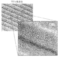
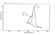
- FIG. 3 is a TEM observation photograph of the surface of the recording layer for an optical information recording medium according to the present invention. It is a Pd state analysis result (Pd 3d5 / 2 photoelectron spectrum) in Examples.
- the present inventors comprise a recording layer for a write once optical information recording medium having a higher reflectance than a conventional recording layer and excellent recording sensitivity at a practical recording laser power, and the recording layer.
- Intensive research was conducted to realize an optical information recording medium with excellent durability of the recording layer.
- the recording layer contains In oxide and Pd and the oxidation Pd contains Pd monoxide and Pd
- the oxidation layer is irradiated when the recording layer is irradiated with laser. Pd is heated by laser irradiation, decomposes and releases oxygen to change the structure of the recording layer.
- the recording method using the recording layer is different from the phase change method using the fact that the structure of the recording layer before the laser irradiation is amorphous and is amorphous after the laser irradiation. .
- the reason why the recording layer of the present invention is excellent in recording sensitivity is that the transmittance is increased (that is, the reflectance is decreased) in the portion where bubbles are generated by laser irradiation compared to the portion where bubbles are not generated. It is conceivable that the modulation degree could be increased.
- the refractive index can be increased as compared with the case where oxidized Pd is not included, and a high reflectance can be obtained. Further, since the light absorption rate of the film can be increased, the energy of the laser for signal recording can be efficiently changed to heat, and as a result, the decomposition of the oxidized Pd can be performed with a practical recording laser power. Is promoted, and the recording sensitivity can be sufficiently improved.
- the ratio of Pd atoms to the total of In atoms and Pd atoms contained in the recording layer (hereinafter sometimes referred to as “Pd amount”) needs to be 6 atomic% or more. If the amount of Pd is less than 6 atomic%, the amount of released oxygen is not sufficient because the amount of oxidized Pd that decomposes during laser irradiation is small, resulting in fewer bubbles, resulting in a lower signal intensity (C / N ratio). . Further, since the light absorption rate of the recording layer is also reduced, the laser power required for recording is increased, which is not preferable.
- the amount of Pd is preferably 8 atomic% or more, more preferably 10 atomic% or more.
- the upper limit of the amount of Pd is set to 60 atomic%.
- the upper limit of the amount of Pd is preferably 50 atomic%, more preferably 45 atomic%.
- the recording sensitivity can be improved sufficiently.
- Pd dioxide which is more unstable than monoxide Pd
- Pd dioxide is easily decomposed by laser irradiation to release oxygen, and Pd dioxide is present in the monoxide Pd that is more stable than Pd dioxide.
- the natural decomposition of Pd dioxide is suppressed and a stable recording layer can be obtained.
- the ratio of the Pd dioxide to the total of the Pd monoxide and the Pd dioxide is preferably 5 mol% or more.
- the ratio of Pd dioxide is preferably 70 mol% or less. More preferably, it is 60 mol% or less.
- the recording layer of the present invention includes an oxide of “In” in which the absolute value of the standard free energy of formation of oxide with respect to 1 mol of oxygen is larger than Pd together with the above-described oxide Pd.
- In oxide which is more stable than oxidized Pd, together with oxidized Pd, the change in form due to oxygen release when the oxidized Pd is decomposed can be made clear and large, and the recording sensitivity can be improved sufficiently. Can be made.
- the recording layer of the present invention contains In oxide, and preferably contains 50 mol% or more of In oxide.
- the recording layer of the present invention may contain unavoidable impurities in addition to the oxidized In and oxidized Pd.
- Sn, Al, Bi, Cu, Nb, Ti, Si, and Ta are contained within a total amount of about 30 atomic% or less in the state of oxide or metal for the purpose of improving the absorptance and controlling the refractive index. You may go out.
- the thickness of the recording layer depends on the structure of the optical information recording medium, such as inserting other layers such as a metal compound layer and a metal layer above and below the recording layer, but when the recording layer is used as a single layer (dielectric) Whether the body layer or the optical adjustment layer is not provided) or not, the thickness of the recording layer is preferably 5 to 100 nm.
- the film thickness of the recording layer is smaller than 5 nm, there is a tendency that a sufficient change in reflectance due to recording is difficult to obtain. More preferably, it is 10 nm or more, More preferably, it is 20 nm or more, Most preferably, it is 25 nm or more.
- the film thickness of the recording layer is larger than 100 nm, it takes time to form the film, the productivity is lowered, and the laser power required for recording tends to increase. More preferably, it is 70 nm or less, More preferably, it is 60 nm or less.
- the recording layer of the present invention contains oxidized Pd (for example, PdO, PdO 2, PdOX, etc.).
- the recording layer can be formed by sputtering.
- the sputtering method is preferable because the film thickness distribution uniformity within the disk surface can be secured.
- the ratio of the oxygen flow rate to the Ar (argon) flow rate is 0.5 to 10.0 as sputtering conditions.
- Other conditions in the sputtering method are not particularly limited, and a widely used method can be adopted.
- the gas pressure is in the range of 0.1 to 1.0 Pa, for example, and the sputtering power is in the range of 0.5 to 20 W / cm 2 , for example. What is necessary is just to control to a range.
- target As a sputtering target (hereinafter, simply referred to as “target”) used in the sputtering method, (A) Indium oxide (specifically, for example, containing 50 mol% or more of oxidized In) and Pd (eg, oxidized Pd and / or metal Pd), and with respect to the sum of In atoms and Pd atoms contained in the sputtering target A sputtering target characterized in that the ratio of Pd atoms is 6 to 60 atomic%, (B) A sputtering target having a feature in that it is made of an In-based alloy containing 6 to 60 atomic% of Pd (for example, metal Pd) in the ratio of Pd atoms to the total of In atoms and Pd atoms can be mentioned. Also, (C) A metal In target (pure In metal target) and a metal Pd target (pure Pd metal target) are used, and these are simultaneously discharged to perform multi-source sputtering
- the sputtering target of the above (A) in particular, it is possible to use a product obtained by mixing and sintering powders of oxidized In and metal Pd, and in-plane uniformity of productivity and composition of the formed thin film. It is preferable in terms of thickness control.
- the component composition of the sputtering target of the present invention does not prescribe even the trace components that are inevitably mixed, and the trace amounts of these unavoidable impurities are allowed as long as the above characteristics of the present invention are not impaired.
- the optical information recording medium of the present invention is characterized in that the recording layer is provided.
- the configuration other than the recording layer is not particularly limited, and a configuration known in the field of optical information recording media is adopted. It is also possible to provide the recording layer and the following dielectric layer formed adjacent to the recording layer.
- the optical information recording medium of the present invention has a recording layer exhibiting the above excellent characteristics, but it is also necessary to maintain the above excellent characteristics even in a high temperature and high humidity environment, that is, to ensure excellent durability. It is. Under the above environment, the oxidized Pd in the portion not irradiated with laser (that is, recording is not performed) is gradually reduced to release oxygen, resulting in a change in optical characteristics and a decrease in reflectance. Appearance is considered as a cause of the decrease in durability. However, it seems that by forming the dielectric layer adjacent to the recording layer, unnecessary decomposition of oxidized Pd (particularly Pd dioxide) in the recording layer can be suppressed and stably held.
- the above-mentioned “formation of the dielectric layer adjacent to the recording layer” includes, for example, the case where the dielectric layer is formed between the substrate and the recording layer and adjacent to the recording layer, and / or the recording layer and will be described later. A case where it is formed between the light transmission layer and adjacent to the recording layer can be mentioned.
- the dielectric layer also improves durability by acting as an oxygen barrier layer. By preventing the escape of oxygen that can be caused by unnecessary decomposition of the oxidized Pd, it is possible to prevent a change in reflectance (particularly, a decrease in reflectance), and to secure the reflectance necessary for the recording layer.
- recording characteristics can be improved by forming a dielectric layer. This is because the thermal diffusion of the laser incident by the dielectric layer is optimally controlled to prevent the bubbles in the recording portion from becoming too large or the decomposition of the oxidized Pd from proceeding too much to collapse the bubbles. This is considered to be possible to optimize.
- Examples of the material of the dielectric layer include oxides, nitrides, sulfides, carbides, fluorides, or mixtures thereof.
- Examples of the oxides include In, Zn, Sn, Al, Si, Ge, Ti, and Ta.
- the nitride is a nitride of one or more elements selected from the group consisting of In, Sn, Ge, Cr, Si, Al, Nb, Mo, Ti, and Zn (preferably Si and / or Ge nitridation).
- sulfides include Zn sulfide.
- the carbide is a carbide of one or more elements selected from the group consisting of In, Sn, Ge, Cr, Si, Al, Ti, Zr, Ta and W (preferably from the group consisting of Si, Ti and W).
- the carbide of one or more elements selected) and the fluoride include a fluoride of one or more elements selected from the group consisting of Si, Al, Mg, Ca, and La. Examples of such a mixture include ZnS—SiO2.
- the above compound (oxide or the like) containing at least one of In, Zn, Sn, Al, Si, Ti, and Mg, or a mixture thereof, and more preferable is In, Zn, Sn, The above-mentioned compound containing any one or more elements of Al or a mixture thereof.
- the film thickness of the dielectric layer is preferably 2 to 40 nm. This is because if the thickness is less than 2 nm, the effect of the dielectric layer (particularly, the effect as an oxygen barrier) is hardly exhibited. More preferably, it is 3 nm or more. On the other hand, if the dielectric layer is too thick, it is difficult for the recording layer to change (generate bubbles) due to laser irradiation, and the recording characteristics may be deteriorated. Therefore, the thickness of the dielectric layer is preferably 40 nm or less, more preferably 35 nm or less.
- the present invention does not define the method for forming the dielectric layer, but it is preferable to form the dielectric layer by the sputtering method as in the recording layer.
- the sputtering conditions are Ar flow rate, for example, in the range of 10 to 100 sccm, and when using a metal target as described below, the oxygen flow rate during oxide layer formation is For example, the range is 5 to 60 sccm, and the nitrogen flow rate when forming the nitride layer is, for example, 5 to 80 sccm.
- the gas pressure may be in the range of 0.1 to 1.0 Pa, and the sputtering power may be in the range of 0.5 to 50 W / cm 2, for example.
- a sputtering target used for forming the dielectric layer in addition to a target made of the above compound (oxide, nitride, sulfide, carbide, fluoride), other than oxygen, nitrogen, sulfur, carbon, fluorine in the compound
- a metal target containing a constituent element a target made of a pure metal or an alloy
- the configuration other than the recording layer and the dielectric layer is not particularly limited, and a configuration known in the field of optical information recording media can be adopted.
- optical information recording medium As an optical information recording medium (optical disk), a structure in which a recording layer is laminated on a substrate in which a laser guide groove is engraved, and a light transmission layer is further laminated on the substrate.
- examples of the material of the substrate include polycarbonate resin, norbornene resin, cyclic olefin copolymer, and amorphous polyolefin.
- the light transmission layer polycarbonate or ultraviolet curable resin can be used.
- the light transmission layer it is preferable that the light transmission layer has a high transmittance with respect to a laser for recording and reproduction, and has a small light absorption rate.
- the thickness of the substrate is, for example, 0.5 mm to 1.2 mm. In addition, the thickness of the light transmission layer is, for example, 0.1 mm to 1.2 mm.
- the recording layer of the present invention exhibits high reflectivity and exhibits excellent recording characteristics by itself.
- the recording layer may be above and / or below the recording layer to improve the durability of the recording layer.
- an oxide layer, a sulfide layer, a metal layer, or the like may be provided. By laminating these layers, it is possible to suppress oxidation and decomposition, which are deterioration with time of the recording layer.
- an optical adjustment layer or a dielectric layer may be provided between the substrate and the recording layer in order to further increase the reflectivity of the optical disk. Examples of the material of the optical adjustment layer include Ag, Au, Cu, Al, Ni, Cr, Ti, and alloys thereof.
- a single-layer optical disc in which one recording layer and one light transmission layer are formed is shown.
- the present invention is not limited to this, and two or more optical discs in which a plurality of recording layers and light transmission layers are stacked are shown. It may be.
- a transparent intermediate layer made of a transparent resin or the like may be included.
- a feature of the present invention is that the recording layer described above is employed.
- the optical information recording medium may be manufactured by being formed by a usual method without being particularly limited.
- the present invention is also characterized in that the recording layer described above is employed and a dielectric layer is formed adjacent to the recording layer.
- a substrate other than the recording layer and the dielectric layer and light transmission There is no particular limitation on the method of forming the layer, and further, the optical adjustment layer, the transparent intermediate layer, etc., and the optical information recording medium may be produced by forming it by a conventional method.
- optical information recording medium examples include CD, DVD, and BD.
- a BD capable of recording and reproducing data by irradiating a recording layer with blue laser light having a wavelength of about 380 nm to 450 nm, preferably about 405 nm.
- a specific example is -R.
- Example 1 Production of optical disk A polycarbonate substrate (thickness: 1.1 mm, diameter: 120 mm, track pitch: 0.32 ⁇ m, groove depth: 25 nm) was used as a disk substrate, and a DC magnetron sputtering method was used on the substrate. As shown in Table 1, recording layers having various amounts of Pd were formed. The film thickness of the recording layer was 40 nm. Sputtering was performed by simultaneously discharging a pure In metal target and a pure Pd metal target.
- the sputtering conditions for forming the recording layer were Ar flow rate: 10 sccm, oxygen flow rate: 10 sccm, gas pressure: 0.4 Pa, DC sputtering power: 100 to 200 W, and substrate temperature: room temperature.
- the component composition (Pd amount) of the formed recording layer was measured by ICP emission analysis, fluorescent X-ray analysis, or X-ray photoelectron spectroscopy.
- an ultraviolet curable resin (“BRD-864” manufactured by Nippon Kayaku Co., Ltd.) was spin-coated on the recording layer obtained as described above, and then irradiated with ultraviolet rays to have a film thickness of about 0.1 mm. A light transmission layer was formed to obtain an optical disk.
- optical disk evaluation device manufactured by Pulstec Industrial Co., Ltd., recording laser wavelength: 405 nm, NA (numerical aperture): 0.85
- the laser is irradiated onto the track and converted from the return intensity of the reflected light.
- the reflectance at a wavelength of 405 nm was determined.
- recording laser power in the range of 2 mW to 20 mW, linear velocity: 4.92 m / s, length: 0.60 ⁇ m, recording mark (Blu-ray Disc 8T signal) was repeatedly formed.
- the degree of modulation was calculated from the following formula (1) by determining the reflectance of the unrecorded portion and the reflectance of the recorded portion.
- Modulation degree (change rate of reflectance) (reflectance of unrecorded portion ⁇ reflectance of recorded portion) / (reflectance of unrecorded portion) (1)
- the reflectance is 4% or more
- the recording power (recording laser power when the highest C / N ratio is obtained) is 9 mW or less
- the C / N ratio (the highest C / N ratio) is 45 dB or more.
- those having a modulation degree of 0.40 or more were evaluated as having high reflectivity (initial reflectivity) and excellent recording sensitivity with practical recording laser power.
- the recording layer satisfying the definition of the present invention has a high reflectance and a high recording sensitivity even when the recording laser power is low.
- Example 2 An optical disc was produced and evaluated in the same manner as in Experimental Example 1 except that a recording layer having the component composition shown in Table 2 below was formed using pure Cu or pure Ag instead of pure Pd as a sputtering target. The results are shown in Table 2.
- Example 3 Except for changing the film forming gas flow rate during film formation as shown in Table 3 below, in the same manner as in Experimental Example 1, No. 1 in Table 3 was obtained. 2 optical disks were prepared and evaluated. The results are shown in Table 3. In Table 3, No. 1 is No. 1 in Table 1. Same as 5.
- Table 3 shows that the amount of oxygen contained in the recording layer is small and In and Pd are not sufficiently oxidized (No. 2), and the amount of oxygen contained in the recording layer is No. 2. No. 2 more than 2. No. 1 is compared with each other when recording is performed with the same recording power. In case of 2, there was a problem that a sufficient C / N ratio and modulation degree could not be obtained.
- FIG. 1 a TEM observation photograph of the surface of the recording layer after laser irradiation was taken with respect to those having good recording characteristics satisfying the provisions of the present invention.
- the TEM observation photograph is shown in FIG.
- FIG. 1 particularly, enlarged photograph
- those satisfying the provisions of the present invention have sufficient recording sensitivity because, as described above, the oxidized Pd in the recording layer decomposes to generate oxygen and bubbles are generated. It seems to have been raised.
- Example 4 (1) Production of optical disk A polycarbonate substrate (thickness: 1.1 mm, diameter: 120 mm, track pitch: 0.32 ⁇ m, groove depth: 25 nm) was used as a disk substrate, and a DC magnetron sputtering method was used on the substrate. Recording layers having various contents of In oxide, metal Pd, and oxide Pd (the molar ratio of Pd monoxide and Pd in the total of Pd monoxide and Pd dioxide is as shown in Table 4) did. The film thickness of the recording layer was 40 nm. Sputtering was performed by multi-source sputtering by simultaneous discharge of two targets, a pure In metal target and a pure Pd metal target.
- the sputtering conditions for forming the recording layer were constant at Ar flow rate: 10 sccm, and the oxygen flow rate introduced simultaneously with Ar was changed within the range of 5 to 50 sccm as shown in Table 4.
- the gas pressure was 0.4 Pa
- the DC sputtering power was 100 to 200 W
- the substrate temperature was room temperature.
- the component composition (Pd amount) of the formed recording layer was measured by ICP emission analysis, fluorescent X-ray analysis, or X-ray photoelectron spectroscopy.
- an ultraviolet curable resin (“BRD-864” manufactured by Nippon Kayaku Co., Ltd.) is spin-coated on the obtained recording layer, and then irradiated with ultraviolet rays to form a light transmission layer having a thickness of about 0.1 mm. Film was obtained to obtain an optical disk.
- the state analysis of Pd was performed as follows. That is, the outermost surface spectrum of the recording layer is measured by X-ray photoelectron spectroscopy (the apparatus is a Quanta SXM manufactured by Physical Electronics Co., Ltd.), and the peak separation of the Pd 3d5 / 2 photoelectron spectrum is performed. Presence form of Pd present in: The molar ratio (mol%) of metal Pd, monoxide Pd, and Pd dioxide was determined. The charge was corrected using photoelectrons from the C1s level as a reference. The analysis was performed in a state where the light transmission layer (cover layer) of the optical disc was peeled off and a recording layer was formed on the polycarbonate substrate, and the analysis region was about ⁇ 200 ⁇ m. As an example of the spectrum, No. The Pd ⁇ 3d5 / 2 photoelectron spectrum of No. 4 is shown in FIG.
- optical disc evaluation apparatus (“ODU-1000” manufactured by Pulstec Industrial Co., Ltd.) was used, a recording laser center wavelength was set to 405 nm, and a lens with NA (numerical aperture): 0.85 was used.
- NA number of NA
- Modulation degree (change rate of reflectance) (reflectance of unrecorded portion ⁇ reflectance of recorded portion) / (reflectance of unrecorded portion) (1)
- the degree of modulation is increased by the presence of Pd dioxide as the oxidized Pd, and in particular, the ratio of Pd dioxide to the total of Pd monoxide and Pd dioxide is within the recommended range. It can be seen that a high degree of modulation can be obtained. No. In No. 6, the recording power and the modulation degree could not be measured, but barely recorded, the recording power was 5.5 mW and the modulation degree was 0.15.
- Example 5 Production of optical disk A polycarbonate substrate (thickness: 1.1 mm, diameter: 120 mm, track pitch: 0.32 ⁇ m, groove depth: 25 nm) was used as a disk substrate. And in Table 5 below, No. For 3 to 5 and 9 to 12, a dielectric layer (lower) having the components and film thicknesses shown in Table 5 was formed by DC magnetron sputtering using an oxide target or a pure metal target.
- the sputtering conditions for forming this dielectric layer are: Ar flow rate: 10-30 sccm, oxygen flow rate (when using a pure metal target as a target): 0-10 sccm, gas pressure: 0.2-0.4 Pa, DC sputtering power: 100 to 400 W, substrate temperature: room temperature.
- a recording layer was formed.
- recording layers having a ratio of In atoms to Pd atoms of 60:40 were formed on the dielectric layer (lower) by a DC magnetron sputtering method.
- the film thickness of the recording layer was 40 nm.
- Sputtering was performed by multi-source sputtering by simultaneous discharge of two targets, a pure In metal target and a pure Pd metal target.
- the sputtering conditions for forming the recording layer were Ar flow rate: 10 sccm, oxygen flow rate: 15 sccm, gas pressure: 0.4 Pa, DC sputtering power: 100 to 200 W, and substrate temperature: room temperature.
- an oxide target or a pure metal target for example, ZnS—SiO 2 metal, metal Mg, metal Zn, metal Sn, metal Bi, metal Ti, etc. as a target
- a dielectric layer (upper) having the components and film thicknesses shown in Table 5 was formed.
- an ultraviolet curable resin (“BRD-864” manufactured by Nippon Kayaku Co., Ltd.) is spin-coated on the dielectric layer (top), and then irradiated with ultraviolet rays to transmit light having a thickness of about 0.1 mm. A layer was formed to obtain an optical disk.
- the recording layer contains oxidized In and oxidized Pd, and the oxidized Pd contains oxidized Pd and oxidized Pd.
- the ratio of oxidized Pd to the total of oxidized Pd and oxidized Pd is 27.8. It was confirmed separately that it was mol%.
- the Pd state analysis was performed as follows. That is, the outermost surface spectrum of the recording layer was measured by X-ray photoelectron spectroscopy (the apparatus was Quantera SXM manufactured by Physical Electronics), and the peak separation of the Pd 3d5 / 2 photoelectron spectrum was performed. Presence form of Pd present in: The molar ratio (mol%) of metal Pd, monoxide Pd, and Pd dioxide was determined. The charge was corrected using photoelectrons from the C1s level as a reference. The analysis area was about ⁇ 200 ⁇ m.
- optical disk evaluation apparatus manufactured by Pulstec Industrial Co., Ltd., recording laser wavelength: 405 nm, NA (numerical aperture): 0.85
- the laser is irradiated onto the track, and the laser beam of the unrecorded portion of the optical disk
- the reflectance (initial reflectance) at a wavelength of 405 nm was determined in terms of the return light intensity.
- Rate of change in reflectance (%) 100 ⁇ (reflectance after test [%] ⁇ initial reflectance [%]) / initial reflectance [%] (2)
- the change in reflectance can be made sufficiently smaller than when the dielectric layer is not formed, and an optical information recording medium excellent in durability can be obtained. It can be seen that it can be realized. In particular, it can be seen that by forming the dielectric layer above and below the recording layer, the rate of change in reflectivity is remarkably reduced and the durability is excellent.
- a recording layer for a write once optical information recording medium having a high reflectance (initial reflectance) and excellent recording sensitivity at a practical recording laser power, and the recording layer are provided.
- a write-once optical information recording medium having excellent layer durability can be provided.
- a sputtering target useful for forming the recording layer can be provided.
Landscapes
- Chemical & Material Sciences (AREA)
- Engineering & Computer Science (AREA)
- Chemical Kinetics & Catalysis (AREA)
- Materials Engineering (AREA)
- Mechanical Engineering (AREA)
- Metallurgy (AREA)
- Organic Chemistry (AREA)
- Inorganic Chemistry (AREA)
- Manufacturing & Machinery (AREA)
- Optical Record Carriers And Manufacture Thereof (AREA)
- Thermal Transfer Or Thermal Recording In General (AREA)
Abstract
L'invention porte sur une couche d'enregistrement pour un support d'enregistrement d'informations optique, laquelle couche a un facteur de réflexion (facteur de réflexion initial) élevé et d'excellentes caractéristiques d'enregistrement ; sur un support d'enregistrement d'informations optique comprenant la couche d'enregistrement ; et sur une cible de pulvérisation cathodique utile pour former la couche d'enregistrement. La couche d'enregistrement pour un support d'enregistrement d'informations optique, sur lequel un enregistrement est effectué par rayonnement d'une lumière laser, est caractérisée en ce qu'elle contient de l'oxyde d'indium (In) et de l'oxyde de palladium (Pd) qui comprend le monoxyde de palladium et le dioxyde de palladium. La couche d'enregistrement pour un support d'enregistrement d'informations optique est également caractérisée en ce que le rapport des atomes de Pd contenus dans la couche d'enregistrement au total des atomes d'In et des atomes de Pd contenus dans celle-ci est de 6-60 % en pourcentage atomique.
Priority Applications (1)
| Application Number | Priority Date | Filing Date | Title |
|---|---|---|---|
| US13/127,994 US8354155B2 (en) | 2008-11-12 | 2009-11-11 | Recording layer for optical information recording medium, optical information recording medium, and sputtering target |
Applications Claiming Priority (6)
| Application Number | Priority Date | Filing Date | Title |
|---|---|---|---|
| JP2008-290309 | 2008-11-12 | ||
| JP2008290309 | 2008-11-12 | ||
| JP2009217291A JP4969624B2 (ja) | 2008-11-12 | 2009-09-18 | 光情報記録媒体 |
| JP2009217292A JP4969625B2 (ja) | 2008-11-12 | 2009-09-18 | 光情報記録媒体 |
| JP2009-217292 | 2009-09-18 | ||
| JP2009-217291 | 2009-09-18 |
Publications (1)
| Publication Number | Publication Date |
|---|---|
| WO2010055865A1 true WO2010055865A1 (fr) | 2010-05-20 |
Family
ID=42169997
Family Applications (1)
| Application Number | Title | Priority Date | Filing Date |
|---|---|---|---|
| PCT/JP2009/069222 Ceased WO2010055865A1 (fr) | 2008-11-12 | 2009-11-11 | Couche d'enregistrement pour support d'enregistrement d'informations optique, support d'enregistrement d'informations optique et cible de pulvérisation cathodique |
Country Status (1)
| Country | Link |
|---|---|
| WO (1) | WO2010055865A1 (fr) |
Cited By (3)
| Publication number | Priority date | Publication date | Assignee | Title |
|---|---|---|---|---|
| WO2011034188A1 (fr) * | 2009-09-18 | 2011-03-24 | 株式会社神戸製鋼所 | Couche d'enregistrement pour support d'enregistrement d'informations optiques, support d'enregistrement d'informations optiques et cible de pulvérisation |
| WO2011034153A1 (fr) * | 2009-09-18 | 2011-03-24 | 株式会社神戸製鋼所 | Couche d'enregistrement pour support d'enregistrement d'information optique, support d'enregistrement d'information optique et cible de pulvérisation cathodique |
| WO2011132371A1 (fr) * | 2010-04-19 | 2011-10-27 | ソニー株式会社 | Support d'enregistrement optique |
Citations (4)
| Publication number | Priority date | Publication date | Assignee | Title |
|---|---|---|---|---|
| JP2003326848A (ja) * | 2002-05-10 | 2003-11-19 | Ricoh Co Ltd | 追記型光記録媒体 |
| JP2005314734A (ja) * | 2004-04-28 | 2005-11-10 | Idemitsu Kosan Co Ltd | スパッタリングターゲット及び透明導電膜及び透明導電ガラス基板 |
| JP2007230207A (ja) * | 2006-02-03 | 2007-09-13 | Kobe Steel Ltd | 光情報記録媒体用記録層および光情報記録媒体、並びにスパッタリング・ターゲット |
| JP2008302688A (ja) * | 2006-12-20 | 2008-12-18 | Kobe Steel Ltd | 光情報記録媒体 |
-
2009
- 2009-11-11 WO PCT/JP2009/069222 patent/WO2010055865A1/fr not_active Ceased
Patent Citations (4)
| Publication number | Priority date | Publication date | Assignee | Title |
|---|---|---|---|---|
| JP2003326848A (ja) * | 2002-05-10 | 2003-11-19 | Ricoh Co Ltd | 追記型光記録媒体 |
| JP2005314734A (ja) * | 2004-04-28 | 2005-11-10 | Idemitsu Kosan Co Ltd | スパッタリングターゲット及び透明導電膜及び透明導電ガラス基板 |
| JP2007230207A (ja) * | 2006-02-03 | 2007-09-13 | Kobe Steel Ltd | 光情報記録媒体用記録層および光情報記録媒体、並びにスパッタリング・ターゲット |
| JP2008302688A (ja) * | 2006-12-20 | 2008-12-18 | Kobe Steel Ltd | 光情報記録媒体 |
Cited By (7)
| Publication number | Priority date | Publication date | Assignee | Title |
|---|---|---|---|---|
| WO2011034188A1 (fr) * | 2009-09-18 | 2011-03-24 | 株式会社神戸製鋼所 | Couche d'enregistrement pour support d'enregistrement d'informations optiques, support d'enregistrement d'informations optiques et cible de pulvérisation |
| WO2011034153A1 (fr) * | 2009-09-18 | 2011-03-24 | 株式会社神戸製鋼所 | Couche d'enregistrement pour support d'enregistrement d'information optique, support d'enregistrement d'information optique et cible de pulvérisation cathodique |
| US8530024B2 (en) | 2009-09-18 | 2013-09-10 | Kobe Steel, Ltd. | Recording layer for optical information recording medium, optical information recording medium, and sputtering target |
| US8597757B2 (en) | 2009-09-18 | 2013-12-03 | Kobe Steel, Ltd. | Recording layer for optical information recording medium, optical information recording medium, and sputtering target |
| WO2011132371A1 (fr) * | 2010-04-19 | 2011-10-27 | ソニー株式会社 | Support d'enregistrement optique |
| JP2011243270A (ja) * | 2010-04-19 | 2011-12-01 | Sony Corp | 光記録媒体 |
| US8685517B2 (en) | 2010-04-19 | 2014-04-01 | Sony Corporation | Optical recording medium |
Similar Documents
| Publication | Publication Date | Title |
|---|---|---|
| JP4969624B2 (ja) | 光情報記録媒体 | |
| WO2011034153A1 (fr) | Couche d'enregistrement pour support d'enregistrement d'information optique, support d'enregistrement d'information optique et cible de pulvérisation cathodique | |
| JP5346915B2 (ja) | 光情報記録媒体用記録層、及び光情報記録媒体 | |
| JP5662874B2 (ja) | 光情報記録媒体用記録膜および光情報記録媒体、並びに上記記録膜の形成に用いられるスパッタリングターゲット | |
| JP5399836B2 (ja) | 光情報記録媒体用記録層、光情報記録媒体およびスパッタリングターゲット | |
| WO2010055865A1 (fr) | Couche d'enregistrement pour support d'enregistrement d'informations optique, support d'enregistrement d'informations optique et cible de pulvérisation cathodique | |
| JP5276557B2 (ja) | 光情報記録媒体用記録層および光情報記録媒体 | |
| JP5399184B2 (ja) | 光情報記録媒体およびスパッタリングターゲット | |
| WO2021117470A1 (fr) | Couche d'enregistrement pour support d'enregistrement d'informations optique, support d'enregistrement d'informations optique, et cible de pulvérisation cathodique | |
| JP2008217957A (ja) | 光情報記録媒体 | |
| JP7130447B2 (ja) | 光情報記録媒体用記録層、光情報記録媒体、及びスパッタリングターゲット | |
| JP6781679B2 (ja) | 記録層、光情報記録媒体及びスパッタリングターゲット | |
| JP2012020530A (ja) | 光情報記録媒体用記録層、光情報記録媒体、およびスパッタリングターゲット | |
| JP2009196312A (ja) | 光情報記録媒体用記録層、および光情報記録媒体、ならびに光情報記録媒体の記録層形成用スパッタリングターゲット |
Legal Events
| Date | Code | Title | Description |
|---|---|---|---|
| 121 | Ep: the epo has been informed by wipo that ep was designated in this application |
Ref document number: 09826112 Country of ref document: EP Kind code of ref document: A1 |
|
| WWE | Wipo information: entry into national phase |
Ref document number: 13127994 Country of ref document: US |
|
| NENP | Non-entry into the national phase |
Ref country code: DE |
|
| 122 | Ep: pct application non-entry in european phase |
Ref document number: 09826112 Country of ref document: EP Kind code of ref document: A1 |