WO2010087288A1 - 固体撮像装置 - Google Patents
固体撮像装置 Download PDFInfo
- Publication number
- WO2010087288A1 WO2010087288A1 PCT/JP2010/050818 JP2010050818W WO2010087288A1 WO 2010087288 A1 WO2010087288 A1 WO 2010087288A1 JP 2010050818 W JP2010050818 W JP 2010050818W WO 2010087288 A1 WO2010087288 A1 WO 2010087288A1
- Authority
- WO
- WIPO (PCT)
- Prior art keywords
- register unit
- multiplication
- unit
- charge
- state imaging
- Prior art date
- Legal status (The legal status is an assumption and is not a legal conclusion. Google has not performed a legal analysis and makes no representation as to the accuracy of the status listed.)
- Ceased
Links
Images





Classifications
-
- H—ELECTRICITY
- H10—SEMICONDUCTOR DEVICES; ELECTRIC SOLID-STATE DEVICES NOT OTHERWISE PROVIDED FOR
- H10F—INORGANIC SEMICONDUCTOR DEVICES SENSITIVE TO INFRARED RADIATION, LIGHT, ELECTROMAGNETIC RADIATION OF SHORTER WAVELENGTH OR CORPUSCULAR RADIATION
- H10F39/00—Integrated devices, or assemblies of multiple devices, comprising at least one element covered by group H10F30/00, e.g. radiation detectors comprising photodiode arrays
- H10F39/10—Integrated devices
- H10F39/12—Image sensors
- H10F39/15—Charge-coupled device [CCD] image sensors
-
- H—ELECTRICITY
- H04—ELECTRIC COMMUNICATION TECHNIQUE
- H04N—PICTORIAL COMMUNICATION, e.g. TELEVISION
- H04N25/00—Circuitry of solid-state image sensors [SSIS]; Control thereof
-
- H—ELECTRICITY
- H04—ELECTRIC COMMUNICATION TECHNIQUE
- H04N—PICTORIAL COMMUNICATION, e.g. TELEVISION
- H04N25/00—Circuitry of solid-state image sensors [SSIS]; Control thereof
- H04N25/70—SSIS architectures; Circuits associated therewith
- H04N25/71—Charge-coupled device [CCD] sensors; Charge-transfer registers specially adapted for CCD sensors
- H04N25/713—Transfer or readout registers; Split readout registers or multiple readout registers
-
- H—ELECTRICITY
- H10—SEMICONDUCTOR DEVICES; ELECTRIC SOLID-STATE DEVICES NOT OTHERWISE PROVIDED FOR
- H10F—INORGANIC SEMICONDUCTOR DEVICES SENSITIVE TO INFRARED RADIATION, LIGHT, ELECTROMAGNETIC RADIATION OF SHORTER WAVELENGTH OR CORPUSCULAR RADIATION
- H10F39/00—Integrated devices, or assemblies of multiple devices, comprising at least one element covered by group H10F30/00, e.g. radiation detectors comprising photodiode arrays
- H10F39/10—Integrated devices
- H10F39/12—Image sensors
- H10F39/15—Charge-coupled device [CCD] image sensors
- H10F39/151—Geometry or disposition of pixel elements, address lines or gate electrodes
-
- H—ELECTRICITY
- H10—SEMICONDUCTOR DEVICES; ELECTRIC SOLID-STATE DEVICES NOT OTHERWISE PROVIDED FOR
- H10F—INORGANIC SEMICONDUCTOR DEVICES SENSITIVE TO INFRARED RADIATION, LIGHT, ELECTROMAGNETIC RADIATION OF SHORTER WAVELENGTH OR CORPUSCULAR RADIATION
- H10F39/00—Integrated devices, or assemblies of multiple devices, comprising at least one element covered by group H10F30/00, e.g. radiation detectors comprising photodiode arrays
- H10F39/80—Constructional details of image sensors
- H10F39/803—Pixels having integrated switching, control, storage or amplification elements
Definitions
- the present invention relates to a charge multiplying solid-state imaging device such as an EM-CCD.
- a CCD Charge-Coupled Device
- EM-CCD Electro CCD
- Multiplying (-CCD)
- This type of solid-state imaging device includes a plurality of photodiodes and the like, and in addition to an imaging region that generates charges according to the amount of incident light and an output register unit that reads the charges in the imaging region, the read charges are multiplied.
- a multiplication register section is provided, and a weak light image can be captured by using the charge multiplication action of the multiplication register section.
- Patent Documents 1 and 2 disclose this type of solid-state imaging device.
- the solid-state imaging devices described in Patent Documents 1 and 2 control the multiplication factor (gain) of the multiplication register unit based on the output of the multiplication register unit, that is, feedback control of the multiplication factor of the multiplication register unit I do.
- the current timing is determined based on the output of the multiplication register unit obtained at the previous timing.
- the multiplication factor of the multiplication register unit is controlled. That is, the multiplication factor of the multiplication register unit is controlled with respect to the incident light amount at the current read position based on the incident light amount at the previous read position in the imaging region. Therefore, the multiplication factor of the multiplication register unit cannot be appropriately controlled with respect to the incident light amount at the current reading position, and the dynamic range of the solid-state imaging device cannot be appropriately adapted to the intensity distribution of the incident light. .
- an object of the present invention is to provide a solid-state imaging device capable of appropriately controlling the multiplication factor of the multiplication register unit.
- the solid-state imaging device of the present invention is a charge multiplication type solid-state imaging device, wherein an imaging region that generates charges according to the amount of incident light, an output register unit that receives charges from the imaging region, and a charge from the output register unit.
- a multiplication register unit for multiplication is provided, and feedforward control of the multiplication factor of the multiplication register unit is performed in accordance with the amount of charge from the imaging region.
- the feedforward control of the multiplication factor of the multiplication register unit is performed according to the amount of charge from the imaging region, that is, the multiplication factor of the multiplication register unit is controlled in real time.
- the multiplication factor of the multiplication register unit can be appropriately controlled with respect to the amount of incident light at the current reading position. Therefore, the dynamic range of the solid-state imaging device can be appropriately adapted to the intensity distribution of incident light.
- the solid-state imaging device described above includes a detection unit that detects the amount of charge input to the multiplication register unit, and a control that performs feedforward control of the multiplication factor of the multiplication register unit according to the amount of charge detected by the detection unit May be further included.
- the solid-state imaging device includes a detection register unit that receives charges from the imaging region, a control unit that performs feedforward control of the multiplication factor of the multiplication register unit according to the amount of charge output from the detection register unit, May be further provided.
- a detection register unit that receives charges from the imaging region
- a control unit that performs feedforward control of the multiplication factor of the multiplication register unit according to the amount of charge output from the detection register unit, May be further provided.
- the above-described solid-state imaging device further includes a delay register unit that is disposed between the output register unit and the multiplication register unit and delays the transfer of charges from the output register unit to the multiplication register unit.
- the above-described solid-state imaging device further includes a delay register unit that is disposed between the detection unit and the multiplication register unit and delays transfer of charge from the detection unit to the multiplication register unit.
- the delay register unit delays the transfer of the charge to the multiplication register unit, even if the control speed of the control unit is low, the charge is not received before the current read charge is input.
- the multiplication factor of the multiplication register unit can be appropriately controlled according to the amount.
- control unit may control the multiplication factor of the multiplication register unit according to any one of the maximum value, the minimum value, and the average value of the charge amount detected by the detection unit.
- control unit described above may control the multiplication factor of the multiplication register unit according to any of the maximum value, the minimum value, and the average value of the charge amount output from the detection register unit.
- the detection unit described above may include a floating gate amplifier.
- Another solid-state imaging device is a charge-multiplier type solid-state imaging device, wherein an imaging region that generates charges according to the amount of incident light, a plurality of output register units that receive charges from the imaging region, and a plurality of outputs A plurality of multiplication register units for multiplying the charges from the register units, respectively, and according to the amount of charge respectively input to the plurality of multiplication register units, feed forward of the multiplication factors of the plurality of multiplication register units Control each.
- the feedforward control of the multiplication factor of the multiplication register unit described above is individually performed at each port in the multi-port type solid-state imaging device, that is, real-time control of the multiplication factor of the multiplication register unit Is individually performed at each port, the multiplication factor of the multiplication register unit can be appropriately controlled with respect to the incident light amount at the current readout position in the imaging region. Therefore, the dynamic range of the solid-state imaging device can be appropriately adapted to the intensity distribution of incident light.
- the multiplication factor of the multiplication register unit can be appropriately controlled with respect to the incident light amount at the current reading position.
- the dynamic range of the solid-state imaging device can be appropriately adapted to the intensity distribution of incident light.
- FIG. 1 is a diagram showing a configuration of a solid-state imaging device according to the first embodiment of the present invention.
- FIG. 2 is a diagram showing a cross-sectional structure of the multiplication register section shown in FIG. 1 and an energy potential at the time of multiplication operation.
- FIG. 3 is a diagram showing a cross-sectional structure of the floating gate amplifier shown in FIG.
- FIG. 4 is a timing chart showing waveforms of respective parts of the solid-state imaging device shown in FIG.
- FIG. 5 is a diagram showing a configuration of a solid-state imaging device according to the second embodiment of the present invention.
- FIG. 6 is a diagram illustrating a partial configuration of Example 1 of the line-type solid-state imaging device.
- FIG. 1 is a diagram showing a configuration of a solid-state imaging device according to the first embodiment of the present invention.
- FIG. 2 is a diagram showing a cross-sectional structure of the multiplication register section shown in FIG. 1 and an energy potential at the time of multiplication operation.
- FIG. 7 is a timing chart showing waveforms of respective parts of the line-type solid-state imaging device shown in FIG.
- FIG. 8 is a diagram illustrating a partial configuration of Example 2 of the line-type solid-state imaging device.
- FIG. 9 is a timing chart showing waveforms of respective parts of the line type solid-state imaging device shown in FIG.
- FIG. 10 is a diagram illustrating a partial configuration of an interline solid-state imaging device.
- FIG. 11 is a timing chart showing waveforms of respective parts of the interline solid-state imaging device shown in FIG.
- FIG. 12 is a diagram illustrating a partial configuration of a full-frame transfer type solid-state imaging device.
- FIG. 13 is a timing chart showing waveforms of respective parts of the full-frame transfer type solid-state imaging device shown in FIG.
- FIG. 14 is a diagram illustrating a configuration of a solid-state imaging apparatus according to the third embodiment of the present invention.
- FIG. 1 is a diagram showing a configuration of a solid-state imaging apparatus according to the first embodiment of the present invention.
- a solid-state imaging device 1 shown in FIG. 1 is a charge multiplication type solid-state imaging device, and includes an imaging area (IA) 10, a first horizontal register unit (HR1) 20, and a first corner register unit (CR1). 22, a second horizontal register unit (HR2) 24, a second corner register unit (CR2) 26, a multiplication register unit (EMR) 28, an amplifier 30, an output port 35, and a detection unit 40 And a control unit 50.
- the first horizontal register unit 20 corresponds to the output register described in the claims
- the second horizontal register unit 24 corresponds to the delay register described in the claims.
- the imaging region 10 is for capturing an image of incident light and has a plurality of pixel portions.
- Each pixel unit includes a photodiode that generates an amount of charge corresponding to the amount of incident light, and a charge storage unit that stores the charge.
- Each pixel unit performs transfer of charges from the photodiode to the charge storage unit, transfer of charges from the charge storage unit to the first horizontal register unit 20, and the like according to a clock having a periodic pulse voltage. Do.
- the first horizontal register unit 20 includes a plurality of horizontal registers arranged in the horizontal direction corresponding to each vertical line of the imaging region 10, and each horizontal register according to a clock having a periodic pulse voltage. Are sequentially transferred to the first corner register unit 22 through the detection unit 40.
- the first corner register unit 22 includes a plurality of registers connected in series, and according to a clock having a periodic pulse voltage, the first horizontal register unit 20. Are sequentially transferred to the second horizontal register unit 24.
- the second horizontal register unit 24 includes a plurality of horizontal registers connected in series, and charges sequentially transferred from the first corner register unit 22 in accordance with a clock having a periodic pulse voltage. Are sequentially transferred to the second corner register unit 26.
- the second corner register unit 26 includes a plurality of registers connected in series, and charges sequentially transferred from the second horizontal register unit 24 according to a clock having a periodic pulse voltage. The data are sequentially transferred to the multiplication register unit 28.
- the first and second corner register units 22 and 26 are provided for turning back the charge transfer direction for the purpose of reducing the mounting space. This can be omitted if the charge transfer direction of the horizontal register section 24 is not folded.
- the multiplication register unit 28 includes a plurality of multiplication registers, and multiplies the charges sequentially transferred from the second corner register unit 26 and outputs them to the amplifier 30.
- FIG. 2 shows the cross-sectional structure of the multiplication register section and the energy potential during the multiplication operation.
- each multiplication register includes four P-type epitaxial layers 102, an N-type channel layer 103, and an oxide film 104 sequentially stacked on a P-type substrate 101.
- the electrodes P1HB, DCB, P2HB, and P3HB are sequentially arranged, and a plurality of these multiplication registers are arranged to constitute a multiplication register unit 28.
- a clock having a periodic pulse voltage is sequentially applied to the electrodes P1HB, P2HB, and P3HB.
- a DC voltage is applied to the electrode DCB.
- the arrow in Fig.2 (a) represents a charge transfer direction.
- the energy potential of the channel layer portion under the electrode P1HB becomes higher than the energy potential of the channel layer portion under the electrode DCB. (Downward in FIG. 2B), a potential well is generated in the channel layer portion under the electrode P1HB, and charges are transferred and held from the channel layer portion under the electrode P3HB opposite to the charge transfer direction of the electrode P1HB.
- the energy potential of the channel layer portion under the electrode P2HB is lower than the energy potential of the channel layer portion under the electrode P3HB. (Upward), and the charge is transferred to the channel layer portion under the electrode P3HB.
- each multiplication register charge multiplication is performed in the charge transfer process. Since the charge multiplication effect due to the impact ionization effect per stage of the multiplication register is small, for example, the multiplication register unit 28 has about several hundreds of multiplication registers.
- the multiplication factor due to the impact ionization effect can be changed by changing the DC voltage value applied to the electrode DCB and the pulse voltage value applied to the electrode P2HB.
- the amplifier 30 converts the electric charge transferred from the multiplication register unit 28 into a voltage signal, amplifies it, and outputs it to the output port 35.
- the detecting unit 40 detects the amount of charge input to the multiplication register unit 28 by detecting the amount of charge output from the first horizontal register unit 20.
- a floating gate amplifier hereinafter referred to as “FGA” is used as the detection unit 40.
- FIG. 3 is a diagram showing a cross-sectional structure of the FGA.
- FIG. 3 shows a part of the first horizontal register section (HR1) 20 at the front stage and a part of the first corner register section (CR1) 22 at the rear stage together with the FGA.
- the arrow in FIG. 3 represents the charge transfer direction.
- the FGA 40 is a stack in which a P-type epitaxial layer 102, an N-type channel layer 103, and an oxide film 104 are sequentially stacked on a P-type substrate 101.
- a floating gate electrode FG is disposed on the body.
- one of the electrodes P1H in the first corner register portion 22 is used as the floating gate electrode FG.
- the FGA 40 has a control electrode OG disposed on the floating gate electrode FG.
- the FGA 40 includes an amplifier AMP that receives a voltage generated at the floating gate electrode FG and supplies the voltage to the control unit 50.
- the FGA 40 when a clock having a periodic pulse voltage is applied to the control electrode OG, the energy potential of the channel layer portion under the control electrode OG increases, and charges are transferred. Then, a voltage corresponding to this charge is generated in the floating gate electrode FG, and this voltage is output via the amplifier AMP.
- a floating diffusion amplifier (Floating Amplifier: hereinafter referred to as FDA) that performs charge detection in the same manner as FGA is known.
- FDA floating diffusion amplifier
- the transfer charge converted into the detection voltage is discarded to the reset drain and disappears. That is, the FDA detects the transfer charge destructively.
- the FGA performs detection while holding the transfer charge, that is, detects the transfer charge in a non-destructive manner, and thus is called a non-destructive method.
- control unit 50 includes a signal processing unit 51 and a drive unit 52.
- the signal processing unit 51 includes an imaging area 10, a first horizontal register unit 20, a detection unit 40, a first corner register unit 22, a second horizontal register unit 24, a second corner register unit 26, and a multiplication register unit.
- the transfer timing of the clock to be supplied to 28 is determined.
- the drive unit 52 generates these clocks according to this transfer timing and supplies them to each unit.
- the signal processing unit 51 determines the voltage value of the clock and the DC voltage supplied to the multiplication register unit 28 based on the voltage value sequentially supplied from the detection unit 40. For example, the signal processing unit 51 obtains one of the maximum value, the minimum value, and the average value of the detection voltage corresponding to the charge amount for one horizontal line. The signal processing unit 51 reduces the multiplication factor of the multiplication register unit 28 when the detection voltage value is large, and increases the multiplication factor of the multiplication register unit 28 when the detection voltage value is small. Thus, the pulse voltage value of the clock applied to the electrode P2HB of the multiplication register unit 28 and the DC voltage value applied to the electrode DCB are determined.
- the drive unit 52 generates and multiplies the electrode P2HB clock having a pulse voltage corresponding to the determined value of the signal processing unit 51 and the DC voltage for the electrode DCB having a voltage corresponding to the determined value of the signal processing unit 51. This is supplied to the register unit 28.
- control unit 50 can adapt the dynamic range of the solid-state imaging device 1 to the intensity distribution of the incident light according to the amount of charge output from the first horizontal register unit 20, that is, In accordance with the amount of charge input to the multiplication register unit 28, the feed-forward control of the multiplication factor of the multiplication register unit 28 is performed.
- FIG. 4 is a timing chart showing waveforms of respective parts of the solid-state imaging device of the present embodiment.
- a voltage corresponding to the transfer charge is detected by the detection unit 40 from time t2 to t3 and supplied to the control unit 50 (d). Then, the signal processing unit 51 determines the voltage value of the clock and the DC voltage supplied to the multiplication register unit 28 based on the voltage value sequentially supplied from the detection unit 40, and a control signal representing this voltage value is obtained. It is output at time t5 (e). Specifically, the signal processing unit 51 reduces the multiplication factor of the multiplication register unit 28 when the detection voltage value is large, and increases the multiplication register unit 28 when the detection voltage value is small.
- the pulse voltage value of the clock applied to the electrode P2HB of the multiplication register unit 28 and the DC voltage value applied to the electrode DCB are determined. Thereafter, the driving unit 52 generates an electrode P2HB clock having a pulse voltage corresponding to the determined value, and an electrode DCB DC voltage having a voltage corresponding to the determined value of the signal processing unit 51.
- a clock and a DC voltage are supplied from the drive unit 52 to the multiplication register unit 28 from time t6 to t9 (f), and a clock is input to the second horizontal register unit 24 from time t6 to t7. .
- the charges of the horizontal registers in the second horizontal register unit 24 are sequentially transferred to the multiplication registers in the multiplication register unit 28.
- the charge of each multiplication register in the multiplication register unit 28 is sequentially outputted to the amplifier 30 and outputted from the output port (g). Note that the period from time t8 to t9 in the clock of the multiplication register unit 28 shown in FIG. 4F is an overclocking period.
- the control unit 50 increases the multiplication register unit 28 according to the amount of electric charge.
- the magnification is determined (FIG. 4 (e), time t5). That is, the control unit 50 determines the multiplication factor of the multiplication register unit 28 according to the amount of charge before the charge is input to the multiplication register unit 28 (FIG. 4 (f), time t6). (FIG. 4 (e), time t5).
- the feedforward control of the multiplication factor of the multiplication register unit 28 is performed according to the charge amount input to the multiplication register unit 28. Since the multiplication factor of the multiplication register unit 28 is controlled in real time, the multiplication factor of the multiplication register unit 28 can be appropriately controlled with respect to the incident light amount at the current reading position in the imaging region 10. Therefore, the dynamic range of the solid-state imaging device 1 can be appropriately adapted to the intensity distribution of incident light.
- the second horizontal register unit 24 delays the transfer of charges to the multiplication register unit 28, and thus the control speed of the control unit 50 is slow.
- the multiplication factor of the multiplication register unit 28 can be appropriately controlled according to the amount of charge.
- FIG. 5 is a diagram showing a configuration of a solid-state imaging apparatus according to the second embodiment of the present invention.
- a solid-state imaging device 1A illustrated in FIG. 5 includes a third horizontal register unit (HR3) 41 and an amplifier 42 instead of the detection unit 40 in the solid-state imaging device 1.
- the third horizontal register unit 41 corresponds to the detection register described in the claims.
- each pixel unit in the imaging region 10 is transferred to the third horizontal register unit 41 in addition to the charge transfer to the first horizontal register unit 20 (B direction) according to the clock. Can also be transferred (direction A). That is, the imaging region 10 can perform bidirectional charge transfer.
- the third horizontal register unit 41 is the same as the first horizontal register unit 20, and includes a plurality of horizontal registers arranged in the horizontal direction corresponding to each vertical line of the imaging region 10. In accordance with a clock having a pulse voltage, the charges of each horizontal register are sequentially transferred to the amplifier 42.
- the amplifier 42 converts the electric charge transferred from the third horizontal register unit 41 into a voltage signal, amplifies it, and outputs it to the control unit 50.
- the signal processing unit 51 in the control unit 50 supplies the multiplication register unit 28 based on voltage values sequentially supplied from the third horizontal register unit 41 and the amplifier 42 instead of the detection voltage from the detection unit 40.
- the voltage value of the clock and DC voltage to be determined is determined.
- the third horizontal register unit 41 receives the same charge as the first horizontal register unit 20 and outputs the amount of charge, and the control unit 50 Since the multiplication factor of the multiplication register unit 28 is controlled according to this charge amount, the same advantages as those of the solid-state imaging device 1 of the first embodiment can be obtained.
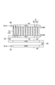
- FIG. 6 is a diagram showing a partial configuration of Example 1 of the line-type solid-state imaging device
- FIG. 7 is a timing chart showing waveforms of respective parts of the line-type solid-state imaging device.
- the imaging region 10 has a plurality of pixel units P arranged in the horizontal direction, and each pixel unit P is a B to the first horizontal register unit 20. Bidirectional charge transfer in the direction and the A direction to the third horizontal register unit 41 is possible.
- the pulse voltage of the clock applied to the electrode P2HB of the multiplication register unit 28 based on the voltage value sequentially supplied from the third horizontal register unit 41 and the amplifier 42 by the signal processing unit 51.
- the value and the DC voltage value applied to the electrode DCB are determined, and a control signal representing this voltage value is output at time t7 (g).
- the driving unit 52 generates an electrode P2HB clock having a pulse voltage corresponding to the determined value, and an electrode DCB DC voltage having a voltage corresponding to the determined value of the signal processing unit 51.
- a clock and a DC voltage are supplied from the drive unit 52 to the multiplication register unit 28 from time t8 to t11 (h), and a clock is input to the second horizontal register unit 24 from time t8 to t9. .
- the charges in the horizontal registers in the second horizontal register unit 24 are sequentially transferred to the multiplication registers in the multiplication register unit 28.
- the charge of each multiplication register in the multiplication register unit 28 is sequentially outputted to the amplifier 30 and outputted from the output port (i). Note that the period from the time t10 to t11 in the clock of the multiplication register unit 28 shown in FIG. 7H is an overclocking period.
- the control unit 50 increases the multiplication register unit 28 according to the amount of the charge.
- the magnification is determined (FIG. 7 (g), time t7). That is, the control unit 50 determines the multiplication factor of the multiplication register unit 28 according to the amount of charge before charge is input to the multiplication register unit 28 (FIG. 7 (h), time t8). (FIG. 7 (g), time t7).
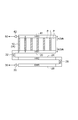
- FIG. 8 is a diagram showing a partial configuration of Example 2 of the line-type solid-state imaging device
- FIG. 9 is a timing chart showing waveforms of each part of the line-type solid-state imaging device.
- the imaging region 10 has a plurality of pixel portions P arranged in the horizontal direction, and each pixel portion P is an output pixel Po divided in the horizontal direction. And a detection pixel Pd.
- the output pixel Po performs charge transfer in the B direction of the first horizontal register unit 20, and the detection pixel Pd performs charge transfer in the A direction of the third horizontal register unit 41.
- each pixel unit P can perform bi-directional charge transfer in the B direction to the first horizontal register unit 20 and in the A direction to the third horizontal register unit 41.
- a clock and a DC voltage are supplied from the driving unit 52 to the multiplication register unit 28 from time t6 to t9 (g), and a clock is input to the second horizontal register unit 24 from time t6 to t7. .
- the charges of the horizontal registers in the second horizontal register unit 24 are sequentially transferred to the multiplication registers in the multiplication register unit 28.
- the charges of the multiplication registers in the multiplication register unit 28 are sequentially output to the amplifier 30 and output from the output port (h). Note that the period from time t8 to t9 in the clock of the multiplication register unit 28 shown in FIG. 9G is an overclocking period.
- the control unit 50 increases the multiplication register unit 28 according to the amount of the charge.
- the magnification is determined (FIG. 9 (f), time t5). That is, the control unit 50 determines the multiplication factor of the multiplication register unit 28 according to the amount of charge before the charge is input to the multiplication register unit 28 (FIG. 9 (g), time t6). (FIG. 9 (f), time t5).
- FIG. 10 is a diagram showing a partial configuration of the interline solid-state imaging device
- FIG. 11 is a timing chart showing waveforms of respective parts of the interline solid-state imaging device.
- the imaging region 10 includes a plurality of pixel portions P and a vertical charge transfer path L that is arranged for each vertical line of the plurality of pixel portions P and performs charge transfer.
- the vertical charge transfer path L is capable of bi-directional charge transfer in the B direction to the first horizontal register unit 20 and in the A direction to the third horizontal register unit 41, and each charge transfer is performed alternately.
- the pulse voltage of the clock applied to the electrode P2HB of the multiplication register unit 28 based on the voltage value sequentially supplied from the third horizontal register unit 41 and the amplifier 42 by the signal processing unit 51.
- the value and the DC voltage value applied to the electrode DCB are determined, and a control signal representing this voltage value is output at time t9 (h).
- the driving unit 52 generates an electrode P2HB clock having a pulse voltage corresponding to the determined value, and an electrode DCB DC voltage having a voltage corresponding to the determined value of the signal processing unit 51.
- a clock and a DC voltage are supplied from the drive unit 52 to the multiplication register unit 28 from time t10 to t14 (i), and a clock is input to the second horizontal register unit 24 from time t10 to t12. .
- the charges of the horizontal registers in the second horizontal register unit 24 are sequentially transferred to the multiplication registers in the multiplication register unit 28.
- the charge of each multiplication register in the multiplication register unit 28 is sequentially output to the amplifier 30 and output from the output port (j). Note that the period from time t13 to t14 in the clock of the multiplication register unit 28 shown in FIG. 11 (i) is an overclocking period.
- the control unit 50 increases the multiplication register unit 28 according to the amount of the charge.
- the magnification is determined (FIG. 11 (h), time t9). That is, the control unit 50 determines the multiplication factor of the multiplication register unit 28 according to the amount of charge before charge is input to the multiplication register unit 28 (FIG. 11 (i), time t10). (FIG. 11 (h), time t9).
- FIG. 12 is a diagram showing a partial configuration of a full-frame transfer type solid-state imaging device
- FIG. 13 is a timing chart showing waveforms of respective parts of the full-frame transfer type solid-state imaging device.
- Each pixel portion P is capable of bi-directional charge transfer in the B direction of the first horizontal register unit 20 and the A direction of the third horizontal register unit 41, and these charge transfers are performed alternately.
- the pulse voltage of the clock applied to the electrode P2HB of the multiplication register unit 28 based on the voltage value sequentially supplied from the third horizontal register unit 41 and the amplifier 42 by the signal processing unit 51.
- the value and the DC voltage value applied to the electrode DCB are determined, and a control signal representing this voltage value is output at time t7 (g).
- the driving unit 52 generates an electrode P2HB clock having a pulse voltage corresponding to the determined value, and an electrode DCB DC voltage having a voltage corresponding to the determined value of the signal processing unit 51.
- a clock and a DC voltage are supplied from the drive unit 52 to the multiplication register unit 28 from time t8 to t11 (h), and a clock is input to the second horizontal register unit 24 from time t8 to t9. .
- the charges in the horizontal registers in the second horizontal register unit 24 are sequentially transferred to the multiplication registers in the multiplication register unit 28.
- the charge of each multiplication register in the multiplication register unit 28 is sequentially outputted to the amplifier 30 and outputted from the output port (i). Note that the period from time t10 to t11 in the clock of the multiplication register unit 28 shown in FIG. 13H is an overclocking period.
- the control unit 50 increases the multiplication register unit 28 according to the amount of the charge.
- the magnification is determined (FIG. 13 (g), time t7). That is, the control unit 50 determines the multiplication factor of the multiplication register unit 28 according to the amount of charge before charge is input to the multiplication register unit 28 (FIG. 13 (h), time t8). (FIG. 13 (g), time t7).
- FIG. 14 is a diagram showing a configuration of a solid-state imaging device according to the third embodiment of the present invention.
- a solid-state imaging device 1B shown in FIG. 14 is a multi-port solid-state imaging device.
- a first horizontal register unit (HR1) 20, a first corner register unit (CR1) 22, Second horizontal register unit (HR2) 24, second corner register unit (CR2) 26, multiplication register unit (EMR) 28, amplifier 30, output port 35, detection unit 40, and control unit 50 is different from that of the first embodiment.
- the solid-state imaging device 1B includes a first horizontal register unit 20a, 20b, 20c, and 20d that receives charges from the partial imaging regions 10a, 10b, 10c, and 10d in the imaging region 10, and a first horizontal register unit 20a. , 20b, 20c, and 20d, the first corner register units 22a, 22b, 22c, and 22d that turn back the charge transfer directions, respectively, and the second corner register units 22a, 22b, 22c, and 22d that receive charges from the respective second register units.
- Horizontal register units 24a, 24b, 24c, and 24d second corner register units 26a, 26b, 26c, and 26d that turn back the charge transfer directions from the second horizontal register units 24a, 24b, 24c, and 24d, respectively.
- the charge from the two corner register units 26a, 26b, 26c, and 26d is multiplied.
- Multiplication registers 28a, 28b, 28c, and 28d, and amplifiers 30a that output voltages corresponding to the amounts of charges received from the multiplication registers 28a, 28b, 28c, and 28d to the output ports 35a, 35b, 35c, and 35d, respectively.
- Control units 50a, 50b, 50c, and 50d are provided for controlling the multiplication factors of the multiplication register units 28a, 28b, 28c, and 28d based on the charged amounts.
- the feedforward control of the multiplication factor of the multiplication register unit described above that is, the real-time control of the multiplication factor of the multiplication register unit is performed for each port. Advantages similar to those of the solid-state imaging device 1 of the embodiment can be obtained.
- the multiplication factor is controlled by adjusting the control voltage of the electrodes of the multiplication register unit.
- the multiplication factor may be controlled by controlling the number of multiplication stages of the multiplication register unit. Specifically, the number of multiplication registers having a charge multiplication effect among a plurality of multiplication registers of the multiplication register unit is controlled. Note that, as described above, a control voltage for performing normal transfer may be supplied to a multiplication register that does not have a charge multiplication function among the multiplication registers (dotted line in FIG. 2B). .
- a multi-port solid-state imaging device having four output ports is exemplified.
- the idea of the present invention is to a multi-port solid-state imaging device having two or more output ports. Applicable.
- the second embodiment can also be applied to a multi-port solid-state imaging device having two or more output ports.
- the idea of the present invention can be applied to various types of solid-state imaging devices such as a line type, an interline type, a frame transfer type, and a full frame transfer type. It is.
- Solid-state imaging device 10 Imaging region 10a, 10b, 10c, 10d Partial imaging region 20, 20a, 20b, 20c, 20d First horizontal register unit (output register unit) 22, 22a, 22b, 22c, 22d First corner register unit 24, 24a, 24b, 24c, 24d Second horizontal register unit (delay register unit) 26, 26a, 26b, 26c, 26d Second corner register section 28, 28a, 28b, 28c, 28d Multiplication register section 30, 30a, 30b, 30c, 30d Amplifier 35, 35a, 35b, 35c, 35d Output port 40 , 40a, 40b, 40c, 40d Detection unit 41 Third horizontal register unit 42 Amplifier 50, 50a, 50b, 50c, 50d Control unit 51 Signal processing unit 52 Drive unit
Landscapes
- Engineering & Computer Science (AREA)
- Multimedia (AREA)
- Signal Processing (AREA)
- Solid State Image Pick-Up Elements (AREA)
- Transforming Light Signals Into Electric Signals (AREA)
Abstract
Description
[第1の実施形態]
[第2の実施形態]
(ライン型の固体撮像装置の例1)
(ライン型の固体撮像装置の例2)
(インターライン型の固体撮像装置)
(フルフレームトランスファ型の固体撮像装置)
[第3の実施形態]
10 撮像領域
10a,10b,10c,10d 部分撮像領域
20,20a,20b,20c,20d 第1の水平レジスタ部(出力レジスタ部)
22,22a,22b,22c,22d 第1のコーナレジスタ部
24,24a,24b,24c,24d 第2の水平レジスタ部(遅延レジスタ部)
26,26a,26b,26c,26d 第2のコーナレジスタ部
28,28a,28b,28c,28d 増倍レジスタ部
30,30a,30b,30c,30d アンプ
35,35a,35b,35c,35d 出力ポート
40,40a,40b,40c,40d 検出部
41 第3の水平レジスタ部
42 アンプ
50,50a,50b,50c,50d 制御部
51 信号処理部
52 駆動部
Claims (9)
- 電荷増倍型の固体撮像装置において、
入射光量に応じた電荷を生成する撮像領域と、
前記撮像領域からの電荷を受ける出力レジスタ部と、
前記出力レジスタ部からの電荷を増倍する増倍レジスタ部と、
を備え、
前記撮像領域からの電荷量に応じて、前記増倍レジスタ部の増倍率のフィードフォワード制御を行う、
固体撮像装置。 - 前記増倍レジスタ部に入力される電荷量を検出する検出部と、
前記検出部によって検出された電荷量に応じて、前記増倍レジスタ部の増倍率のフィードフォワード制御を行う制御部と、
を更に備える、請求項1に記載の固体撮像装置。 - 前記撮像領域からの電荷を受ける検出レジスタ部と、
前記検出レジスタ部から出力される電荷量に応じて、前記増倍レジスタ部の増倍率のフィードフォワード制御を行う制御部と、
を更に備える、請求項1に記載の固体撮像装置。 - 前記出力レジスタ部と前記増倍レジスタ部との間に配置され、前記出力レジスタ部から前記増倍レジスタ部への電荷の転送を遅延させる遅延レジスタ部を更に備える、請求項1又は3に記載の固体撮像装置。
- 前記検出部と前記増倍レジスタ部との間に配置され、前記検出部から前記増倍レジスタ部への電荷の転送を遅延させる遅延レジスタ部を更に備える、請求項2に記載の固体撮像装置。
- 前記制御部は、前記検出部によって検出された電荷量の最大値、最小値及び平均値のうちの何れかに応じて、前記増倍レジスタ部の増倍率の制御を行う、請求項2に記載の固体撮像装置。
- 前記制御部は、前記検出レジスタ部から出力される電荷量の最大値、最小値及び平均値のうちの何れかに応じて、前記増倍レジスタ部の増倍率の制御を行う、請求項3に記載の固体撮像装置。
- 前記検出部はフローティング・ゲート・アンプを含む、請求項2に記載の固体撮像装置。
- 電荷増倍型の固体撮像装置において、
入射光量に応じた電荷を生成する撮像領域と、
前記撮像領域からの電荷を受ける複数の出力レジスタ部と、
前記複数の出力レジスタ部からの電荷をそれぞれ増倍する複数の増倍レジスタ部と、
を備え、
前記複数の増倍レジスタ部にそれぞれ入力される電荷量に応じて、前記複数の増倍レジスタ部の増倍率のフィードフォワード制御をそれぞれ行う、
固体撮像装置。
Priority Applications (4)
| Application Number | Priority Date | Filing Date | Title |
|---|---|---|---|
| KR1020117007770A KR101675605B1 (ko) | 2009-01-30 | 2010-01-22 | 고체 촬상 장치 |
| US13/144,741 US9609247B2 (en) | 2009-01-30 | 2010-01-22 | Solid-state imaging device performing feed-forward control of multiplication factor of multiplication register to match dynamic range of the device with the intensity distribution of incident light |
| CN201080006335.4A CN102301696B (zh) | 2009-01-30 | 2010-01-22 | 固体摄像装置 |
| EP10735757.6A EP2385696B1 (en) | 2009-01-30 | 2010-01-22 | Solid-state imaging device |
Applications Claiming Priority (2)
| Application Number | Priority Date | Filing Date | Title |
|---|---|---|---|
| JP2009-020475 | 2009-01-30 | ||
| JP2009020475A JP5237844B2 (ja) | 2009-01-30 | 2009-01-30 | 固体撮像装置 |
Publications (1)
| Publication Number | Publication Date |
|---|---|
| WO2010087288A1 true WO2010087288A1 (ja) | 2010-08-05 |
Family
ID=42395550
Family Applications (1)
| Application Number | Title | Priority Date | Filing Date |
|---|---|---|---|
| PCT/JP2010/050818 Ceased WO2010087288A1 (ja) | 2009-01-30 | 2010-01-22 | 固体撮像装置 |
Country Status (7)
| Country | Link |
|---|---|
| US (1) | US9609247B2 (ja) |
| EP (1) | EP2385696B1 (ja) |
| JP (1) | JP5237844B2 (ja) |
| KR (1) | KR101675605B1 (ja) |
| CN (1) | CN102301696B (ja) |
| TW (1) | TWI558209B (ja) |
| WO (1) | WO2010087288A1 (ja) |
Cited By (4)
| Publication number | Priority date | Publication date | Assignee | Title |
|---|---|---|---|---|
| WO2012082676A1 (en) * | 2010-12-14 | 2012-06-21 | Truesense Imaging, Inc. | Image sensor with charge multiplication |
| CN102547153A (zh) * | 2010-12-20 | 2012-07-04 | 全视科技有限公司 | 具有电荷倍增输出通道及电荷感测输出通道的图像传感器 |
| US8479374B2 (en) | 2010-12-14 | 2013-07-09 | Truesense Imaging, Inc. | Method of producing an image sensor having multiple output channels |
| US8773564B2 (en) | 2010-12-14 | 2014-07-08 | Truesense Imaging, Inc. | Image sensor with charge multiplication |
Families Citing this family (11)
| Publication number | Priority date | Publication date | Assignee | Title |
|---|---|---|---|---|
| JP5438331B2 (ja) * | 2009-01-30 | 2014-03-12 | 浜松ホトニクス株式会社 | 固体撮像装置 |
| US20110154656A1 (en) * | 2009-11-06 | 2011-06-30 | Harrison Joe A | Systems and methods for manufacturing modified impedance coaxial cables |
| US8553126B2 (en) * | 2010-12-14 | 2013-10-08 | Truesense Imaging, Inc. | Image sensor with charge multiplication |
| US8643758B2 (en) * | 2010-12-20 | 2014-02-04 | Omnivision Technologies, Inc. | Method for processing an image captured by an image sensor having a charge multiplication output channel and a charge sensing output channel |
| US8800130B2 (en) | 2011-05-25 | 2014-08-12 | Truesense Imaging, Inc. | Methods for producing image sensors having multi-purpose architecture |
| US8773563B2 (en) | 2011-05-25 | 2014-07-08 | Truesense Imaging, Inc. | Multi-purpose architecture for CCD image sensors |
| GB201516701D0 (en) * | 2015-09-21 | 2015-11-04 | Innovation & Business Dev Solutions Ltd | Time of flight distance sensor |
| US9930276B2 (en) * | 2016-01-14 | 2018-03-27 | Semiconductor Components Industries, Llc | Methods for clocking an image sensor |
| GB201704452D0 (en) | 2017-03-21 | 2017-05-03 | Photonic Vision Ltd | Time of flight sensor |
| US10805567B2 (en) * | 2018-09-13 | 2020-10-13 | Semiconductor Components Industries, Llc | Imaging pixels with non-destructive readout capabilities |
| CN110335881B (zh) * | 2019-04-30 | 2021-11-16 | 中国电子科技集团公司第四十四研究所 | 电子倍增电荷耦合器件倍增寄存器防杂散信号干扰结构 |
Citations (6)
| Publication number | Priority date | Publication date | Assignee | Title |
|---|---|---|---|---|
| JP2003009000A (ja) * | 2001-06-21 | 2003-01-10 | Fuji Photo Film Co Ltd | 撮像装置 |
| JP2003158679A (ja) * | 2001-08-20 | 2003-05-30 | Fuji Photo Film Co Ltd | 電荷増倍型固体電子撮像装置およびその制御方法 |
| JP3862850B2 (ja) | 1997-03-22 | 2006-12-27 | イー2ヴイ テクノロジーズ (ユーケイ) リミテッド | Ccdイメージャ |
| JP2007124675A (ja) | 2005-10-24 | 2007-05-17 | E2V Technologies (Uk) Ltd | 利得計測構造体 |
| JP2008177709A (ja) * | 2007-01-17 | 2008-07-31 | Hitachi Kokusai Electric Inc | 撮像装置およびその雑音低減方法 |
| JP2008236176A (ja) * | 2007-03-19 | 2008-10-02 | Nec Corp | 電子増倍型撮像装置、電子増倍型撮像装置の校正プログラムおよび校正方法 |
Family Cites Families (13)
| Publication number | Priority date | Publication date | Assignee | Title |
|---|---|---|---|---|
| US6278142B1 (en) | 1999-08-30 | 2001-08-21 | Isetex, Inc | Semiconductor image intensifier |
| US7420605B2 (en) * | 2001-01-18 | 2008-09-02 | E2V Technologies (Uk) Limited | Solid state imager arrangements |
| US7190400B2 (en) * | 2001-06-04 | 2007-03-13 | Texas Instruments Incorporated | Charge multiplier with logarithmic dynamic range compression implemented in charge domain |
| JP3689866B2 (ja) | 2002-05-30 | 2005-08-31 | 日本テキサス・インスツルメンツ株式会社 | Cmd及びcmd搭載ccd装置 |
| US7078670B2 (en) * | 2003-09-15 | 2006-07-18 | Imagerlabs, Inc. | Low noise charge gain circuit and CCD using same |
| JP2005159784A (ja) | 2003-11-27 | 2005-06-16 | Sony Corp | 固体撮像素子及びその駆動方法並びにカメラシステム |
| US20050248676A1 (en) * | 2004-05-08 | 2005-11-10 | Mark Christenson | High-speed frame transfer of sub-frame area |
| JP4442608B2 (ja) * | 2004-07-20 | 2010-03-31 | 株式会社島津製作所 | 固体撮像装置、撮像装置並びに撮像素子 |
| US7485840B2 (en) * | 2007-02-08 | 2009-02-03 | Dalsa Corporation | Semiconductor charge multiplication amplifier device and semiconductor image sensor provided with such an amplifier device |
| JP2008271049A (ja) * | 2007-04-18 | 2008-11-06 | Hamamatsu Photonics Kk | 撮像装置及びそのゲイン調整方法 |
| JP4851388B2 (ja) * | 2007-05-16 | 2012-01-11 | 浜松ホトニクス株式会社 | 撮像装置 |
| JP5438331B2 (ja) | 2009-01-30 | 2014-03-12 | 浜松ホトニクス株式会社 | 固体撮像装置 |
| US8395689B2 (en) * | 2010-12-20 | 2013-03-12 | Omnivision Technologies, Inc. | Image sensor with charge multiplication output channel and charge sensing output channel |
-
2009
- 2009-01-30 JP JP2009020475A patent/JP5237844B2/ja active Active
-
2010
- 2010-01-22 US US13/144,741 patent/US9609247B2/en active Active
- 2010-01-22 EP EP10735757.6A patent/EP2385696B1/en active Active
- 2010-01-22 CN CN201080006335.4A patent/CN102301696B/zh active Active
- 2010-01-22 KR KR1020117007770A patent/KR101675605B1/ko active Active
- 2010-01-22 WO PCT/JP2010/050818 patent/WO2010087288A1/ja not_active Ceased
- 2010-01-27 TW TW099102305A patent/TWI558209B/zh active
Patent Citations (6)
| Publication number | Priority date | Publication date | Assignee | Title |
|---|---|---|---|---|
| JP3862850B2 (ja) | 1997-03-22 | 2006-12-27 | イー2ヴイ テクノロジーズ (ユーケイ) リミテッド | Ccdイメージャ |
| JP2003009000A (ja) * | 2001-06-21 | 2003-01-10 | Fuji Photo Film Co Ltd | 撮像装置 |
| JP2003158679A (ja) * | 2001-08-20 | 2003-05-30 | Fuji Photo Film Co Ltd | 電荷増倍型固体電子撮像装置およびその制御方法 |
| JP2007124675A (ja) | 2005-10-24 | 2007-05-17 | E2V Technologies (Uk) Ltd | 利得計測構造体 |
| JP2008177709A (ja) * | 2007-01-17 | 2008-07-31 | Hitachi Kokusai Electric Inc | 撮像装置およびその雑音低減方法 |
| JP2008236176A (ja) * | 2007-03-19 | 2008-10-02 | Nec Corp | 電子増倍型撮像装置、電子増倍型撮像装置の校正プログラムおよび校正方法 |
Non-Patent Citations (1)
| Title |
|---|
| See also references of EP2385696A4 |
Cited By (6)
| Publication number | Priority date | Publication date | Assignee | Title |
|---|---|---|---|---|
| WO2012082676A1 (en) * | 2010-12-14 | 2012-06-21 | Truesense Imaging, Inc. | Image sensor with charge multiplication |
| US8479374B2 (en) | 2010-12-14 | 2013-07-09 | Truesense Imaging, Inc. | Method of producing an image sensor having multiple output channels |
| EP2672701A1 (en) * | 2010-12-14 | 2013-12-11 | Truesense Imaging, Inc. | Image sensor with charge multiplication |
| US8773564B2 (en) | 2010-12-14 | 2014-07-08 | Truesense Imaging, Inc. | Image sensor with charge multiplication |
| US9136305B2 (en) | 2010-12-14 | 2015-09-15 | Semiconductor Components Industries, Llc | Method of producing an image sensor having multiple output channels |
| CN102547153A (zh) * | 2010-12-20 | 2012-07-04 | 全视科技有限公司 | 具有电荷倍增输出通道及电荷感测输出通道的图像传感器 |
Also Published As
| Publication number | Publication date |
|---|---|
| TW201038068A (en) | 2010-10-16 |
| JP2010178196A (ja) | 2010-08-12 |
| EP2385696A4 (en) | 2015-07-01 |
| JP5237844B2 (ja) | 2013-07-17 |
| CN102301696A (zh) | 2011-12-28 |
| US20110273603A1 (en) | 2011-11-10 |
| US9609247B2 (en) | 2017-03-28 |
| CN102301696B (zh) | 2015-12-02 |
| KR20110107319A (ko) | 2011-09-30 |
| EP2385696A1 (en) | 2011-11-09 |
| EP2385696B1 (en) | 2018-11-28 |
| TWI558209B (zh) | 2016-11-11 |
| KR101675605B1 (ko) | 2016-11-11 |
Similar Documents
| Publication | Publication Date | Title |
|---|---|---|
| JP5237844B2 (ja) | 固体撮像装置 | |
| CN102244741B (zh) | 固态图像传感器和照相机 | |
| US8400546B2 (en) | Image capturing device, image capturing system, and method of driving image capturing device | |
| CN104272718B (zh) | 固体摄像装置 | |
| US20130021509A1 (en) | Solid-state imaging device driving method | |
| CN102164252B (zh) | 固态图像拾取设备及其驱动方法 | |
| JP2009296465A (ja) | 固体撮像装置、その駆動方法及び撮像システム | |
| JP7165873B2 (ja) | 撮像処理回路、撮像システム、撮像処理方法及びプログラム | |
| CN106449668A (zh) | 光电转换元件、装置、距离检测传感器和信息处理系统 | |
| EP2247099B1 (en) | Solid-state imaging device | |
| WO2006009164A1 (ja) | 固体撮像装置、撮像装置並びに撮像素子 | |
| US8754355B2 (en) | Charge multiplying solid state imaging device having multiplication register units with different number of multiplication stages | |
| CN104159050B (zh) | 固态图像传感器、驱动固态图像传感器的方法及电子设备 | |
| CN102246508B (zh) | 固体摄像装置 | |
| JP2008160344A (ja) | 固体撮像装置、カメラシステム、および固体撮像装置の駆動方法 | |
| JP4566013B2 (ja) | 撮像装置 | |
| JP2010081335A (ja) | 撮像装置 | |
| JP4642552B2 (ja) | 撮像装置 | |
| Atlas et al. | Subelectron readout noise focal plane arrays for space imaging | |
| JP2008289072A (ja) | 固体撮像素子の駆動方法及び撮像装置 | |
| JP2013026989A (ja) | 固体撮像素子およびその駆動方法ならびにカメラシステム |
Legal Events
| Date | Code | Title | Description |
|---|---|---|---|
| WWE | Wipo information: entry into national phase |
Ref document number: 201080006335.4 Country of ref document: CN |
|
| 121 | Ep: the epo has been informed by wipo that ep was designated in this application |
Ref document number: 10735757 Country of ref document: EP Kind code of ref document: A1 |
|
| ENP | Entry into the national phase |
Ref document number: 20117007770 Country of ref document: KR Kind code of ref document: A |
|
| WWE | Wipo information: entry into national phase |
Ref document number: 2010735757 Country of ref document: EP |
|
| WWE | Wipo information: entry into national phase |
Ref document number: 13144741 Country of ref document: US |
|
| NENP | Non-entry into the national phase |
Ref country code: DE |